Embed Size (px)
Citation preview

MAHARASHTRA STATE BOARD OF TECHNICAL EDUCATION
(Autonomous)
(ISO/IEC - 27001 - 2005 Certified)
WINTER – 2015 EXAMINATION
Subject Code: 17627 Model Answer Page No:1/29
Important Instructions to examiners: 1) The answers should be examined by key words and not as word-to-word as given in the model
answer scheme.
2) The model answer and the answer written by candidate may vary but the examiner may try to
assess the understanding level of the candidate.
3) The language errors such as grammatical, spelling errors should not be given more Importance
(Not applicable for subject English and Communication Skills.
4) While assessing figures, examiner may give credit for principal components indicated in the
figure. The figures drawn by candidate and model answer may vary. The examiner may give
credit for any equivalent figure drawn.
5) Credits may be given step wise for numerical problems. In some cases, the assumed constant
values may vary and there may be some difference in the candidate’s answers and model answer.
6) In case of some questions credit may be given by judgement on part of examiner of relevant
answer based on candidate’s understanding.
7) For programming language papers, credit may be given to any other
program based on equivalent concept.
Q.1) a) Attempt any THREE of the following: 12
i) With neat diagram describe how physical address is generated in protected mode in
80386 microprocessor.
(Diagram – 2 Marks, Explanation – 2 marks)
Ans.
MAHARASHTRA STATE BOARD OF TECHNICAL EDUCATION
(Autonomous)
(ISO/IEC - 27001 - 2005 Certified)
WINTER – 2015 EXAMINATION
Subject Code: 17627 Model Answer Page No:2/29
Address calculation in protected mode:
The contents of segment registers are used as selectors to address descriptors which contain
the segment limit, base address and access right byte of segment. The effective address
(offset) is added with the segment base address to calculate linear address. This linear
address is used as physical address if the paging unit is disabled.
ii) List any four salient features of pentium processor.
(Any 4 features: 1 mark each)
Ans. Following are the features of Pentium:
1) It is based on net burst micro architecture.
2) Superscalar architecture
3) Dynamic branch prediction
4) Pipelined Floating-Point Unit
5) Separate code and data caches
6) 64-bit data bus
7) Address parity
8) Support for Intel MMX technology
9) Dual power supplies—separate VCC2 (core) and VCC3 (I/O) voltage inputs
10) Separate 16-Kbyte, 4-way set-associative code and data caches, each with improved fully
associative TLBs
11) Pool of four write buffers used by both execution pipelines
12) Enhanced branch prediction algorithm
13) New Fetch pipeline stage between Prefetch and Instruction Decode
iii) List and describe any four features of RISC processor.
(Any 4 features: 1 mark each)
Ans.
1.Simple instruction set: in a RISC machine the instruction set is simple, basic instructions
from which more complex instructions can be composed. Thus instructions with less
latency preferred.
2.Same length Instruction: each instruction is same length so that it may be fetched in
single operation.
3.Single machine cycle instructions: most instruction complete in one machine cycle so
processor handle several instruction at same time. RISC processors have unity CPI (Clock
per Instruction), which is due to the optimization of each instruction on the CPU and
massive pipelining embedded in a RISC processor.
4.Pipelining: Usually massive pipeline is embedded in RISC processor. The pipelining is
key to speed up RISC machine.

MAHARASHTRA STATE BOARD OF TECHNICAL EDUCATION
(Autonomous)
(ISO/IEC - 27001 - 2005 Certified)
WINTER – 2015 EXAMINATION
Subject Code: 17627 Model Answer Page No:3/29
5.Very few addressing modes and formats: the addressing modes are less and having few
formats.
6.Large no of registers: large number of register to prevent large amount of interaction with
memory.
7.Micro coding not required: the instruction micro coding is not required. This is because
of the availability of a set of simple instructions, which can be easily built into hardware.
8.Load and store architecture: the RISC architecture is primarily load and store
architecture, implying that all the memory accesses take place using Load and Store type
operations.
iv) Differentiate between .COM and .EXE programs. (any four points)
(Any four points - 1 marks each)
Ans.
Sr.
No
.COM programs .EXE Programs
1. .COM file does not contain any header .EXE file contains header
2. .COM file cannot contain relocation
items.
.EXE file may contain relocation items.
3. Maximum size is 64k minus 256 bytes.
For PSP and 2 bytes for stack.
No limit on size; Can be of any size
4. Entry point is PSP:0100 Entry point is defined by END
directive.
5. Stack size is 64K minus 256 bytes for
PSP and size of executable data and
code.
Stack size is defined in a program with
STACK directive.
6. Size of file is exact size of program. Size of file is size of program plus
header (Multiple of 256 bytes)
Q.1) b) Attempt any ONE of the following: 6
i) Describe the fields in Control registers of 80386 microprocessor with the help of
neat diagram. (Diagram: 2 Marks, Explanation of CR0 – 2 Marks, Explanation of CR2 and CR3 – 1
Mark each)
Ans. Control Registers: The 80386 has three 32 bit control registers CR0, CR2 and CR3 to
hold global machine status independent of the executed task.
CR0 contains system control flags, which control or indicate conditions that apply to the
system as a whole, not to an individual task.
EM (Emulation, bit 2): EM indicates whether coprocessor functions are to be emulated.
ET (Extension Type, bit 4): ET indicates the type of coprocessor present in the system.

MAHARASHTRA STATE BOARD OF TECHNICAL EDUCATION
(Autonomous)
(ISO/IEC - 27001 - 2005 Certified)
WINTER – 2015 EXAMINATION
Subject Code: 17627 Model Answer Page No:4/29
MP (Math Present, bit 1): MP controls the function of the WAIT instruction, which is used
to coordinate a coprocessor.
PE (Protection Enable, bit 0): Setting PE causes the processor to begin executing in
protected mode. Resetting PE returns to real-address mode.
PG (Paging, bit 31): PG indicates whether the processor uses page tables to translate linear
addresses into physical addresses.
TS (Task Switched, bit 3): The processor sets TS with every task switch and tests TS when
interpreting coprocessor instructions.
CR2 is used for handling page faults when PG is set. The processor stores in CR2 the
linear address that triggers the fault.
CR3 is used when PG is set. CR3 enables the processor to locate the page table directory
for the current task.
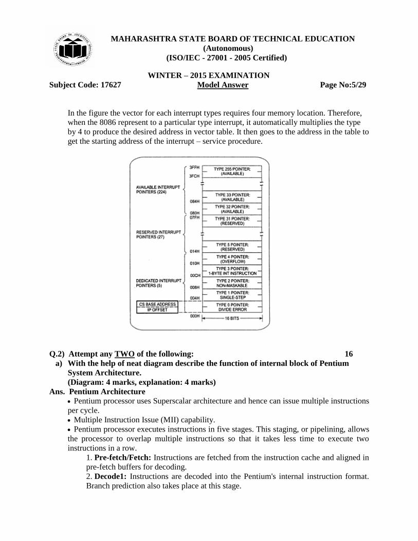
ii) With the help of neat diagram, describe the interrupt vector table entries.
(3 Marks for description and 3 Marks for diagram)
Ans.
Figure shows the 256 interrupt vectors are arranged in the table in memory. Note that the
instruction pointer value is put in as the low word of the vector, and the code segment
register is put in as the high word of the vector. Each double word interrupt vector is
identified by number from 0 to 255. Intel calls this number the type of interrupt.
The lowest five types are dedicated to specific interrupts, such as the divide – by – zero
interrupt, the single step interrupt, and the non maskable interrupt.
Interrupts types 5 to 31 are reserved by intel for using more complex microprocessor, such
as the 80286, 80386, and 80486.
The upper 224 interrupts types, from 32 to 255, are available for use of hardware and
software interrupts,
MAHARASHTRA STATE BOARD OF TECHNICAL EDUCATION
(Autonomous)
(ISO/IEC - 27001 - 2005 Certified)
WINTER – 2015 EXAMINATION
Subject Code: 17627 Model Answer Page No:5/29
In the figure the vector for each interrupt types requires four memory location. Therefore,
when the 8086 represent to a particular type interrupt, it automatically multiplies the type
by 4 to produce the desired address in vector table. It then goes to the address in the table to
get the starting address of the interrupt – service procedure.
Q.2) Attempt any TWO of the following: 16
a) With the help of neat diagram describe the function of internal block of Pentium
System Architecture.
(Diagram: 4 marks, explanation: 4 marks)
Ans. Pentium Architecture
Pentium processor uses Superscalar architecture and hence can issue multiple instructions
per cycle.
Multiple Instruction Issue (MII) capability.
Pentium processor executes instructions in five stages. This staging, or pipelining, allows
the processor to overlap multiple instructions so that it takes less time to execute two
instructions in a row.
1. Pre-fetch/Fetch: Instructions are fetched from the instruction cache and aligned in
pre-fetch buffers for decoding.
2. Decode1: Instructions are decoded into the Pentium's internal instruction format.
Branch prediction also takes place at this stage.

MAHARASHTRA STATE BOARD OF TECHNICAL EDUCATION
(Autonomous)
(ISO/IEC - 27001 - 2005 Certified)
WINTER – 2015 EXAMINATION
Subject Code: 17627 Model Answer Page No:6/29
3. Decode2: Same as above, and microcode ROM kicks in here, if necessary. Also,
address computations take place at this stage.
4. Execute: The integer hardware executes the instruction.
5. Write-back: The results of the computation are written back to the register file.
Branch Prediction Unit: The Pentium processor fetches the branch target instruction
before it executes the branch instruction. The branch prediction algorithm speeds up the
instruction execution. When a branching occurs, a branch instruction address and target
address is saved in Branch target Buffer (BTB). And these BTB records are used after
decoding the branching instruction. And CPU predicts whether the branch will be taken
or not. If the prediction is correct, the process continues and if prediction is incorrect, the
CPU flushes the pipeline and fetches from the correct target address.
The Pentium processor has two separate 8-kilobyte (KB) caches on chip, one for
instruction and one for data. It allows the Pentium processor to fetch data and instructions
from the cache simultaneously. When data is modified, only the data in the cache is
changed. Memory data is changed only when the Pentium processor replaces the
modified data in the cache with a different set of data.
The Pentium processor has been optimized to run critical instructions in fewer clock
cycles than the 80486 processor.
Floating Point Unit: There are 8 general-purpose 80-bit Floating point registers.
Floating point unit has 8 stages of pipelining. First five are similar to integer unit. Since
the possibility of error is more in Floating Point unit (FPU) than in integer unit, additional
error checking stage is there in FPU.
OR

MAHARASHTRA STATE BOARD OF TECHNICAL EDUCATION
(Autonomous)
(ISO/IEC - 27001 - 2005 Certified)
WINTER – 2015 EXAMINATION
Subject Code: 17627 Model Answer Page No:7/29
b) List any four file handling functions of INT 21H. Describe the functions with their
syntax and usages.
(Any four functions – Name and function (usage) - 1 Marks each, their respective
syntax – 1 Mark for each function)
Ans.
1) 3CH : to create file
This function creates a file with indicated attributes and opens the file

MAHARASHTRA STATE BOARD OF TECHNICAL EDUCATION
(Autonomous)
(ISO/IEC - 27001 - 2005 Certified)
WINTER – 2015 EXAMINATION
Subject Code: 17627 Model Answer Page No:8/29
Registers to be used before calling the function using INT 21H:
CX=File Attribute
DS: DX - full file path (zero terminated) – an ASCIIZ String file descriptor;
a start variable in data segment loaded to DX
Syntax: mov ah,3Ch; function 3Ch - create a file
int 21h ; transfer to DOS
2) 3DH: to open file
This function opens the indicated file
Registers to be used before calling the function using INT 21H:
DS: DX - an ASCIIZ String file descriptor
AL=Access Code and sharing modes are as follows
00H- Open for reading mode
01H- open for writing mode
02H – open for read/write mode
Syntax: mov ah,3Dh; function 3Dh - open the file
int 21h; transfer to DOS
3) 3EH: to close the file
This function closes the indicated file
Registers to be used before calling the function using INT 21H :
BX = file handle
Syntax: mov ah, 3Eh; function 3Eh - close a file
int 21h; transfer to DOS
4) 3FH: to read the file
This function reads up to CX bytes from the Indicated file into the specified memory
buffer. On successful return, the AX Register contains the number of bytes actually
read.
Registers to be used before calling the function using INT 21H:
BX = file handle
CX = number of bytes to read
DS:DX -> buffer for data
Syntax: mov ah,3Fh; function 3Fh – read the file
int 21h; transfer to DOS

MAHARASHTRA STATE BOARD OF TECHNICAL EDUCATION
(Autonomous)
(ISO/IEC - 27001 - 2005 Certified)
WINTER – 2015 EXAMINATION
Subject Code: 17627 Model Answer Page No:9/29
5) 40H: to write to the file
This function writes the specified number of bytes from a buffer to a file or device.
Registers to be used before calling the function using INT 21H:
BX = file handle
CX = number of bytes to write
DS:DX -> data to write
Syntax: mov ah,40h; function 40h - write to file
int 21h; transfer to DOS
6) 41H: to delete the file
This function deletes the specified file
Registers to be used before calling the function using INT 21H:
ASCIIZ filename DS: DX - zero terminated full paths.
Syntax: mov ah, 41h; delete file
int 21h; transfer to DOS
7) 56H: to rename the file
This functions renames the given file with new name specified by ES: DI
Registers to be used before calling the function using INT 21H :
DS: DX address of ASCIIZ filename of existing file
ES : DI - ASCIZ new filename
Syntax: mov ah, 56h; delete file
int 21h; transfer to DOS
8) 43H: Set/Get file attribute
This function gets or sets the file attributes
Registers to be used before calling the function using INT 21H:
AL = 00H to get attributes
01H to set attributes
CX = file attributes, if AL=01H. Bits can be combined
DS: DX = segment: offset of ASCIIZ pathname

MAHARASHTRA STATE BOARD OF TECHNICAL EDUCATION
(Autonomous)
(ISO/IEC - 27001 - 2005 Certified)
WINTER – 2015 EXAMINATION
Subject Code: 17627 Model Answer Page No:10/29
Syntax: mov ah, 43h; set/get file attributes
int 21h; transfer to DOS
9) 57H: Set/Get file time & date
This function gets or sets the file date and time.
Registers to be used before calling the function using INT 21H:
AL = 00h 0r 01H (0 - get 1 - set)
BX = file handle
DS: DX = segment: offset of ASCIIZ pathname
Syntax: mov ah, 57h; set/get file date and time
int 21h; transfer to DOS
c) Draw the format of flag register of Intel 80386 microprocessor and describe any four
salient flags of 80386 microprocessor.
(Format – 4 Marks, Any four flag description – 1 mark each) Ans.
Status flags: these reflect the result of the operations performed by the ALU.
CF (D0): Carry Flag – this flag is set when there is a carry out of MSB in case of addition
or borrow in case of subtraction. Few other instructions also affect the carry flag.
PF (D2): Parity Flag – this flag is set when lower byte of the result contains even no. of 1’s
or all zeros.
AF (D4): Auxiliary Carry Flag – this flag is set if there is a carry from lowest nibble i.e. bit
three during addition or borrow from the lowest nibble i.e. bit three during subtraction.
(Remember we always start with the bit0. So the lower byte will be bit7-bit0 and lower
nibble will be bit3-bit0).

MAHARASHTRA STATE BOARD OF TECHNICAL EDUCATION
(Autonomous)
(ISO/IEC - 27001 - 2005 Certified)
WINTER – 2015 EXAMINATION
Subject Code: 17627 Model Answer Page No:11/29
ZF (D6): Zero Flag – this flag is set when the result of any computation is zero.
SF (D7): Sign Flag – this flag is set when the result of any computation is negative. For
signed computations, the sign flag equals the MSB of the result.
OF (D11): Overflow Flag – this flag is set when an overflow occurs i.e. if the result of the
signed operation is large enough to be accommodated in a destination register.
Control flags: there are three control flags and they are used for controlling machine
operation.
TF (D8): Trap Flag – when this flag is set the processor enters single step execution mode.
So a trap interrupt is generated after execution of each instruction. The processor executes
the current instruction and the control is transferred to the Trap interrupt service routine
(ISR).
IF (D9): Interrupt Flag – when this flag is set all the maskable interrupts are recognized.
When this flag is zero then all the maskable interrupts are ignored.
DF (D10): Direction Flag – this is used by string manipulation instructions. When this flag
is zero, the string is processed starting with the lowest address to the highest address i.e.
auto-incrementing mode. Otherwise the string is processed from the highest address towards
the lowest address i.e. auto-decrementing mode.
IOPL (D11&D12): I/O Privilege Level –It specifies one of four different privilege levels
necessary to perform I/O operations. These two bits generally contain 00b when operating in
real mode on the 80386.
NT (D13): Nested Task- controls the operation of an interrupt return (IRET) instruction. NT
is normally zero for real-mode programs.
RF (D16): Resume flag: this flag is used with debug registers breakpoints. It is checked at
the starting of every machine cycle. If it is set, any debug fault is ignored during instruction
cycle. This flag is automatically reset after successful execution of every instruction, except
for IRET and POPF.
VM (D17): Virtual Mode flag- if this flag is set, the 80386 enters the virtual 8086 mode
within the protected mode.
Q.3) Attempt any FOUR of the following: 16
a) Describe the general purpose registers and their functions in pentium processor with
neat diagram.
(Diagram: 2 marks, description 2 marks)
Ans. General purpose registers:
• Four 32-bit registers can be used as
∗ Four 32-bit register (EAX, EBX, ECX, EDX)
∗ Four 16-bit register (AX, BX, CX, DX)
∗ Eight 8-bit register (AH, AL, BH, BL, CH, CL, DH, DL)
• Some registers have special use
∗ ECX for count in loop instructions

MAHARASHTRA STATE BOARD OF TECHNICAL EDUCATION
(Autonomous)
(ISO/IEC - 27001 - 2005 Certified)
WINTER – 2015 EXAMINATION
Subject Code: 17627 Model Answer Page No:12/29
• Two index registers
∗ 16- or 32-bit registers
∗ Used in string instructions
» Source (SI) and destination (DI)
∗ Can be used as general purpose data registers
b) List and describe any four design issues of RISC processor.
(Four design issues: 1mark each)
Ans.
1. Register Window :
2. The reduced hardware requirements of RISC processors leave additional space
available on the chip for the system designer. RISC CPUs generally use this space to
include a large number of registers ( > 100 occasionally).
3. The CPU can access data in registers more quickly than data in memory so having
more registers makes more data available faster. Having more registers also helps reduce
the number of memory references especially when calling and returning from
subroutines.
4. The RISC processor may not be able to access all the registers it has at any given time
provided that it has many of it.

MAHARASHTRA STATE BOARD OF TECHNICAL EDUCATION
(Autonomous)
(ISO/IEC - 27001 - 2005 Certified)
WINTER – 2015 EXAMINATION
Subject Code: 17627 Model Answer Page No:13/29
5. Most RISC CPUs have some global registers which are always accessible. The
remaining registers are windowed so that only a subset of the registers are accessible at
any specific time.
6. To understand how register windows work, we consider the windowing scheme used
by the Sun SPARC processor.
7. The processor can access any of the 32 different registers at a given time. (The
instruction formats for SPARC always use 5 bits to select a source/destination register
which can take any 32 different values.
8. Of these 32 registers, 8 are global registers that are always accessible. The remaining
24 registers are contained in the register window.
9. The register window overlap. The overlap consists of 8 registers in SPARC CPU.
Notice that the organization of the windows are supposed to be circular and not linear;
meaning that the last window overlaps with the first window.
10. Example: the last 8 registers of window 1 are also the first 8 registers of window 2.
Similarly, the last 8 registers of window 2 are also the first 8 registers of window 3. The
middle 8 registers of window 2 are local; they are not shared with any other window.
2. Memory speed issue
Memory speed issues are commonly solved using caches. A cache is a section of fast
memory placed between the processor and slower memory. When the processor wants to
read a location in main memory, that location is also copied into the cache. Subsequent
references to that location can come from the cache, which will return a result much more
quickly than the main memory.
Caches present one major problem to system designers and programmers, and that is the
problem of coherency. When the processor writes a value to memory, the result goes into
the cache instead of going directly to main memory. Therefore, special hardware (usually
implemented as part of the processor) needs to write the information out to main memory
before something else tries to read that location or before re-using that part of the cache
for some different information.
3. Instruction Latency issue
A poorly designed instruction set can cause a pipelined processor to stall frequently.
Some of the more common problem areas are:
Highly encoded instructions---such as those used on CISC machines---that require
complex decoders. Those should be avoided.

MAHARASHTRA STATE BOARD OF TECHNICAL EDUCATION
(Autonomous)
(ISO/IEC - 27001 - 2005 Certified)
WINTER – 2015 EXAMINATION
Subject Code: 17627 Model Answer Page No:14/29
Variable-length instructions which require multiple references to memory to fetch in the
entire instruction. Instructions which access main memory (instead of registers), since
main memory can be slow.
Complex instructions which require multiple clocks for execution (many floating-point
operations, for example.)Instructions which need to read and write the same register. For
example "ADD 5 to register 3" had to read register 3, add 5 to that value, then write 5
back to the same register (which may still be "busy" from the earlier read operation,
causing the processor to stall until the register becomes available.)
Dependence on single-point resources such as a condition code register. If one instruction
sets the conditions in the condition code register and the following instruction tries to
read those bits, the second instruction may have to stall until the first instruction's write
completes.
4. Dependencies issues:
One problem that RISC programmers face is that the processor can be slowed down by a
poor choice of instructions. Since each instruction takes some amount of time to store its
result, and several instructions are being handled at the same time, later instructions may
have to wait for the results of earlier instructions to be stored. However, a simple
rearrangement of the instructions in a program (called Instruction Scheduling) can
remove these performance limitations from RISC programs.
c) State and describe the significance of separate code and data cache in Pentium
processor.
(Significance of separate code and data cache: 4 marks)
Ans. Separate 8K B instruction and Data Cache:
The figure shows the organization of instruction and data cache.

MAHARASHTRA STATE BOARD OF TECHNICAL EDUCATION
(Autonomous)
(ISO/IEC - 27001 - 2005 Certified)
WINTER – 2015 EXAMINATION
Subject Code: 17627 Model Answer Page No:15/29
The Pentium processor has 2 separate 8KB data and code Caches. But they need more
bandwidth than the unified cache.
Both the caches have TLB’s associated with them. The TLBs are used to covert the linear
addresses to the respective physical addresses.
As the data cache stores only 8KB data and code cache stores only instructions, the
lookup process speed for Pentium increases.
Advantages of separate instruction and data caches:
1. Separate code and data cache memories effectively and efficiently executes the branch
prediction.
2. Simultaneous cache look up is achieved by Pentium processor due to the separate data
and code cache.
3. The separate cache memories raise the system performance i.e. an internal read request
is performed more quickly than a bus cycle to memory.
4. They reduce the use of processor’s external bus when the same locations are accessed
multiple times.
d) With the neat diagram, describe the selector fields in 80386 microprocessor.
(Diagram: 2 marks, description; 2marks)
Ans. A protected-mode segment register holds a 16-bit segment selector (see the figure below).
Unlike in real mode, the selector has nothing to do with the segment's location in memory.
Instead, the value in the register is an index into a table of segment descriptors. Each
descriptor defines one segment and determines where the segment resides, the segment
type, and other important parameters such as the access rights.
TI Table indicator:
0 means selector indexes into GDT
1 means selector indexes into LDT

MAHARASHTRA STATE BOARD OF TECHNICAL EDUCATION
(Autonomous)
(ISO/IEC - 27001 - 2005 Certified)
WINTER – 2015 EXAMINATION
Subject Code: 17627 Model Answer Page No:16/29
RPL Privelege level. Linux uses only two privilege levels.
0 means kernel
3 means user
e) Write the stepwise procedure, that an interrupt handler must follow while servicing an
interrupt.
(Steps in sequence: 4 marks)
Ans. Interrupt processing sequence is as given below:
When INT n instruction is executed
1. The processor pushes flag register on stack then the contents of CS And IP register on
stack
2. It clears two flags TF (trap flag) and IE (Interrupt enable flag).
3. Number of interrupt is used to find correct address of ISR in the IVT.
4. Interrupt number (is called as interrupt type) is used to find out the correct address of
ISR in the IVT.
5. The interrupt number is multiplied by 4 to get the address with the IVT that contains the
addresses of ISR.
ISR ADDRESS = Interrupt type x 4
6. All addresses are 4 bytes long. The Interrupt vector address is then filled in CS and IP
register.
7. Finally CPU control is transferred to new address.
8. Same process is followed by for NMI, which automatically generates type 2. No INTA#
cycle is required for NMI.
9. When INTR is made high processor starts first INTA# to indicate acknowledgement and
second is issued to ask for interrupt number to be placed on lower byte of processor data
bus.
10. A special peripheral is designed to respond to the 8086’s interrupt acknowledgment
cycle is the 8259, programmable interrupt controller.

MAHARASHTRA STATE BOARD OF TECHNICAL EDUCATION
(Autonomous)
(ISO/IEC - 27001 - 2005 Certified)
WINTER – 2015 EXAMINATION
Subject Code: 17627 Model Answer Page No:17/29
Q.4) a) Attempt any THREE of the following: 12
i) Describe the DOS-BIOS interface with the help of neat diagram.
(DOS-BIOS interface diagram: 2 marks, description: 2 marks)
Ans. DOS-BIOS interface is as shown in the following diagram:
User programs
DOS
BIOS
Hardware/ Devices
BIOS contains a set of routines in a ROM to provide the device supports. The BIOS tests
and initializes attached devices and provide services that are used for reading to and
writing from the devices.
One task of DOS is to interface with BIOS when there is a need to access its facilities.
When the user program requests a service of DOS, it may transfer the request to BIOS
which in turn accesses the requested device.
Sometimes, a program makes a direct request to BIOS, especially for keyboard and screen
services.
ii) Describe pipelining concept of RISC processor.
(Pipelining concept of RISC processor: 4 marks)
Ans.
A RISC processor pipeline operates in much the same way, although the stages in the
pipeline are different. While different processors have different numbers of steps, they are
basically variations of these five, used in the MIPS R3000 processor:
1. fetch instructions from memory
2. read registers and decode the instruction
3. execute the instruction or calculate an address
4. access an operand in data memory
5. write the result into a register
The length of the pipeline is dependent on the length of the longest step. Because RISC
instructions are simpler than those used in pre-RISC processors (now called CISC, or
Complex Instruction Set Computer), they are more conducive to pipelining. While CISC
instructions varied in length, RISC instructions are all the same length and can be fetched

MAHARASHTRA STATE BOARD OF TECHNICAL EDUCATION
(Autonomous)
(ISO/IEC - 27001 - 2005 Certified)
WINTER – 2015 EXAMINATION
Subject Code: 17627 Model Answer Page No:18/29
in a single operation. Ideally, each of the stages in a RISC processor pipeline should take 1
clock cycle so that the processor finishes an execution of every instruction in same time.
iii) Draw the pipeline stages of floating point unit. Also write the names of stages in
pipelining in Pentium processor.
(Diagram: the pipeline stages of floating point unit: 3 marks, listing of the names of
the pipeline stages of floating point unit: 1mark)
Ans. Diagram of Pipeline stages of floating point unit:
The pipelining stages in the floating point unit of Pentium are:
iv) What is the purpose of MMX architecture designing? Write any four main features
of this technology to fulfill its goals.
(Purpose: 2 marks, four features: 2 marks)
Ans : Purpose of MMX architecture:
Intel’s MMX media enhancement technology is a major extension of the Intel
Architecture that makes PCs into richer multimedia and communications platforms. This
technology introduces 57 instructions oriented to highly parallel operations with
multimedia and communications data types. These instructions use a technique known as

MAHARASHTRA STATE BOARD OF TECHNICAL EDUCATION
(Autonomous)
(ISO/IEC - 27001 - 2005 Certified)
WINTER – 2015 EXAMINATION
Subject Code: 17627 Model Answer Page No:19/29
SIMD (Single Instruction, Multiple Data) to deliver better performance for multimedia
and communications computation. Intel processors that provide MMX technology
support are fully compatible with previous generations of the Intel Architecture and the
installed base of software. To further improve performance, the Pentium II processor,
like the Pentium processor with MMX technology, can execute 2 Intel MMX instructions
at a time.
Features:
1. 57 new microprocessor instructions have been added that are designed to handle video,
audio, and graphical data more efficiently. Programs can use MMX instructions
without changing to a new mode or operating-system visible state.
2. New 64-bit integer data type (Quadword). (4 new MMX data types)
3. A new process, Single Instruction Multiple Data (SIMD), makes it possible for one
instruction to perform the same operation on multiple data items.
4. The memory cache on the microprocessor has increased to 32 KB, meaning fewer
accesses to memory that is off the microprocessor.
5. Eight 64 bits wide MMX technology registers have are added to support the
Multimedia.
5. Write Combining: ⇒ The Write Combining technology of the P6 architecture can be
used to achieve very high graphics I/O performance. This feature combines multiple
writes to a region of memory (for example, a video controller’s frame buffer) declared
as WC type into a single-burst write operation. This is well suited for the bus, which is
optimized for burst transfers. The combining also leads to burst writes of cache line
sizes. These writes are further combined by the chipset, leading to high throughput for
graphics I/O. The result is enhanced multimedia performance, more realistic full-
motion video, and realistic, fast graphics performance.
Q.4) b) Attempt any ONE of the following: 6
i) List any three specific processor extension interface signals of 80386. Also describe
the functions of these signals.
(Any 3 specific processor extension interface signals and their description: 2 marks
each)
Ans. The specific processor extension interface signals of 80386 are:
1. PEREQ: processor extension request active high input signal: It is an input signal for
80386 from the processor extension i.e. coprocessor. When the processor extension
requires the data operand transfer it requests the processor by asserting this signal high

MAHARASHTRA STATE BOARD OF TECHNICAL EDUCATION
(Autonomous)
(ISO/IEC - 27001 - 2005 Certified)
WINTER – 2015 EXAMINATION
Subject Code: 17627 Model Answer Page No:20/29
and issuing it to the processor. It indicates the request to the 80386 to perform a data
operand transfer for a processor extension.
2. PEACK#: processor extension acknowledgement: It is an active low output signal
issued by the processor to the processor extension as an acknowledgement for the request
issued by the coprocessor. If the processor makes this signal low and issues it to the
coprocessor it indicates that the processor is ready to serve the data transfer request for
coprocessor.
3. BUSY#: It is an active low input signal for the 80386. It is issued by the coprocessor to
the processor to indicate that the coprocessor is busy with its allotted job. When this signal
is made low by coprocessor it indicates the 80386 that it is currently busy with the
operation allotted by processor.
4. ERROR#: It is an active low input signal for the 80386. It is issued by the coprocessor
to the processor to indicate that the coprocessor has encountered some error while
performing the operation allotted by CPU and hence it is retrying for the similar operation,
and hence the CPU cannot allot a new task to the coprocessor. Both busy# and error#
indicate the status of operation of processor extension to the CPU.
ii) What do you understand by superscalar execution in Pentium processor?
Describe with neat diagram.
(Superscalar execution: 3 marks, diagram: 3 marks)
Ans : Superscalar executions means which has
Three execution units
One execution unit executes floating point instructions
The other two (U pipe and V pipe) execute integer instructions
Parallel execution of several instructions – superscalar processor
Diagram of superscalar execution in Pentium is as given below

MAHARASHTRA STATE BOARD OF TECHNICAL EDUCATION
(Autonomous)
(ISO/IEC - 27001 - 2005 Certified)
WINTER – 2015 EXAMINATION
Subject Code: 17627 Model Answer Page No:21/29
The first stage of the pipe-line is Prefetch (PF) stage in which instructions are
prefetched from the on chip instruction cache or memory . Because the Pentium processor
has separate caches for instructions and data, prefetches no longer conflict with data
references for access to the cache. If the requested line is not in the code cache, a memory
reference is made. In the PF stage, two independent pairs of line-size (32-byte) prefetch
buffers operate in conjunction with the branch target buffer. This allows one prefetch
buffer to prefetch instructions sequentially, while the other prefetches according to the
branch target buffer predictions. The prefetch buffers alternate their prefetch paths.
The next pipe-line stage is Decode1 (D1) in which two parallel decoders attempt to
decode and issue the next two sequential instructions. The decoders determine whether
one or two instructions can be issued contingent upon the instruction pairing rules. The
Pentium processor will decode near conditional jumps (long displacement) in the second
opcode map in a single clock in either pipe-line.
The D1 stage is followed by Decode 2 (D2) in which the address of memory
resident operands is calculated.
The Execute (EX) stage of the pipe line for both ALU operations and for data cache
access; therefore those instructions specifying both an ALU operation and a data cache
access will require more than one clock in this stage. In EX all u-pipe instructions and all
v-pipe instructions except conditional branches are verified for correct branch prediction.
Microcode is designed to utilize both pipe-lines and thus those instructions requiring
microcode execute.
The final stage is Write-back (WB) where instructions are enabled to modify processor
state and complete execution. In this stage v-pipe conditional branches are verified for
correct branch prediction. All the registers and memory locations are updated in this stage.
Q.5) Attempt any TWO of the following: 16
a) Describe any four the floating point exceptions in Pentium
(Any four floating point exceptions -2 marks each)
Ans. The Pentium provides six floating point exceptions
1. Invalid operation (#I)
Stack overflow or underflow (#IS)
Invalid arithmetic operation (#IA)
2. Divide-by-zero (#Z).
3. Demoralized operand (#D)

MAHARASHTRA STATE BOARD OF TECHNICAL EDUCATION
(Autonomous)
(ISO/IEC - 27001 - 2005 Certified)
WINTER – 2015 EXAMINATION
Subject Code: 17627 Model Answer Page No:22/29
4. Numeric overflow (#O)
5. Numeric underflow (#U)
6. Inexact result (precision)(#P).
Each of the six exception classes have a corresponding flag bit in the FPU status word and
a mask bit in the FPU control word.
Denormal
The denormal exception occurs if one or more of the operands is a denormal number. This
exception is never regarded as an error.
Divide-by-Zero Exception
A divide-by-zero exception occurs for a floating-point division operation if the divisor is
zero and the dividend is finite and non-zero. It also occurs for other operations in which
the operands are finite and the correct answer is infinite.
When the divide by zero exception is masked, the result is +/-infinity. The following
specific cases cause a zero-divide exception:
LOG(0.0)
LOG10(0.0)
Overflow Exception
An overflow exception occurs if the rounded result of a floating-point operation contains
an exponent larger than the numeric processing unit can represent. A calculation with an
infinite input number is not sufficient to cause an exception.
When the overflow exception is masked, the calculated result is +/-infinity or the +/-
largest represent able normal number depending on rounding mode. When the exception
is not masked, a result with an accurate significant and a wrapped exponent is available to
an exception handler.
Underflow Exception
The underflow exception occurs if the rounded result has an exponent that is too small to
be represented using the floating-point format of the result.
If the underflow exception is masked, the result is represented by the smallest normal
number, a denormal number, or zero. When the exception is not masked, a result with an
accurate significant and a wrapped exponent is available to an exception handler
Inexact Exception
The inexact exception occurs if the rounded result of an operation is not equal to the
unrounded result.
It is important that the inexact exception remain masked at all times because many of the
numeric library procedures return with an undefined inexact exception flag. If the inexact
exception is masked, no special action is performed. When this exception is not masked,
the rounded result is available to an exception handler.

MAHARASHTRA STATE BOARD OF TECHNICAL EDUCATION
(Autonomous)
(ISO/IEC - 27001 - 2005 Certified)
WINTER – 2015 EXAMINATION
Subject Code: 17627 Model Answer Page No:23/29
b) With the neat diagram, describe the use of debug registers in 80386 microprocessor.
(Diagram 3 marks, explanation 5 marks)
Ans.
OR

MAHARASHTRA STATE BOARD OF TECHNICAL EDUCATION
(Autonomous)
(ISO/IEC - 27001 - 2005 Certified)
WINTER – 2015 EXAMINATION
Subject Code: 17627 Model Answer Page No:24/29
There are eight debug registers DR0 to DR7 for hardware debugging.
The DR0 to DR3 are used to store program controllable breakpoint addresses.
The DR4 and DR5 are not used and are reserved by Intel.
The DR6 and DR7 are used to hold the breakpoint status and breakpoint control
information respectively.
Debug Address Registers (DR0-DR3)
Each of these registers contains the linear address associated with one of four breakpoint
conditions. Each breakpoint condition is further defined by bits in DR7.
Debug Control Register (DR7)
The debug control register shown in figure both helps to define the debug conditions and
selectively enables and disables those conditions.
For each address in registers DR0-DR3, the corresponding fields R/W0 through R/W3
specify the type of action that should cause a breakpoint. The processor interprets these bits
as follows:
00 -- Break on instruction execution only
01 01 -- Break on data writes only
10 -- undefined
11 -- Break on data reads or writes but not instruction fetches
Fields LEN0 through LEN3 specify the length of data item to be monitored. A length of 1,
2, or 4 bytes may be specified. The values of the length fields are interpreted as follows:
00 -- one-byte length
01 -- two-byte length
10 -- undefined
11 -- four-byte length
If R/W n is 00 (instruction execution), then LENn should also be 00. Any other length is
undefined.
The low-order eight bits of DR7 (L0 through L3 and G0 through G3) selectively enable the
four address breakpoint conditions.
The LE and GE bits control the "exact data breakpoint match" feature.
Debug Status Register (DR6)
The debug status register shown in figure permits the debugger to determine which debug
conditions have occurred.
When the processor detects an enabled debug exception, it sets the low-order bits of this
register (B0 thru B3) before entering the debug exception handler.
The BT bit is associated with the T-bit (debug trap bit) of the TSS (refer to 7 for the
location of the T-bit). The processor sets the BT bit before entering the debug handler if a
task switch has occurred and the T-bit of the new TSS is set.

MAHARASHTRA STATE BOARD OF TECHNICAL EDUCATION
(Autonomous)
(ISO/IEC - 27001 - 2005 Certified)
WINTER – 2015 EXAMINATION
Subject Code: 17627 Model Answer Page No:25/29
The BS bit is associated with the TF (trap flag) bit of the EFLAGS register. The BD bit is
set if the next instruction will read or write one of the eight debug registers and ICE-386 is
also using the debug registers at the same time.
Note that the bits of DR6 are never cleared by the processor.
c) List any eight features of SUN Ultra SPARC.
(List any 8 features of SUN ULTRA SPARC -1 mark each)
Ans.
Following are features of SUN ULTRA SPARC :
1.14 stage non stalling pipeline
2. Six execution units including two integers, 2 for floating, 1 for load/store and 1 for
address generation unit.
3 It has a large number of buffers, but only load/store unit, it dispatches them one
instruction at a time from the instruction stream.
4. It contains 32KB L1 instruction cache, 64KB L1 data cache, 2KB prefetch cache and
2KB write cache.
5. It contains instructions to support multimedia.
6. One major limitation of SPARC is its low speed compared to most of modern processor.
7. It stores multibyte numbers using BIG endian format.
8. It supports a pipelined floating point processor. The FPU has five separate functional
units for performing floating point operations.
Q.6) Attempt any FOUR of the following: 16
a) Compare real mode and protected mode of 80386 (any four points).
(Any four points 1 Mark each)
Ans.
Sr. No
Real Mode
Protected Mode
1 It uses 20 address lines It uses 32 bit address lines
2 It access only 1MB memory It access only 4GB memory
3 Segmentation is used Paging is used
4 Protection is not available Protection is available
5 Selector is not required in
address generation
Selector is required in address

MAHARASHTRA STATE BOARD OF TECHNICAL EDUCATION
(Autonomous)
(ISO/IEC - 27001 - 2005 Certified)
WINTER – 2015 EXAMINATION
Subject Code: 17627 Model Answer Page No:26/29
b) What is RISC processor? How does it differ from CISC processor?
(RISC PROCESSOR -1 Mark, difference 3 marks)
Ans. Reduced instruction set computer (RISC):
To execute each instruction if there is separate electronic circuitry in control unit, which
produce all necessary signals, this approach of design of control section of processor is
called Reduced instruction set computer(RISC)
Modern processors almost are all RISC.
Even CISC instruction sets (x86-64) are translated to RISC microcode on chip prior to
execution.
But the general differences are:
CISC - larger, more feature-rich instruction set (more operations, addressing modes,
etc.). slower clock speeds. fewer general purpose registers. Examples: x86 variants
RISC - smaller, simpler instruction set. faster clock speeds. more general purpose
registers. Examples: MIPS, Itanium, PowerPC
Practical implications:
An equivalent program implemented in CISC will most likely be shorter than a program
implemented in RISC (because RISC combines multiple simple instructions to replicate the
complex instructions provided by CISC).
RISC CPUs generally run at faster clock speeds than CISC because max clock period is
dictated by the slowest step of the pipeline (more complex instructions are slower).
c) Write any four practical performance issues in pipeline systems.
(Any 4 issues -1 mark each)
Ans.
Pipelining increases the CPU instruction throughput - the number of instructions completed
per unit of time. But it does not reduce the execution time of an individual instruction. In
fact, it usually slightly increases the execution time of each instruction due to overhead in
the pipeline control.
The increase in instruction throughput means that a program runs faster and has lower total
execution time.

MAHARASHTRA STATE BOARD OF TECHNICAL EDUCATION
(Autonomous)
(ISO/IEC - 27001 - 2005 Certified)
WINTER – 2015 EXAMINATION
Subject Code: 17627 Model Answer Page No:27/29
Limitations on practical depth of a pipeline arise from:
Instruction latency:
A poorly designed set can cause a pipelined processor to stall frequently. Some of the
more typical CISC instruction which have more instruction latency should avoided
Dependency Issues:
Dependence on single point resource such as a condition code register. If one instruction
sets the conditions in the condition code register and the following instruction tries to read
those bits, the second instruction may have to stall until the first instruction's write
completes.
Cautions on the use of RISC:
The transition from CISC to RISC design strategy is, not without its problem. The
software engineers should be aware of the key issues which arises when moving code
from a CISC processor to a RISC:
Code quality, Scheduling, Debugging, Code expansion, On chip cache.
Imbalance among pipeline stages.
Imbalance among the pipe stages reduces performance since the clock can run no faster
than the time needed for the slowest pipeline stage;
d) Write any four features of Pentium II processor.
(Any four features 1 mark each)
Ans. Features of Pentium II:
1. It is a 32-bit processor.
2. It has a full 32-bit data bus.
3. It has an integrated math coprocessor (sometimes called a "floating point unit").
4. It supports MMX instructions, which are useful for video decoding and playback, as
well as 3D gaming.
5. It has it's L2 cache integrated into the processor die itself, rather than on the
motherboard. This makes it slightly faster at the same clock speed, since it does not
take as long to fetch data from the cache.

MAHARASHTRA STATE BOARD OF TECHNICAL EDUCATION
(Autonomous)
(ISO/IEC - 27001 - 2005 Certified)
WINTER – 2015 EXAMINATION
Subject Code: 17627 Model Answer Page No:28/29
6. It has more L2 cache, and is packaged (in desktop processors) in a slot cartridge,
rather than a socket.
e) Describe the structure of MS-DOS with the help of neat diagram. (Diagram 2 marks, explanation 2 marks)
Ans.
BIOS:- A BIOS is specific to individual computer system and it is provided by the manufacturer
of the system. It contains device driver for the following devices.
1) Keyboard
2) Printer
3) Auxilary device
4) Date and time
5) Boot disk device

MAHARASHTRA STATE BOARD OF TECHNICAL EDUCATION
(Autonomous)
(ISO/IEC - 27001 - 2005 Certified)
WINTER – 2015 EXAMINATION
Subject Code: 17627 Model Answer Page No:29/29
DOS - Kernel :- The Kernel is a proprietary program supplied by Microsoft corporation & provides
collection of hardware independent services on system function such as :
File & Record Management
Memory Management
Character Device I/O
Spawning of other program
Access to the real time clock
Command Processor :-
Intrinsic command → internal command
Extrinsic command → external command
It is the user interface to the operating system. It is responsible for carrying out the
commands i.e. loading or execution of program from the disk or mass storage device.
The default shall command is command.com. It is a program under the control of MS –
DOS. It is fetcher divided into:
A resident portion – at low portion of memory.
Initialization section – at middle portion of the memory.
Transient Module – at the high end of the memory.
The user commands are divided into three categories :
1) Internal Commands :- Intrinsic command by command.com eg. copy, rename, delete etc.
2) External commands :- Extrinsic command eg. check disk, back – up etc.
3) Batch file :-
There are the text files containing list of extrinsic & intrinsic commands