Embed Size (px)
Citation preview
P. Harichandana et al Int. Journal of Engineering Research and Applications www.ijera.com
ISSN : 2248-9622, Vol. 3, Issue 5, Sep-Oct 2013, pp.1807-1813
www.ijera.com 1807 | P a g e
Improvement of DVR Performance Using Fast and Effective
Control Scheme under Various Loads
P. Harichandana, M. Tech Scholar*, Madhavi Sunkara, M. Tech** *(Department of Electrical and Electronics Engineering, GEC Gudlavalleru, Andhra Pradesh, India)
** (Department of Electrical and Electronics Engineering, GEC Gudlavalleru, Andhra Pradesh, India)
ABSTRACT The dynamic voltage restorer (DVR) has become popular as a cost effective and efficient solution for the
protection of sensitive loads from voltage sags. This paper reports a novel control scheme for DVR to achieve fast response and effective sag compensation capabilities. The DVR, which is placed in series with sensitive
load, must be able to respond quickly to voltage sag if end user’s of sensitive equipment are to experience no
voltage fluctuations. But the proposed control scheme is controls the magnitude and phase angle of the injected
voltage for each phase separately. Fast least error squares digital filters are used to estimate the magnitude and
phase of the measured voltages. The utilized least error squares estimated filters considerably reduce the effects
of noise, harmonics and disturbances on the estimated phasor parameters. This enables the DVR to detect and
compensate voltage sags accurately, under linear and non linear load conditions. The proposed control system
does not need any phase locked loops. It also effectively limits the magnitude of the modulating signals to
prevent over-modulation. Both sides, separately controlling the injected voltage in phase enable the DVR to
restore load voltage in short time interval (5ms) with zero steady state. Results of the simulation studies in the
MATLAB/SIMULINK software environment indicate that the proposed control scheme performs satisfactorily
under linear, non linear loads and BLDC motor drive.
Keywords – BLDC motor, DVR, Least error square digital filters, voltage sag.
I. INTRODUCTION Electric power quality is capacity of an
electric power system to supply electric energy of a
load in an acceptable quality. Power distribution
system should provide with an uninterrupted flow of
energy at smooth sinusoidal voltage at the contracted
magnitude level and frequency to their customers. Power systems especially distribution systems, have
numerous non linear loads, which significantly affect
the quality of power. Apart from non linear loads like
capacitor switching, motor starting and unusual faults
could also inflict power quality problems. Many
problems can result from poor power quality (PQ),
especially in today’s complex power system, such as
the false operation of modern control systems. Voltage
sag is an important PQ problem because of sensitive
loads growth. Worldwide experience has showed that
short circuit faults are the main origin of voltage sag;
therefore there is a loss of voltage quality [1]-[3]. Voltage sag is defined as a sudden reduction
in supply voltage to between 90% and 10% of the
nominal value, followed by a recovery after a short
interval (the standard duration of sag is between 10
milliseconds and 1 minute). The most common
compensator for voltage sag is the dynamic voltage
restorer (DVR). The basic operation of the DVR is
based on injection of a compensation voltage with
required magnitude, phase angle and frequency in
series with the sensitive electric distribution feeder.
A dynamic voltage restorer (DVR) can eliminate most
sags and minimize the risk of load tripping during sags
[2], [3]-[5]. It injects appropriate three phase ac
voltages in series with the supply, when voltage sag is
detected./Considering the shortcomings of the
preceding methods, a fast and effective control
scheme for the DVR is proposed in this paper. Three
identical control systems are used to control the
injected voltage in each phase independently. Three
single phase H-bridge VSIs are utilized to generate sinusoidal voltages. The proposed multi loop control
system [1], [3], [9], [13] is comprised of an outer
phasor-based load voltage control system and an inner
injected voltage-control system. The phasor
parameters of the measured supply and load voltages
are estimated by using least error squares (LES) filters
[15] in a short time interval (5 ms). LES filters are
widely used for fast and reliable phasor parameter
estimation in digital protection systems. On the other
hand, the inner injected voltage-control system is
utilized for damping the transient resonant oscillations caused by the harmonic filter to improve the dynamic
response and stability of the DVR.
The performance of the proposed control
scheme is evaluated by using MATLAB/SIMULINK
software. The study results indicate that the proposed
control strategy has the following advantages:
It regulates the load voltage negative- and zero-
sequence components as well as the positive-
sequence component in a considerably short time
RESEARCH ARTICLE OPEN ACCESS

P. Harichandana et al Int. Journal of Engineering Research and Applications www.ijera.com
ISSN : 2248-9622, Vol. 3, Issue 5, Sep-Oct 2013, pp.1807-1813
www.ijera.com 1808 | P a g e
period (5 ms), with zero steady state error and
without phase jump.
The proposed DVR system can be used in both
four wired and three wired distribution systems,
or even in a single phase configuration.
The proposed method to limit the magnitude of the modulating signals without distorting the
injected voltage wave-shape.
The utilized LES filters the effects of noise,
harmonics and disturbances on the estimated
parameters. This results in accurate sag detection
and compensation under nonlinear load
conditions.
The proposed control strategy does not need
phase locked loops, because the phase angles of
the measured voltages are estimated by using the
LES filters in 5 ms.
Due to the inherent characteristics of the proposed control scheme, there is no need for utilizing
complicated controllers. Therefore, simple PI and
proportional controllers are utilized in this paper.
II. Dynamic Voltage Restorer Dynamic voltage restorer was originally
proposed to compensate for voltage disturbances on
distribution systems. A typical DVR scheme is shown
in Fig. 1. The restoration is based on injecting AC voltages in series with the incoming three-phase
network, the purpose of which is to improve voltage
quality by adjustment in voltage magnitude, wave-
shape, and phase shift. As shown in Fig. 1, the DVR
essentially consists of a series-connected injection
transformer Ti, a voltage-source inverter (VSI), a
harmonic filter, and an energy storage device [4], [13].
Meanwhile, a parallel switch is used to bypass and
protect the DVR, when a downstream fault is detected
[14], [15]. As shown in Fig. 1, the line-side harmonic
filter topology [11] consists of the leakage inductance of the injection transformer and the filter capacitor.
Meanwhile, denotes the dc-link capacitor.
The series injected voltage of the DVR,
Vdvr, is synthesized by modulating pulse widths of
the inverter-bridge switches. The injection of an
appropriate Vdvr in the face of an up-stream voltage
disturbance requires a certain amount of real and
reactive power supply from the DVR. The reactive
power requirement is generated by the inverter.
Fig. 1: schematic diagram of the DVR with line side
harmonic filter
Widely used in present DVR control is the so-called in
phase voltage injection technique where the load
voltage V2 is assumed to be in-phase with the pre-sag
voltage. As the DVR is required to inject active power
into the distribution line during the period of compensation, the capacity of the energy storage unit
can become a limiting factor in the disturbance
compensation process. In particular, if capacitors are
used as energy storage, the DC-link voltage will
decrease with the dwindling storage energy during
compensation.
Fig. 2: Vector Diagram of Voltage Injection Method
The corresponding phasor diagram
describing the electrical conditions during voltage sag
is depicted, where only the affected phase is shown for
clarity. Let the voltage quantities Il, φ, δ and α
represent the load current, load power factor angle,
supply voltage phase angle and load voltage advance
angle respectively. Although there is a phase
advancement of α in the load voltage with respect to
the pre-sag voltage in Fig. 2, only in-phase
compensation where the injected voltage is in phase with the supply voltage (α = δ) is considered. The
block diagram of the proposed DVR control system
for one phase is depicted in Fig. 2. Assume that the
fundamental frequency components of the supply
(grid-side) and load phase voltages are defined by (1)
and (2), respectively.
𝑣𝑠 = 𝑉𝑠 × 𝑐𝑜𝑠 𝑤𝑡 + 𝜃𝑠 1 𝑣𝑙 = 𝑉𝑙 × 𝑐𝑜𝑠 𝑤𝑡 + 𝜃𝑙 2 As shown in Fig. 2, a multi-loop control system is
used to improve the transient and steady-state
responses of the DVR. The proposed control system is
comprised of an outer phasor based load voltage
control system and an inner injected voltage control
system. The former generates a reference signal for
the latter.
The presag phasor of the supply voltage is denoted by
𝑉 𝑝𝑟𝑒 = 𝑉𝑝𝑟𝑒∠𝜃𝑝𝑟𝑒 . 𝑉𝑝𝑟𝑒 is assumed to be equal to the
nominal phase voltage rms value. Meanwhile, 𝜃𝑝𝑟𝑒 is
determined by using a phase freezer unit.

P. Harichandana et al Int. Journal of Engineering Research and Applications www.ijera.com
ISSN : 2248-9622, Vol. 3, Issue 5, Sep-Oct 2013, pp.1807-1813
www.ijera.com 1809 | P a g e
III. Proposed DVR Control Scheme
Fig. 3: Block diagram of the DVR control scheme for each phase
The function of the phase freezer is to fix
(Freeze) the presag phase angle of the supply voltage,
to be used as the reference phase angle of the load
voltage, as described in [1], [6], and [9]. The sag
detection unit enables the phase freezer unit when 𝑉𝑠 becomes less than 0.95 p.u. of the nominal phase voltage (during voltage sags). It must be noted that
the proposed control scheme does not need a PLL,
because the voltage phase angle is estimated by using
the LES filter.
3.1 Load Voltage control system
The phasor-based load voltage-control
system restores the fundamental frequency
component of the load voltage to its presag
conditions. Based on the presag compensation
method, the voltage phasor, which must be injected by the DVR, is the complex difference between the
supply voltage phasor and the presage supply voltage
phasor, as shown in the vector diagram of Fig. 4. This
phasor (the feed forward-injected voltage phasor
𝑉𝑖𝑛𝑗∗
1= 𝑉𝑖𝑛𝑗 1
∗ ∠𝜃𝑖𝑛𝑗 1∗ ) is calculated by the phasor
subtraction unit, shown in Fig. 4 according to (3) and
(4). The coefficient 𝛾 in (3) is 1 when𝑉𝑝𝑟𝑒 𝑐𝑜𝑠𝜃𝑝𝑟𝑒 >
𝑉𝑠𝑐𝑜𝑠𝜃𝑠; otherwise it is -1
𝑉𝑖𝑛𝑗 1∗ = 𝛾 ×
𝑉𝑝𝑟𝑒 𝑐𝑜𝑠𝜃𝑝𝑟𝑒 −𝑉𝑠𝑐𝑜𝑠𝜃𝑠 2
+
(𝑉𝑝𝑟𝑒 𝑠𝑖𝑛𝜃𝑝𝑟𝑒 −𝑉𝑠𝑠𝑖𝑛𝜃𝑠)2
(3)
𝜃𝑖𝑛𝑗 1∗ = 𝐴𝑟𝑐 𝑡𝑎𝑛
𝑉𝑝𝑟𝑒 𝑠𝑖𝑛𝜃𝑝𝑟𝑒 −𝑉𝑠𝑠𝑖𝑛𝜃 𝑠
𝑉𝑝𝑟𝑒 𝑐𝑜𝑠𝑝𝑟𝑒 −𝑉𝑠𝑐𝑜𝑠𝜃 𝑠
(4)
Two PI controllers (𝐶1 and𝐶2) are used to eliminate the steady state errors of the magnitude and
phase angle of the load voltage, respectively. These
controllers compensate dc error signals. Therefore,
their parameters are set simply by a try-and-error
method in order to achieve a fast response with zero
steady-state error and without an observable
overshoot.
Fig. 4: Vector diagram of the phasor subtraction unit
The outputs of the PI controllers 𝑉𝑖𝑛𝑗 2∗
and𝜃𝑖𝑛𝑗 2∗ are added to the outputs of the feed-forward
loop 𝑉𝑖𝑛𝑗 1∗ and θinj 1
∗ to achieve the overall output
phasor of the outer voltage-control loop as
𝑉𝑖𝑛𝑗∗ = 𝑉𝑖𝑛𝑗
∗ ∠𝜃𝑖𝑛𝑗∗ = (𝑉𝑖𝑛𝑗 1
∗ + 𝑉𝑖𝑛𝑗 2∗ )∠ 𝜃𝑖𝑛𝑗 1
∗ + 𝜃𝑖𝑛𝑗 2∗
(5)
3.2 Injected Voltage Control System
Voltage sags could be effectively
compensated if the output of the phasor-based control
system Vinj∗ was fed to the sinusoidal pulse width
modulation (SPWM) unit. However, the harmonic
filter resonances could not be eliminated under these
conditions. Therefore, in order to improve the
stability and dynamic response of the DVR, an
injected voltage controller and a filter capacitor
current controller are utilized, which attenuate the
harmonic filter resonances.
The generated reference signal for the
injected voltage Vinj∗ is compared with the measured
injected voltageVinj , and the error is fed to the voltage
controller. The utilized voltage controllerC3 is a 𝑃
controller with the proportional gain of kv. As shown
in Fig. 3, the output of the voltage controller icap∗ is
the reference signal for the filter capacitor current
control loop. It is compared with the measured
capacitor current and the error is fed to the current
controller Cp , which is a P controller with the gain
kc .

P. Harichandana et al Int. Journal of Engineering Research and Applications www.ijera.com
ISSN : 2248-9622, Vol. 3, Issue 5, Sep-Oct 2013, pp.1807-1813
www.ijera.com 1810 | P a g e
A large kv means high amplification of the
DVR filter resonance, which will affect the system
stability. Thus, the desirable transient response (fast
response) of the DVR is provided by using a feed-
forward loop, and low proportional gain is utilized as
the voltage controller. On the other hand, a large kc
will damp the harmonic filter resonance more
effectively, but kc is always limited due to practical
considerations, such as amplifications of capacitor
current noise, measurement noise, and dc offset [12].
Therefore, the lowest value of the proportional gain,
which still damps the resonances effectively, is
utilized as the current controller. The output of the
current controller is added to the feed-forward
voltage to derive the control (modulating) signal for the PWM generator of the inverter.
IV. Modeling and Simulation Results 4.1 Sag Compensation under Linear Loads
The performance of the proposed DVR
control scheme during voltage sags caused by single
line-to-ground (SLG) and line-to-line (LL) faults
under linear load conditions is investigated in this
subsection. The DVR is protected by using a 10-kVA
linear load with a power factor of 0.9.
4.1.1 Single Line-to-Ground Fault
Fig.5: Simulation model of sag compensation during
SLG fault under Linear Load
Modeling circuit and results of simulations
for SLG fault with a fault resistance of 0.5Ω are
shown in Figs. 5 and 6. The short-circuit, taking
place on 30% of the length of the parallel
transmission line connected to starts at 0.08sec and is
cleared at 0.16sec. Fig. 7(a)–(c) depicts the injected
voltages for the depressed phases, the restored load
voltages, and DC-Link voltage.
Fig.6: (a) Supply Voltage. (b) Estimated RMS supply
Voltage of depressed phase. (c) Injected Voltage
magnitudes for the depressed voltage.
Fig.7: (a) Load Voltage. (b) Injected Voltages for the
depressed Phase. (c) DC-Link Voltage.
4.1.2 Line-to-Line Fault
Fig.8: (a) Supply Voltage. (b) Estimated RMS supply
Voltage of depressed phases. (c) Injected Voltage
magnitudes for the depressed voltage.
The results of simulations for voltage sag
caused by a Line-to-Line fault with a resistance of
0.5 are depicted in Fig. 8. The fault, taking place on
50% of the transmission-line length, starts at 0.08sec
and is cleared at 0.18sec.

P. Harichandana et al Int. Journal of Engineering Research and Applications www.ijera.com
ISSN : 2248-9622, Vol. 3, Issue 5, Sep-Oct 2013, pp.1807-1813
www.ijera.com 1811 | P a g e
Fig.9: (a) Load Voltage. (b) Injected Voltages for the
depressed Phases. (c) DC-Link Voltage.
As shown in Fig. 9(a)–(c) depicts the
injected voltages for the depressed phases, the
restored load voltages, and DC-Link voltage.
4.2 Sag Compensation under Non-Linear Loads
4.2.1 Single Line-to-Ground Fault
The performance of the proposed DVR
control scheme during voltage sags caused by single
line-to-ground (SLG) and line-to-line (LL) faults under non linear load conditions is investigated in
this subsection.
Fig.10: Simulation Model of Sag compensation during SLG fault under non liner load.
The most common form of static power converters
(nonlinear loads) is the three phase Diode rectifier
type. Modeling circuit and results of simulations for
SLG fault with a fault resistance of 0.5Ω are shown
in Figs. 10 and 11. The short-circuit, taking place on
30% of the length of the parallel transmission line
connected to starts at 0.08sec and is cleared at
0.16sec. Fig. 12(a)–(c) depicts the injected voltages
for the depressed phases, the restored load voltages, and DC-Link voltage. Control system of this
proposed DVR built in subsystem in SIMULINK
model.
Fig.11: For Non-Linear load (a) Supply Voltage. (b)
Estimated RMS supply Voltage of depressed phase.
(c) Injected Voltage magnitudes for the depressed
voltage.
Fig.12: For Non-Linear load (a) Load Voltage. (b)
Injected Voltages for the depressed Phase. (c) DC-Link Voltage.
4.2.2 Sag Compensation During LL Fault under
BLDC motor Drive
BLDC motor drive is widely used in most
common applications now days. For adjustable
speed; a six pulse MOSFET inverter with diode
rectifier used for converting three phase supply to DC
source is used as the non linear load in this
subsection. As shown modeling circuit of BLDC
motor drive in Fig.13, the results of simulations for BLDC Motor Drive (non-linear load) voltage sag,
caused by an LL fault with a fault resistance of 0.5-
on 50% of the length of the parallel transmission line,
are shown in Fig. 14. The fault starts at 0.08sec and
clears at 0.18sec.
Fig.13: Simulation Model of Sag Compensation
during LL Fault with BLDC Motor Drive.
P. Harichandana et al Int. Journal of Engineering Research and Applications www.ijera.com
ISSN : 2248-9622, Vol. 3, Issue 5, Sep-Oct 2013, pp.1807-1813
www.ijera.com 1812 | P a g e
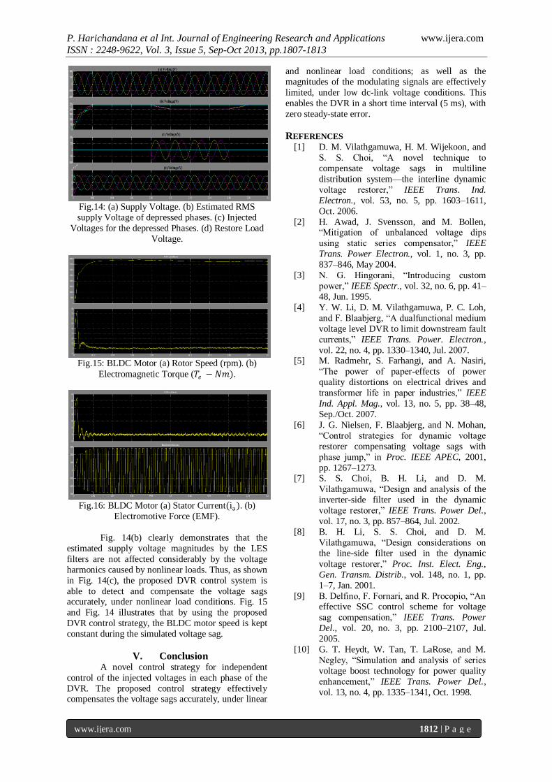
Fig.14: (a) Supply Voltage. (b) Estimated RMS
supply Voltage of depressed phases. (c) Injected
Voltages for the depressed Phases. (d) Restore Load
Voltage.
Fig.15: BLDC Motor (a) Rotor Speed (rpm). (b)
Electromagnetic Torque (𝑇𝑒 − 𝑁𝑚).
Fig.16: BLDC Motor (a) Stator Current(ia). (b)
Electromotive Force (EMF).
Fig. 14(b) clearly demonstrates that the
estimated supply voltage magnitudes by the LES
filters are not affected considerably by the voltage
harmonics caused by nonlinear loads. Thus, as shown
in Fig. 14(c), the proposed DVR control system is
able to detect and compensate the voltage sags accurately, under nonlinear load conditions. Fig. 15
and Fig. 14 illustrates that by using the proposed
DVR control strategy, the BLDC motor speed is kept
constant during the simulated voltage sag.
V. Conclusion A novel control strategy for independent
control of the injected voltages in each phase of the
DVR. The proposed control strategy effectively compensates the voltage sags accurately, under linear
and nonlinear load conditions; as well as the
magnitudes of the modulating signals are effectively
limited, under low dc-link voltage conditions. This
enables the DVR in a short time interval (5 ms), with
zero steady-state error.
REFERENCES [1] D. M. Vilathgamuwa, H. M. Wijekoon, and
S. S. Choi, ―A novel technique to
compensate voltage sags in multiline
distribution system—the interline dynamic
voltage restorer,‖ IEEE Trans. Ind.
Electron., vol. 53, no. 5, pp. 1603–1611,
Oct. 2006.
[2] H. Awad, J. Svensson, and M. Bollen, ―Mitigation of unbalanced voltage dips
using static series compensator,‖ IEEE
Trans. Power Electron., vol. 1, no. 3, pp.
837–846, May 2004.
[3] N. G. Hingorani, ―Introducing custom
power,‖ IEEE Spectr., vol. 32, no. 6, pp. 41–
48, Jun. 1995.
[4] Y. W. Li, D. M. Vilathgamuwa, P. C. Loh,
and F. Blaabjerg, ―A dualfunctional medium
voltage level DVR to limit downstream fault
currents,‖ IEEE Trans. Power. Electron.,
vol. 22, no. 4, pp. 1330–1340, Jul. 2007. [5] M. Radmehr, S. Farhangi, and A. Nasiri,
―The power of paper-effects of power
quality distortions on electrical drives and
transformer life in paper industries,‖ IEEE
Ind. Appl. Mag., vol. 13, no. 5, pp. 38–48,
Sep./Oct. 2007.
[6] J. G. Nielsen, F. Blaabjerg, and N. Mohan,
―Control strategies for dynamic voltage
restorer compensating voltage sags with
phase jump,‖ in Proc. IEEE APEC, 2001,
pp. 1267–1273. [7] S. S. Choi, B. H. Li, and D. M.
Vilathgamuwa, ―Design and analysis of the
inverter-side filter used in the dynamic
voltage restorer,‖ IEEE Trans. Power Del.,
vol. 17, no. 3, pp. 857–864, Jul. 2002.
[8] B. H. Li, S. S. Choi, and D. M.
Vilathgamuwa, ―Design considerations on
the line-side filter used in the dynamic
voltage restorer,‖ Proc. Inst. Elect. Eng.,
Gen. Transm. Distrib., vol. 148, no. 1, pp.
1–7, Jan. 2001.
[9] B. Delfino, F. Fornari, and R. Procopio, ―An effective SSC control scheme for voltage
sag compensation,‖ IEEE Trans. Power
Del., vol. 20, no. 3, pp. 2100–2107, Jul.
2005.
[10] G. T. Heydt, W. Tan, T. LaRose, and M.
Negley, ―Simulation and analysis of series
voltage boost technology for power quality
enhancement,‖ IEEE Trans. Power Del.,
vol. 13, no. 4, pp. 1335–1341, Oct. 1998.

P. Harichandana et al Int. Journal of Engineering Research and Applications www.ijera.com
ISSN : 2248-9622, Vol. 3, Issue 5, Sep-Oct 2013, pp.1807-1813
www.ijera.com 1813 | P a g e
[11] M. J. Newman, D. G. Holmes, J. G. Nielsen,
and F. Blaabjerg, ―A dynamic voltage
restorer (DVR) with selective harmonic
compensation at medium voltage level,‖
IEEE Trans. Ind. Appl., vol. 41, no. 6, pp.
1744–1753, Nov./Dec. 2005. [12] S. S. Choi, T. X. Wang, and D. M.
Vilathgamuwa, ―A series compensator with
fault current limiting functions,‖ IEEE
Trans. Power Del., vol. 20, no. 3, pp. 2248–
2256, Jul. 2005.
[13] V. K. Ramachandaramurthy, C. Fitzer, A.
Arulampalam, C. Zhan, M. Barnes, and N.
Jankins, ―Control of a battery supported
dynamic voltage restorer,‖ Proc. Inst. Elect.
Eng., Gen. Transm. Distrib., vol. 149, no. 5,
pp. 533–542, Sep. 2002.
[14] M. J. Newman, D. G. Holmes, J. G. Nielsen, and F. Blaabjerg, ―A dynamic voltage
restorer (DVR) with selective harmonic
compensation at medium voltage level,‖
IEEE Trans. Ind. Appl., vol. 41, no. 6, pp.
1744–1753, Nov./Dec. 2005.
[15] D. M. Vilathgamuwa, P. C. Loh, and Y. Li,
―Protection of microgrids during utility
voltage sags,‖ IEEE Trans. Ind. Electron.,
vol. 53, no. 5, pp. 1427–1436, Oct. 2006.
Biography
Miss. P. Harichandana
obtained his B.Tech in
Electrical and Electronics
Engineering from QIS
college of Engineering and
Technology, Ongole,
Prakasam, Andhra Pradesh.
She is pursuing M.TECH in Power Electronics and Electrical Drives from
Gudlavalleru Engineering College, Gudlavalleru,
Andhra Pradesh, India. Her areas of interest
include Power Electronics and Electrical
Machines.
Miss. Madhavi sunkara
obtained his B.TECH in
Electrical and Electronics Engineering from Sri
Prakash College of
Engineering, Andhra
Pradesh, India. She received
her M.TECH in Power
Systems from VR Sidhartha Engineerig College,
Andhra Pradesh, India. Her areas of interest
include Power Systems and Power Electronics.
She is currently working as Assistant Professor in
the Electrical and Electronics Engineering
Department in Gudlavalleru Engineering College,
Gudlavalleru, Andhra Pradesh, India.


![PERFORMANCE OF DVR AND IDVR FOR VOLTAGE ...Power Quality Improvement Using Multi -Level Inverter Based DVR and DSTATCOM Using Neuro -Fuzzy Controller. [3] Power Quality Improvement](https://img.pdfslide.net/doc/110x75/5ed31f7b2c1fe74f476f3361/performance-of-dvr-and-idvr-for-voltage-power-quality-improvement-using-multi.jpg)