Embed Size (px)
Citation preview
Process Improvement
Page 1© December 1, 2012 Dr. Lynn Fuller, Professor
Rochester Institute of TechnologyMicroelectronic Engineering
ROCHESTER INSTITUTE OF TECHNOLOGYMICROELECTRONIC ENGINEERING
12-1-2012 Lec_tqm.ppt
Improving Manufacturing Performance
Dr. Lynn FullerWebpage: http://people.rit.edu/~lffeee
Microelectronic EngineeringRochester Institute of Technology
82 Lomb Memorial DriveRochester, NY 14623-5604
Tel (585) 475-2035Fax (585) 475-5041
Email: [email protected] webpage: http://www.microe.rit.edu
This work was supported in part by several programs sponsored by IBMincluding: CIM in Higher Education
TQM Challenge/Award

Process Improvement
Page 2© December 1, 2012 Dr. Lynn Fuller, Professor
Rochester Institute of TechnologyMicroelectronic Engineering
ADOBE PRESENTER
This PowerPoint module has been published using Adobe Presenter. Please click on the Notes tab in the left panel to read the instructors comments for each slide. Manually advance the slide by clicking on the play arrow or pressing the page down key.
Process Improvement
Page 3© December 1, 2012 Dr. Lynn Fuller, Professor
Rochester Institute of TechnologyMicroelectronic Engineering
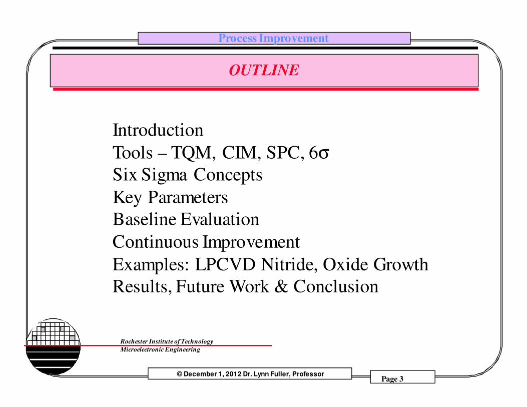
OUTLINE
IntroductionTools – TQM, CIM, SPC, 6σ
Six Sigma ConceptsKey ParametersBaseline EvaluationContinuous ImprovementExamples: LPCVD Nitride, Oxide GrowthResults, Future Work & Conclusion
Process Improvement
Page 4© December 1, 2012 Dr. Lynn Fuller, Professor
Rochester Institute of TechnologyMicroelectronic Engineering
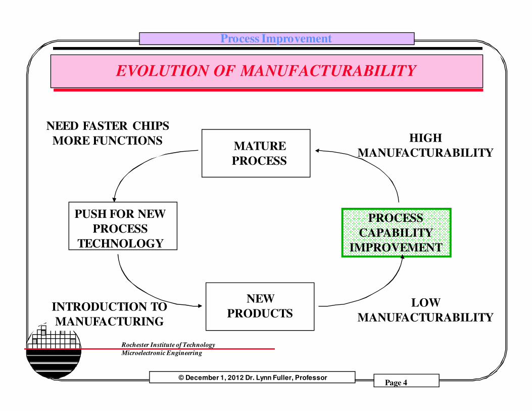
EVOLUTION OF MANUFACTURABILITY
MATURE
PROCESS
PUSH FOR NEW
PROCESS
TECHNOLOGY
NEW
PRODUCTSLOW
MANUFACTURABILITY
HIGH
MANUFACTURABILITY
NEED FASTER CHIPS
MORE FUNCTIONS
INTRODUCTION TO
MANUFACTURING
PROCESS
CAPABILITY
IMPROVEMENT
Process Improvement
Page 5© December 1, 2012 Dr. Lynn Fuller, Professor
Rochester Institute of TechnologyMicroelectronic Engineering
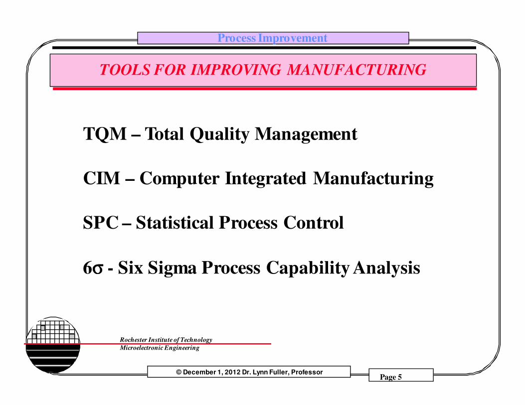
TOOLS FOR IMPROVING MANUFACTURING
TQM – Total Quality Management
CIM – Computer Integrated Manufacturing
SPC – Statistical Process Control
6σσσσ - Six Sigma Process Capability Analysis
Process Improvement
Page 6© December 1, 2012 Dr. Lynn Fuller, Professor
Rochester Institute of TechnologyMicroelectronic Engineering
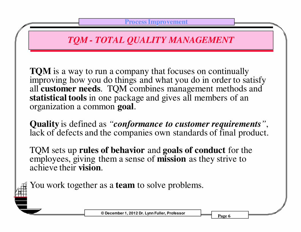
TQM - TOTAL QUALITY MANAGEMENT
TQM is a way to run a company that focuses on continually improving how you do things and what you do in order to satisfy all customer needs. TQM combines management methods and statistical tools in one package and gives all members of an organization a common goal.
Quality is defined as “conformance to customer requirements”, lack of defects and the companies own standards of final product.
TQM sets up rules of behavior and goals of conduct for the employees, giving them a sense of mission as they strive to achieve their vision.
You work together as a team to solve problems.
Process Improvement
Page 7© December 1, 2012 Dr. Lynn Fuller, Professor
Rochester Institute of TechnologyMicroelectronic Engineering
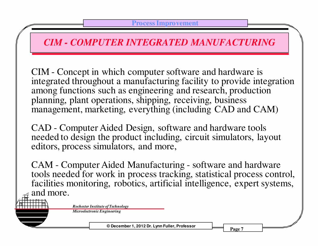
CIM - COMPUTER INTEGRATED MANUFACTURING
CIM - Concept in which computer software and hardware is integrated throughout a manufacturing facility to provide integration among functions such as engineering and research, production planning, plant operations, shipping, receiving, business management, marketing, everything (including CAD and CAM)
CAD - Computer Aided Design, software and hardware tools needed to design the product including, circuit simulators, layout editors, process simulators, and more,
CAM - Computer Aided Manufacturing - software and hardware tools needed for work in process tracking, statistical process control, facilities monitoring, robotics, artificial intelligence, expert systems, and more.
Process Improvement
Page 8© December 1, 2012 Dr. Lynn Fuller, Professor
Rochester Institute of TechnologyMicroelectronic Engineering
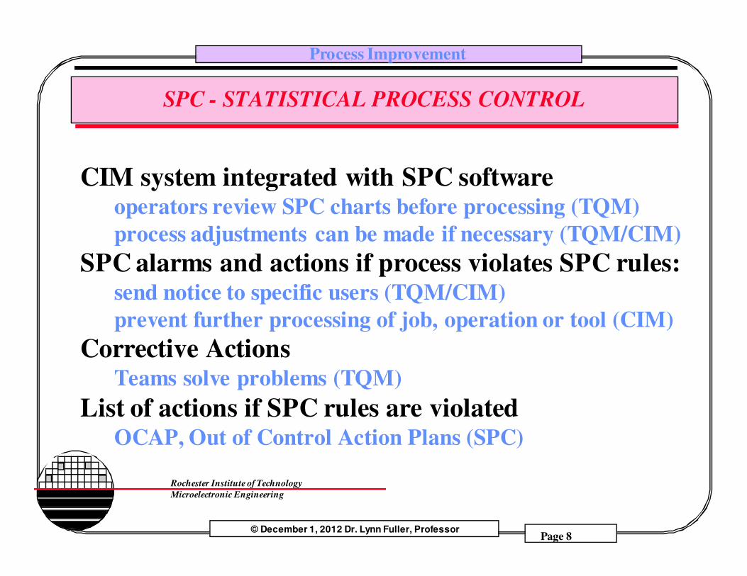
SPC - STATISTICAL PROCESS CONTROL
CIM system integrated with SPC software operators review SPC charts before processing (TQM)
process adjustments can be made if necessary (TQM/CIM)
SPC alarms and actions if process violates SPC rules:send notice to specific users (TQM/CIM)
prevent further processing of job, operation or tool (CIM)
Corrective ActionsTeams solve problems (TQM)
List of actions if SPC rules are violatedOCAP, Out of Control Action Plans (SPC)
Process Improvement
Page 9© December 1, 2012 Dr. Lynn Fuller, Professor
Rochester Institute of TechnologyMicroelectronic Engineering
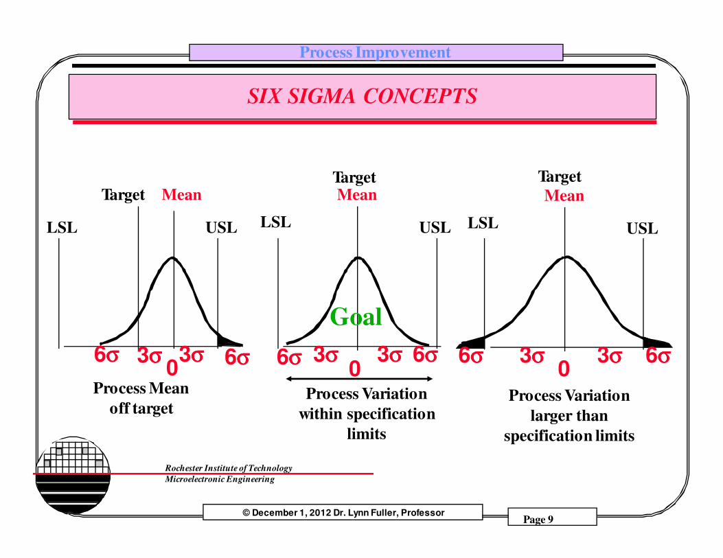
SIX SIGMA CONCEPTS
03σσσσ3σσσσ
LSL USL
Mean
03σσσσ3σσσσ
LSL
Target Mean
USL
03σσσσ3σσσσ
LSL USL
Mean
Process Variation
within specification
limits
Process Variation
larger than
specification limits
Process Mean
off target
6σσσσ 6σσσσ6σσσσ 6σσσσ6σσσσ 6σσσσ
TargetTarget
Goal
Process Improvement
Page 10© December 1, 2012 Dr. Lynn Fuller, Professor
Rochester Institute of TechnologyMicroelectronic Engineering
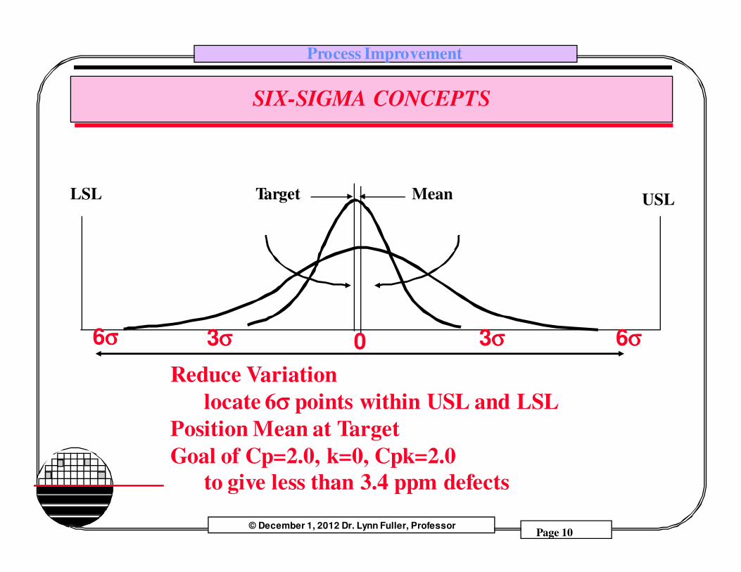
SIX-SIGMA CONCEPTS
0 3σσσσ 6σσσσ3σσσσ6σσσσ
Reduce Variation
locate 6σσσσ points within USL and LSL
Position Mean at Target
Goal of Cp=2.0, k=0, Cpk=2.0
to give less than 3.4 ppm defects
LSL USLTarget Mean
Process Improvement
Page 11© December 1, 2012 Dr. Lynn Fuller, Professor
Rochester Institute of TechnologyMicroelectronic Engineering
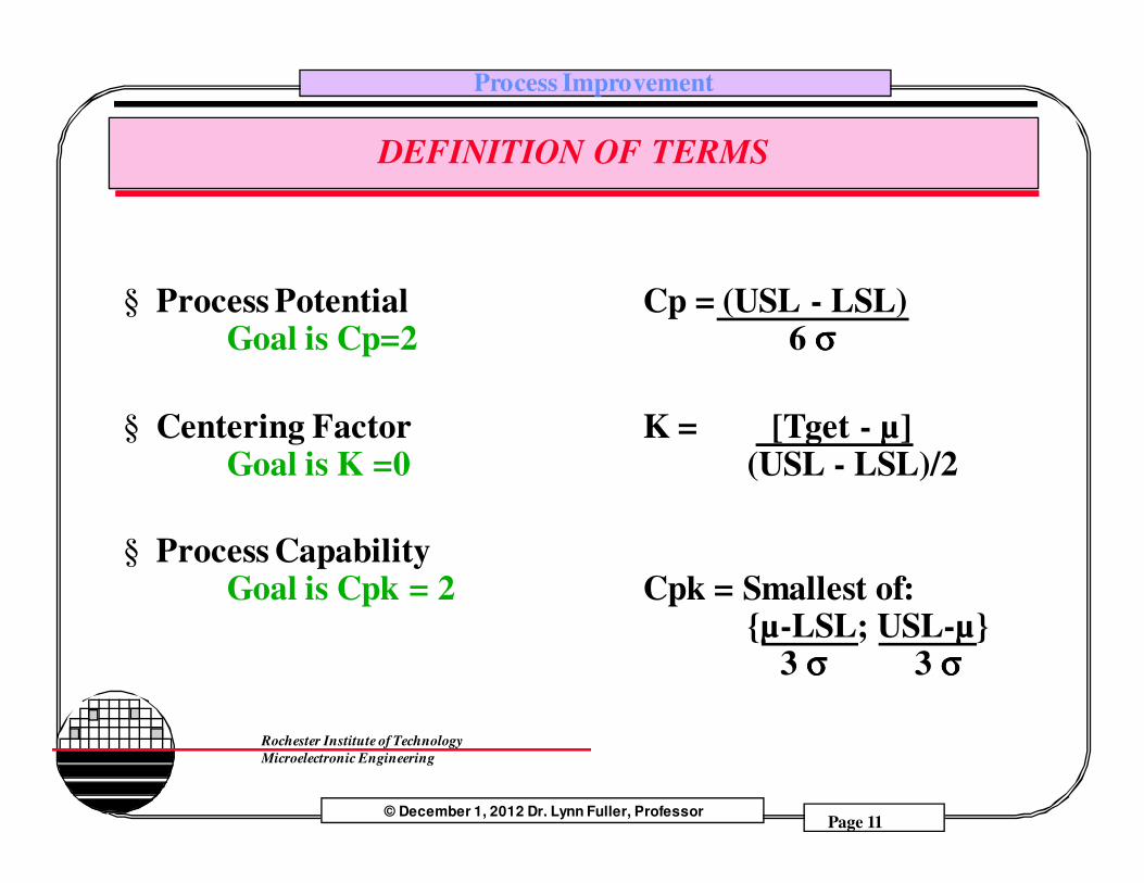
DEFINITION OF TERMS
§ Process Potential Cp = (USL - LSL)Goal is Cp=2 6 σσσσ
§ Centering Factor K = [Tget - µ]Goal is K =0 (USL - LSL)/2
§ Process CapabilityGoal is Cpk = 2 Cpk = Smallest of:
{µ-LSL; USL-µ}3 σσσσ 3 σσσσ
Process Improvement
Page 12© December 1, 2012 Dr. Lynn Fuller, Professor
Rochester Institute of TechnologyMicroelectronic Engineering
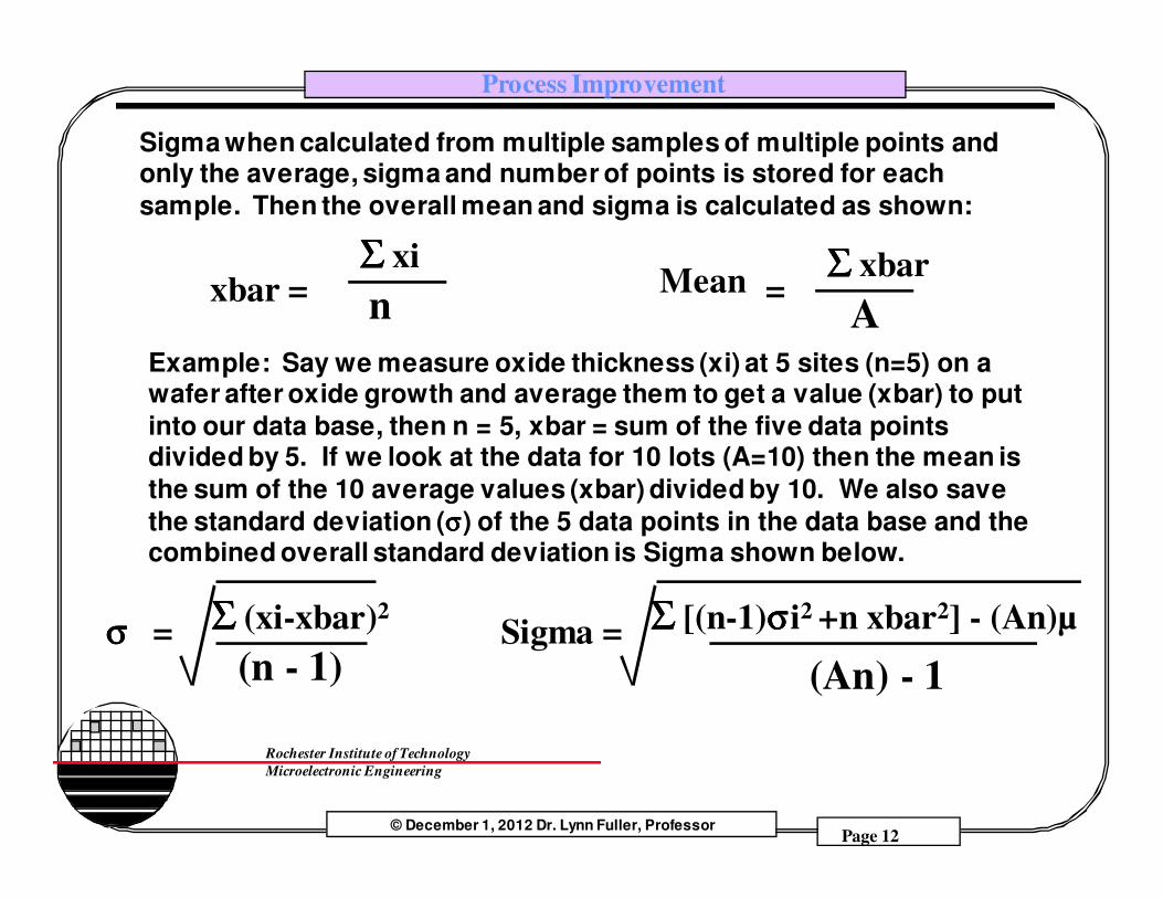
Example: Say we measure oxide thickness (xi) at 5 sites (n=5) on a wafer after oxide growth and average them to get a value (xbar) to put
into our data base, then n = 5, xbar = sum of the five data points divided by 5. If we look at the data for 10 lots (A=10) then the mean is
the sum of the 10 average values (xbar) divided by 10. We also save
the standard deviation (σσσσ) of the 5 data points in the data base and the combined overall standard deviation is Sigma shown below.
n
ΣΣΣΣ xi=
A
ΣΣΣΣ xbar
Sigma =
(An) - 1
ΣΣΣΣ [(n-1)σσσσi2 +n xbar2] - (An)µ
(n - 1)σσσσ = ΣΣΣΣ (xi-xbar)2
Sigma when calculated from multiple samples of multiple points and only the average, sigma and number of points is stored for each
sample. Then the overall mean and sigma is calculated as shown:
Meanxbar =
Process Improvement
Page 13© December 1, 2012 Dr. Lynn Fuller, Professor
Rochester Institute of TechnologyMicroelectronic Engineering
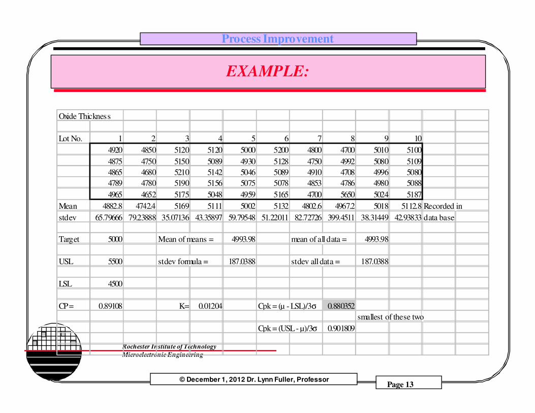
EXAMPLE:
Oxide Thickness
Lot No. 1 2 3 4 5 6 7 8 9 104920 4850 5120 5120 5000 5200 4800 4700 5010 51004875 4750 5150 5089 4930 5128 4750 4992 5080 51094865 4680 5210 5142 5046 5089 4910 4708 4996 50804789 4780 5190 5156 5075 5078 4853 4786 4980 50884965 4652 5175 5048 4959 5165 4700 5650 5024 5187
Mean 4882.8 4742.4 5169 5111 5002 5132 4802.6 4967.2 5018 5112.8 Recorded instdev 65.79666 79.23888 35.07136 43.35897 59.79548 51.22011 82.72726 399.4511 38.31449 42.93833 data base
Target 5000 Mean of means = 4993.98 mean of all data = 4993.98
USL 5500 stdev formula = 187.0388 stdev all data = 187.0388
LSL 4500
CP = 0.89108 K= 0.01204 Cpk = (µ - LSL)/3σ 0.880352smallest of these two
Cpk = (USL - µ)/3σ 0.901809
Process Improvement
Page 14© December 1, 2012 Dr. Lynn Fuller, Professor
Rochester Institute of TechnologyMicroelectronic Engineering
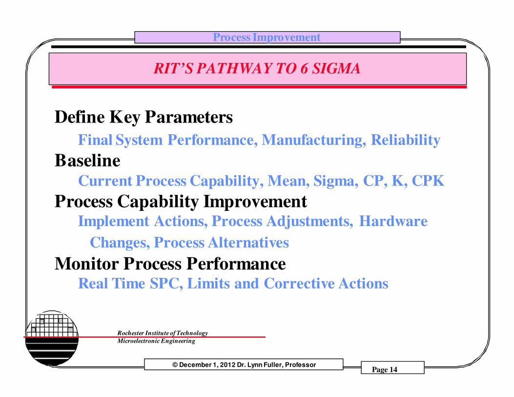
RIT’S PATHWAY TO 6 SIGMA
Define Key Parameters
Final System Performance, Manufacturing, Reliability
BaselineCurrent Process Capability, Mean, Sigma, CP, K, CPK
Process Capability Improvement Implement Actions, Process Adjustments, Hardware
Changes, Process Alternatives
Monitor Process PerformanceReal Time SPC, Limits and Corrective Actions
Process Improvement
Page 15© December 1, 2012 Dr. Lynn Fuller, Professor
Rochester Institute of TechnologyMicroelectronic Engineering
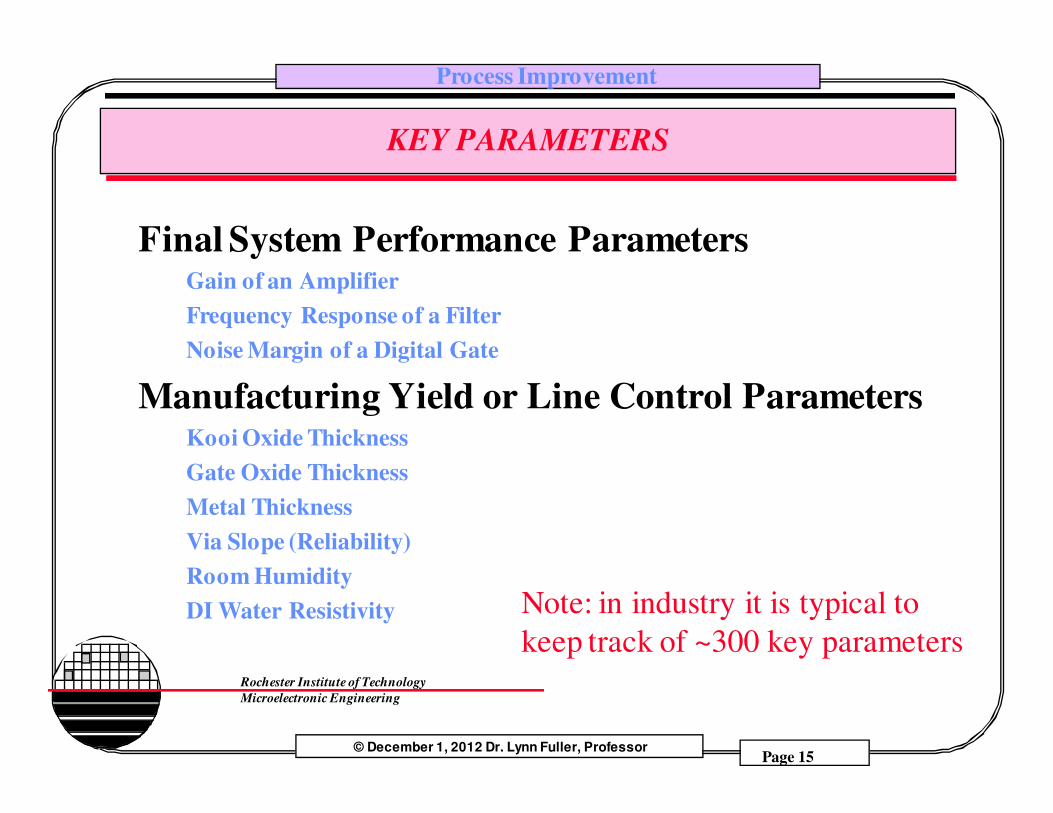
KEY PARAMETERS
Final System Performance ParametersGain of an Amplifier
Frequency Response of a Filter
Noise Margin of a Digital Gate
Manufacturing Yield or Line Control ParametersKooi Oxide Thickness
Gate Oxide Thickness
Metal Thickness
Via Slope (Reliability)
Room Humidity
DI Water Resistivity Note: in industry it is typical tokeep track of ~300 key parameters
Process Improvement
Page 16© December 1, 2012 Dr. Lynn Fuller, Professor
Rochester Institute of TechnologyMicroelectronic Engineering
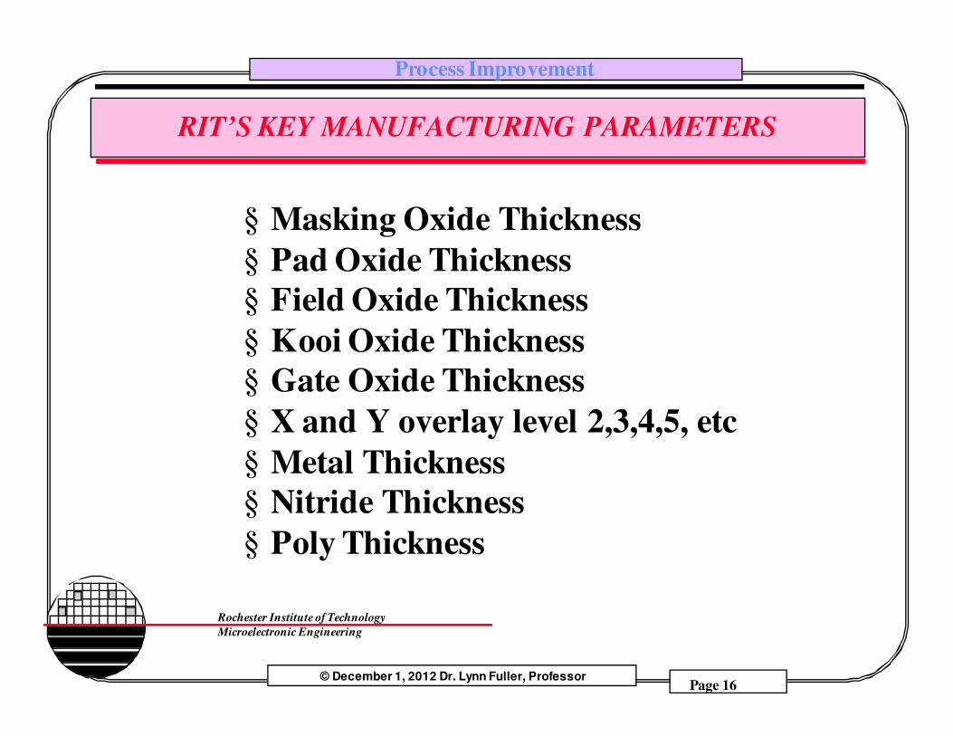
RIT’S KEY MANUFACTURING PARAMETERS
§ Masking Oxide Thickness
§ Pad Oxide Thickness
§ Field Oxide Thickness
§ Kooi Oxide Thickness
§ Gate Oxide Thickness
§ X and Y overlay level 2,3,4,5, etc
§ Metal Thickness
§ Nitride Thickness
§ Poly Thickness
Process Improvement
Page 17© December 1, 2012 Dr. Lynn Fuller, Professor
Rochester Institute of TechnologyMicroelectronic Engineering
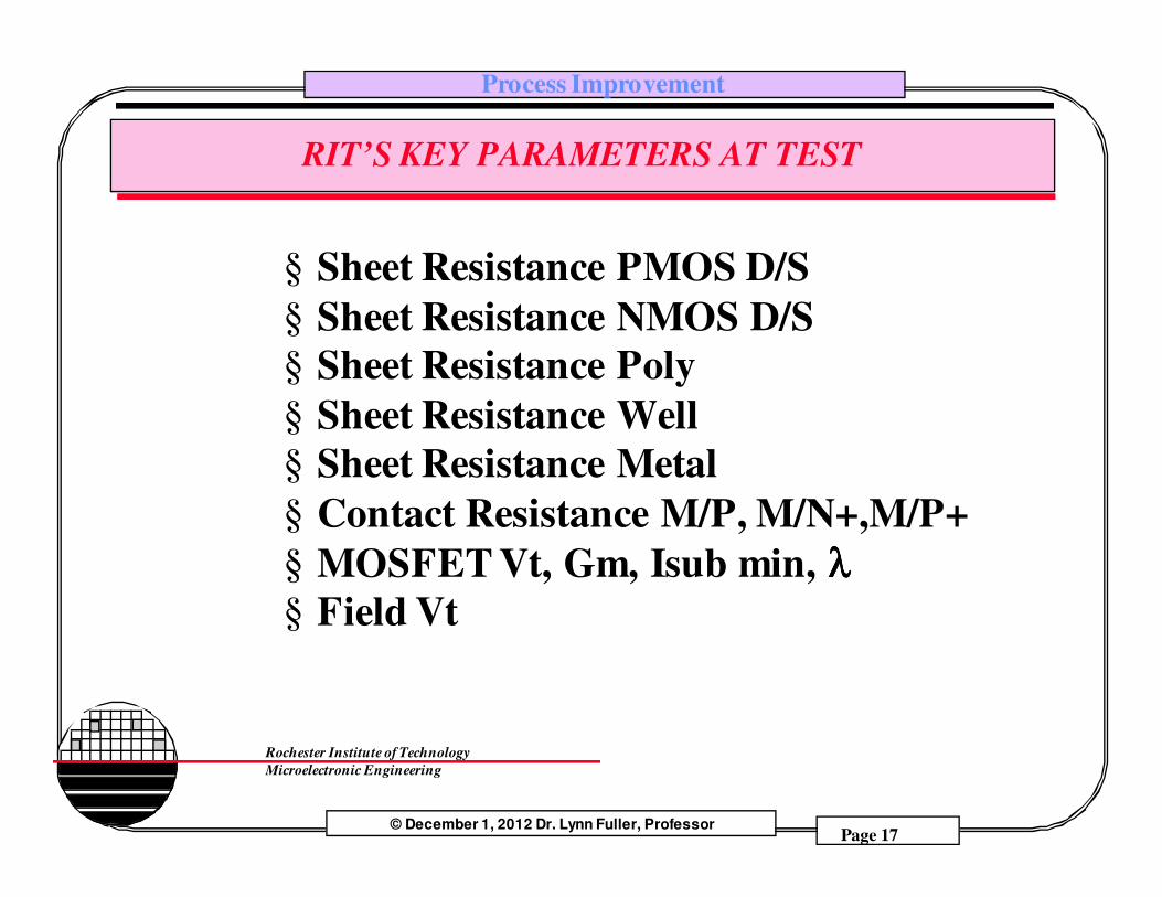
RIT’S KEY PARAMETERS AT TEST
§ Sheet Resistance PMOS D/S
§ Sheet Resistance NMOS D/S
§ Sheet Resistance Poly
§ Sheet Resistance Well
§ Sheet Resistance Metal
§ Contact Resistance M/P, M/N+,M/P+
§ MOSFET Vt, Gm, Isub min, λλλλ
§ Field Vt
Process Improvement
Page 18© December 1, 2012 Dr. Lynn Fuller, Professor
Rochester Institute of TechnologyMicroelectronic Engineering
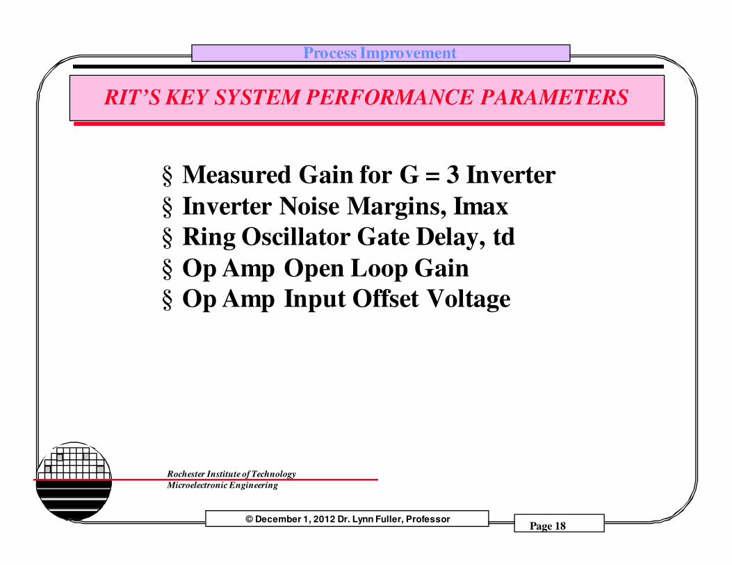
RIT’S KEY SYSTEM PERFORMANCE PARAMETERS
§ Measured Gain for G = 3 Inverter
§ Inverter Noise Margins, Imax
§ Ring Oscillator Gate Delay, td
§ Op Amp Open Loop Gain
§ Op Amp Input Offset Voltage
Process Improvement
Page 19© December 1, 2012 Dr. Lynn Fuller, Professor
Rochester Institute of TechnologyMicroelectronic Engineering
REVIEW OF TARGET, USL AND LSL
The target, USL and LSL for each key parameter is reviewed by a team of engineers using appropriate simulation tools, calculations and experience.
For example: the pad oxide target might be selected to be 1/3 of the nitride thickness for relief of stress in the nitride film (experience). The lower spec is determined by the ability for the pad oxide to act as an etch stop (experience) during nitride plasma etch leaving enough oxide to act as a screening oxide (simulation) for the subsequent ion implant. The upper spec limit is determined by the acceptable amounts of ion implant masking (simulation) and LOCOS birds beak (simulation). All of these are difficult to determine precisely, compromise and margin of error are considered in determining the values for target, USL and LSL.
Process Improvement
Page 20© December 1, 2012 Dr. Lynn Fuller, Professor
Rochester Institute of TechnologyMicroelectronic Engineering
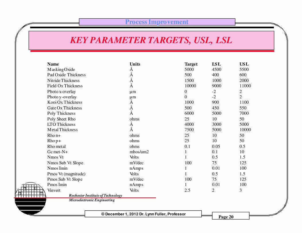
KEY PARAMETER TARGETS, USL, LSL
Name Units Target LSL USL
Masking Oxide Å 5000 4500 5500Pad Oxide Thickness Å 500 400 600Nitride Thickness Å 1500 1000 2000Field Ox Thickness Å 10000 9000 11000Photo x-overlay µm 0 -2 2Photo y-overlay µm 0 -2 2Kooi Ox Thickness Å 1000 900 1100Gate Ox Thickness Å 500 450 550Poly Thickness Å 6000 5000 7000Poly Sheet Rho ohms 25 10 50LTO Thickness Å 4000 3000 5000Metal Thickness Å 7500 5000 10000Rho n+ ohms 25 10 50Rho p+ ohms 25 10 50Rho metal ohms 0.1 0.05 0.5Gc met-N+ mhos/um2 1 0.1 10Nmos Vt Volts 1 0.5 1.5Nmos Sub Vt Slope mV/dec 100 75 125Nmos Imin nAmps 1 0.01 100Pmos Vt (magnitude) Volts 1 0.5 1.5Pmos Sub Vt Slope mV/dec 100 75 125Pmos Imin nAmps 1 0.01 100Vinvert Volts 2.5 2 3
Process Improvement
Page 21© December 1, 2012 Dr. Lynn Fuller, Professor
Rochester Institute of TechnologyMicroelectronic Engineering
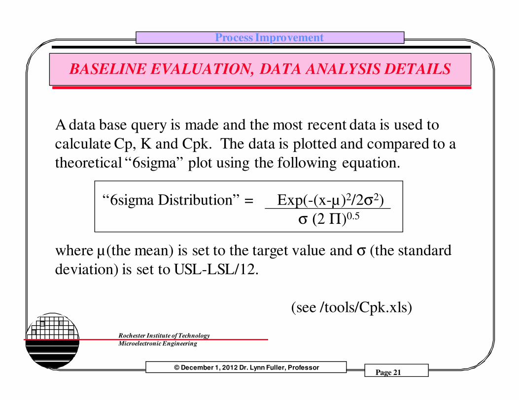
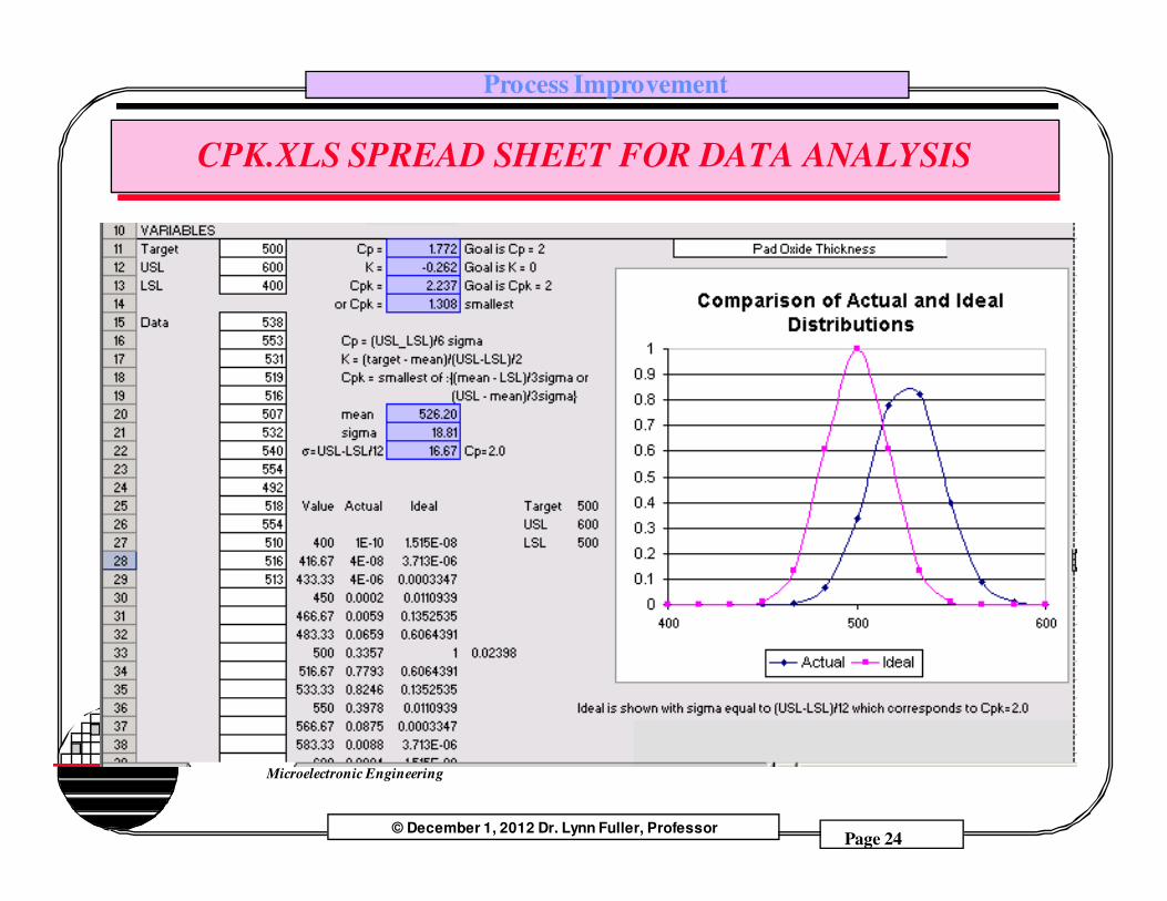
BASELINE EVALUATION, DATA ANALYSIS DETAILS
A data base query is made and the most recent data is used to calculate Cp, K and Cpk. The data is plotted and compared to a theoretical “6sigma” plot using the following equation.
“6sigma Distribution” = Exp(-(x-µ)2/2σ2)σ (2 Π)0.5
where µ(the mean) is set to the target value and σ (the standard deviation) is set to USL-LSL/12.
(see /tools/Cpk.xls)
Process Improvement
Page 22© December 1, 2012 Dr. Lynn Fuller, Professor
Rochester Institute of TechnologyMicroelectronic Engineering
QUERY MESA DATA BASE
Process Improvement
Page 23© December 1, 2012 Dr. Lynn Fuller, Professor
Rochester Institute of TechnologyMicroelectronic Engineering
F5 - REPORT
Process Improvement
Page 24© December 1, 2012 Dr. Lynn Fuller, Professor
Rochester Institute of TechnologyMicroelectronic Engineering
CPK.XLS SPREAD SHEET FOR DATA ANALYSIS
Process Improvement
Page 25© December 1, 2012 Dr. Lynn Fuller, Professor
Rochester Institute of TechnologyMicroelectronic Engineering
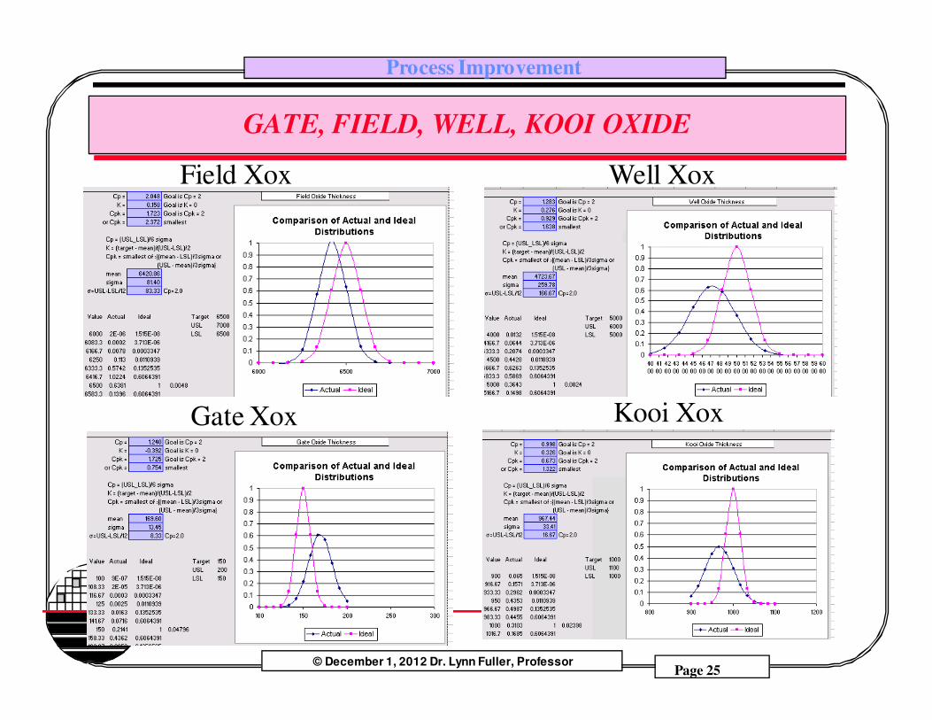
GATE, FIELD, WELL, KOOI OXIDE
Gate Xox
Well Xox
Kooi Xox
Field Xox
Process Improvement
Page 26© December 1, 2012 Dr. Lynn Fuller, Professor
Rochester Institute of TechnologyMicroelectronic Engineering
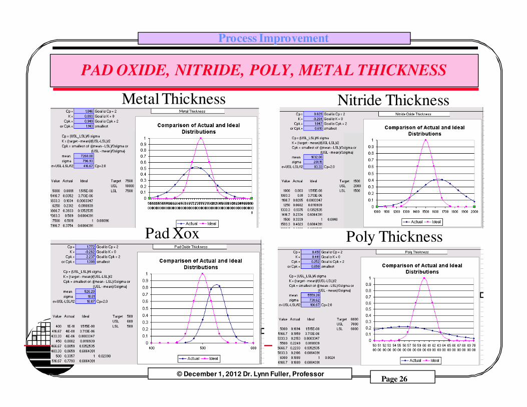
PAD OXIDE, NITRIDE, POLY, METAL THICKNESS
Metal Thickness Nitride Thickness
Poly ThicknessPad Xox
Process Improvement
Page 27© December 1, 2012 Dr. Lynn Fuller, Professor
Rochester Institute of TechnologyMicroelectronic Engineering
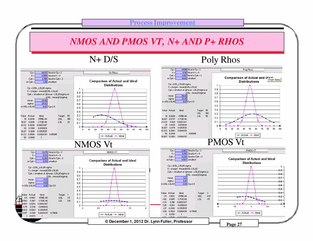
NMOS AND PMOS VT, N+ AND P+ RHOS
PMOS Vt
Poly RhosN+ D/S
NMOS Vt
Process Improvement
Page 28© December 1, 2012 Dr. Lynn Fuller, Professor
Rochester Institute of TechnologyMicroelectronic Engineering
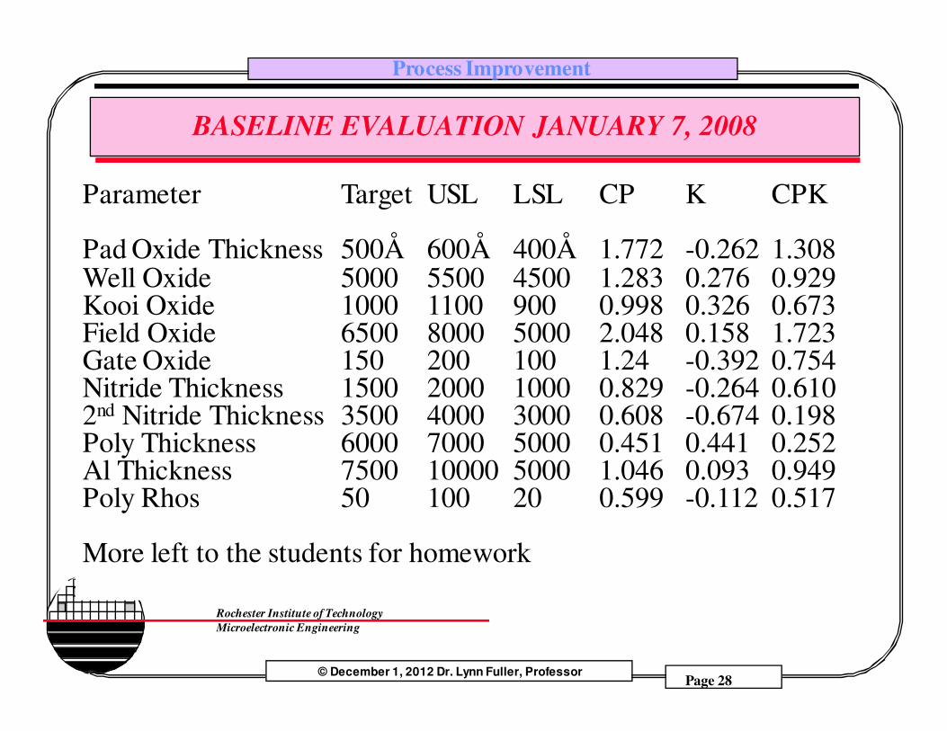
BASELINE EVALUATION JANUARY 7, 2008
Parameter Target USL LSL CP K CPK
Pad Oxide Thickness 500Å 600Å 400Å 1.772 -0.262 1.308Well Oxide 5000 5500 4500 1.283 0.276 0.929Kooi Oxide 1000 1100 900 0.998 0.326 0.673Field Oxide 6500 8000 5000 2.048 0.158 1.723Gate Oxide 150 200 100 1.24 -0.392 0.754Nitride Thickness 1500 2000 1000 0.829 -0.264 0.6102nd Nitride Thickness 3500 4000 3000 0.608 -0.674 0.198Poly Thickness 6000 7000 5000 0.451 0.441 0.252Al Thickness 7500 10000 5000 1.046 0.093 0.949Poly Rhos 50 100 20 0.599 -0.112 0.517
More left to the students for homework
Process Improvement
Page 29© December 1, 2012 Dr. Lynn Fuller, Professor
Rochester Institute of TechnologyMicroelectronic Engineering
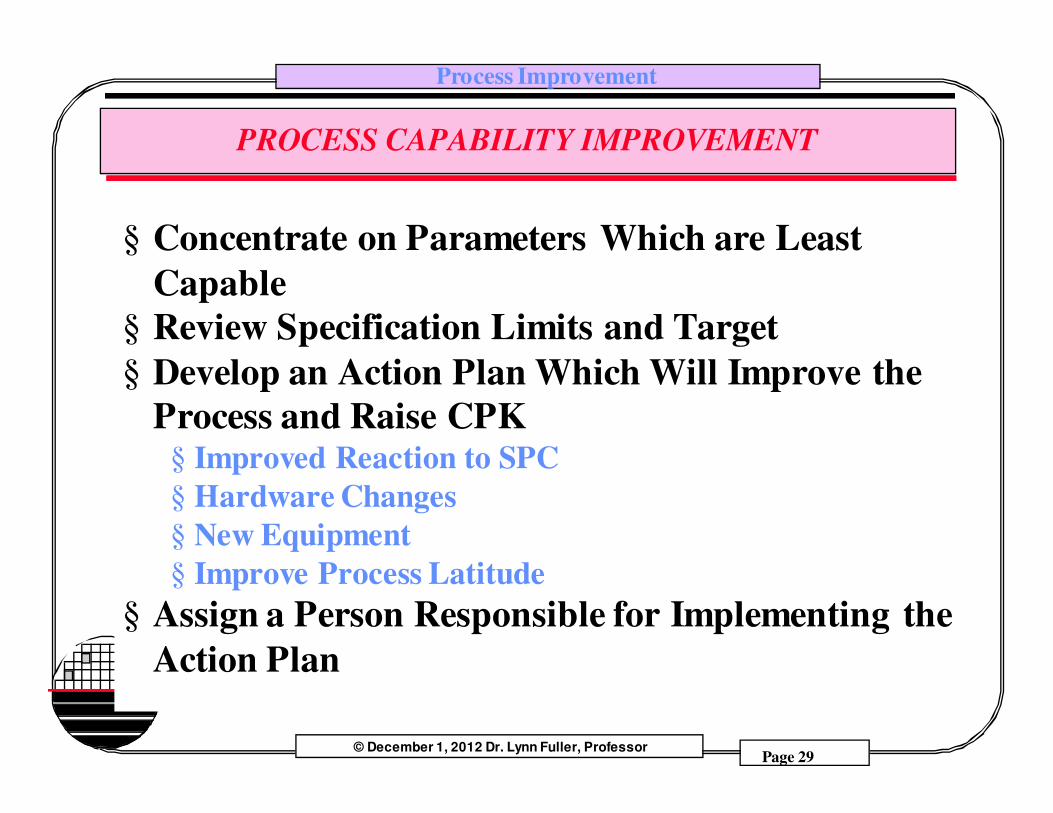
PROCESS CAPABILITY IMPROVEMENT
§ Concentrate on Parameters Which are Least
Capable
§ Review Specification Limits and Target
§ Develop an Action Plan Which Will Improve the
Process and Raise CPK § Improved Reaction to SPC
§ Hardware Changes
§ New Equipment
§ Improve Process Latitude
§ Assign a Person Responsible for Implementing the
Action Plan
Process Improvement
Page 30© December 1, 2012 Dr. Lynn Fuller, Professor
Rochester Institute of TechnologyMicroelectronic Engineering
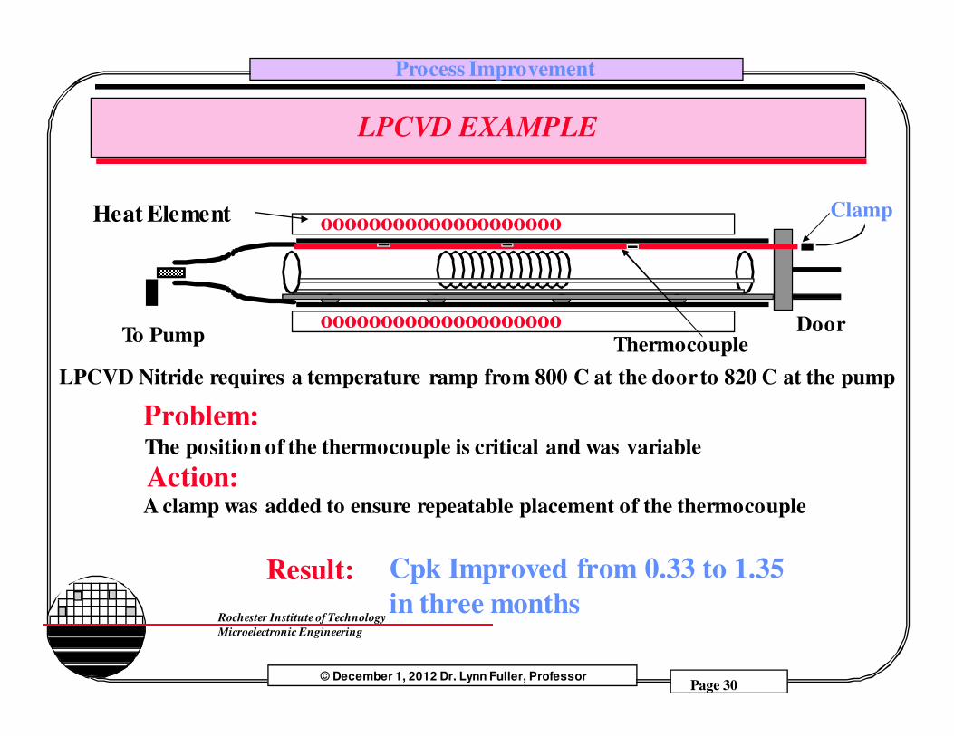
LPCVD EXAMPLE
ClampHeat Element
Thermocouple
LPCVD Nitride requires a temperature ramp from 800 C at the door to 820 C at the pump
The position of the thermocouple is critical and was variable
oooooooooooooooooooo
ooooooooooooooooooooTo Pump
Door
A clamp was added to ensure repeatable placement of the thermocouple
Action:
Problem:
Result: Cpk Improved from 0.33 to 1.35
in three months
Process Improvement
Page 31© December 1, 2012 Dr. Lynn Fuller, Professor
Rochester Institute of TechnologyMicroelectronic Engineering
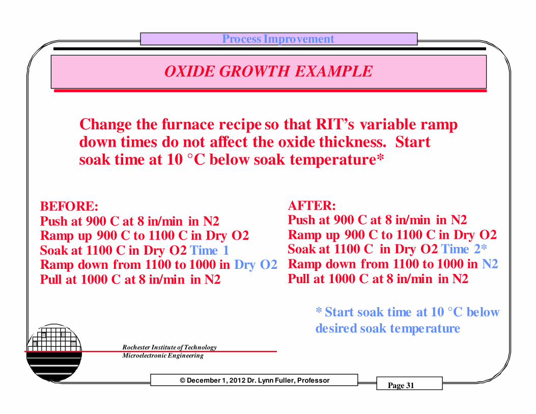
OXIDE GROWTH EXAMPLE
BEFORE:Push at 900 C at 8 in/min in N2Ramp up 900 C to 1100 C in Dry O2Soak at 1100 C in Dry O2 Time 1Ramp down from 1100 to 1000 in Dry O2Pull at 1000 C at 8 in/min in N2
AFTER:Push at 900 C at 8 in/min in N2Ramp up 900 C to 1100 C in Dry O2Soak at 1100 C in Dry O2 Time 2*Ramp down from 1100 to 1000 in N2Pull at 1000 C at 8 in/min in N2
Change the furnace recipe so that RIT’s variable ramp down times do not affect the oxide thickness. Startsoak time at 10 °C below soak temperature*
* Start soak time at 10 °C below
desired soak temperature
Process Improvement
Page 32© December 1, 2012 Dr. Lynn Fuller, Professor
Rochester Institute of TechnologyMicroelectronic Engineering
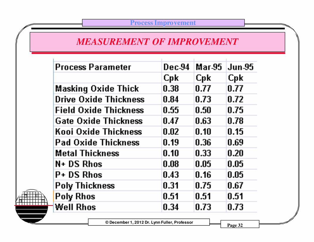
MEASUREMENT OF IMPROVEMENT
Process Improvement
Page 33© December 1, 2012 Dr. Lynn Fuller, Professor
Rochester Institute of TechnologyMicroelectronic Engineering
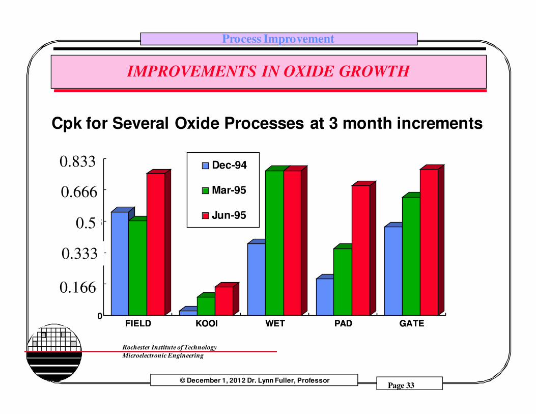
IMPROVEMENTS IN OXIDE GROWTH
FIELD KOOI WET PAD GATE0
0.5
1
1.5
2
2.5
FIELD KOOI WET PAD GATE
Dec-94
Mar-95
Jun-95
Cpk for Several Oxide Processes at 3 month increments
0.333
0.833
0.5
0.166
0.666
Process Improvement
Page 34© December 1, 2012 Dr. Lynn Fuller, Professor
Rochester Institute of TechnologyMicroelectronic Engineering
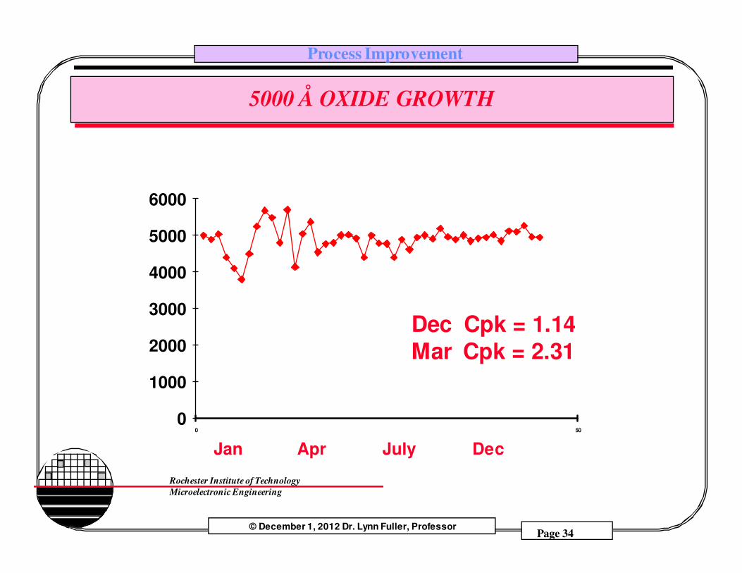
5000 Å OXIDE GROWTH
0
1000
2000
3000
4000
5000
6000
0 50
Jan Apr July Dec
Dec Cpk = 1.14
Mar Cpk = 2.31
Process Improvement
Page 35© December 1, 2012 Dr. Lynn Fuller, Professor
Rochester Institute of TechnologyMicroelectronic Engineering
MONITOR PROCESS PERFORMANCE WITH SPC
Mesa data base queries are run that put the results into a data file.
Using the data in the data file, SPC charts are created by “NWA Quality Analyst Software” or other appropriate software.
Tool operators are taught how to evaluate the SPC charts for out of control criteria and what to do if the data shows an out of control condition (OCAP).
SPC alarms can automatically send notice to specific users and prevent further processing of job, operation or tool.
Teams evaluate and correct the problem.
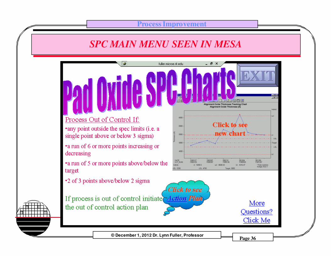
Process Improvement
Page 36© December 1, 2012 Dr. Lynn Fuller, Professor
Rochester Institute of TechnologyMicroelectronic Engineering
SPC MAIN MENU SEEN IN MESA
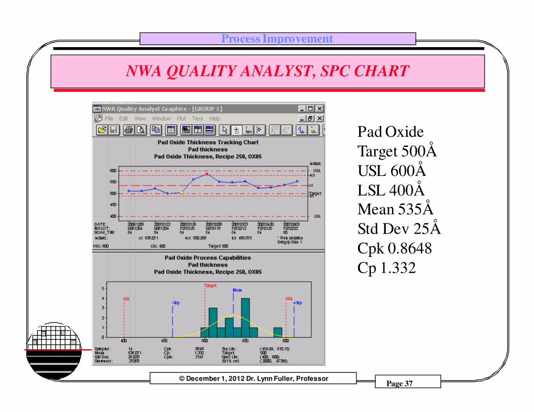
Process Improvement
Page 37© December 1, 2012 Dr. Lynn Fuller, Professor
Rochester Institute of TechnologyMicroelectronic Engineering
NWA QUALITY ANALYST, SPC CHART
Pad OxideTarget 500ÅUSL 600ÅLSL 400ÅMean 535ÅStd Dev 25ÅCpk 0.8648Cp 1.332
Process Improvement
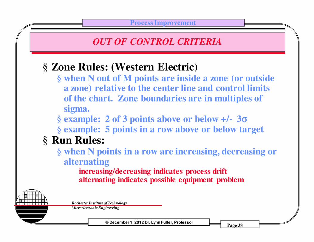
Page 38© December 1, 2012 Dr. Lynn Fuller, Professor
Rochester Institute of TechnologyMicroelectronic Engineering
OUT OF CONTROL CRITERIA
§ Zone Rules: (Western Electric)§ when N out of M points are inside a zone (or outside
a zone) relative to the center line and control limits of the chart. Zone boundaries are in multiples of sigma.
§ example: 2 of 3 points above or below +/- 3σσσσ§ example: 5 points in a row above or below target
§ Run Rules:§ when N points in a row are increasing, decreasing or
alternating increasing/decreasing indicates process drift alternating indicates possible equipment problem
Process Improvement
Page 39© December 1, 2012 Dr. Lynn Fuller, Professor
Rochester Institute of TechnologyMicroelectronic Engineering
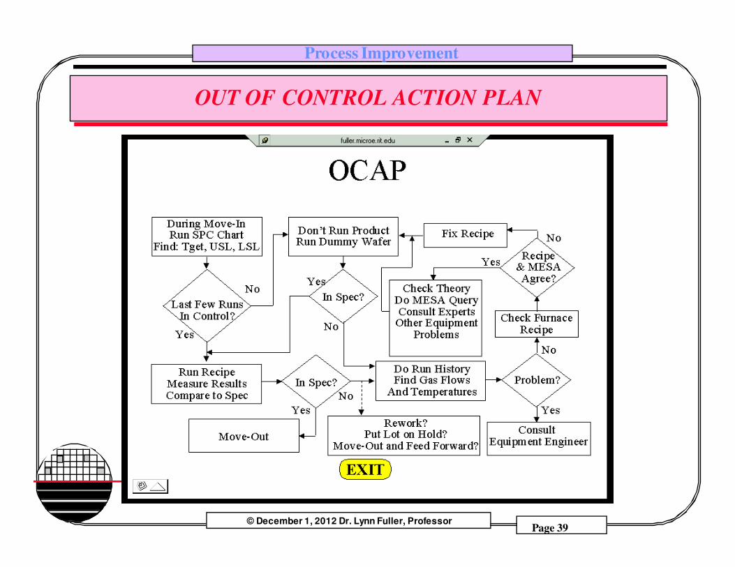
OUT OF CONTROL ACTION PLAN
Process Improvement
Page 40© December 1, 2012 Dr. Lynn Fuller, Professor
Rochester Institute of TechnologyMicroelectronic Engineering
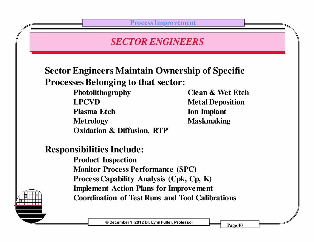
SECTOR ENGINEERS
Sector Engineers Maintain Ownership of Specific
Processes Belonging to that sector:Photolithography Clean & Wet Etch
LPCVD Metal Deposition
Plasma Etch Ion Implant
Metrology Maskmaking
Oxidation & Diffusion, RTP
Responsibilities Include:Product Inspection
Monitor Process Performance (SPC)
Process Capability Analysis (Cpk, Cp, K)
Implement Action Plans for Improvement
Coordination of Test Runs and Tool Calibrations
Process Improvement
Page 41© December 1, 2012 Dr. Lynn Fuller, Professor
Rochester Institute of TechnologyMicroelectronic Engineering
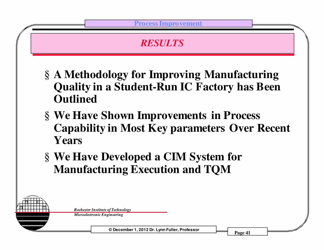
RESULTS
§ A Methodology for Improving Manufacturing Quality in a Student-Run IC Factory has Been Outlined
§ We Have Shown Improvements in Process Capability in Most Key parameters Over Recent Years
§ We Have Developed a CIM System for Manufacturing Execution and TQM
Process Improvement
Page 42© December 1, 2012 Dr. Lynn Fuller, Professor
Rochester Institute of TechnologyMicroelectronic Engineering
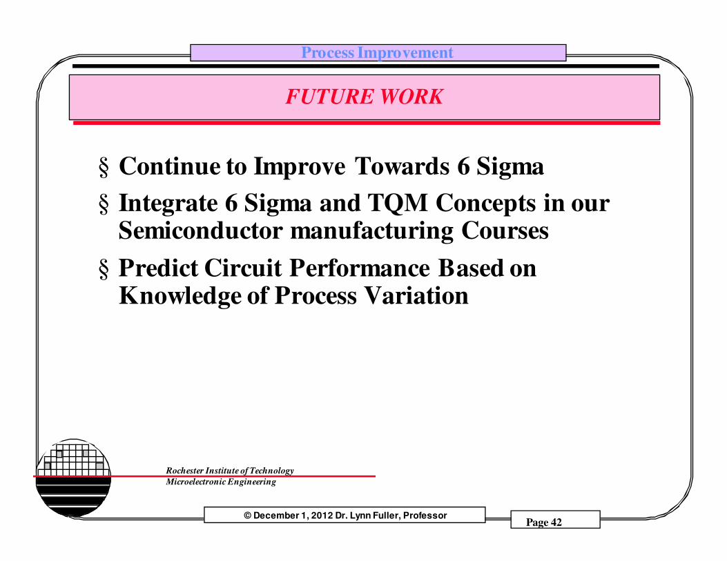
FUTURE WORK
§ Continue to Improve Towards 6 Sigma
§ Integrate 6 Sigma and TQM Concepts in our Semiconductor manufacturing Courses
§ Predict Circuit Performance Based on Knowledge of Process Variation
Process Improvement
Page 43© December 1, 2012 Dr. Lynn Fuller, Professor
Rochester Institute of TechnologyMicroelectronic Engineering
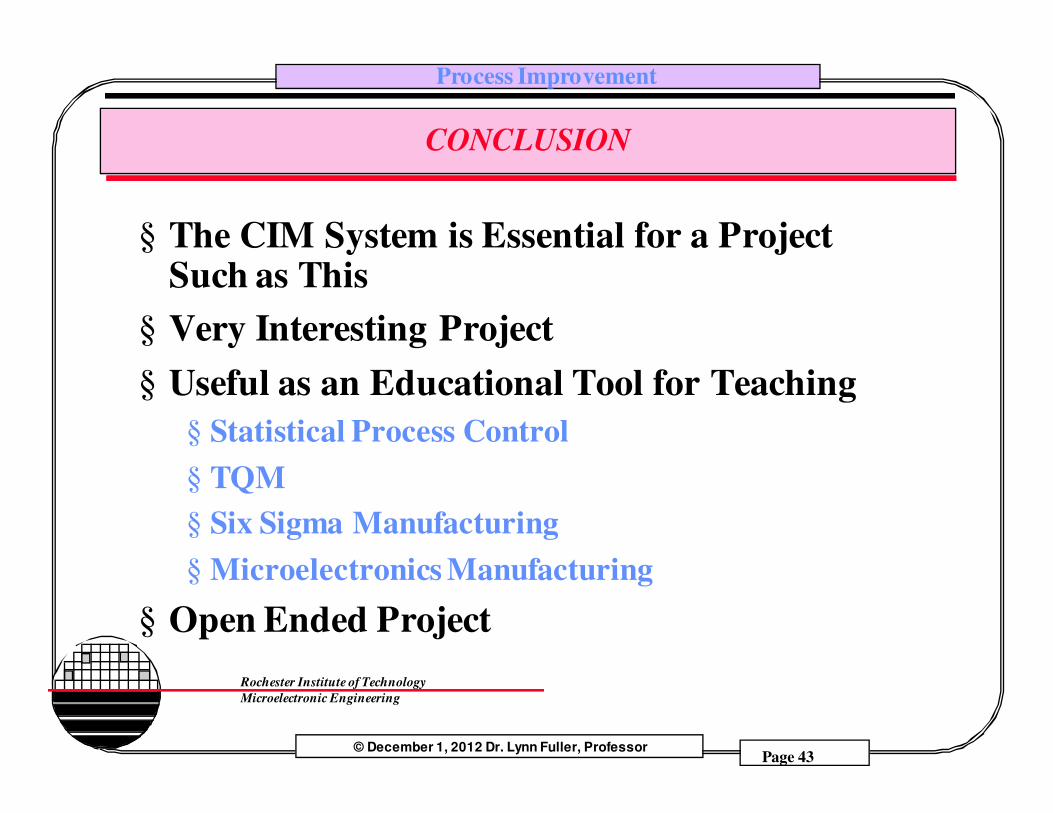
CONCLUSION
§ The CIM System is Essential for a Project Such as This
§ Very Interesting Project
§ Useful as an Educational Tool for Teaching
§ Statistical Process Control
§ TQM
§ Six Sigma Manufacturing
§ Microelectronics Manufacturing
§ Open Ended Project
Process Improvement
Page 44© December 1, 2012 Dr. Lynn Fuller, Professor
Rochester Institute of TechnologyMicroelectronic Engineering
REFERENCES
1. Western Electric Guide to Quality Control2. “Control Chart Techniques for High Volume, Multiple Process Wafer Fabrication Areas”, Tom Bassett III, Signeteics Corp., IEEE/SEMI Advanced Semiconductor Manufacturing Conference, 1991.
Process Improvement
Page 45© December 1, 2012 Dr. Lynn Fuller, Professor
Rochester Institute of TechnologyMicroelectronic Engineering
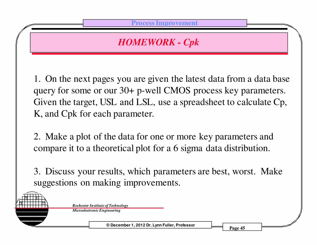
HOMEWORK - Cpk
1. On the next pages you are given the latest data from a data base query for some or our 30+ p-well CMOS process key parameters. Given the target, USL and LSL, use a spreadsheet to calculate Cp, K, and Cpk for each parameter.
2. Make a plot of the data for one or more key parameters and compare it to a theoretical plot for a 6 sigma data distribution.
3. Discuss your results, which parameters are best, worst. Make suggestions on making improvements.
Process Improvement
Page 46© December 1, 2012 Dr. Lynn Fuller, Professor
Rochester Institute of TechnologyMicroelectronic Engineering
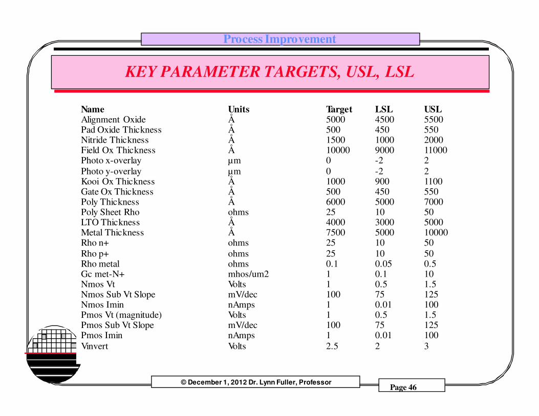
KEY PARAMETER TARGETS, USL, LSL
Name Units Target LSL USLAlignment Oxide Å 5000 4500 5500Pad Oxide Thickness Å 500 450 550Nitride Thickness Å 1500 1000 2000Field Ox Thickness Å 10000 9000 11000Photo x-overlay µm 0 -2 2Photo y-overlay µm 0 -2 2Kooi Ox Thickness Å 1000 900 1100Gate Ox Thickness Å 500 450 550Poly Thickness Å 6000 5000 7000Poly Sheet Rho ohms 25 10 50LTO Thickness Å 4000 3000 5000Metal Thickness Å 7500 5000 10000Rho n+ ohms 25 10 50Rho p+ ohms 25 10 50Rho metal ohms 0.1 0.05 0.5Gc met-N+ mhos/um2 1 0.1 10Nmos Vt Volts 1 0.5 1.5Nmos Sub Vt Slope mV/dec 100 75 125Nmos Imin nAmps 1 0.01 100Pmos Vt (magnitude) Volts 1 0.5 1.5Pmos Sub Vt Slope mV/dec 100 75 125Pmos Imin nAmps 1 0.01 100Vinvert Volts 2.5 2 3
Process Improvement
Page 47© December 1, 2012 Dr. Lynn Fuller, Professor
Rochester Institute of TechnologyMicroelectronic Engineering
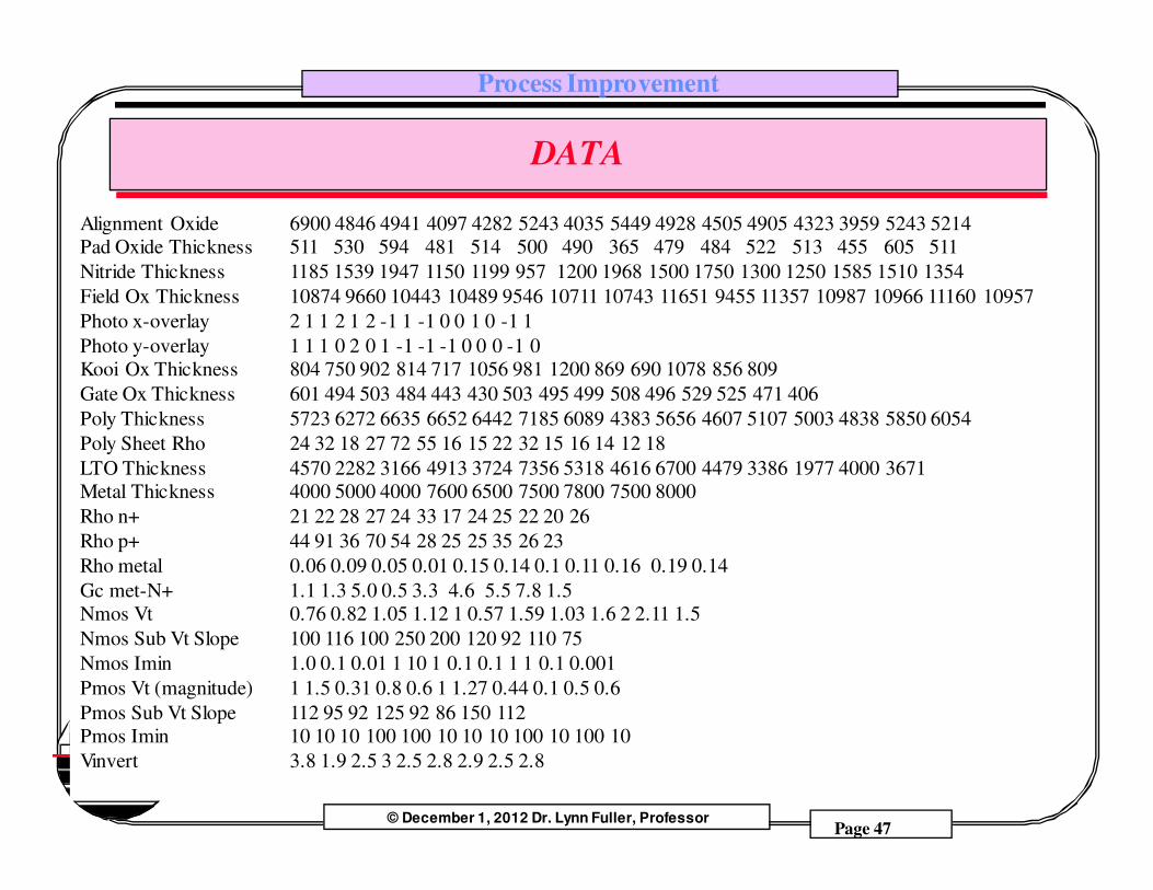
DATA
Alignment Oxide 6900 4846 4941 4097 4282 5243 4035 5449 4928 4505 4905 4323 3959 5243 5214Pad Oxide Thickness 511 530 594 481 514 500 490 365 479 484 522 513 455 605 511 Nitride Thickness 1185 1539 1947 1150 1199 957 1200 1968 1500 1750 1300 1250 1585 1510 1354Field Ox Thickness 10874 9660 10443 10489 9546 10711 10743 11651 9455 11357 10987 10966 11160 10957 Photo x-overlay 2 1 1 2 1 2 -1 1 -1 0 0 1 0 -1 1Photo y-overlay 1 1 1 0 2 0 1 -1 -1 -1 0 0 0 -1 0Kooi Ox Thickness 804 750 902 814 717 1056 981 1200 869 690 1078 856 809Gate Ox Thickness 601 494 503 484 443 430 503 495 499 508 496 529 525 471 406Poly Thickness 5723 6272 6635 6652 6442 7185 6089 4383 5656 4607 5107 5003 4838 5850 6054Poly Sheet Rho 24 32 18 27 72 55 16 15 22 32 15 16 14 12 18LTO Thickness 4570 2282 3166 4913 3724 7356 5318 4616 6700 4479 3386 1977 4000 3671Metal Thickness 4000 5000 4000 7600 6500 7500 7800 7500 8000 Rho n+ 21 22 28 27 24 33 17 24 25 22 20 26Rho p+ 44 91 36 70 54 28 25 25 35 26 23Rho metal 0.06 0.09 0.05 0.01 0.15 0.14 0.1 0.11 0.16 0.19 0.14Gc met-N+ 1.1 1.3 5.0 0.5 3.3 4.6 5.5 7.8 1.5 Nmos Vt 0.76 0.82 1.05 1.12 1 0.57 1.59 1.03 1.6 2 2.11 1.5Nmos Sub Vt Slope 100 116 100 250 200 120 92 110 75 Nmos Imin 1.0 0.1 0.01 1 10 1 0.1 0.1 1 1 0.1 0.001Pmos Vt (magnitude) 1 1.5 0.31 0.8 0.6 1 1.27 0.44 0.1 0.5 0.6Pmos Sub Vt Slope 112 95 92 125 92 86 150 112 Pmos Imin 10 10 10 100 100 10 10 10 100 10 100 10Vinvert 3.8 1.9 2.5 3 2.5 2.8 2.9 2.5 2.8