Embed Size (px)
Citation preview
White Paper by Measurement Computing, Inc.©Copyright 2013 Measurement Computing, Inc.
Data Acquisition Fundamentals: Improving Measurement Quality with Signal Conditioning
Page 2 Measurement Computing | 1-800-234-4232 | [email protected] | mccdaq.com
Introduction
When measuring real-world physical phenomenon, signal conditioning is a prerequisite for correctly processing the electrical signals from the sensor and improving the overall quality of the data. Just as wheat grown in the field requires much processing before appearing as bags of flour in the grocery store, raw signals must be cleaned up, transformed, and properly adjusted to become a usable output that humans and machines can understand.
Different types of signal conditioning should be selected, depending on the type of measurement and data acquisition device being used. To familiarize you with the basics of signal conditioning, this white paper defines and discusses the most common types used in data acquisition: • Analogfront-endtopology• Instrumentationamplifiers• Filtering• Attenuation• Isolation• Linearization• Circuitprotection
Each technique has its benefits and limitations. This document seeks to explain the best practices and most common use cases. Circuit diagrams and equations describe how to select the correct components. Understanding the unique characteristics of these signal conditioning methods will help improve the measurement accuracy of your data acquisition system.
Analog Front-End Topology
Data acquisition systems differ from single- or dual-channel instruments in several ways. They can measure and store data collected from hundreds of channels simultaneously. However, most systems contain from eight to 32 channels, typically in multiples of eight. By comparison, a simple voltmeter that selects a measurement among several different ranges can be considered
Data Acquisition Architecture
Page 3 Measurement Computing | 1-800-234-4232 | [email protected] | mccdaq.com
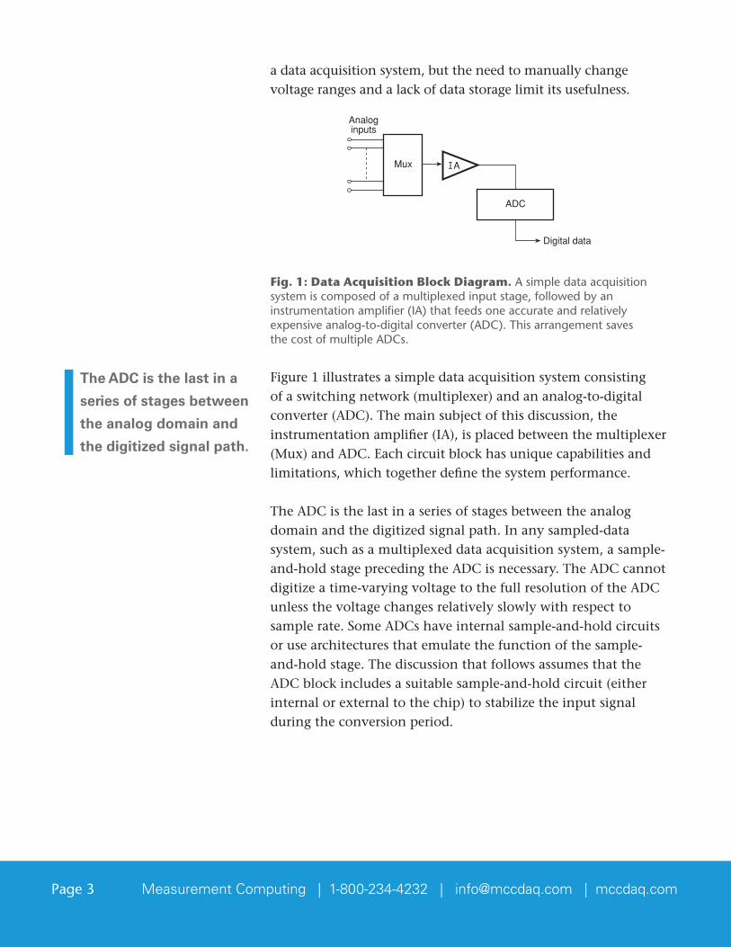
a data acquisition system, but the need to manually change voltage ranges and a lack of data storage limit its usefulness.
Figure 5.01
Analoginputs
IA
ADC
Mux
Digital data
Fig. 1: Data Acquisition Block Diagram. A simple data acquisition system is composed of a multiplexed input stage, followed by an instrumentation amplifier (IA) that feeds one accurate and relatively expensive analog-to-digital converter (ADC). This arrangement saves the cost of multiple ADCs.
Figure1illustratesasimpledataacquisitionsystemconsistingof a switching network (multiplexer) and an analog-to-digital converter(ADC).Themainsubjectofthisdiscussion,theinstrumentationamplifier(IA),isplacedbetweenthemultiplexer(Mux)andADC.Eachcircuitblockhasuniquecapabilitiesandlimitations, which together define the system performance.
TheADCisthelastinaseriesofstagesbetweentheanalogdomain and the digitized signal path. In any sampled-data system, such as a multiplexed data acquisition system, a sample-and-holdstageprecedingtheADCisnecessary.TheADCcannotdigitizeatime-varyingvoltagetothefullresolutionoftheADCunless the voltage changes relatively slowly with respect to samplerate.SomeADCshaveinternalsample-and-holdcircuitsor use architectures that emulate the function of the sample-and-hold stage. The discussion that follows assumes that the ADCblockincludesasuitablesample-and-holdcircuit(eitherinternal or external to the chip) to stabilize the input signal during the conversion period.
The ADC is the last in a
series of stages between
the analog domain and
the digitized signal path.
Page 4 Measurement Computing | 1-800-234-4232 | [email protected] | mccdaq.com
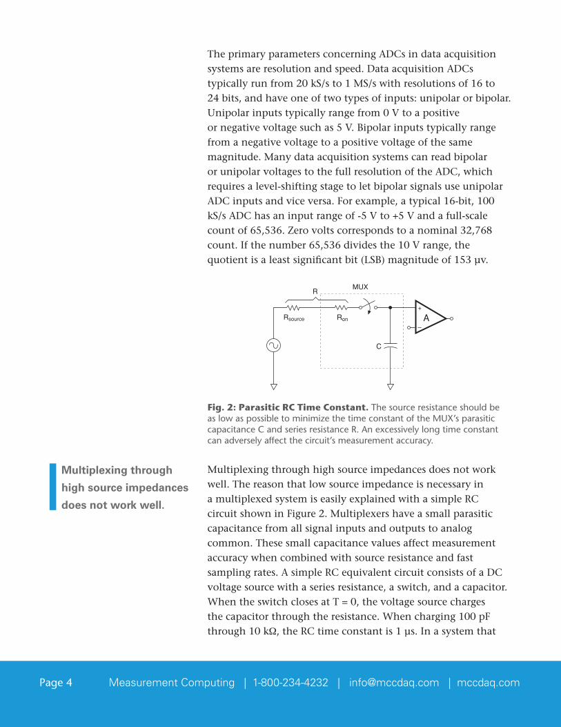
TheprimaryparametersconcerningADCsindataacquisitionsystemsareresolutionandspeed.DataacquisitionADCstypicallyrunfrom20kS/sto1MS/swithresolutionsof16to 24 bits, and have one of two types of inputs: unipolar or bipolar. Unipolar inputs typically range from 0 V to a positive or negative voltage such as 5 V. Bipolar inputs typically range from a negative voltage to a positive voltage of the same magnitude. Many data acquisition systems can read bipolar orunipolarvoltagestothefullresolutionoftheADC,whichrequires a level-shifting stage to let bipolar signals use unipolar ADCinputsandviceversa.Forexample,atypical16-bit,100kS/sADChasaninputrangeof-5Vto+5Vandafull-scalecountof65,536.Zerovoltscorrespondstoanominal32,768count.Ifthenumber65,536dividesthe10Vrange,thequotientisaleastsignificantbit(LSB)magnitudeof153μv.
Figure 5.02
Rsource Ron A+
–
MUXR
C
Fig. 2: Parasitic RC Time Constant. The source resistance should be as low as possible to minimize the time constant of the MUX’s parasitic capacitance C and series resistance R. An excessively long time constant can adversely affect the circuit’s measurement accuracy.
Multiplexing through high source impedances does not work well. The reason that low source impedance is necessary in a multiplexed system is easily explained with a simple RC circuitshowninFigure2.Multiplexershaveasmallparasiticcapacitance from all signal inputs and outputs to analog common. These small capacitance values affect measurement accuracy when combined with source resistance and fast samplingrates.AsimpleRCequivalentcircuitconsistsofaDCvoltage source with a series resistance, a switch, and a capacitor. When the switch closes at T = 0, the voltage source charges thecapacitorthroughtheresistance.Whencharging100pFthrough10kΩ,theRCtimeconstantis1μs.Inasystemthat
Multiplexing through
high source impedances
does not work well.
Page 5 Measurement Computing | 1-800-234-4232 | [email protected] | mccdaq.com
has2μsavailableforsettlingtime,thecapacitoronlychargesto86%ofthevalueoftheinput,whichintroducesa14%error.Changingthe10kΩresistortoa1kΩ resistor lets the capacitor easily charge to an accurate value in 20 time constants.
Figure 5.03 A
Rs
Ri
Transducer
Vsig
VADC = VsigRi
Rs + Ri
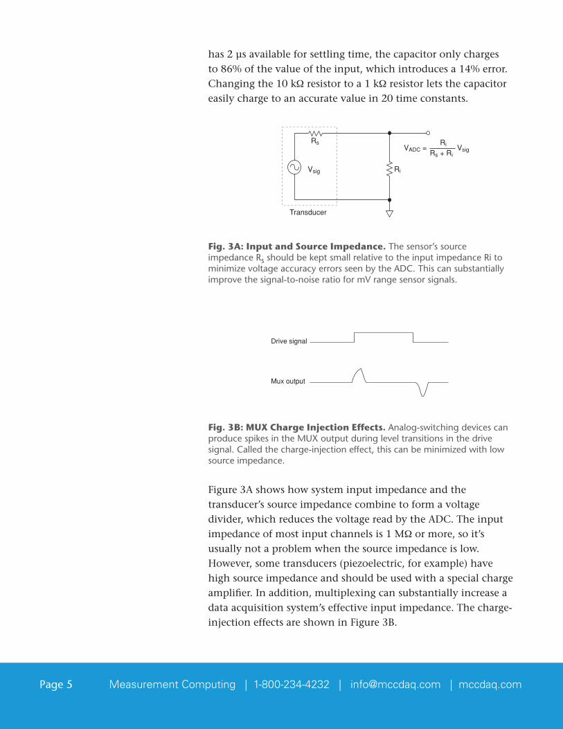
Fig. 3A: Input and Source Impedance. The sensor’s source impedance Rs should be kept small relative to the input impedance Ri to minimize voltage accuracy errors seen by the ADC. This can substantially improve the signal-to-noise ratio for mV range sensor signals.
Drive signal
Mux output
Figure 5.03 B
Fig. 3B: MUX Charge Injection Effects. Analog-switching devices can produce spikes in the MUX output during level transitions in the drive signal. Called the charge-injection effect, this can be minimized with low source impedance.
Figure3Ashowshowsysteminputimpedanceandthetransducer’s source impedance combine to form a voltage divider,whichreducesthevoltagereadbytheADC.Theinputimpedanceofmostinputchannelsis1MΩ or more, so it’s usually not a problem when the source impedance is low. However, some transducers (piezoelectric, for example) have high source impedance and should be used with a special charge amplifier. In addition, multiplexing can substantially increase a data acquisition system’s effective input impedance. The charge-injectioneffectsareshowninFigure3B.
Page 6 Measurement Computing | 1-800-234-4232 | [email protected] | mccdaq.com
Many sensors develop extremely low-level output signals. The signals are sometimes too small for applying directly to low-gain, multiplexed data acquisition system inputs, so some amplification is necessary. Two common examples of low-level sensors are thermocouples and strain-gage bridges that typically deliver full-scale outputs of less than 50 mV.
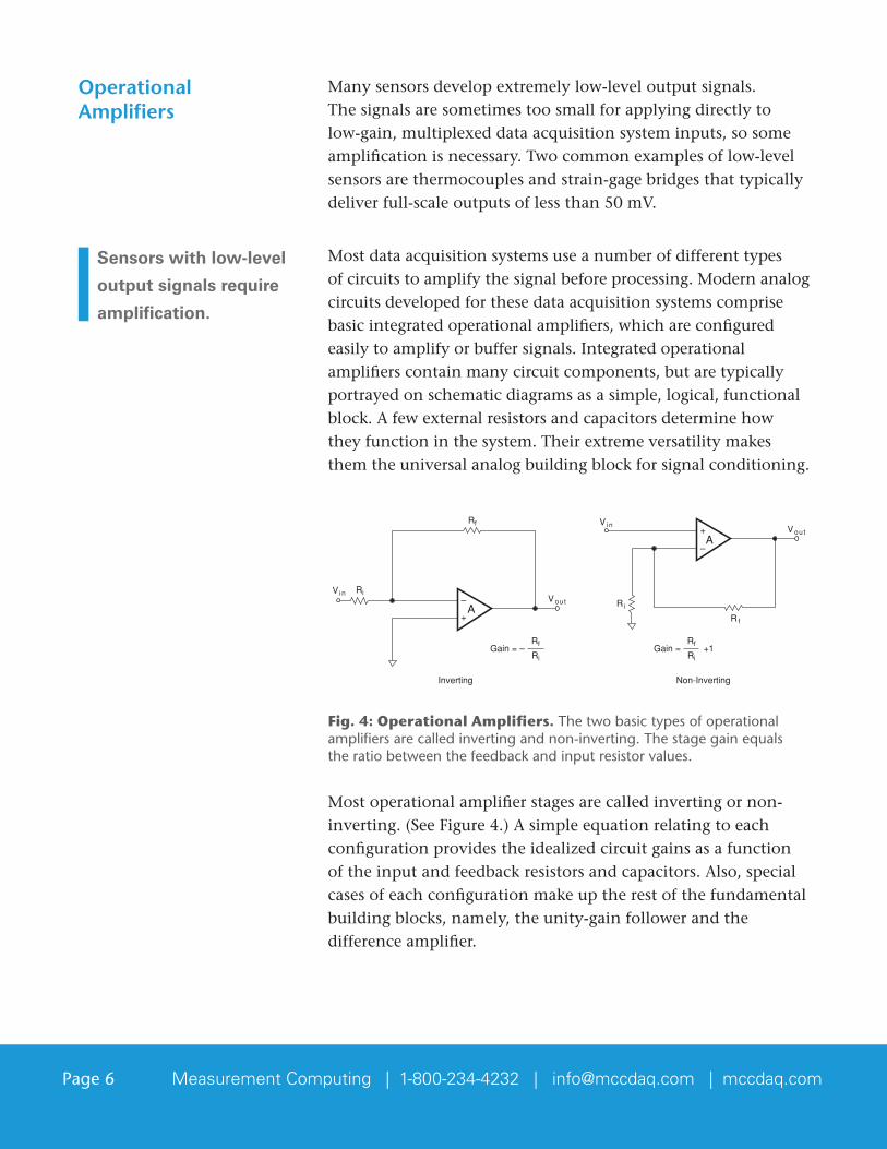
Most data acquisition systems use a number of different types of circuits to amplify the signal before processing. Modern analog circuits developed for these data acquisition systems comprise basic integrated operational amplifiers, which are configured easily to amplify or buffer signals. Integrated operational amplifiers contain many circuit components, but are typically portrayed on schematic diagrams as a simple, logical, functional block.Afewexternalresistorsandcapacitorsdeterminehowthey function in the system. Their extreme versatility makes them the universal analog building block for signal conditioning.
Figure 5.04
+
–
Inverting Non-Inverting
Gain = –Rf
RiGain = +1
–
+
Rf
Ri
Ri
R f
Ri
Rf
A
A
Vin
V inVout
Vout
Fig. 4: Operational Amplifiers. The two basic types of operational amplifiers are called inverting and non-inverting. The stage gain equals the ratio between the feedback and input resistor values.
Most operational amplifier stages are called inverting or non-inverting.(SeeFigure4.)Asimpleequationrelatingtoeachconfiguration provides the idealized circuit gains as a function oftheinputandfeedbackresistorsandcapacitors.Also,specialcases of each configuration make up the rest of the fundamental building blocks, namely, the unity-gain follower and the difference amplifier.
Operational Amplifiers
Sensors with low-level
output signals require
amplification.
Page 7 Measurement Computing | 1-800-234-4232 | [email protected] | mccdaq.com
A–
+
Rf 100 kΩ
0 A
0 AIo
Ri 10 kΩ
IF = Ii
Vo = VRL
Ed = 0 VIi
V(–) = V(+) = 0 Vvirtual ground
+
–Vin = 0.5 V
Figure 5.05
RL
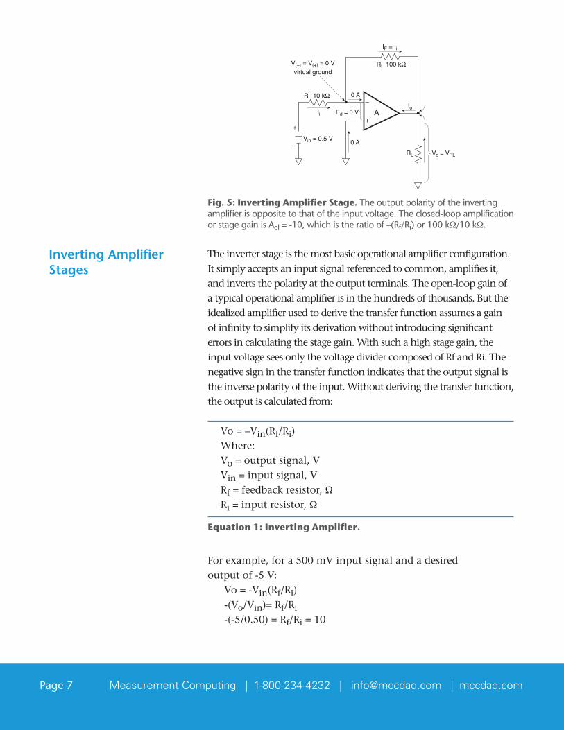
Fig. 5: Inverting Amplifier Stage. The output polarity of the inverting amplifier is opposite to that of the input voltage. The closed-loop amplification or stage gain is Acl = -10, which is the ratio of –(Rf/Ri) or 100 kΩ/10 kΩ.
The inverter stage is the most basic operational amplifier configuration. It simply accepts an input signal referenced to common, amplifies it, and inverts the polarity at the output terminals. The open-loop gain of a typical operational amplifier is in the hundreds of thousands. But the idealized amplifier used to derive the transfer function assumes a gain of infinity to simplify its derivation without introducing significant errors in calculating the stage gain. With such a high stage gain, the input voltage sees only the voltage divider composed of Rf and Ri. The negative sign in the transfer function indicates that the output signal is the inverse polarity of the input. Without deriving the transfer function, the output is calculated from:
Vo = –Vin(Rf/Ri)Where:Vo = output signal, VVin = input signal, VRf = feedback resistor, ΩRi = input resistor, Ω
Equation 1: Inverting Amplifier.
Forexample,fora500mVinputsignalandadesired output of -5 V: Vo = -Vin(Rf/Ri) -(Vo/Vin)= Rf/Ri -(-5/0.50) = Rf/Ri=10
Inverting Amplifier Stages

Page 8 Measurement Computing | 1-800-234-4232 | [email protected] | mccdaq.com
Therefore, the ratio between input and feedback resistors should be10,soRfmustbe100kΩwhenselectinga10kΩ resistor for Ri.(SeeFigure5.)
The maximum input signal that the amplifier can handle without damage is usually about 2 V less than the supply voltage.Forexample,whenthesupplyis±15VDC,theinputsignalshouldnotexceed±13VDC.Thisisthesinglemostcritical characteristic of the operational amplifier that limits its voltage handling ability.
A–
+
Rf 100 kΩ
Io
Ri 10 kΩ
IF = Ii
Vo = VRL
0 V
Ii
Vin = 0.5 V–
Vin
+
RL 10 kΩ
IL
Figure 5.06
Fig. 6: Non-Inverting Amplifier Stage. The input and output polarities of the non-inverting amplifier are the same. The gain of the stage is Acl = 11 or (Rf + Ri)/Ri.
The non-inverting amplifier is similar to the previous circuit, but thephaseoftheoutputsignalmatchestheinput.Also,thegainequation simply depends on the voltage divider composedofRfandRi.(SeeFigure6.)
Non-Inverting Amplifier Stages
Page 9 Measurement Computing | 1-800-234-4232 | [email protected] | mccdaq.com
The simplified transfer function is:
Vo = Vin(Rf+Ri)/Ri
Equation 2: Non-Inverting Amplifier.
Forthesame500mVinputsignal, Rf=100kΩ, and Ri=10kΩ: Vo/Vin = (Rf+Ri)/Ri, Vo = Vi(Rf+Ri)/Ri Vo=0.50(100k+10k)/10k Vo=0.50(110k/10k)=0.50(11) Vo = 5.5V
The input voltage limitations discussed for inverting amplifiers apply equally well to the non-inverting amplifier configuration.
A
–
+
Rf
Vo =g(V1 - V2)
+
–V1
Rf100 kΩ
+
–
Feedback gain resistor
V2
g =RfRi
Terminatingresistor
Figure 5.07
0.1% resistors
100 kΩ
100 kΩ
100 kΩ
Ri
Ri
RL
Optionalgroundconnection
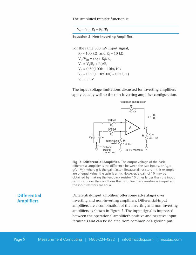
Fig. 7: Differential Amplifier. The output voltage of the basic differential amplifier is the difference between the two inputs, or Acl = g(V1-V2), where g is the gain factor. Because all resistors in this example are of equal value, the gain is unity. However, a gain of 10 may be obtained by making the feedback resistor 10 times larger than the input resistors, under the conditions that both feedback resistors are equal and the input resistors are equal.
Differential-input amplifiers offer some advantages over inverting and non-inverting amplifiers. Differential-input amplifiers are a combination of the inverting and non-inverting amplifiersasshowninFigure7.Theinputsignalisimpressedbetween the operational amplifier’s positive and negative input terminals and can be isolated from common or a ground pin.
Differential Amplifiers
Page 10 Measurement Computing | 1-800-234-4232 | [email protected] | mccdaq.com
The optional ground pin is the key to the amplifier’s flexibility. The output signal of the differential-input amplifier responds only to the differential voltage that exists between the two input terminals. The transfer function for this amplifier is:
Vo = (Rf/Ri)(V1 – V2)
Equation 3: Differential Amplifier.
Foraninputsignalof50mVwhere: V1=1.050VandV2=1.000V Vo = (Rf/Ri)(V1 – V2) Vo=(100k/100k)(0.05V) Vo = 0.05 V
Foragainof10whereRf=100kandRi=10k: Vo = (Rf/Ri)(V1 – V2) Vo=(100k/10k)(0.05V) Vo = 0.50V
The major benefit of the differential amplifier is its ability to reject voltages that are common to both inputs while amplifying the difference voltage. The voltages that are common to both inputs are called common-mode voltages (Vcm or CMV). The CMV rejection quality can be demonstrated by connecting the two inputs together and to a voltage source referenced toground.Althoughavoltageispresentatbothinputs,thedifferential amplifier responds only to the difference, which in this case is zero. The ideal operational amplifier yields zero output volts under this arrangement. (Refer to Instrumentation Amplifiers[page11]andHighCommon-ModeAmplifiers[page13]formoreinformation.)
Page 11 Measurement Computing | 1-800-234-4232 | [email protected] | mccdaq.com
A–
+
A0
Vi
Iin(–) = 0 A
4 kΩ
2 kΩ
1 kΩ
1 kΩ
+5 V
0
1
0A1
A2
R’F
R’i
S7
S3
S2
S1
S0 G=1
G=2
G=4
G=8
Three 1 kΩpull-up
resistors
TTL logic level,010, closes S2
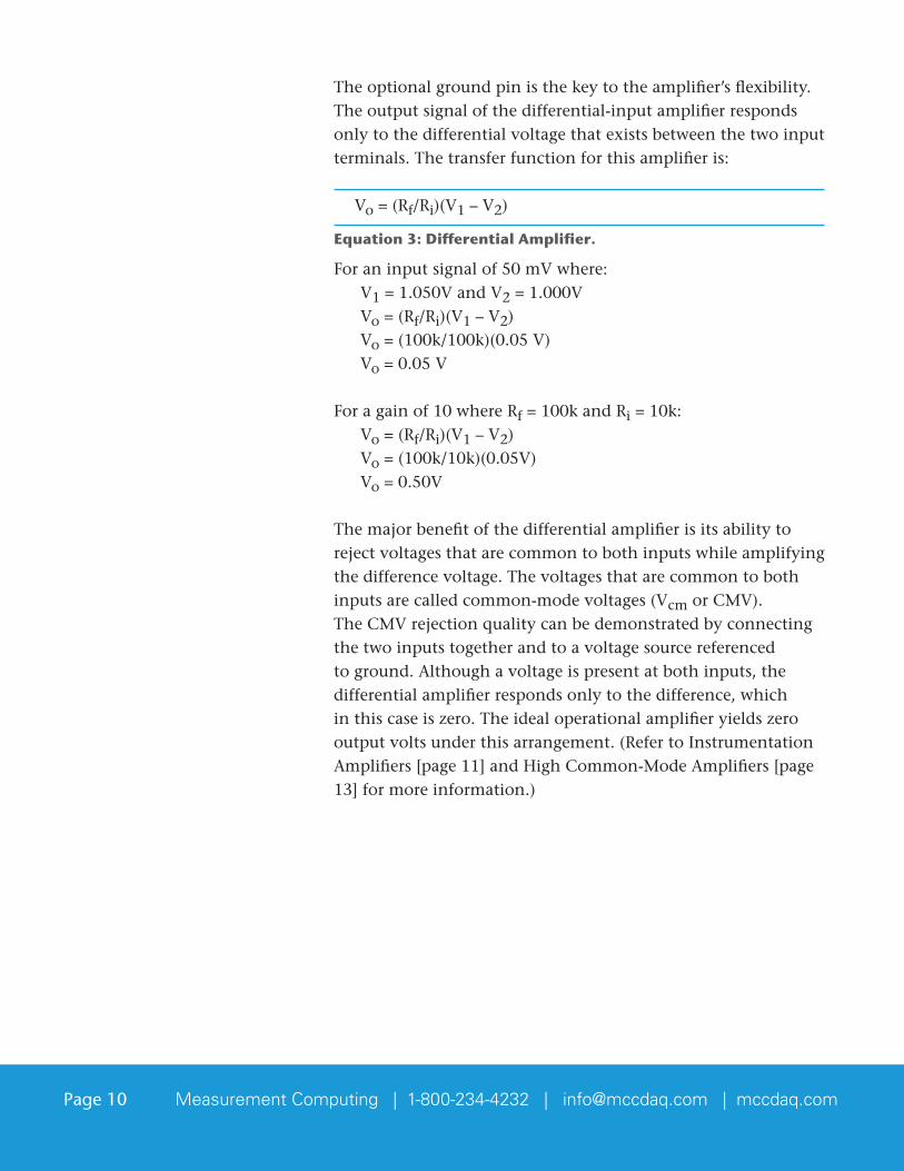
Figure 5.08 Fig. 8: Programmable Gain Amplifier. The non-inverting amplifier is configured for programmable gain and controlled by the binary input signals from a microprocessor to the addressable inputs of the analog switch.
Programmable gain amplifiers are typically non-inverting operational amplifiers with a digitally controlled analog switchconnectedtoseveralresistorsinitsfeedbackloop.Anexternal computer or another logic or binary signal controls the addressable inputs of the analog switch so it selects a certain resistorforparticulargain.(SeeFigure8.)Theinputsignalthencan be measured and displayed without distortion.
Instrumentation Amplifiers
Because signal levels from some transducers may be just a few microvolts, ground loop and spurious interference problems frequently arise when amplifying them. Other transducers provide output signals from differential signal sources to minimize grounding problems and reduce the effect of common-modeinterferingsignals.Amplifiersusedintheseapplications must have the following characteristics:
Programmable Gain Amplifiers
A Fundamental Problem
Page 12 Measurement Computing | 1-800-234-4232 | [email protected] | mccdaq.com
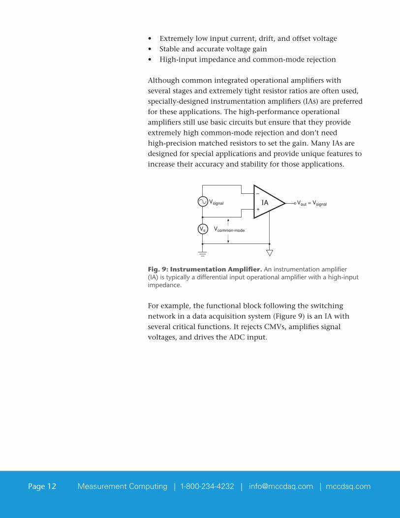
• Extremelylowinputcurrent,drift,andoffsetvoltage• Stableandaccuratevoltagegain• High-inputimpedanceandcommon-moderejection
Althoughcommonintegratedoperationalamplifierswithseveral stages and extremely tight resistor ratios are often used, specially-designedinstrumentationamplifiers(IAs)arepreferredfor these applications. The high-performance operational amplifiers still use basic circuits but ensure that they provide extremely high common-mode rejection and don’t need high-precisionmatchedresistorstosetthegain.ManyIAsaredesigned for special applications and provide unique features to increase their accuracy and stability for those applications.
Vout = Vsignal
–
+
Vcommon-modeVs
Vsignal
Figure 5.09
IA
Fig. 9: Instrumentation Amplifier. An instrumentation amplifier (IA) is typically a differential input operational amplifier with a high-input impedance.
Forexample,thefunctionalblockfollowingtheswitchingnetworkinadataacquisitionsystem(Figure9)isanIAwithseveral critical functions. It rejects CMVs, amplifies signal voltages,anddrivestheADCinput.
Page 13 Measurement Computing | 1-800-234-4232 | [email protected] | mccdaq.com
A
–
+
VoCM ≈ 0
95.3 kΩ
Common-modeadjustment
+
–VCM
Rf
Figure 5.10
100 kΩ
100 kΩ
100 kΩ
0.1% resistors
Rf
Ri
RiRL
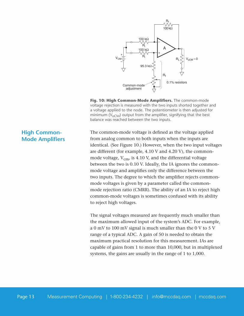
Fig. 10: High Common-Mode Amplifiers. The common-mode voltage rejection is measured with the two inputs shorted together and a voltage applied to the node. The potentiometer is then adjusted for minimum (VoCM) output from the amplifier, signifying that the best balance was reached between the two inputs.
The common-mode voltage is defined as the voltage applied from analog common to both inputs when the inputs are identical.(SeeFigure10.)However,whenthetwoinputvoltagesaredifferent(forexample,4.10Vand4.20V),thecommon-mode voltage, Vcm,is4.10V,andthedifferentialvoltagebetweenthetwois0.10V.Ideally,theIAignoresthecommon-mode voltage and amplifies only the difference between the two inputs. The degree to which the amplifier rejects common-mode voltages is given by a parameter called the common-moderejectionratio(CMRR).TheabilityofanIAtorejecthighcommon-mode voltages is sometimes confused with its ability to reject high voltages.
The signal voltages measured are frequently much smaller than themaximumallowedinputofthesystem’sADC.Forexample,a0mVto100mVsignalismuchsmallerthanthe0Vto5VrangeofatypicalADC.Againof50isneededtoobtainthemaximumpracticalresolutionforthismeasurement.IAsarecapableofgainsfrom1tomorethan10,000,butinmultiplexedsystems,thegainsareusuallyintherangeof1to1,000.
High Common-Mode Amplifiers
Page 14 Measurement Computing | 1-800-234-4232 | [email protected] | mccdaq.com
Measurement errors come from the non-ideal ON resistance of analog switches added to the impedance of any signal source. Buttheextremelyhigh-inputimpedanceoftheIAminimizesthiseffect.TheinputstageofanIAconsistsoftwovoltagefollowers, which have the highest input impedance of any common amplifier configuration. The high impedance and extremely low bias current drawn from the input signal generate a minimal voltage drop across the analog switch sections and produceamoreaccuratesignalfortheIAinput.
TheIAhaslowoutputimpedance,whichisidealfordriving theADCinput.ThetypicalADCdoesnothavehighorconstantinput impedance, so the preceding stage must provide a signal with the lowest impedance practical.
SomeIAsarelimitedbyoffsetvoltage,gainerror,limitedbandwidth, and settling time. The offset voltage and gain error can be calibrated out as part of the measurement, but the bandwidth and settling time limit the frequencies of amplified signals and the frequency at which the input switching system canswitchchannelsbetweensignals.AseriesofsteadyDCvoltagesappliedtoanIAinrapidsuccessiongeneratesadifficultcomposite signal to amplify. The settling time of the amplifier is the time necessary for the output to reach final amplitude to withinsomesmallerror(often0.01%)afterthesignalisappliedtotheinput.Inasystemthatscansinputsat100kHz,thetotaltimespentreadingeachchannelis10μs.Ifanalog-to-digitalconversionrequires8μs,settlingtimeoftheinputsignalto therequiredaccuracymustbelessthan2μs.
Althoughcalibratingasystemcanminimizeoffsetvoltageandgainerror,calibrationisnotalwaysneeded.Forexample,an amplifier with an offset voltage of 0.5 mV and a gain of 2 measuringa2Vsignaldevelopsanerrorofonly1mVin4Vontheoutput,or0.025%.Bycomparison,anoffsetof0.5mVandagainof50measuringa100mVsignaldevelopanerrorof25mVin5Vor0.5%.Gainerrorissimilar.Astagegainerrorof0.25%hasagreateroveralleffectasgainincreases,producinglarger absolute errors at higher gains and minimal errors at unity gain. System software can generally handle known
The typical ADC does not
have high or constant
input impedance, so the
preceding stage must
provide a signal with
the lowest impedance
practical.
Page 15 Measurement Computing | 1-800-234-4232 | [email protected] | mccdaq.com
calibrationconstantswithmx+bcalibrationroutines,butsomemeasurements are not critical enough to justify the effort.
A1
–
+
V1
Ri1
V’o
0V
–
+
Input 1
A2
–
+
R
RRm
V2
–
+
Input 20V
A3
–
+Vo
Reference
Sense
Buffered inputstage
Differential amplifier outputstage
Figure 5.11
Rin–∞Ω~
Rin–∞Ω~
Rf1
Ri2Rf2
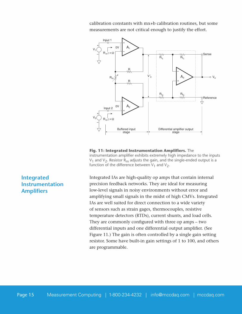
Fig. 11: Integrated Instrumentation Amplifiers. The instrumentation amplifier exhibits extremely high impedance to the inputs V1 and V2. Resistor Rm adjusts the gain, and the single-ended output is a function of the difference between V1 and V2.
IntegratedIAsarehigh-qualityopampsthatcontaininternalprecision feedback networks. They are ideal for measuring low-level signals in noisy environments without error and amplifying small signals in the midst of high CMVs. Integrated IAsarewellsuitedfordirectconnectiontoawidevarietyof sensors such as strain gages, thermocouples, resistive temperature detectors (RTDs), current shunts, and load cells. They are commonly configured with three op amps – two differential inputs and one differential output amplifier. (See Figure11.)Thegainisoftencontrolledbyasinglegainsettingresistor.Somehavebuilt-ingainsettingsof1to100,andothersare programmable.
Integrated Instrumentation Amplifiers
Page 16 Measurement Computing | 1-800-234-4232 | [email protected] | mccdaq.com
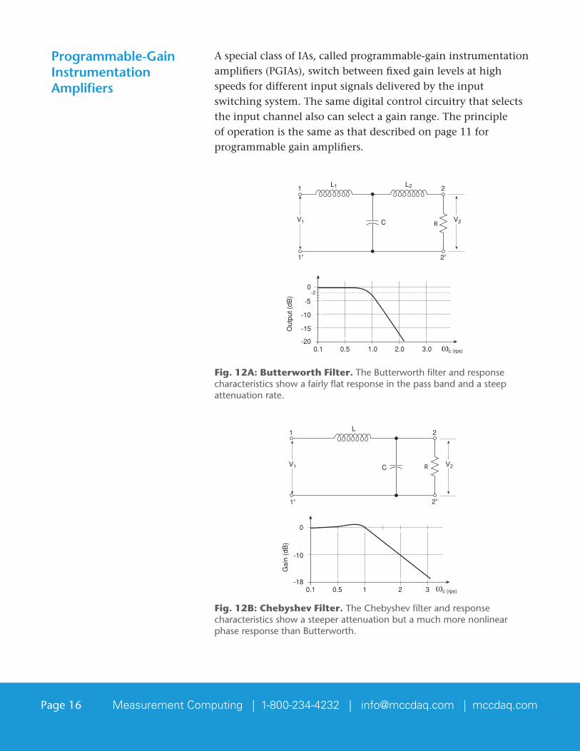
AspecialclassofIAs,calledprogrammable-gaininstrumentationamplifiers(PGIAs),switchbetweenfixedgainlevelsathighspeeds for different input signals delivered by the input switching system. The same digital control circuitry that selects the input channel also can select a gain range. The principle ofoperationisthesameasthatdescribedonpage11forprogrammable gain amplifiers.
L1
V1
L2
V2C
1’ 2’
R
1 2
Figure 5.12_A_pt1
0
ωc (rps)0.1-20
-2
0.5 1.0 2.0 3.0
Out
put (
dB)
-15
-10
-5
Figure 5.12_A_pt2
Wc (rps)
Fig. 12A: Butterworth Filter. The Butterworth filter and response characteristics show a fairly flat response in the pass band and a steep attenuation rate.
L
C
2’
1 2
Figure 5.12_B_pt1
RV1 V2
1’
0
ωc (rps)0.1-18
0.5 1 2 3
Gai
n (d
B)
-10
5.12_B_pt2.eps
Fig. 12B: Chebyshev Filter. The Chebyshev filter and response characteristics show a steeper attenuation but a much more nonlinear phase response than Butterworth.
Programmable-Gain Instrumentation Amplifiers
Page 17 Measurement Computing | 1-800-234-4232 | [email protected] | mccdaq.com
Odd order N
RL
1
Figure 5.12_C_pt1
L1
C1
Rs
C2 CN
LN
RL
V1
Even order N
0
ω(rps)1k
-100
10k
Gai
n (d
B)
-10
Figure 5.12_C_pt2
-50
-140100k
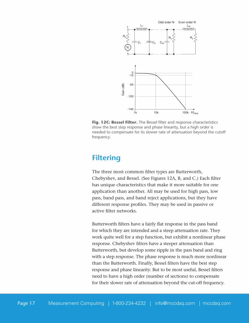
Fig. 12C: Bessel Filter. The Bessel filter and response characteristics show the best step response and phase linearity, but a high order is needed to compensate for its slower rate of attenuation beyond the cutoff frequency.
Filtering
The three most common filter types are Butterworth, Chebyshev,andBessel.(SeeFigures12A,B,andC.)Eachfilterhas unique characteristics that make it more suitable for one applicationthananother.Allmaybeusedforhighpass,lowpass, band pass, and band reject applications, but they have different response profiles. They may be used in passive or active filter networks.
Butterworth filters have a fairly flat response in the pass band for which they are intended and a steep attenuation rate. They work quite well for a step function, but exhibit a nonlinear phase response. Chebyshev filters have a steeper attenuation than Butterworth, but develop some ripple in the pass band and ring with a step response. The phase response is much more nonlinear thantheButterworth.Finally,Besselfiltershavethebeststepresponse and phase linearity. But to be most useful, Bessel filters need to have a high order (number of sections) to compensate for their slower rate of attenuation beyond the cut-off frequency.
Page 18 Measurement Computing | 1-800-234-4232 | [email protected] | mccdaq.com
Figure 5.13 B
–
+R
C
To MuxA
Vin
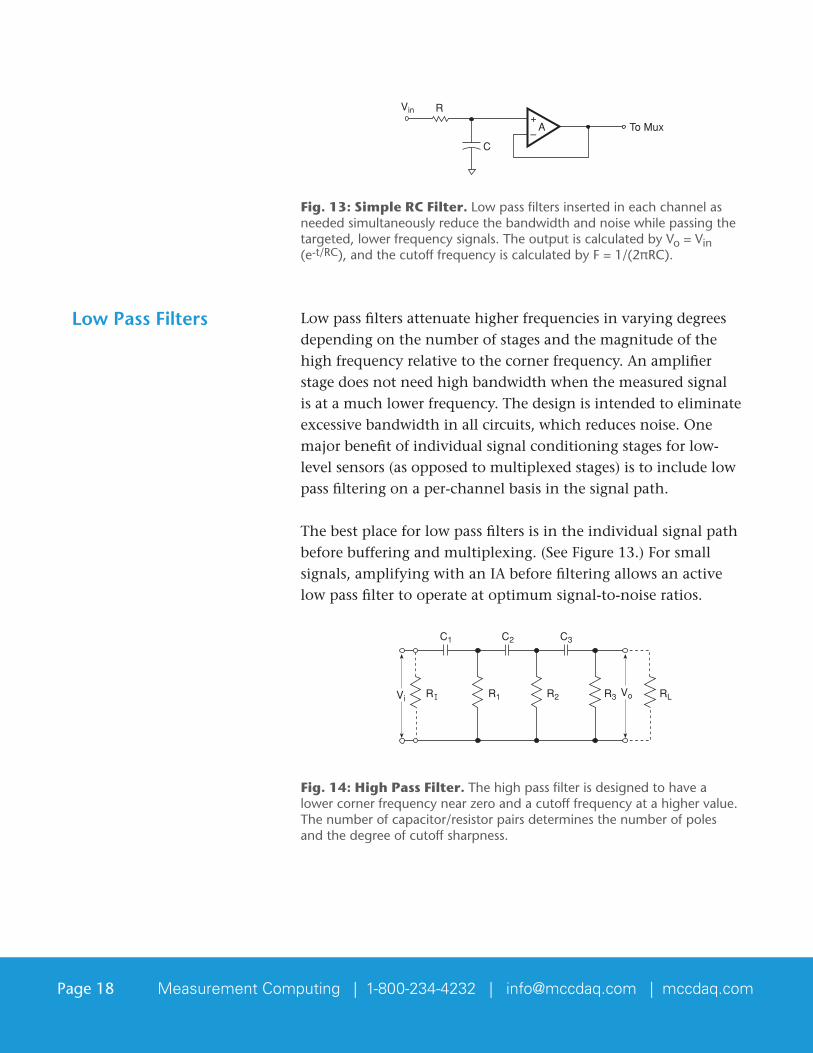
Fig. 13: Simple RC Filter. Low pass filters inserted in each channel as needed simultaneously reduce the bandwidth and noise while passing the targeted, lower frequency signals. The output is calculated by Vo = Vin (e-t/RC), and the cutoff frequency is calculated by F = 1/(2πRC).
Lowpassfiltersattenuatehigherfrequenciesinvaryingdegreesdepending on the number of stages and the magnitude of the highfrequencyrelativetothecornerfrequency.Anamplifierstage does not need high bandwidth when the measured signal is at a much lower frequency. The design is intended to eliminate excessive bandwidth in all circuits, which reduces noise. One major benefit of individual signal conditioning stages for low-level sensors (as opposed to multiplexed stages) is to include low pass filtering on a per-channel basis in the signal path.
The best place for low pass filters is in the individual signal path beforebufferingandmultiplexing.(SeeFigure13.)Forsmallsignals,amplifyingwithanIAbeforefilteringallowsanactivelow pass filter to operate at optimum signal-to-noise ratios.
Figure 5.14
RI R1 R2 R3 RL
C1 C2 C3
ViVo
Fig. 14: High Pass Filter. The high pass filter is designed to have a lower corner frequency near zero and a cutoff frequency at a higher value. The number of capacitor/resistor pairs determines the number of poles and the degree of cutoff sharpness.
Low Pass Filters
Page 19 Measurement Computing | 1-800-234-4232 | [email protected] | mccdaq.com
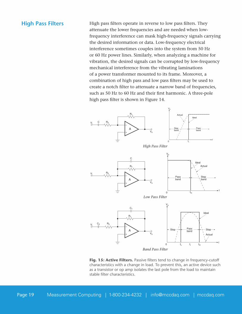
High pass filters operate in reverse to low pass filters. They attenuate the lower frequencies and are needed when low-frequency interference can mask high-frequency signals carrying thedesiredinformationordata.Low-frequencyelectricalinterference sometimes couples into the system from 50 Hz or60Hzpowerlines.Similarly,whenanalyzingamachineforvibration, the desired signals can be corrupted by low-frequency mechanical interference from the vibrating laminations of a power transformer mounted to its frame. Moreover, a combination of high pass and low pass filters may be used to create a notch filter to attenuate a narrow band of frequencies, suchas50Hzto60Hzandtheirfirstharmonic.Athree-polehighpassfilterisshowninFigure14.
Figure 5.15_A
–
+
Vi
Vo
C R2
R1
A
fL
Figure 5.15_B
0
Vo
f
Stopband
Passband
IdealActual
High Pass Filter
Figure 5.15 C
–
+
Vi
Vo
C
R2
R1
A
fH
Figure 5.15_D
0
Vo
f
Stopband
Passband
IdealActual
Low Pass Filter
Figure 5.15 E
–
+
Vi
Vo
C2 R2
R1
C1
A
fL
Figure 5.15_F
0
Vo
f
Stop Passband
Ideal
Actual
Stop
fr fH
Band Pass Filter
Fig. 15: Active Filters. Passive filters tend to change in frequency-cutoff characteristics with a change in load. To prevent this, an active device such as a transistor or op amp isolates the last pole from the load to maintain stable filter characteristics.
High Pass Filters
Page 20 Measurement Computing | 1-800-234-4232 | [email protected] | mccdaq.com
Passive filters comprise discrete capacitors, inductors, and resistors.Asthefrequenciespropagatethroughthesenetworks,two problems arise: the desired signal is attenuated by a relatively small amount, and when connected to a load, the originalfilteringcharacteristicschange.Activefilters,ontheotherhand,avoidtheseproblems.(SeeFigure15.)Theycomprise operational amplifiers built with both discrete and integrated resistors, capacitors, and inductors. They can provide the proper pass band (or stop band) capability without loading the circuit, attenuating the desired signals, or changing the original filtering characteristics.
Althoughactivefiltersbuiltaroundoperationalamplifiersaresuperior to passive filters, they still contain both integrated and discrete resistors. Integrated-circuit resistors occupy a large space on the substrate, and their values can’t easily be made to withstand high tolerances, either in relative or absolute values. But capacitors with virtually identical values can be formed on integrated circuits more easily, and when used in a switching mode, they can replace the resistors in filters.
The switched-capacitor filter is a relatively recent improvement over the traditional filter. James Clerk Maxwell compared a switchedcapacitortoaresistorinatreatisein1892,butonlyrecently has the idea taken hold in a zero-offset electronic switch and a high-input impedance amplifier. The switched-capacitor concept is now used in extremely complex and accurate analog filter circuits.
Figure 5.16
V1V2
S2 S1
CC2 CC1
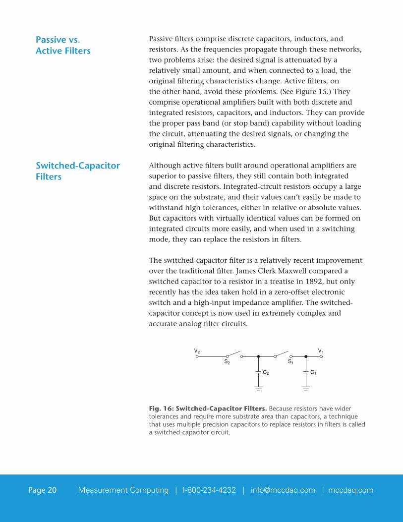
Fig. 16: Switched-Capacitor Filters. Because resistors have wider tolerances and require more substrate area than capacitors, a technique that uses multiple precision capacitors to replace resistors in filters is called a switched-capacitor circuit.
Passive vs. Active Filters
Switched-Capacitor Filters
Page 21 Measurement Computing | 1-800-234-4232 | [email protected] | mccdaq.com
The theory of operation of an RC equivalent switched filter isdepictedinFigure16.WithS2 closed and S1 open, a charge from V2 accumulates on C. Then, when S2 opens, S1 closes, and the capacitor transfers the charge to V1. This process repeats at a particular frequency, and the charge becomes a current by definition, that is, current equals the transfer of charge per unit time.
The derivation of the equation is beyond the scope of this discussion, but it can be shown that the equivalent resistor may be determined by:
(V2 – V1)/i=1/(fC) = RWhere:V2 = voltage source 2, VV1=voltagesource1,Vi=equivalentcurrent,Af = clock frequency, HzC=capacitor,FR = equivalent resistor, Ω
Equation 4: Switched-Capacitor Filters.
Equation 4 states that the switched capacitor is identical to a resistor within the constraints of the clock frequency and fixed capacitors. Moreover, the equivalent resistor’s effective value is inversely proportional to the frequency or the size of the capacitor.
100 kΩ
900 kΩ
RL
Figure 5.17
R2
R1
Vin
Vout
com.com.
ZL = Mux input
ZS = Source
ZS1 Meg 10 kΩ ZL90 kΩ 1 kΩ
9 kΩ
1 kΩ
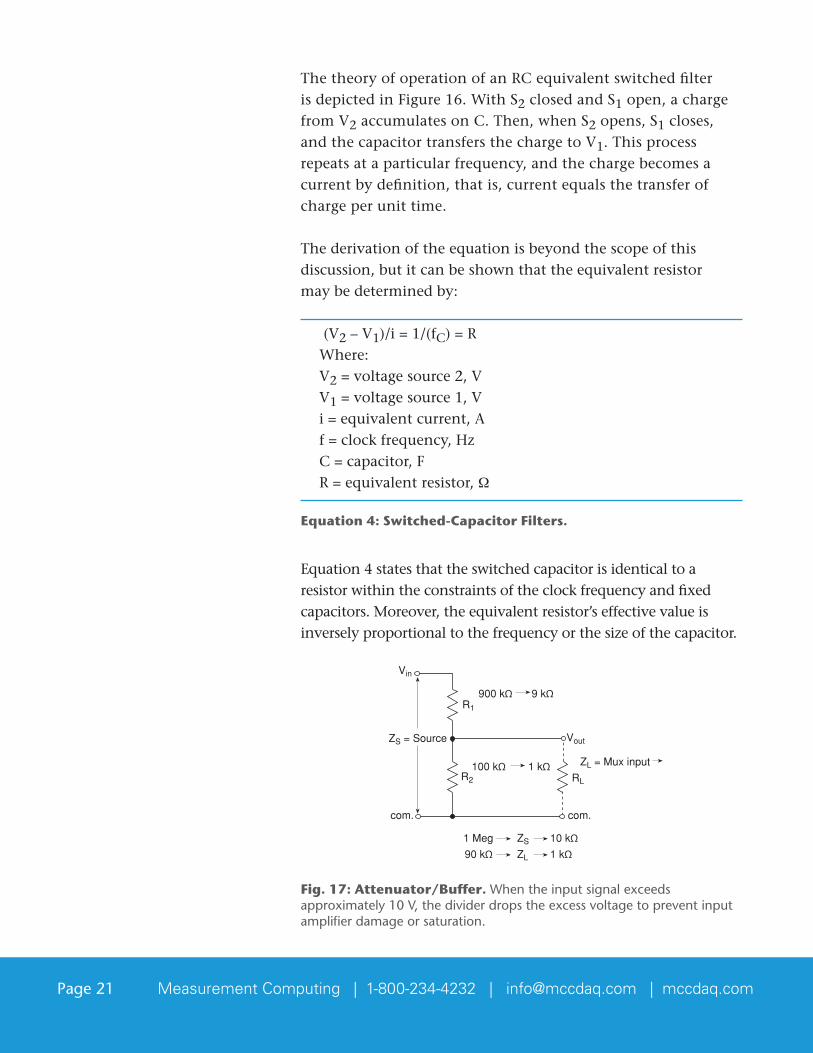
Fig. 17: Attenuator/Buffer. When the input signal exceeds approximately 10 V, the divider drops the excess voltage to prevent input amplifier damage or saturation.
Page 22 Measurement Computing | 1-800-234-4232 | [email protected] | mccdaq.com
Attenuation
Most data acquisition system inputs can measure voltages onlywithinarangeof5Vto10V.Highervoltagesmustbe attenuated. Straightforward resistive dividers can easily attenuateanyrangeofvoltages(seeFigure17),buttwodrawbackscomplicatethissimplesolution.First,voltagedividers present substantially lower impedances to the source than do direct analog inputs. Second, their output impedance ismuchtoohighformultiplexerinputs.Forexample,considera10:1dividerreading50V.Ifa900kΩanda100kΩ resistor arechosentoprovidea1MΩ load to the source, the impedance seenbytheanalogmultiplexerinputisabout90kΩ – still too high for an accurate multiplexed reading. When the valuesarebothreducedbyafactorof100–makingtheinputimpedancelessthan1kΩ – the input impedance seen by the measuredsourceis10kΩ, or 2 kΩ/V, which most instruments cannot tolerate in a voltage measurement. Therefore, simple attenuation is usually not practical with multiplexed inputs.
Figure 5.18 A
Vin
–
+ Vout
RL
RA
RB
Vout = RA + RB
RB Vin
A
Figure 5.18_B
RL
Vout
RE
+Vc
RB
Vin RA
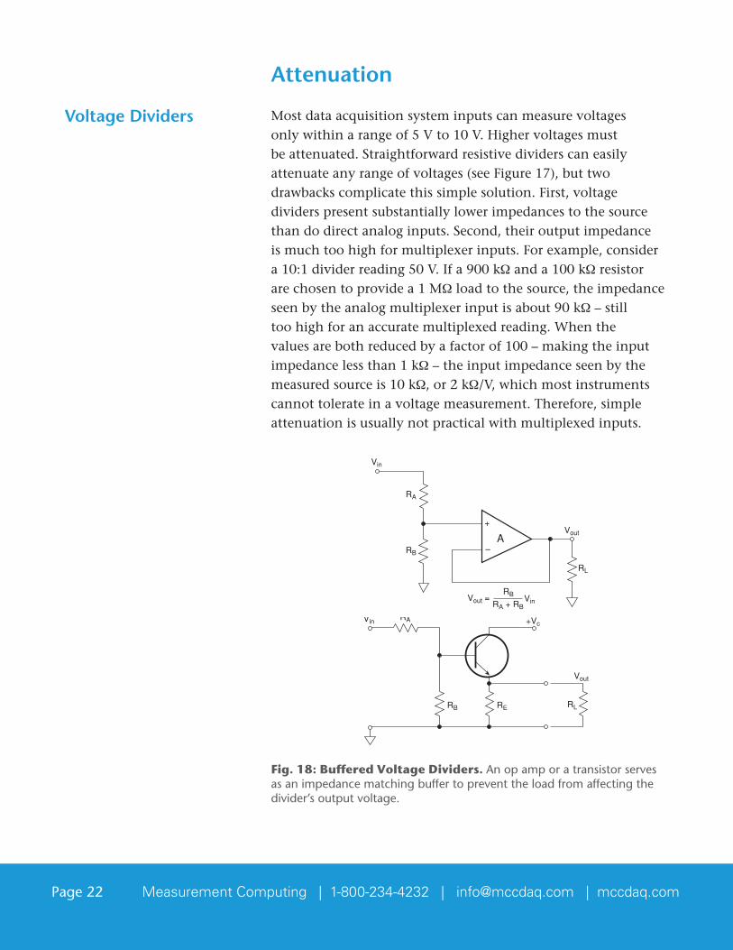
Fig. 18: Buffered Voltage Dividers. An op amp or a transistor serves as an impedance matching buffer to prevent the load from affecting the divider’s output voltage.
Voltage Dividers
Page 23 Measurement Computing | 1-800-234-4232 | [email protected] | mccdaq.com
To overcome the low-impedance loading effect of simple voltage dividers, use unity-gain buffer amplifiers on divider outputs. Adedicatedunity-gainbufferhashigh-inputimpedanceinthe MΩ range and does not load down the source, as does the network in the previous example. Moreover, the buffers’ output impedance is extremely low, which is necessary for the multiplexedanaloginput.(SeeFigure18.)
+–
Hi
Lo
Input channel (typ. of 8)
2 M
249 K
249 K
249 K
249 K
2 M
2.49 M 10 V
50 V
100 V
100 V
50 V
10 V2.49 M
+–
+–
220 pF
220 pF
Figure 5.19
Compensationcapacitors
Select divider ratios
A
A
A
Out
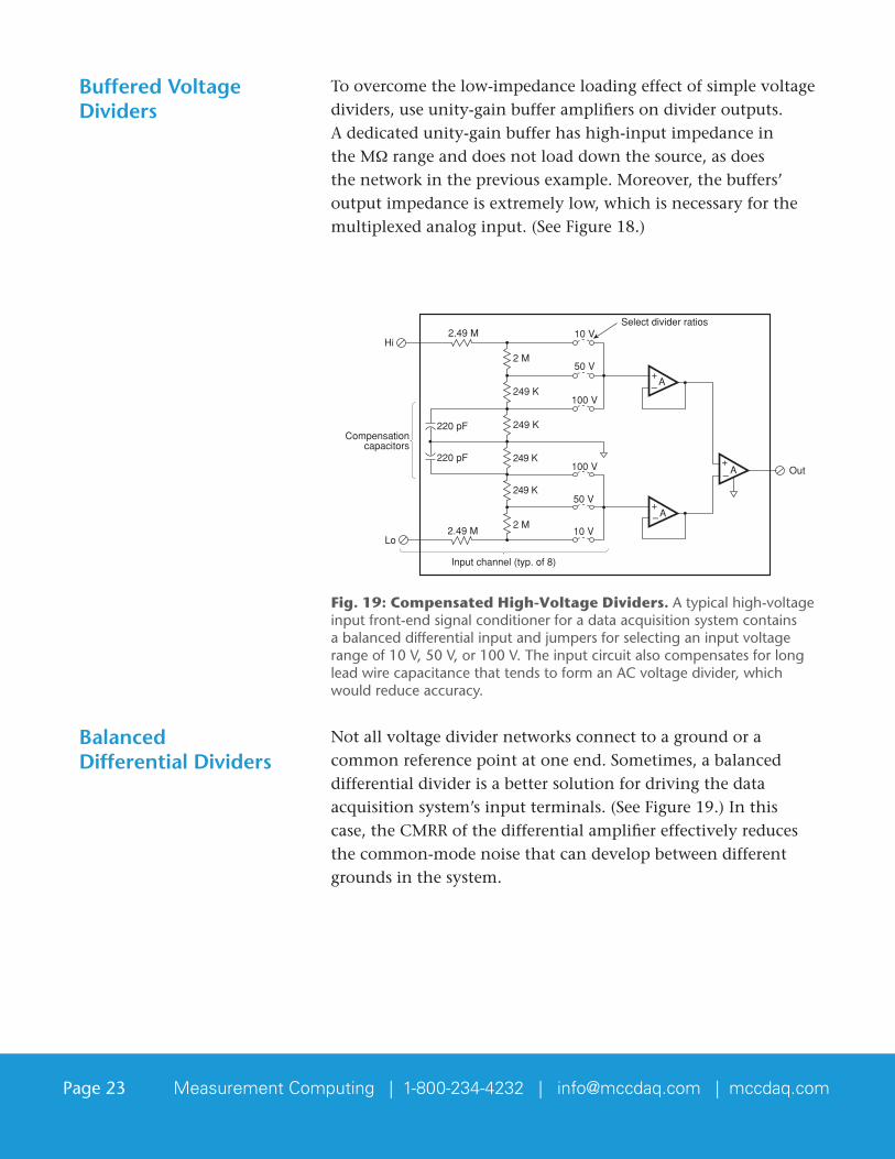
Fig. 19: Compensated High-Voltage Dividers. A typical high-voltage input front-end signal conditioner for a data acquisition system contains a balanced differential input and jumpers for selecting an input voltage range of 10 V, 50 V, or 100 V. The input circuit also compensates for long lead wire capacitance that tends to form an AC voltage divider, which would reduce accuracy.
Not all voltage divider networks connect to a ground or a common reference point at one end. Sometimes, a balanced differential divider is a better solution for driving the data acquisitionsystem’sinputterminals.(SeeFigure19.)Inthiscase, the CMRR of the differential amplifier effectively reduces the common-mode noise that can develop between different grounds in the system.
Buffered Voltage Dividers
Balanced Differential Dividers
Page 24 Measurement Computing | 1-800-234-4232 | [email protected] | mccdaq.com
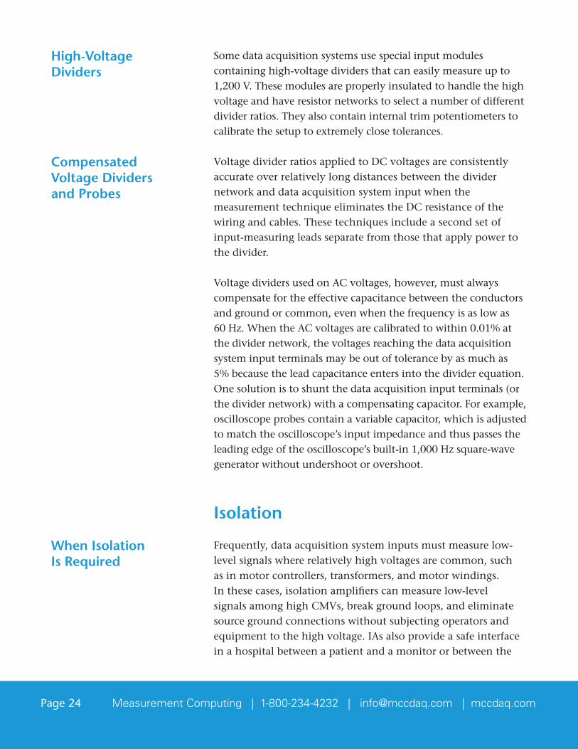
Some data acquisition systems use special input modules containing high-voltage dividers that can easily measure up to 1,200V.Thesemodulesareproperlyinsulatedtohandlethehighvoltage and have resistor networks to select a number of different divider ratios. They also contain internal trim potentiometers to calibrate the setup to extremely close tolerances.
Voltage divider ratios applied to DC voltages are consistently accurate over relatively long distances between the divider network and data acquisition system input when the measurement technique eliminates the DC resistance of the wiring and cables. These techniques include a second set of input-measuring leads separate from those that apply power to the divider.
VoltagedividersusedonACvoltages,however,mustalwayscompensate for the effective capacitance between the conductors and ground or common, even when the frequency is as low as 60Hz.WhentheACvoltagesarecalibratedtowithin0.01%atthe divider network, the voltages reaching the data acquisition system input terminals may be out of tolerance by as much as 5%becausetheleadcapacitanceentersintothedividerequation.One solution is to shunt the data acquisition input terminals (or thedividernetwork)withacompensatingcapacitor.Forexample,oscilloscope probes contain a variable capacitor, which is adjusted to match the oscilloscope’s input impedance and thus passes the leadingedgeoftheoscilloscope’sbuilt-in1,000Hzsquare-wavegenerator without undershoot or overshoot.
Isolation
Frequently,dataacquisitionsysteminputsmustmeasurelow-level signals where relatively high voltages are common, such as in motor controllers, transformers, and motor windings. In these cases, isolation amplifiers can measure low-level signals among high CMVs, break ground loops, and eliminate source ground connections without subjecting operators and equipmenttothehighvoltage.IAsalsoprovideasafeinterfacein a hospital between a patient and a monitor or between the
High-Voltage Dividers
Compensated Voltage Dividers and Probes
When Isolation Is Required
Page 25 Measurement Computing | 1-800-234-4232 | [email protected] | mccdaq.com
source and other electronic instruments and equipment. Other applications include precision bridge isolation amplifiers, photodiode amplifiers, multiple-port thermocouple and summingamplifiers,andisolated4mAto20mAcurrent-control loops.
Figure 5.20
+–
+
–
X X
S/HG=1
S/HG=6
C2
C2HC2L
C1
C1LC1H
Sense
Vin VoutSignalCom 2Signal
Com 2
ExtOsc
+V1 -V1Gnd1
Gnd2
+V2 -V2
Sense
C4
A1
Sense
A2
1pF
1pF
1pF
1pF
Isolation barrier
Input Output
R3
R4R2
C3R1 Ib
Ia
A A
Ib
Ia
R5
Adjustablegain stages
C5
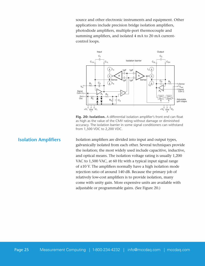
Fig. 20: Isolation. A differential isolation amplifier’s front end can float as high as the value of the CMV rating without damage or diminished accuracy. The isolation barrier in some signal conditioners can withstand from 1,500 VDC to 2,200 VDC.
Isolation amplifiers are divided into input and output types, galvanically isolated from each other. Several techniques provide the isolation; the most widely used include capacitive, inductive, andopticalmeans.Theisolationvoltageratingisusually1,200VACto1,500VAC,at60Hzwithatypicalinputsignalrangeof±10V.Theamplifiersnormallyhaveahighisolationmoderejectionratioofaround140dB.Becausetheprimaryjobofrelatively low-cost amplifiers is to provide isolation, many come with unity gain. More expensive units are available with adjustableorprogrammablegains.(SeeFigure20.)
Isolation Amplifiers
Page 26 Measurement Computing | 1-800-234-4232 | [email protected] | mccdaq.com
Figure 5.21
To ADCand
computer
VCC2
–
+
VCC2
+–
50 mV
Shunt
LoadVCC1
VCC1+ +
– –
200 VDC
Differentialisolationamplifier
G=1
200 VDCGroundisolation
Isolation barrier
Input Output
Highvoltage
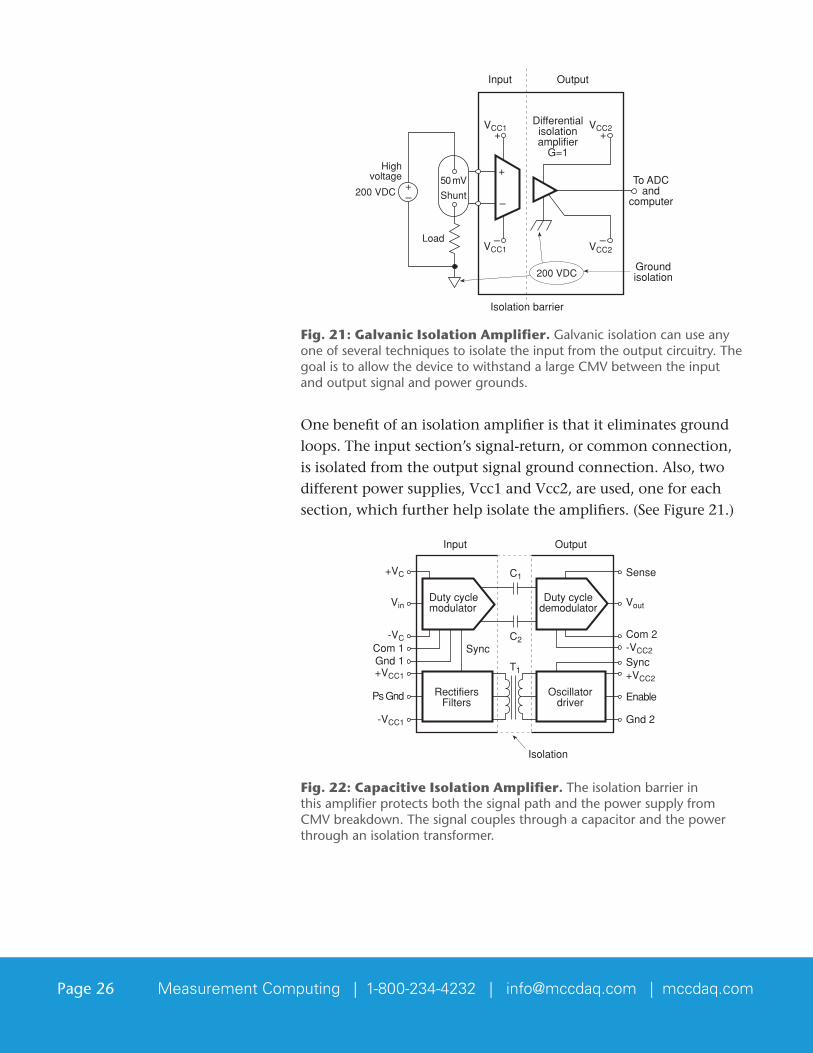
Fig. 21: Galvanic Isolation Amplifier. Galvanic isolation can use any one of several techniques to isolate the input from the output circuitry. The goal is to allow the device to withstand a large CMV between the input and output signal and power grounds.
One benefit of an isolation amplifier is that it eliminates ground loops. The input section’s signal-return, or common connection, isisolatedfromtheoutputsignalgroundconnection.Also,twodifferentpowersupplies,Vcc1andVcc2,areused,oneforeachsection,whichfurtherhelpisolatetheamplifiers.(SeeFigure21.)
Figure 5.22
Sense
Vin VoutDuty cyclemodulator
Duty cycledemodulator
RectifiersFilters
Oscillatordriver
Com 2-VCC2
Sync+VCC2
Enable
Gnd 2
+VC
+VCC1
-VCC1
Ps Gnd
-VCCom 1Gnd 1
Input
Sync
Output
Isolation
C1
C2
T1
Fig. 22: Capacitive Isolation Amplifier. The isolation barrier in this amplifier protects both the signal path and the power supply from CMV breakdown. The signal couples through a capacitor and the power through an isolation transformer.
Page 27 Measurement Computing | 1-800-234-4232 | [email protected] | mccdaq.com
Analogisolationamplifiersuseallthreetypesofisolationbetween input and output sections: capacitive, optical, and magnetic. One type of capacitively coupled amplifier modulates the input signal and couples it across a capacitive barrier with avaluedeterminedbythedutycycle.(SeeFigure22.)Theoutput section demodulates the signal, restores it to the original analog input equivalent, and filters the ripple component (a resultofthedemodulationprocess).Aftertheinputandoutputsections of the integrated circuit are fabricated, a laser trims both stages to precisely match their performance characteristics. The sections are then mounted on either end of the package, separatedbytheisolationcapacitors.Althoughtheschematicdiagram of the isolation amplifier looks quite simple, it can contain up to 250 or more integrated transistors.
Figure 5.23
+
–
Opticalcouplers
Vout
D2
Isolation
Vin
IREF2
OutputInput
IREF1
A+
–A
Vout = IinRf
+In
-In
+
–
Rin
Common 1 Common 2
D1
LED
Rf
I I
I
OutputInput
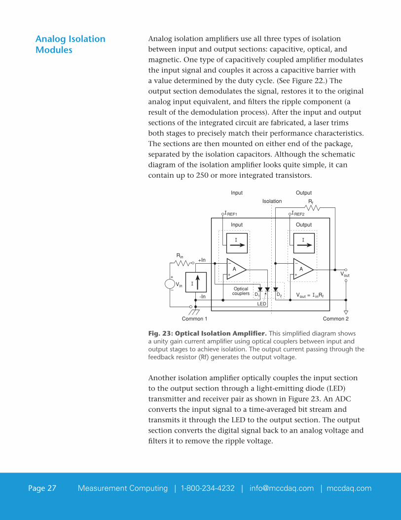
Fig. 23: Optical Isolation Amplifier. This simplified diagram shows a unity gain current amplifier using optical couplers between input and output stages to achieve isolation. The output current passing through the feedback resistor (Rf) generates the output voltage.
Anotherisolationamplifieropticallycouplestheinputsectiontotheoutputsectionthroughalight-emittingdiode(LED)transmitterandreceiverpairasshowninFigure23.AnADCconverts the input signal to a time-averaged bit stream and transmitsitthroughtheLEDtotheoutputsection.Theoutputsection converts the digital signal back to an analog voltage and filters it to remove the ripple voltage.
Analog Isolation Modules
Page 28 Measurement Computing | 1-800-234-4232 | [email protected] | mccdaq.com
Figure 5.24 A
A
Isolatedoutput
Vα
Signaltransmittedby magneticfield
Galvanicisolationby thin-filmdielectric
GMR resistors
IinHPlanar
coilA
OutputInput
Isolation
Vin
Vc
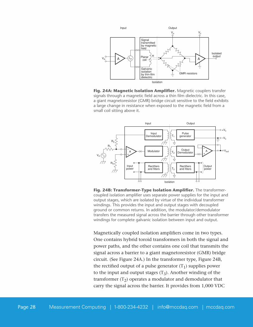
Fig. 24A: Magnetic Isolation Amplifier. Magnetic couplers transfer signals through a magnetic field across a thin film dielectric. In this case, a giant magnetoresistor (GMR) bridge circuit sensitive to the field exhibits a large change in resistance when exposed to the magnetic field from a small coil sitting above it.
Figure 5.24 B
InputDemodulator
Pulsegenerator
Modulator OutputDemodulator
Rectifiersand filters
Rectifiersand filters
+Vs
–Vs
+
–
+
–
Inputpower
Outputpower
A VoutA
Isolation
Vin
R1
R2
R3
T1
T2
T3
OutputInput
Fig. 24B: Transformer-Type Isolation Amplifier. The transformer-coupled isolation amplifier uses separate power supplies for the input and output stages, which are isolated by virtue of the individual transformer windings. This provides the input and output stages with decoupled ground or common returns. In addition, the modulator/demodulator transfers the measured signal across the barrier through other transformer windings for complete galvanic isolation between input and output.
Magnetically coupled isolation amplifiers come in two types. One contains hybrid toroid transformers in both the signal and power paths, and the other contains one coil that transmits the signalacrossabarriertoagiantmagnetoresistor(GMR)bridgecircuit.(SeeFigure24A.)Inthetransformertype,Figure24B,the rectified output of a pulse generator (T1) supplies power to the input and output stages (T3).Anotherwindingofthetransformer (T2) operates a modulator and demodulator that carrythesignalacrossthebarrier.Itprovidesfrom1,000VDC
Page 29 Measurement Computing | 1-800-234-4232 | [email protected] | mccdaq.com
to 3,500 VDC isolation among the amplifier’s three grounds, as well as an isolated output signal equal to the input signal with total galvanic isolation between input and output terminals.
Thesecondtype,theGMRamplifier,usesthesamebasictechnology as does high-speed hard disk drives. The coil generates a magnetic field with strength proportional to its inputdrivecurrentsignal,andthedielectricGMRamplifiesandconditionsit.Groundpotentialvariationsattheinputdonotgenerate current so they are not detected by the magnetoresistor structure.Asaresult,theoutputsignalequalstheinputsignalwith complete galvanic isolation. These units are relatively inexpensiveandcanwithstandfrom1,000VDCto3,500VDC.Full-powersignalfrequencyresponseislessthan2kHz,butsmall signal response is as much as 30 kHz.
Figure 5.25
Encode Decode
VDD2VDD1
Datain
Gnd Gnd
Dataout
Air coretransformer
Isolation
Input Output
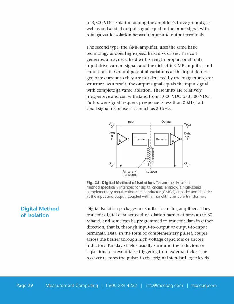
Fig. 25: Digital Method of Isolation. Yet another isolation method specifically intended for digital circuits employs a high-speed complementary metal–oxide–semiconductor (CMOS) encoder and decoder at the input and output, coupled with a monolithic air-core transformer.
Digital isolation packages are similar to analog amplifiers. They transmitdigitaldataacrosstheisolationbarrieratratesupto80Mbaud, and some can be programmed to transmit data in either direction, that is, through input-to-output or output-to-input terminals. Data, in the form of complementary pulses, couple across the barrier through high-voltage capacitors or aircore inductors.Faradayshieldsusuallysurroundtheinductorsorcapacitors to prevent false triggering from external fields. The receiver restores the pulses to the original standard logic levels.
Digital Method of Isolation
Page 30 Measurement Computing | 1-800-234-4232 | [email protected] | mccdaq.com
Aswithanalogamplifiers,thepowersuppliesforeachsectionarealsogalvanicallyisolated.(SeeFigure25.)
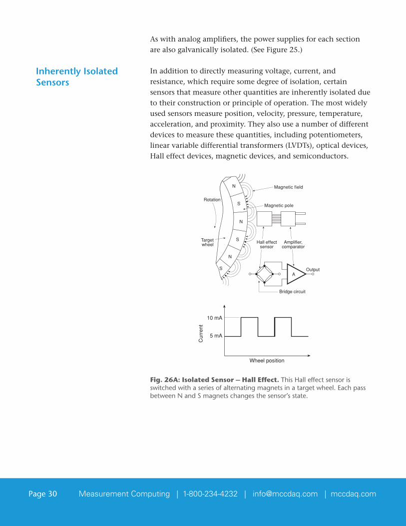
In addition to directly measuring voltage, current, and resistance, which require some degree of isolation, certain sensors that measure other quantities are inherently isolated due to their construction or principle of operation. The most widely used sensors measure position, velocity, pressure, temperature, acceleration, and proximity. They also use a number of different devices to measure these quantities, including potentiometers, linearvariabledifferentialtransformers(LVDTs),opticaldevices,Hall effect devices, magnetic devices, and semiconductors.
Hall effectsensor
Figure 5.26 A pt 1
Amplifier,comparator
N
N
N
S
S
S
AOutput
Rotation
Targetwheel
Bridge circuit
Magnetic pole
Magnetic field
Figure 5.26 A pt 2
5 mA
10 mA
Cur
rent
Wheel position
Fig. 26A: Isolated Sensor – Hall Effect. This Hall effect sensor is switched with a series of alternating magnets in a target wheel. Each pass between N and S magnets changes the sensor’s state.
Inherently Isolated Sensors
Page 31 Measurement Computing | 1-800-234-4232 | [email protected] | mccdaq.com
Figure 5.26 B
0
IL
IH
3 mV
-3 mV
t
Conditioned output
Input
Gap
Gap
Permanentmagnet
Hall effectsensor
Tonewheel
Vsens Iout
Rotation
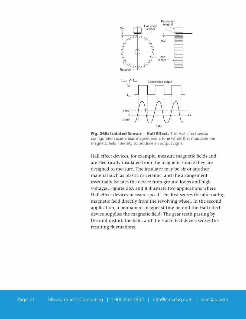
Fig. 26B: Isolated Sensor – Hall Effect. This Hall effect sensor configuration uses a bias magnet and a tone wheel that modulate the magnetic field intensity to produce an output signal.
Hall effect devices, for example, measure magnetic fields and are electrically insulated from the magnetic source they are designed to measure. The insulator may be air or another material such as plastic or ceramic, and the arrangement essentially isolates the device from ground loops and high voltages.Figures26AandBillustratetwoapplicationswhereHall effect devices measure speed. The first senses the alternating magnetic field directly from the revolving wheel. In the second application, a permanent magnet sitting behind the Hall effect device supplies the magnetic field. The gear teeth passing by the unit disturb the field, and the Hall effect device senses the resulting fluctuations.
Page 32 Measurement Computing | 1-800-234-4232 | [email protected] | mccdaq.com
220 VACpower
input
50 A to 100 Aload
Donut-shapedcurrent transformer
Ammeter
AC
Rs
To data acquisition system
To ammeter orshunt resistor, Rs
Figure 5.27 B,C,D
I
I
Common or return
I
I
Common or return
I
I
Common or return
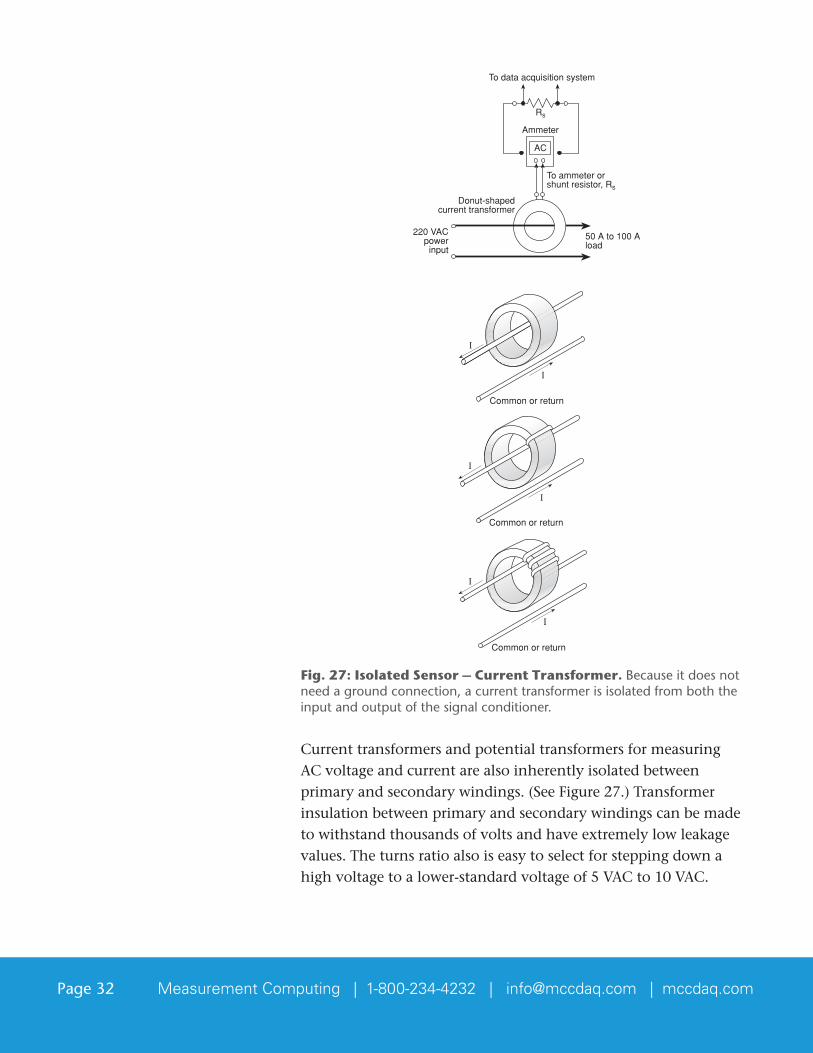
Fig. 27: Isolated Sensor – Current Transformer. Because it does not need a ground connection, a current transformer is isolated from both the input and output of the signal conditioner.
Current transformers and potential transformers for measuring ACvoltageandcurrentarealsoinherentlyisolatedbetweenprimaryandsecondarywindings.(SeeFigure27.)Transformerinsulation between primary and secondary windings can be made to withstand thousands of volts and have extremely low leakage values. The turns ratio also is easy to select for stepping down a highvoltagetoalower-standardvoltageof5VACto10VAC.
Page 33 Measurement Computing | 1-800-234-4232 | [email protected] | mccdaq.com
Figure 5.28 A
Variablereluctance
wheel speedsensor
Gearwheel
AC inputfrom sensor
DCreference
AC inputfrom sensor
Antilock brakecontroller
Figure 5.28 B
15 mA
5 mA
1.70V
1.0V
Digital output signal
Figure 5.28 C
Target
Signalprocessing
Wire coil Magnet
VR transducer
Digitaloutput
Analog in
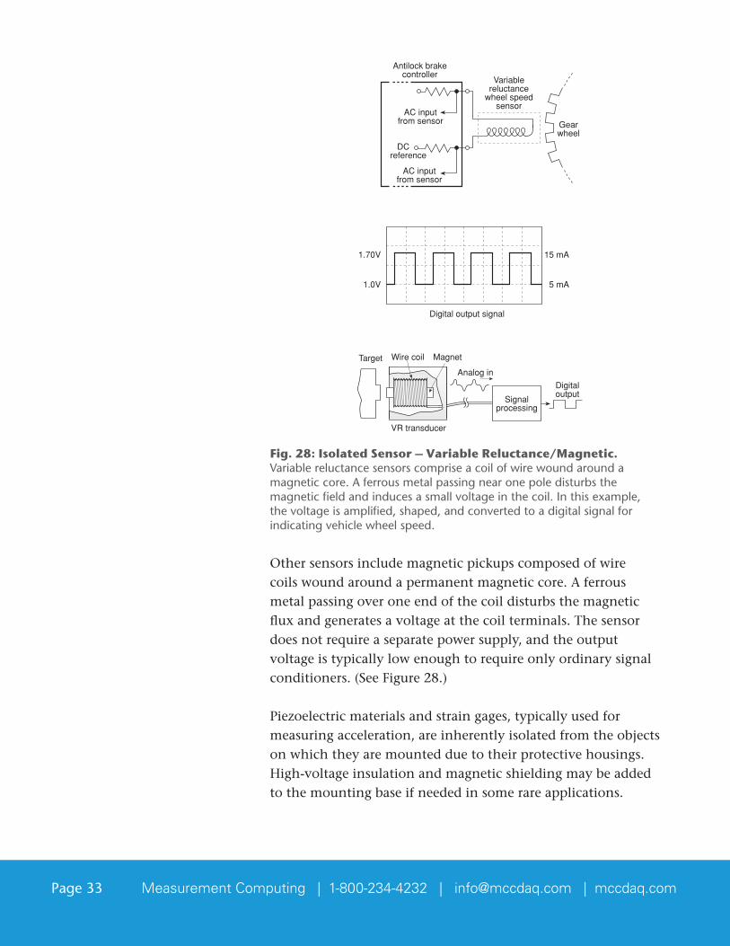
Fig. 28: Isolated Sensor – Variable Reluctance/Magnetic. Variable reluctance sensors comprise a coil of wire wound around a magnetic core. A ferrous metal passing near one pole disturbs the magnetic field and induces a small voltage in the coil. In this example, the voltage is amplified, shaped, and converted to a digital signal for indicating vehicle wheel speed.
Other sensors include magnetic pickups composed of wire coilswoundaroundapermanentmagneticcore.Aferrousmetal passing over one end of the coil disturbs the magnetic flux and generates a voltage at the coil terminals. The sensor does not require a separate power supply, and the output voltage is typically low enough to require only ordinary signal conditioners.(SeeFigure28.)
Piezoelectric materials and strain gages, typically used for measuring acceleration, are inherently isolated from the objects on which they are mounted due to their protective housings. High-voltage insulation and magnetic shielding may be added to the mounting base if needed in some rare applications.
Page 34 Measurement Computing | 1-800-234-4232 | [email protected] | mccdaq.com
LVDTscontainamodulatoranddemodulator(eitherinternallyor externally), require some small DC power, and provide a smallACorDCsignaltothedataacquisitionsystem.Often,theyarescaledtooutput0Vto5V.LVDTscanmeasurebothposition and acceleration.
Optical devices such as encoders are widely used in linear and rotarypositionsensors.Althoughtheyhavemanypossibleconfigurations, the basic principle of operation is based on the interruption of a light beam between an optical transmitter and receiver.Arevolvingopaquediscwithmultipleaperturesplacedbetween the transmitter and receiver alternately lets light through togeneratepulses.Usually,LEDsgeneratethelight,andaphotodiode on the opposite side detects the resulting pulses, which are then counted. The pulses can indicate position or velocity.
Linearization
The transfer function that relates the input to output for many electronic devices contains a nonlinear factor. This factor is usually small enough to ignore; however, in some applications, it must be compensated either in hardware or software.
60
2500˚500˚ 1000˚ 1500˚ 2000˚
Mill
ivol
ts
80
20
40
Figure 5.29
0
Temperature ˚C
K
J
E
RS
T
TYPE METALS+ –
E Chromel vs. ConstantanJ Iron vs. ConstantanK Chromel vs. AlumelR Platinum vs. Platinum
13% RhodiumS Platinum vs. Platinum
10% RhodiumT Copper vs. Constantan
Fig. 29: Thermocouple Output Voltage. Although some thermocouples must be both thermally and electrically connected to the specimen under test, many may be purchased with insulated junctions, which isolate them from making high-voltage and ground-loop connections to the signal conditioner.
Why Linearization Is Needed
Page 35 Measurement Computing | 1-800-234-4232 | [email protected] | mccdaq.com
60
-500˚ 500˚ 1000˚ 1500˚ 2000˚
See
beck
Coe
ffici
ent
µV/˚
C
80
20
40
Figure 5.30
0
Temperature ˚C
K
JE
R
S
T
0˚
100
Linear region
Fig. 30: Seebeck Coefficient Plot. The slope of the Seebeck coefficient plotted against temperature clearly illustrates that the thermocouple is a nonlinear device.
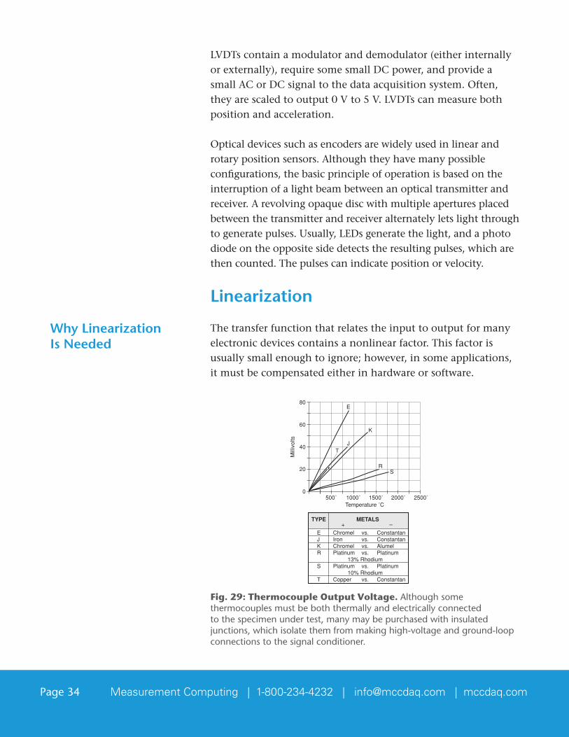
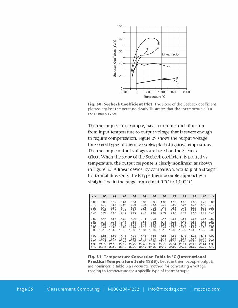
Thermocouples, for example, have a nonlinear relationship from input temperature to output voltage that is severe enough torequirecompensation.Figure29showstheoutputvoltagefor several types of thermocouples plotted against temperature. Thermocouple output voltages are based on the Seebeck effect. When the slope of the Seebeck coefficient is plotted vs. temperature, the output response is clearly nonlinear, as shown inFigure30.Alineardevice,bycomparison,wouldplotastraighthorizontal line. Only the K type thermocouple approaches a straightlineintherangefromabout0°Cto1,000°C.
Figure 5.31
mV
0.000.100.200.300.40
0.500.600.700.800.90
1.001.101.201.301.40
.00
0.001.703.405.096.78
8.4710.1511.8213.4915.16
16.8318.4820.1421.7923.44
.01
0.171.873.575.266.95
8.6310.3111.9913.6615.33
16.9918.6520.1321.9623.60
.02
0.342.043.745.437.12
8.8010.4812.1613.8315.49
17.1618.8220.4722.1223.77
.03
0.512.213.915.607.29
8.9710.6512.3213.9915.66
17.3218.9820.6422.2923.93
.04
0.682.384.085.777.46
9.1410.8212.4914.1615.83
17.4919.1520.8022.4524.10
.05
0.852.554.255.947.62
9.3110.9812.6614.3315.99
17.6619.3120.9722.6224.26
.06
1.022.724.426.117.79
9.4711.1512.8314.4916.16
17.8219.4821.1322.7824.42
.07
1.192.894.586.277.96
9.6411.3212.9914.6616.33
17.9919.6421.3022.9424.59
.08
1.363.064.756.448.13
9.8111.4913.1614.8316.49
18.1519.8121.4623.1124.75
.09
1.533.234.926.618.30
9.9811.6513.3314.9916.66
18.3219.9721.6323.2724.92
.10
1.703.405.096.788.47
10.1511.8213.4915.1616.83
18.4820.1421.7923.4425.08
mV
0.000.100.200.300.40
0.500.600.700.800.90
1.001.101.201.301.40
Temperature Conversion Table in ˚C (IPTS 1968)
Figure . .5
Fig. 31: Temperature Conversion Table in °C (International Practical Temperature Scale 1968). Because thermocouple outputs are nonlinear, a table is an accurate method for converting a voltage reading to temperature for a specific type of thermocouple.
Page 36 Measurement Computing | 1-800-234-4232 | [email protected] | mccdaq.com
ThecurveinFigure30showsthatoneconstantscalefactorisnot sufficient over the entire temperature range for a particular thermocouple type to maintain adequate accuracy. Higher accuracy comes from reading the thermocouple voltage with a voltmeter and applying it to the thermocouple table from the National InstituteofStandardsandTechnology(NIST)showninFigure31.Acomputer-baseddataacquisitionsystem,incontrast,automatesthe temperature-conversion process using the thermocouple voltage reading and an algorithm to solve a polynomial equation. Equation 5 describes this relationship as follows:
T = ao+a1x+a2x2+a3x3+...anxn
Where:T = temperature, °Cx = thermocouple voltage, Va = polynomial coefficients unique to each type of thermocouplen = maximum order of the polynomial
Equation 5: Temperature Polynomial.
Theaccuracyincreasesproportionallytotheorderofn.Forexample,whenn=9,a±1°Caccuracymayberealized.Butbecause high-order polynomials take time to process, lower orders may be used over limited temperature ranges to increase the processing speed.
Figure 5.32 (6.04 B)
NIST Polynomial CoefficientsTYPE E TYPE J TYPE K TYPE R TYPE S TYPE T
Nickel-10% Chromium(+) Iron (+) Nickel-10% Chromium (+) Platinum-13% Rhodium (+) Platinum-10% Rhodium Copper (+)Versus Versus Versus Nickel-5% (–) Versus Versus Versus
Constantan (–) Constantan (–) (Aluminum Silicon) Platinum (–) Platinum (–) Constantan (–)
-100 ˚C to 1000 ˚C 0 ˚C to 760 ˚C 0 ˚C to 1370 ˚C 0 ˚C to 1000 ˚C 0 ˚C to 1750 ˚C -160 ˚C to 400 ˚C±0.5 ˚C ±0.1 ˚C ±0.7 ˚C ±0.5 ˚C ±1 ˚C ±0.5 ˚C
9th order 5th order 8th order 8th order 9th order 7th order
0.104967248 -0.048868252 0.226584602 0.263632917 0.927763167 0.10086091017189.45282 19873.14503 24152.10900 179075.491 169526.5150 25727.94369-282639.0850 -218614.5353 67233.4248 -48840341.37 -31568363.94 -767345.829512695339.5 11569199.78 2210340.682 1.90002E + 10 8990730663 78025595.81
-448703084.6 -264917531.4 -860963914.9 -4.82704E + 12 -1.63565E + 12 -92474865891.10866E + 10 2018441314 4.83506E + 10 7.62091E + 14 1.88027E + 14 6.97688E + 11-1.76807E + 11 -1.18452E + 12 -7.20026E + 16 -1.37241E + 16 -2.66192E + 131.71842E + 12 1.38690E + 13 3.71496E + 18 6.17501E + 17 3.94078E + 14-9.19278E +12 -6.33708E + 13 -8.03104E + 19 -1.56105E + 192.06132E + 13 1.69535E + 20
Temperature Conversion Equation: T = a0 + a1x + a2x2 + ...+ anxn
Nested Polynomial Form: T = a0 + x(a1 + x(a2 + x(a3 + x(a4 + a5x)))) (5th order)
a0a1a2a3a4a5a6a7a8a9
Fig. 32: NIST Polynomial Coefficients. The NIST polynomial table is a more accurate means of calculating a linearizing function for a particular thermocouple than a single coefficient, even though it uses a polynomial equation.
Page 37 Measurement Computing | 1-800-234-4232 | [email protected] | mccdaq.com
Figure 5.33
Voltagea
Tem
p
Ta = bx + cx2 + dx3
Fig. 33: Curve Divided into Sectors. Although a computer usually finds the solution to the NIST polynomial, breaking the curve into sections representing lower-order polynomials can accelerate the process.
The polynomials in the data acquisition system’s computer calculate the real temperature for the thermocouple voltage. Typically, the computer program handles a nested polynomial to speed the process rather than compute the exponents directly. Nested polynomials are the only practical way of dealing with complicated equations. Without such techniques, large state tables with more than a few hundred entries are difficult to handle.(SeeFigure32.)Also,high-orderpolynomialscanbecomputed faster when the thermocouple characteristic curve can be divided into several sectors and each sector approximated byathird-orderpolynomialasshowninFigure33.
Hardware also may be designed to accommodate the nonlinearity of a thermocouple, but the circuitry becomes complex and expensive in order to reduce its susceptibility to errors from outside influences such as electrical noise and temperature variations within the circuits. The compensating circuitry is nonlinear and contains breakpoints programmed with diodes, resistors, and reference voltages, all subject to errors that are avoided in software compensation methods. However, several modules are commercially available with excellent, stable, built-in linearizing circuits. The thermocouple voltage is extremely low, and most signal conditioners concentrate less on compensation and more on amplifying the signal while rejecting common-mode noise. Alternativedigitalhardwaremethodsusealook-uptabletoconvertthe thermocouple voltage to a corresponding temperature.
Software Linearization
Hardware Linearization
Page 38 Measurement Computing | 1-800-234-4232 | [email protected] | mccdaq.com
Inputs
DC/DC5 VDC
–15 +15 +5
To DC/DC convertersin each channel
9-20VDCsupply
EnbAddrOut
Mux
Gainconfig.
µP
DC/DC
IsolationCh 0
IsolationCh 1
IsolationCh 2
IsolationCh 3
IsolationCh 4
IsolationCh 5
IsolationCh 6
IsolationCh 7 Wide range
regulator
Bypass
Input
Isolationamplifier
Isolated supplyDC/DC
2-bit opto-iso
Toanalogmux
Fromon-boardµP
5 VDC+15–15
Lowpassfilter
2
Figure 5.34
Programmableattenuator
andamplifier
I/O
Fig. 34: Isolation from High Voltage. The isolated voltage-input modules let data acquisition systems isolate several channels of analog input, up to 500 V channel-to-channel and channel-to-system.
Circuit Protection
Many data acquisition systems contain solid-state multiplexing circuits to rapidly scan multiple input channels. Their inputs are typically limited to less than 30 V and may be damaged when exposed to higher voltages. Other solid-state devices in a measurement system including input amplifiers and bias sources also are limited to low voltages. However, these inputs can be protected with a programmable attenuator and isolation amplifiers that isolate the high-voltage input stage from the solid-statecircuitry.(SeeFigure34.)
Anotherconsiderationoftenoverlookedisconnectingactiveinputs to an unpowered data acquisition system. Common safety practice calls for all signals connected to the input of the unpowered data acquisition system to be disconnected or theirpowerremoved.Frequently,de-energizeddataacquisitionsystem signal conditioners have substantially lower input impedances than when energized, and even low-voltage
Hazards to Instrumentation Circuits
Page 39 Measurement Computing | 1-800-234-4232 | [email protected] | mccdaq.com
input signals higher than 0.5 VDC can damage the signal conditioners’ input circuits.
Figure 5.35 A
Output–
+
+V
-V
1 kΩ
A
D1
D2
Inputsignal
Circuit A
Figure 5.35 B
Output–
+
2 kΩ
D S
G
FETInputsignal A
Circuit B
Fig. 35: Overload Protection. Certain CMOS multiplexers may be protected against overvoltage destruction with diode and resistor networks that shut down any parasitic transistors in the device, limit the current input to a safe level, and shunt input signals to ground when the power supplies are turned off (Circuit A). Junction gate field-effect transistors (JFETs) also protect multiplexer inputs when they are connected as diodes. The JFET clamps at about 0.6 V, protecting the sensitive op amp input from destruction (Circuit B).
Several methods are used to protect signal conditioner inputs from damagewhenexposedtotransientsof10Vto100V.Often,a1,000Ω, current-limiting resistor is in series with the input when novoltageisappliedtotheIAs’input.Fortransientinputvoltagesto 3,000 V and higher, a series resistor and a transient voltage suppressorareinstalledacrosstheinputterminals.(SeeFigure35.)
Electrostatic discharge (ESD) damage can be avoided by handling individual circuit boards carefully and providing proper shielding. ESD comes from the static charge accumulated on many different kinds of materials, which finds a return to ground or a mass that attracts the excess electrons. The charge can create potential differences that can eventually arc over largedistances.Anarccontainingonlyseveralmicrojoulesof energy can destroy or damage a semiconductor device. GroundingaloneisnotsufficienttocontrolESDbuildup;itonly ensures that all conductors are at the same potential.
Overload Protection
ESD Protection
Page 40 Measurement Computing | 1-800-234-4232 | [email protected] | mccdaq.com
Controllinghumiditytoabout40%andslightlyionizingtheairare the most effective methods of controlling static charge.Adischargecantravelonefootinonenanosecondandcouldriseto5A.Anumberofdevicessimulateconditionsforstaticdischarge protection, including a gun that generates pulses at a fixed voltage and rate. Component testing usually begins with relatively low voltages and gradually progresses to higher values.
Conclusion
Knowing all the tools available for signal conditioning helps you make well-informed decisions when putting together a data acquisition system. To streamline this process, Measurement Computing Corporation (MCC) offers best-in-class data acquisition hardware to end users for all types of industries.
Asexpertsinthedataacquisitionmarket,MCCspecializesindelivering high-accuracy signal conditioning options on all of their measurement devices with interfaces that include USB, Ethernet,Wi-Fi,andstand-aloneloggers.AllMCCproductsalsocome with easy-to-use and efficient device drivers and application software to support both programmers and non-programmers.
Known for simple installations, lifetime warranties, and free live technical support, MCC products provide the highest quality for thebestprice.LetMCChelpyoufindtherightdeviceforyourspecific measurement and application needs.
For more information on our signal conditioning products, please visit www.mccdaq.com.
Page 41 Measurement Computing | 1-800-234-4232 | [email protected] | mccdaq.com
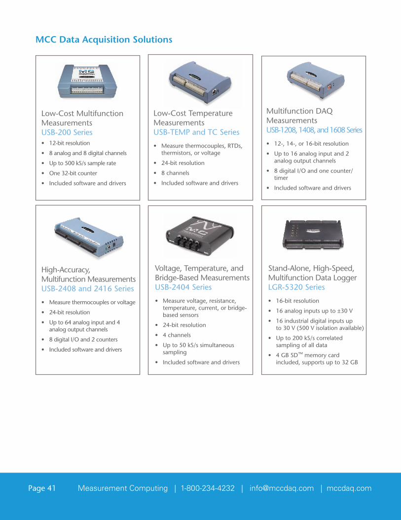
Low-Cost Multifunction Measurements USB-200 Series• 12-bitresolution
• 8analogand8digitalchannels
• Upto500kS/ssamplerate
• One32-bitcounter
• Includedsoftwareanddrivers
Low-Cost Temperature MeasurementsUSB-TEMP and TC Series
• Measurethermocouples,RTDs,thermistors, or voltage
• 24-bitresolution
• 8channels
• Includedsoftwareanddrivers
Multifunction DAQ MeasurementsUSB-1208, 1408, and 1608 Series
• 12-,14-,or16-bitresolution
• Upto16analoginputand2analog output channels
• 8digitalI/Oandonecounter/timer
• Includedsoftwareanddrivers
High-Accuracy, Multifunction MeasurementsUSB-2408 and 2416 Series
• Measurethermocouplesorvoltage
• 24-bitresolution
• Upto64analoginputand4analog output channels
• 8digitalI/Oand2counters
• Includedsoftwareanddrivers
Voltage, Temperature, and Bridge-Based MeasurementsUSB-2404 Series
• Measurevoltage,resistance,temperature, current, or bridge-based sensors
• 24-bitresolution
• 4channels
• Upto50kS/ssimultaneoussampling
• Includedsoftwareanddrivers
MCC Data Acquisition Solutions
Stand-Alone, High-Speed, Multifunction Data LoggerLGR-5320 Series
• 16-bitresolution
• 16analoginputsupto±30V
• 16industrialdigitalinputsup to 30 V (500 V isolation available)
• Upto200kS/scorrelated sampling of all data
• 4GBSD™ memory card included, supports up to 32 GB