Embed Size (px)
Citation preview
UNIVERSITY OF hJ-IVVAIl LIBRARY
DYNAMIC ADAPTABLE ANTENNA ARRAYS FOR WIRELESS
COMMUNICATION NETWORKS
A THESIS SUBMI'ITED TO THE GRADUATE DMSION OF THE UNIVERSITY OF HAW AI'I IN PARTIAL FULFILLMENT
OF THE REQUIREMENTS FOR THE DEGREE OF
MASTER OF SCIENCE
IN
ELECTRICAL ENGINEERING
AUGUST 2006
By Justin Roque
Thesis Committee:
Wayne A. Shiroma, Chairperson TepDobry
Eric L. Miller

We certify that we have read this thesis and that, in our opinion, it is satisfactory in scope
and quality as a thesis for the degree of Master of Science in Electrical Engineering.
THESIS COMMITTEE
Chairperson
ii

I dedicate this thesis to my family.
To my Mom, Dad, Brother, and Lauren who have supported me with unconditional love
and support throughout the long college road that I have taken.
iii

ACKNOWLEDGEMENTS
First of all I would like to acknowledge Dr. Wayne Shiroma for giving me the
opportunity to join his research group and further my education. The interesting work,
conferences, and papers we have published would have not been possible without the
commitment and enthusiasm that he has shared with all of his students.
Next I would like to thank the committee members Dr. Dobry and Dr. Miller. Dr.
Dobry for his guidance through my undergraduate studies and whose EE260 class has
kept me motivated to stick with electrical engineering. Dr. Miller for his passion for
engineering will continue to influence many more undergraduate and graduate electrical
engineers in their academic careers.
I would like to thank my fellow researchers. I have had the opportunity to work
with "two sets" ofMMRL groups. The first being the era of Dr. Ryan Miyamoto, I have
learned a lot from his guidance and would like to thank him for his patience and teaching.
To the members of the MMRL group during this period, Kendall Ching, Blaine
Murakami, Stephen Sung, Joe Cardenas. TJ Mizuno, and Cheyan Song I would like to
thank you for all the support and encouragement that has allowed me to get this far. A
thank you to the present members of the MMRL group, Brandon Takase. Ryan Pang,
Justin Akagi, and Monte Watanabe whom I know will carry research to the next level. A
special thanks to Grant Shiroma who has taken the role of mentor to the present members
of the MMRL group and has always helped me when I was in a bind.
iv

Lastly, I would like to thank the sponsors for all the research done in this thesis.
Funding was provided by the following sponsors AFRL, NASA, AFOSR, AlAA, NGST,
and Oceanit Laboratories.
v

ABSTRACf
Many wireless systems are being incorporated into a single device. Combining
different wireless systems in one package simplifies circuitry, increases efficiency and
allows users to use one interface to access many systems. Phased arrays and
retrodirective arrays improve the perfonnance at the antenna front end. Reconfigurable
networks eliminate redundant circuitry in the wireless subsystems and allow sharing of
specific components.
This thesis presents advances in satellite-ta-satellite communication systems,
mobile terrestrial to satellite systems, and a method of characterizing a class of
reconfigurable circuits. First, a two-dimensional retrodirective array using quadruple
subhannonic mixing is designed at 10.5 GHz for satellite-to-satellite communication.
Two small satellites demonstrated a retrodirective link with tracking ranging from -40· to
40·. Secondly, a two-dimensional transmit frequency-controlled phased array is
presented. Simple voltage controlled steering of the phased array makes for easy
integration with external tracking and control systems. A scanning range of 40· per axis
has been demonstrated. Lastly a method for characterizing a reconfigurable MEMS
tunable matching network has been presented and verified by circuit simulation. As more
systems require communication at different frequencies, variable-frequency components
require using tunable matching networks. Characterization of the matching networks
becomes an issue when troubleshooting modules within wireless communication devices.
vi
TABLE OF CONTENTS
CHAPTER
1. INTRODUCTION .............. _ ........ _ ... __ ........... ___ ............... _ ............................ 1
1.1 Omnidireetional Antennas ..................................................................... _ ........ 3
1.2 Phased Arrays ................................................................................................... 4
A. Conventional Phased A"Q)' Methods ............................................................. 5
B. Frequency-Scanned Phased A"Q)'s ................................................................ 5
C. Frequency-Controlled Phased A"Q)'s ............................................................ 6
1.3 Retrodirective Arrays ....................................................................................... 8
A. Corner Ref/ector ............................................................................................. 8
B. Van Ana A"Q)' ................................................................................................ 8
C. Phase-Co,yugating A"Q)' ............................................................................... 9
1.4 Retrodirective Arrays for Small-Satellite Networks .............................. _ .. 10
1.5 Mobile Communication Arrays ................ _ .................................................. 11
1.6 Reconfigurable Networks ............................................................................... 12
1.7 Organiza.tion of Thesis .............................................................................. _. 14
2. RETRODIRECTIVE ANTENNA ARRAYS FOR USE IN
SMALL SATELLITE NETWORKS ....................... _ ................................. _ ........ 15
2.1 Introduction ............ _ ........... _ .... _ .................................................................... 15
2.2 Design Para.meters .• _ ................. _ .................................................................. 15
2.3 Mixing Techniques ................................................................................. _ ....... 18
A. Fundamental Mixing Technique ................................................................... 18
B. Subhormonic Mixing Technique ................................................................... 19
vii

C. Quadruple Subharmonic Mixing Technique ................................................. 20
2.4 Retrodirective Circnitr)" ................................................................................. 22
A. Mixer Array Design ...................................................................................... 22
B. Antenna Array ............................................................................................... 24
C. Oscillator ...................................................................................................... 28
2.5 Interrogator and Receiver Circuitry' ............................................................. 29
2.6 Retrodirective Charaderization .................................................................... 35
2.7 Experimental ResuIts ............................................... _ ................................... 37
2.7.1 Two-dimensional Measurements ........................................................... 38
2.7.2 ContinDoos Wave Power Measurements .............................................. 40
A. Bistatic Measurements .................................................................................. 41
B. Monostatic Measurements ............................................................................ 43
C. Interrogator/Receiver Measurements ........................................................... 44
3. FREQUENCY-CONTROLLED PHASED ARRAyS ........................................... 48
3.1 Introduction ..................................................................................................... 48
3.2 One-Dimensional FuD-Duplex, Voltage-ControDed Phased Array .•.•••.•.••• 50
3.2.1 Design Parameters .................................................................................. 50
3.2.2 One-Dimensional Freqneney-ControDed Circuitry and Design.M ••• M. 52
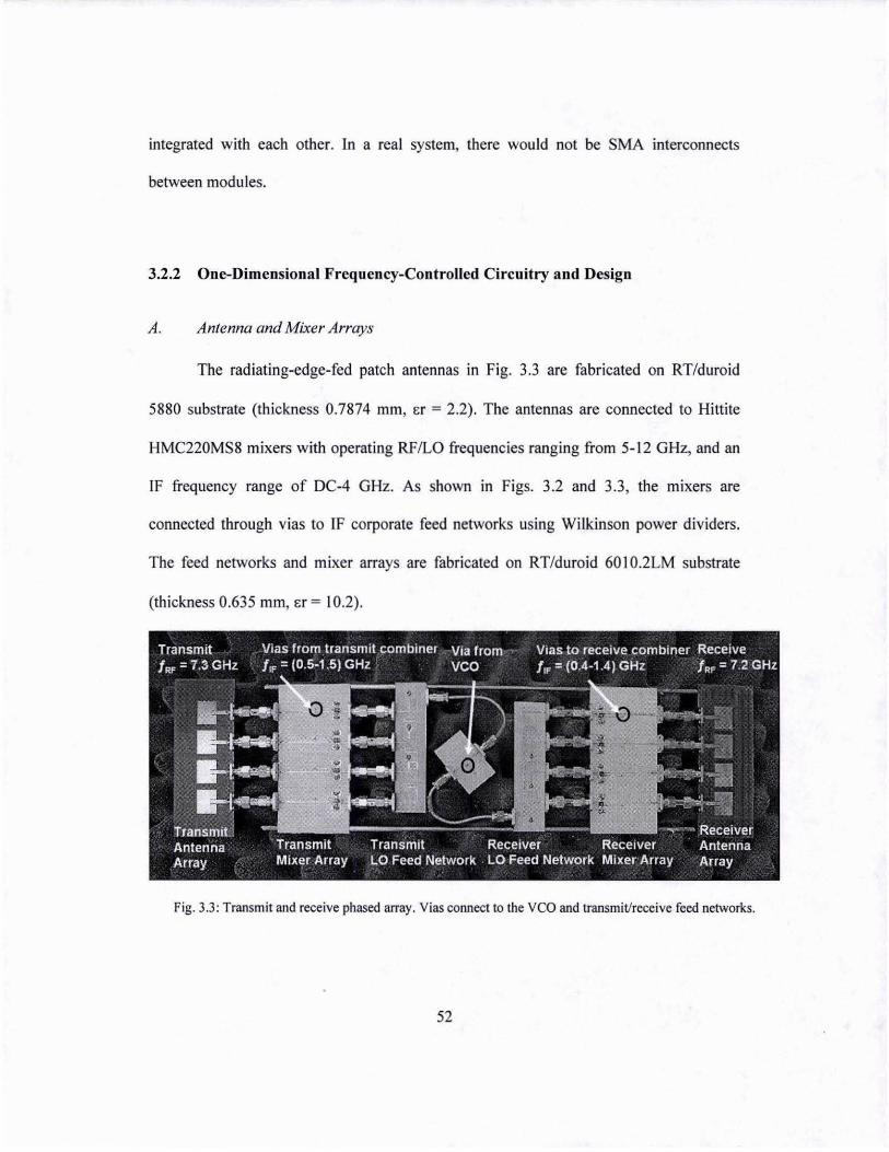
A. Antenna and Mixer Arrays ............................................................................ 52
B. Phase-Delay LO Feed Network .................................................................... 53
C. Transmitter, Receiver, and VCO Circuitry ................................................... 55
3.3 Experimental Results for One-Dimensional Array •. _ ................................. 55
3.4 Two-Dimensional Transmit, Voltage-ControDed Phased Array •••••• "" ....... 58
viii

3.4.1 Two-Dimensional Bea.m Steering ....... _ ................................................ 58
3.4.2 Design Parameters .................................................................................. 60
3.4.3 Two-Dimensional Freqnency-Controlled Cirenit Design .................... 60
A. Antenna Array ............................................................................................... 61
B. Phase Addition Mixer array and Wilkinson power dividers ......••••••............. 62
C. IF transmit control board ............................................................................. 64
D. LO control board .......................................................................................... 65
3.4 Experimental Resnlts for Two-Dimensional Array ....................... _ ........... 67
4. CHARACTERlZATION OF RECONFIGURABLE
AMPLIFIER NETWORKS ..................................................................................... 70
4.1 Introduc:tion ..................................................................................................... 70
4.2 TITL Charac:teriza:tion Tbeor)' ..................................................................... 73
4.3 SymboHc Analysis ........ __ ............................................................................. 76
4.4 Simulation and Analysis ................................................................................. 78
4.5 Applications .............. _ ......................... _ ....................................................... 80
A. Determining the Value of Cswltch ................................................................... 80
B. Testingfor Faulty Switches in the TITL ........................................................ 82
5. CONCLUSIONS AND FUTURE WORK .............................................................. 83
5.1 Conc:lusions ................................ ___ ........................................................... 83
5.2 Suggestions for Future Work. .................... _ ................................................ 84
A. Two-dimensional Full-duplex Frequency-Controlled Phased Array ......••.•. 84
B. Retrodirective Frequency-Controlled Array Using Phase Detection ....•••.••. 86
C. Retrodirective Frequency-Controlled Array Using Power Detection .......... 87
ix

APPENDIX A - MA TLAB Code for TITL CharacferizatioD_. ___ ......... __ •• _ ••• __ ••• 90
REFERENCES ........................... __ ................................................................................. 94
x

LIST OF TABLES
Table 4.1: ABeD parameters of switch states .................................................................. 75
Table 4.2: Possible combinations of two switches in the TITL ........................................ 77
Table 4.3: Complex gain of amplifier circuitry from ADS simulation a .......................... 80
xi

LIST OF FIGURES
1.1: Picture of the Mobile Modular Command Center (M2C2) ......................................... 2
1.2: (a) Basic wireless communication system with single omnidirectional antenna •...•.... 3
1.3: Omnidirectional antenna radiating power in all directions .......................................... 4
1.4: ConventionallllTllY using phase shifters ...................................................................... 5
1.5: Figure of frequency scanned lIITIIy ............................................................................... 6
1.7: Comer Reflector .......................................................................................................... 8
1.8: Schematic ofYan Atta Array ....................................................................................... 9
1.9: Phase Conjugating lIITIIy ............................................................................................ 10
1.10: Picture ofM2C2 with external satellite dish ........................................................... 12
1.11: Photographs ofMEMS switches in matching networks [IS] .................................. \3
2.1: Schematic of satellite communication link ................................................................ 16
2.2: Pair of experimental nanosate11ites ............................................................................ 16
2.3: (a) Phase conjugating lIITIIy using heterodyne mixers at each element ..................... 17
2.4: (a) Diode mixing circuit fed by voltage source, (b) IN characteristic of diode ........ 18
2.5: (a) Basic mixer circuit, (b) Block diagram of quadruple subharmonic mixer ........... 23
2.6: (a) Mixer IIITIIY, (b) Single mixer ............................................................................... 24
2.7: Patch antenna element ............................................................................................... 25
2.8: Reflection Coefficient of patch antenna .................................................................... 26
2.9: E-plane simulated (Ansoft Ensemble) and experimental Axial Ratio (AR) .............. 26
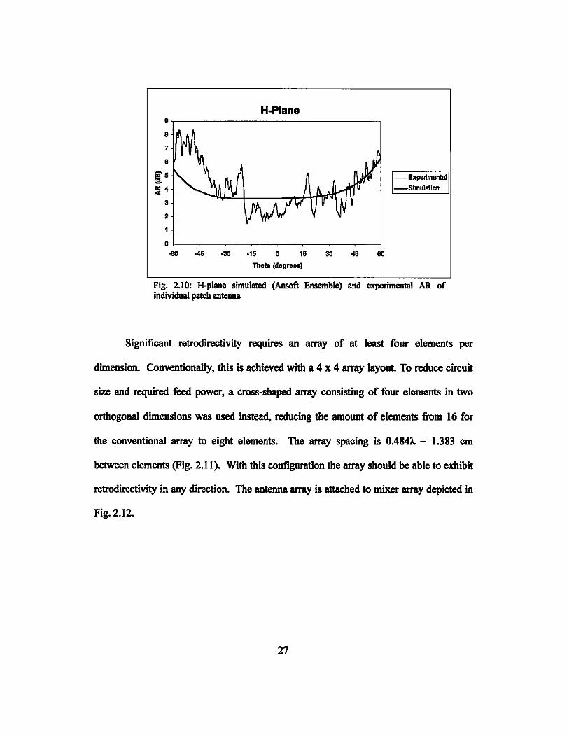
2.10: H-plane simulated (Ansoft Ensemble) and experimental AR ................................. 27
2.11: Circularly polarized cross-shaped microstrip patch antenna lIITIIy .......................... 28
2.12: Photograph of antenna and mixer lIITIIy ................................................................... 28
xii

2.13: Pictures of the Oscillator .......................................................................................... 29
2.14: (a) Communication link between retrodirective array and interrogator .................. 30
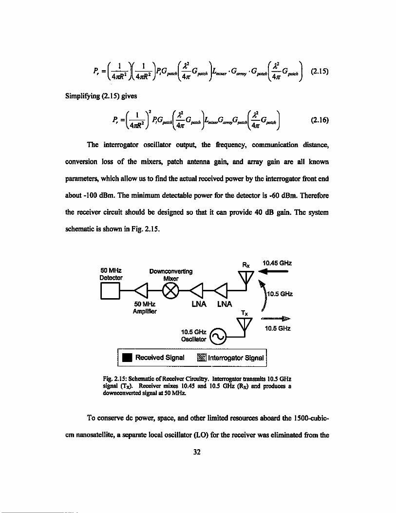
2.15: Schematic of Receiver Circuitry .............................................................................. 32
2.16: (a) Receiver circuit board layout, (b) Interrogator and receiver .............................. 34
2.17: Downverting mixer using Agilent 8202 diode ........................................................ 34
2.16: Picture of coupled patched antenna mounted on satellite ........................................ 35
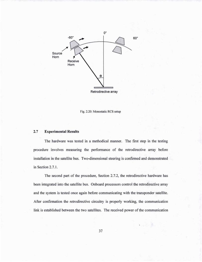
2.19: Bistatic RCS setup ................................................................................................... 36
2.20: Monostatic RCS setup ............................................................................................. 37
2.21: Bistatic RCS taken along 45' plane of antenna array .............................................. 38
2.22: RCS of the retrodirective array with source hom at O· ............................................ 39
2.23: RCS of the retrodirective array with source hom at -20' ........................................ 39
2.23: RCS of the retrodirective array with source hom at -20' ........................................ 39
2.24: RCS ofretrodirective array with source hom at +20' ............................................. 40
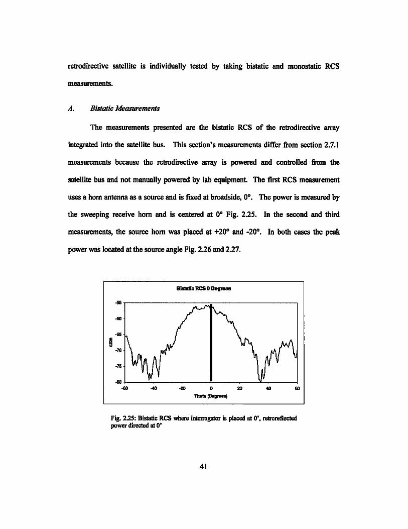
2.25: Bistatic RCS at 0' .................................................................................................... 41
2.25: Bistatic RCS at 0' ................................. : .................................................................. 41
2.26: Bistatic RCS at +20' ................................................................................................ 42
2.26: Bistatic RCS at +20' ................................................................................................ 42
227: Bistatic RCS at -20' ................................................................................................. 42
2.26: Bistatic RCS at +20' ................................................................................................ 42
2.28: Monostatic RCS of the retrodirective array ............................................................. 43
2.29: Fixed beam RCS of antenna array ........................................................................... 44
2.30: Voltage output of the power detector as a function of input power ....................... : 45
2.31 Monostatic RCS using detector output power .......................................................... 46
xiii

2.32: Retrodirective to retrodirective link ......................................................................... 47
3.1: General heterodyne-scan phased-array architecture ....•...........................••••...•....•••••. 49
3.2: Full-duplex frequency-controlled phased-array architecture ..................................... 51
3.3: Transmit and receive phased array ............................................................................ 52
3.4: Four-element LO feed network with a progressive phase delay of ~ = 4" ................ S4
3.5: Measured insertion loss of the four-element LO feed network ................................. S4
3.6: Measured phase response of the 4-element LO network ........................................... 55
3.7: Transmitter. receiver. and veo circuitry .................................................................. S6
3.8: Receiver radiation patterns vs. veo tuning voltage ................................................. S7
3.9: Transmit radiation patterns vs. veo tuning voltage ................................................. S7
3.10: Phase addition for achieving two-dimensional steering [1] ..................................... 59
3.1 I: Block diagram of two-dimensional voltage controlled array system ...................... 60
3.1 2: Board level design schematic .................................................................................. 61
3.13: Picture of antenna array ........................................................................................... 62
3.14: Schematic of mixer board array •.............................................................................. 63
3.15: Phase addition schematic substituted into block diagram of Fig. 3.1 I .................... 64
3.16: Schematic ofIP transmit and IP receive beam control board .................................. 65
3.17: Schematic ofLO control board ................................................................................ 66
4.1: Schematic of unknown device with input and output matching networks ................ 70
4.2: (a) Top view of basic MEMS switch, ........................................................................ 72
4.3: Schematic ofTlTL network ....................................................................................... 73
4.4: Shunt element with associated ABeD parameters [6] ............................................... 74
4.5: Model ofindividual MEMS switch ........................................................................... 74
xiv

4.6: S parameters of entire TITL ....................................................................................... 75
4.7: Schematic of circuit S parameters, ............................................................................ 76
4.8: TITL with N-switches ................................................................................................ 77
4.9: (a) Switch ION, Switch 2 OFF ................................................................................. 78
4.10: ADS simulation schematic ofTITL ......................................................................... 79
4.11: (a) First two switches used to get 3 unique combinations ....................................... 81
5.1: Transmit and receive IF control boards ..................................................................... 85
5.2: Transmit and receive LO control boards .................................................................. 85
5.3: Schematic of two-dimensional full-duplex frequency-controlled array .................... 86
5.4: Proposed schematic for phase detecting control circuitry ......................................... 87
5.5: Proposed schematic for power detecting controL ..................................................... 88
5.6: (a) Receive power with one main lobe and V STEER graph ......................................... 89
xv
CHAPTER 1
INTRODUCTION
A large number of today's communication systems consist of groups of smaller
subsystems linked together in one form or another. The most common example of this is
a cellular phone communication system. Cellular phones have made it possible to
communicate with people on the other side of the globe. Following the path of the
cellular phone signal, up to three types of wireless communication systems are used.
The first is the connection of the mobile transponder to the local service provider tower.
Second, the tower is linked to a mainframe and the signal is transmitted to orbiting
satellites. Lastly, the satellite may have to relay the signal to another orbiting satellite
and have the signal transmitted back to a ground station on the other side of the world. In
this example, three wireless paths are evident, a mobile terrestrial to fixed terrestrial
system, a terrestrial to satellite system, and a satellite-to-satellite system.
Companies such as DirectTV and Wildblue are investing $1.4 billion into the
latest communication satellites, SPACEWAY 1 & 2 [1], [2]. The SPACEWAY
broadband satellite network hopes to provide not only voice communication, but high
speed communications for internet, data, video, and multimedia applications [3].
Another example of combining multiple wireless communication systems and
applications is the military's Mobile Modular Command Center (M2C2), Fig. 1.6 [4].
Hawaii technology companies are combining efforts to outfit a Humvee with radio and
1
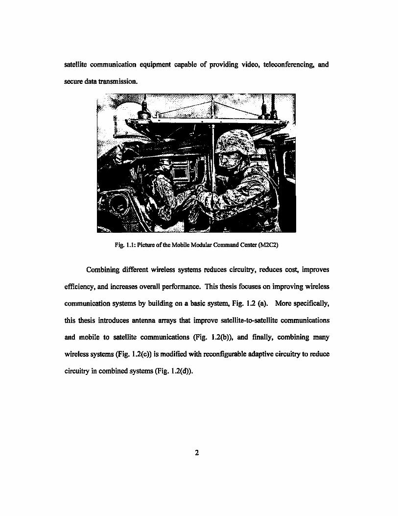
satellite communication equipment capable of providing video, teleconferencing, and
secure data transmission.
Fig. 1.1: Picture of me Mobile Modular Command Center (M2C2)
Combining different wireless systems reduces circuitty, reduces cost, improves
efficiency, and increases overall performance. This thesis focuses on improving wireless
communication systems by building on a basic system, Fig. 1.2 (a). More specifically,
this thesis introduces antenna arrays that improve satellite-to-satellite communications
and mobile to satellite communications (Fig. 1.2(b», and finally, combining many
wireless systems (Fig. 1.2(c» is modified with reconfigurable adaptive circuitty to reduce
circuitty in combined systems (Fig. 1.2(d».
2
Oata WIRELESS
COMMUNICATION I-_.J SYSTEM
(a)
_...,.111 1"'------------, • • • • • • • • • • : :. 0:==-1 r:--::--::--, : : • AmpIl!IcaIIon I ••
L..::=~JL __ ..... ~(1.;.1 S+--""l... .J.. _______ :
• • • . : . : · : • • - : 8I:!Ige (N) : :
1,.------------,
(c)
.------------1 I I I I I I I I I I I I I I I I I I
~~ I I ~CAnoN~----~.l :
SYSTEM I Data
L ____________ I AnIenna_
(b)
-(d)
Fig. 1.2: (a) Basic wireless ccmmtmlcatlon system with single omnidin:etional antenna, (b) Antenna array c:ircuitry added to basic wireless system, (c) N wireless ccmmtmlcatlon systems, (d) N wireless ccmmtmlcatlon systems sharing amplification stage and antenna array
1.1 Omnidirectional Antennas
Omnidirectional antennas are the simplest and most common means for
broadcasting electromagnetic waves into free space. Fig. 1.3 depicts an omnidirectional
antenna and its propagation characteristics. Single-wire construction makes this type of
antenna cost effective. The electromagnetic signals radiate in all directions allowing
users to communicate with one another without knowing the positions of other user
antennas.
3
Fig. 1.3: Omnidirectional antenna radiating power io all directions
An omnidirectional antenna may be a cost-effective solution for commercial
applications. However, there are downsides associated with broad radiation patterns. In
transmission, power is radiated inefficiently in all directions. The signal can possibly
interfere with other systems and is susceptible to eavesdropping. In reception, signals in
all directions including interference and jamming signals are received. These
characteristics cause vulnerabilities in a security-sensitive communication system.
1.2 Phased Arrays
The efficiency and security of a wireless system is greatly increased if the power
transmitted by an antenna is focused only on the target. The easiest method of focusing
electromagnetic power is manipulating the phases of antenna arrays. Typical phased
arrays produce focused beams significantly reducing receive and transmit interference
and allows controllable electronic steering.
4
A. Conventional Phosed AmI)' Methods
Phased arrays are the simplest method of beam forming. In Fig. 1.4 each antenna
element is connected to a phase shifter. To steer the beam the phase shifters delay the
signal and a phase progression from element to element will steer the beam. The
downside of the conventional phased array is the expensive phase shifters this method
requires. In large arrays, the phase shifter control circuitry can become complex.
Fig. 1.4: Conventional array using phase shifters
B. Frequency-ScCI1'ITIed Phosed A"Q)'s
Targsllocated W tl> the right I
One of the drawbacks in conventional phased-array antenna systems, especially
large ones, is the cost and complexity associated with individual phase shifters at each
radiating element. An alternative method of beam steering that requires no phase shifter
components, other than fixed delay lines between radiating elements, is the frequency-
5
scanned array [5]. Progressively phased delay lines feed antenna elements. The linear
relationship between frequency and phase in the feed network causes varying phase
progression when tuning the output frequency (Fig. 1.S).
Freq.2 .----· '. · '. • • • • • • \ "-. , , , . , ,
" , "
"""
9+,
Freq.1 Freq.3 _ ........
.' . • • • • • • • • .' . • • • • • • • • • • .. • •
Variable Frequency LOSource
Fig. 1.5: Figure offtequency scanned rmay
C. Frequency-Controlled Phased A"ays
The frequency scanned array is well suited for radar applications, but most
communication systems require a constant transmission frequency. For systems
requiring a fixed radiating frequency, heterodyne mixers can be inserted at each element
6
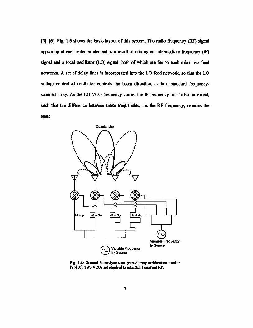
[5], [6]. Fig. 1.6 shows the basic layout of this system. The radio frequency (RF) signal
appearing at each antenna element is a result of mixing an intennediate frequency (IF)
signal and a local oscillator (LO) signal, both of which are fed to each mixer via feed
networks. A set of delay lines is incorporated into the LO feed network, so that the LO
voltage-controlled oscillator controls the beam direction, as in a standard frequency
scanned array. As the LO yeO frequency varies, the IF frequency must also be varied,
such that the difference between these frequencies, i.e. the RF frequency, remains the
same.
.. --.. · '. f .... • • · '. • • • • • • " .. •
\\.
Constant fRF ....- ... ,- .
.' \ , . " . , . , .
• • , . • , ..
,l/~
Fig. 1.6: General heterodyne-scan phased-army architecture used In [7)-[10). Two VCOS are required to maintain a CODSIant RF.
7
1.3 Retrodlrective Arrays
A major disadvantage of phased arrays is that the user must know where to steer
the beam before transmission. A preferred solution is one in which signals can be
transmitted automatically in the same direction as the received signals, a quality
retrodirective arrays provide. On top of self-tracking, both efficiency and security are
increased with negligible increase in circuit complexity.
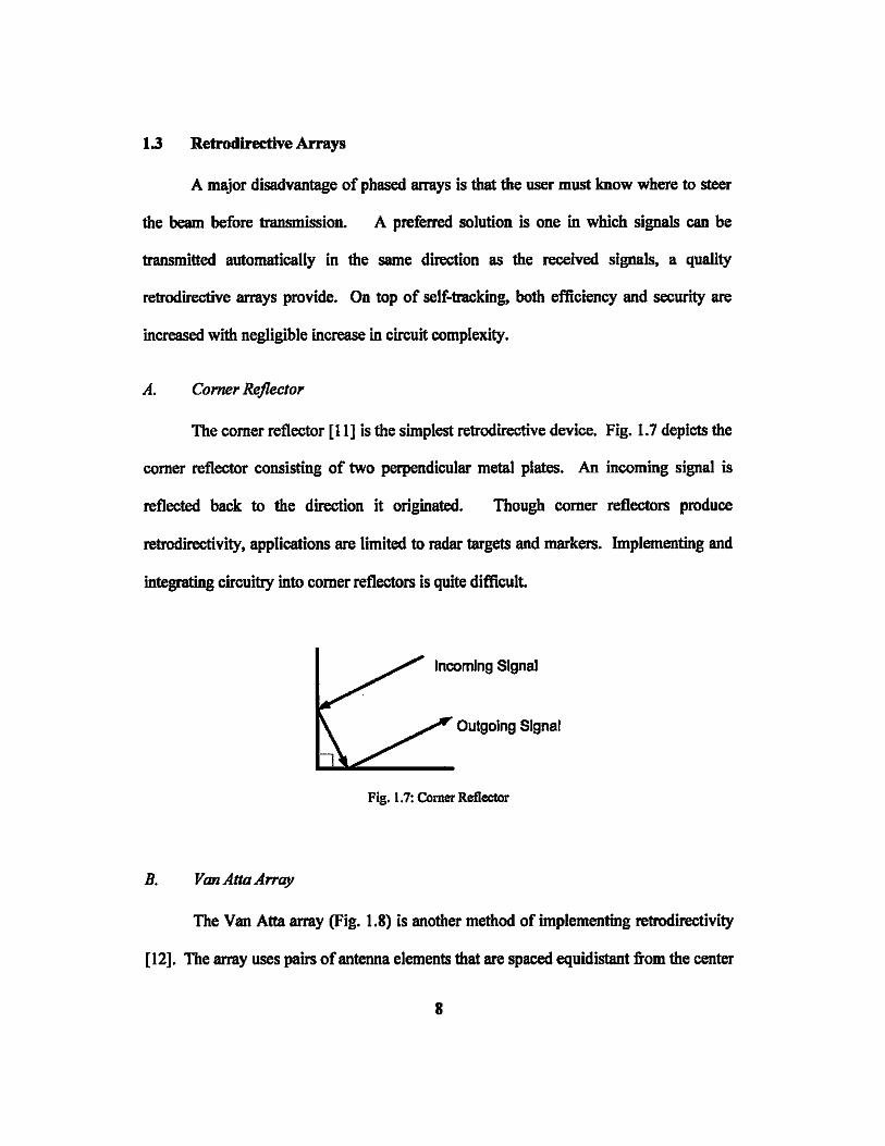
A. Corner Reflector
The comer reflector [II] is the simplest retrodirective device. Fig. 1.7 depicts the
comer reflector consisting of two perpendicular metal plates. An incoming signal is
reflected back to the direction it originated. Though comer reflectors produce
retrodirectivity, applications are limited to radar targets and markers. Implementing and
integrating circuitry into comer reflectors is quite difficult.
Incoming Signal
Outgoing Signal
Fig. 1.7: Comer Reflector
B. Van AttaA"ay
The Van Atta array (Fig. 1.8) is another method of implementing retrodirectivity
[12]. The array uses pairs of antenna elements that are spaced equidistant from the center
8
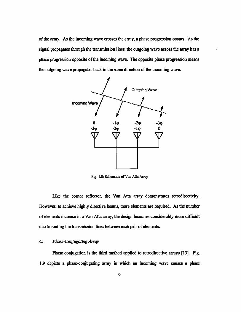
of the array. As the incoming wave crosses the array, a phase progression occurs. As the
signal propagates through the transmission lines, the outgoing wave across the array has a
phase progression opposite of the incoming wave. The opposite phase progression means
the outgoing wave propagates back in the same direction of the incoming wave.
---L~/ _W_ Incoming wi ;········ .......... 1
o -3(jl
I··············f f"
-2(jl
-\ (jl
-3(jl
o
Fig. 1.8: Schematic of Van Alta Array
Like the corner reflector, the Van Atta array demonstrates retrodirectivity.
However, to achieve highly directive beams, more elements are required. As the number
of elements increase in a Van Atta array, the design becomes considerably more difficult
due to routing the transmission lines between each pair of elements.
C. Phose-Conjugating Array
Phase conjugation is the third method applied to retrodirective arrays [13]. Fig.
1.9 depicts a phase-conjugating array in which an incoming wave causes a phase
9
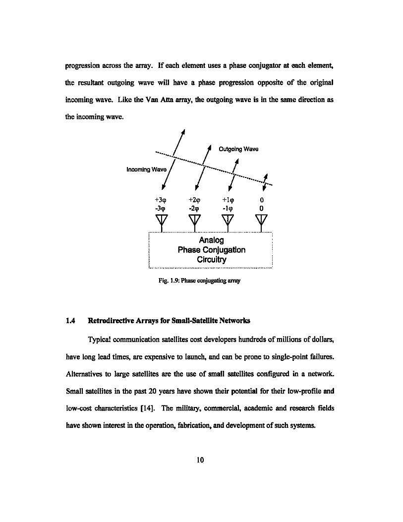
progression across the array. If each element uses a phase conjugator at each element,
the resultant outgoing wave will have a phase progression opposite of the original
incoming wave. Like the Van Atta array, the outgoing wave is in the same direction as
the incoming wave.
__ .~I a __
Incoming Wave / I···~····~ ..... I I l·~·········f.·
+3~ +2~ +1~ 0 .3~ -2~ .1~ 0
, ... I .... _ ...... I ...... _ ..... I ....... _ ... _I_. l Analog . i Phase Conjugation ! Circuitry L~_._ ...•... _ ..... _ ...•• _ ...•. _ ....• _. ____ • ___ • __ . _____ •• _____ ~.~'
Fig. t .9: Phase conjugating array
1.4 Retrodirective Arrays for SmaIl-Satellite Networks
Typical communication satellites cost developers hundreds of millions of dollars,
have long lead times, are expensive to launch, and can be prone to single-point failures.
Alternatives to large satellites are the use of small satellites configured in a network.
Small satellites in the past 20 years have shown their potential for their low-profile and
low-cost characteristics [14]. The militaJy, commercial, academic and research fields
have shown interest in the operation, fabrication, and development of such systems.
10

Small satellites have gained popularity for short-term missions. Experimental
payloads such as sensor testing, communication demonstrations and imaging are a few
experiments being proposed for small-satellite research. These networks also promise
increased mission flexibility by distributing mission task amongst the network. These
networks also reduce the chances of single-point failures. If a node in the network fails,
its tasks can be re-distributed to the other nodes. One of the greatest challenges,
especially in a reconfigurable one, is the communication aspect in which each node must
establish and maintain communications without prior knowledge of each other's location.
One class of small-satellites has dimensions of a lOx lOx 10 em cube.
Conventional propulsion systems are too large to be mounted into small satellites,
making communication between satellites challenging. Self-steering arrays increase
communication efficiency in addition to increasing security. Chapter 2 discusses a small
satellite outfitted with a retrodirective array.
1.S Mobile Communication Arrays
The M2C2 project currently uses a mechanically driven satellite dish mounted on
top of the Humvee, Fig. 1.10. The mechanically driven nature of the satellite dish may be
too slow for the vehicle's constant movement. The large dome also makes the vehicle
conspicuous to enemy forces. Electronically steered phased arrays can provide fast
tracking capabilities than their mechanically driven counterparts. The phased array
circuitry is concealed in the Humvee and only the antenna array is externally mounted.
11

Fig. 1.10: Picture ofM2C2 with external satellite dish
1.6 Rcconfigurable Networks
The M2C2 project mentioned earlier combines many communication systems, all
operating at different frequencies. To reduce circuitry size specific parts of an RF system
can be combined. One specific example is the transmit amplifier at the antenna. To
ensure signal amplitudes are high enough for recoverability the RF signals are amplified.
Amplifiers are the most common method to increase the power of a signal. In most
cases, the amplifier is designed to amplify a specific frequency band. But with modern
technologies merging together a wide frequency spectrum is often preferred. This is
especially true for military applications. Currently separate wireless systems are used
such as a SATCOM system operating at 14.4-15.35 GHz, an enhanced position location
reporting system at 420-450 MHz, cell phone relay capabilities at 1.9 GHz, a secure
wireless LAN at 2.4 GHz, and a GPS tracking system at 1.2 GHz and 1.5 GHz.
One solution is the use ofreconfigurable amplifiers that can be adapted and tuned
to meet the power requirements on any frequency allocation band. This could mean
12
melding all communication equipment so soldiers in the field can have a versatile and
robust communication system.
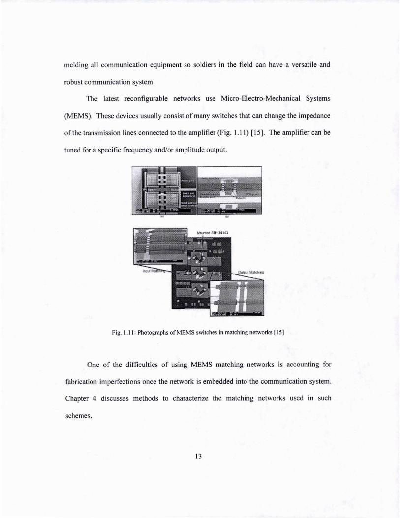
The latest reconfigurable networks use Micro-Electro-Mechanical Systems
(MEMS). These devices usually consist of many switches that can change the impedance
of the transmission lines connected to the amplifier (Fig. 1.11) [15]. The amplifier can be
tuned for a specific frequency and/or amplitude output.
Fig. 1.11 : Photographs ofMEMS switches in matching networks [15]
One of the difficulties of using MEMS matching networks is accounting for
fabrication imperfections once the network is embedded into the communication system.
Chapter 4 discusses methods to characterize the matching networks used in such
schemes.
13

1.7 Organization of Thesis
Chapter 2 discusses the application of retrodirective arrays in secure small
satellite networks. The quadruple subharmonic mixing technique has allowed array
design to account for the limited space and DC power of the satellite.
An electronically steered phased array is discussed in Chapter 3 as an alternative
to a mechanically steered satellite tracking dish for mobile applications. A one
dimensional full-duplex and two-dimensional transmit frequency-controlled phased array
is designed and demonstrated. Simple steering control is emphasized to avoid
complexities and ease integration with tracking and control systems.
Chapters 2 and 3 discussed work with the communication antenna arrays.
Reducing circuitry is important when combining communication systems. With
advances in configurable networks, circuits such as amplifiers and mixers use adaptable
adjustable networks to adjust power levels within the system. Chapter 4 introduces
methods to characterize such a system and its components.
Lastly conclusions are made. Further ideas and thoughts for futore research are
discussed in Chapter 5.
14

CHAPTER 2
RETRODIRECTIVE ANTENNA ARRAYS FOR USE IN
SMALL SATELLITE NETWORKS!
2.1 Introduction
Frqm 2003 to 2005 the University of Hawaii engineered the Hokulua (Twin Stars)
project The University of Hawaii received a $100,000 grant funded by the Air Force
Office of Scientific Research (AFOSR), and mentored by Air Force Research Lab
(AFRL), NASA, and the American Institute of Aerospace and Aeronautics (AlAA) [19-
21]. The University of Hawaii was one of 13 Universities within the United States
participating in a competitive initiative to help develop, fabricate, and launch advanced
nanosatellite systems.
Hokulua's mission was to demonstrate and test the applicability of retrodirective
array technology for satellite-to-satellite communications within distributed small-
satellite networks by designing, fabricating and testing a retrodirective link in a pair of
satellites [22]. One satellite houses the retrodirective array and the other is designed as a
transponder satellite to validate the retrodirective inIplementation.
2.2 Design Parameters
To validate a successful mission, the quality of the transmission link between the
two orbiting nanosatellites must be analyzed. The power measurements of a transmitted
I Portions of this chapterbave been published in [16], [17], [18]
15
and retroreflected continuous wave signal are recorded over a period of time. The free-
floating nature of the satellites allows both communication arrays on the satellites to
deviate from broadside. A semi-tlexible tether is used to prevent the satellites from
drifting too far away from each other, while still allowing the satellites a limited range of
motion acceptable to test the steering capabilities of the retrodirective array.
One satellite, designated as the transponder, interrogates the retrodirective
satellite and receives and measures the power of the retroretlected signal. The other
contains the retrodirective array (Fig. 2.1 and Fig. 2.2).
Receive ~----------,krum~
• Retroreflected Signal
Transponder SateDIIe
Transmit '--__________ ---'Anten~
• Interrogator Signal
RetrodlrecUve Array
Fig. 2.1: Schematic of satellite communicstion link
Fig. 2.2: Pair of experimental nanosatellites, retrodlrective satellite on the right and interrogator I receive satellite on the left
16
Retrodlrectlve SeteIIlt8
The communication system design is influenced by the physical characteristics of
the small satellite. First, the free-floating nature of the small satellites makes it necessary
to demonstrate a two-dimensional retrodirective lIITIly. Secondly. the lack of attitude
control requires circularly polarized antennas to prevent polarization mismatches due to
varying orientations of the transponder and retrodirective satellite. The designated
frequency for the satellite-to-satellite communication system is 10.5 GHz.
Chapter 1 introduced three methods for achieving retrodirectivity. The phase
conjugation technique is flexible in design. allowing circuitry to fit within the lOx lOx
15 em satellite housing. The phase conjugation circuitry typically uses heterodyne
mixers to achieve phase conjugation, Fig. 2.3 [13]. The next section discusses
heterodyne mixing and other phase conjugation methods, analyzed in further detail.
+3'1' ·3'1'
HeI8IOCIyn9 _Bleach
element
+2'1' .2q>
(a)
+1'1' ·1'1'
o o
fLO c 2fm:
(b)
Fig. 23: (a) Phase conjugating array using heterodyne mlxOl!l at each element, (b) Individual heterodyne mixer and antenna element
17
2.3 Mixing Techniqnes
The methods for achieving phase-conjugation are evaluated for the feasibility in
our proposed nanosatellite communication system. Due to the volume, power, and
budget limitations of the small satellite, different mixing techniques are evaluated, each
having their own pros and cons.
A. Fundanrental Mixing Techniqui
Analyzing nonlinear circuits and their associated UV curves is the traditional way
to describe the generation of frequencies. By applying the heterodyne mixing
components with non-linear circuit analysis in Fig. 2.4. the associated UV curve and
exponential UV characteristics can be expressed as a power series [23]:
1= aV +bV2 +cV' +dV4 +eV' ... (2.1)
where a, b, c, d, and e are constant power series coefficients. unique to specific devices.
(a)
+ V
(b)
Fig. 2.4: (a) Diode mixing circuit fed by voltage sourc:e, (b) IN characteristic of diode
If Va is the sum of both LO and RF signals,
Va = V; cos(llIw t)+ Va cos(IlIRFt + qJ)
a This section is reprinted in part from [24] with permission from the author.
18
v
(2.2)

If (2.2) is substituted back into (2.1) the first tenn results in
IQ = oV. COS{tDw/)+aVz COS{tDRFI + tp) (23)
After simplifying through trigonometric identities the second tenn becomes
If the LO frequency is set to twice the RF frequency, oow = 200RF and substituted into
(2.3) and (2.4), the sum becomes
The phase-conjugated RF signal of the second tenn in (2.2) is shown as
(2.6)
The resulting phase conjugation applies across the entire array, resulting in
retroreflection of the IF signal back towards the RF source. The higher frequency tenns
in (2.5) are undesired, non-phase-conjugated signals that are easily filtered and
suppressed due to the large difference between frequencies.
B. Subhannonic Mixing Technique
In fundamental mixing, the squared term in (2.1) is used for phase conjugation.
In subharmonic mixing, the third-order harmonic term cV3 from (2.1) is used [25], [26].
The third term from the substitution of (2.2) into (2.1) becomes:
19
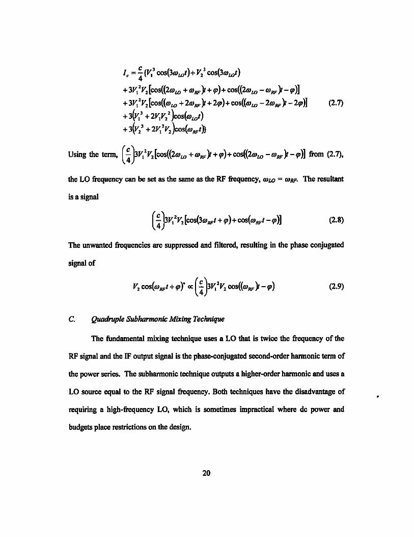
I. = *{v,l cos(3OJwt)+ V,l cos(3OJwt)
+ 3V,'V,[cos«2OJw + OJRF)t + V')+cos«2OJw -OJRF )t-V')] + 3V,'V,[cos«OJw + 2OJRF )t+ 2V')+ cos«OJw -2OJRF )t-2V')] (2.7)
+3{v,l +2V,V,'}coS(OJwt)
+ 3{v/ + 2V,2V,)coS(OJRFt)}
the LO frequency can be set as the same as the RF frequency, OJw = OJRF. The resultant
is a signal
(2.8)
The unwanted frequencies are suppressed and filtered, resulting in the phase conjugated
signal of
(2.9)
C. Quadruple Subhannonic Mixing Technique
The fundamental mixing technique uses a LO that is twice the frequency of the
RF signal and the IF output signal is the phase-conjugated second-order harmonic term of
the power series. The subharmonic technique outputs a higher-order harmonic and uses a
LO source equal to the RF signal frequency. Both techniques have the disadvantage of
requiring a high-frequency LO, which is sometimes impractical where de power and
budgets place restrictions on the design.
20
•

A quadruple subharmonic mixing approach was adopted in our system. From
(2.1), the e VS term can be extracted from the substitution of (2.2) into (2.1) as similarly
done for the b VZ and c JP in (2.4) and (2.7) respectively. The resulting term for the output
of the mixer can be described as
(2.10)
From (2.10), (O/F = 4(Ow -(ORF. To obtain (OfF = (ORF as done with the
fundamental and subharmonic mixing, the required LO frequency has to be half of the RF
frequency, (Ow = (0:; . The conjugate term becomes:
(2.11)
Anti-parallel diodes suppress the second harmonic of the LO, which is at the same
frequency of the RF and other oddoQrder mixing terms can be filtered out. The phase-
conjugating operation through the quadruple subharmonic mixing further reduces the
need for a high frequency LO source and has been adopted for use in the retrodirective
satellite.
21

2.4 Retrodirectlve Circuitry
A. Mixer A"ay Design
The RF frequency,lRF into the mixers is selected at 10.5 GHz. To distinguish
between interrogated and retroreflected signal, the IF frequency,llF is selected to be
10.45 GHz. The relationship changes between RF and IF frequencies as mentioned in
Section 2.3C. From (2.1 0), the IF and RF frequencies are substituted into
IIF = 41 LO - I RF and the LO frequency can be solved, resulting in
10.45GHz= 41LO -IO.5GHz
Solving for lro results in
lLO =5.2375GHz
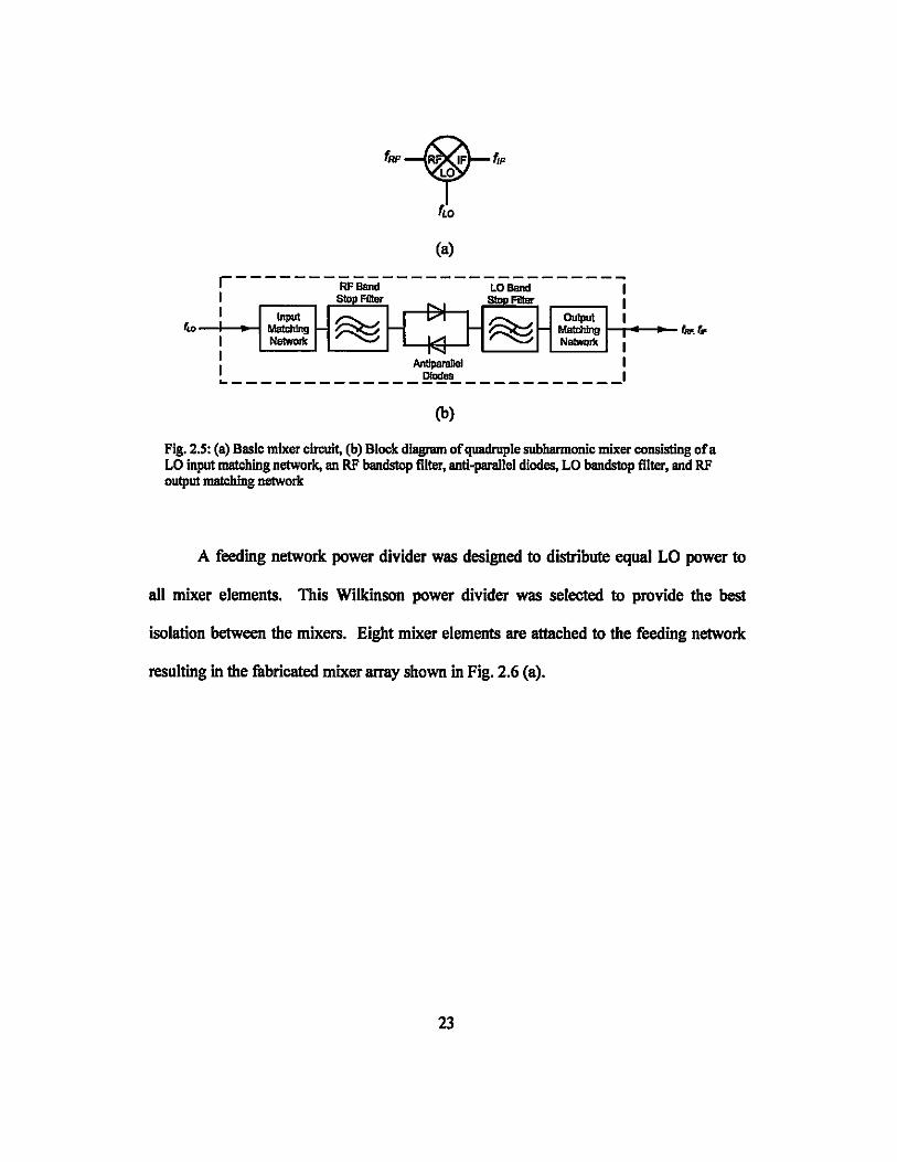
A typical mixer has three ports, one dedicated to the RF, IF and LO signals, Fig.
2.5 (a). Fig. 2.5 (b) shows a block schematic of an individual quadruple subharmonic
mixer using Agilent HMS-8202 anti-parallel diodes. The RF signal and the IF signal
share the same port. The mixer circuitry includes a RF blocking band stop filter
preventing the RF signal from reaching the LO source and a LO band stop filter blocking
leakage of the LO signal. Input and output matching networks match the impedance of
the mixer to connecting circuits and help minimize conversion loss. The microstrip
filters and matching networks are printed on Rogers TMM4 substrate (Er-4.5, h=O.038l
cm).
22
(a)
r-------~~-------LO~------I I _~ _~ I
fw : 'I=H~H : H~H=I:' · f~.~ I ~ I I DiDd8s I ----------------------------
(b)
Fig. 2.5: (a) Basic mixer circuit, (b) Block diagram of quadruple subharmonic mixer consisting ofa LO input matching network, an RF bandstop filter, anti-parallel diodes, LO bandstop filter, and RF output matching network
A feeding network power divider was designed to distribute equal LO power to
all mixer elements. This Wilkinson power divider was selected to provide the best
isolation between the mixers. Eight mixer elements are attached to the feeding network
resulting in the fabricated mixer array shown in Fig. 2.6 (a).
23
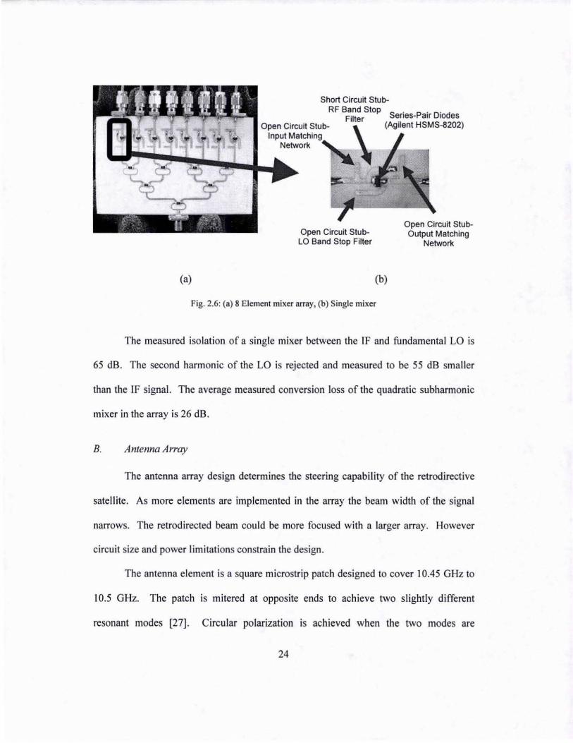
(a)
Open Circuit StubLO Band Stop Filter
(b)
Fig. 2.6: (a) 8 Element mixer array, (b) Single mixer
Open Circuit StubOutput Matching
Network
The measured iso lation of a single mixer between the IF and fundamental LO is
65 dB. The second harmonic of the LO is rejected and measured to be 55 dB smaller
than the iF signal. The average measured convers ion loss of the quadratic subharmonic
mixer in the array is 26 dB.
B. Antenna Array
The antenna array design determines the steering capability of the retrodirective
satellite. As more elements are implemented in the array the beam width of the signa l
narrows. The retrodirected beam could be more focused with a larger array. However
circuit size and power limitations constrain the design .
The antenna element is a square microstrip patch designed to cover 10.45 GHz to
10.5 GHz. The patch is mitered at opposite ends to achieve two slightly different
resonant modes [27]. Circular polarization is achieved when the two modes are
24

orthogonal to each other and 90· out of phase (Fig. 2.7). The antenna is fabricated on
Rogers TMM3 substrate (Er=3.27, h=O.0635 cm).
L
wI -;:--m-r -I ...J
w1
Fig. 2.7: Patch antenna element with dimensions L = 0.762 em, c = 0.102 em, wi = 0.0457 em, I = 0.541 em, w2 = 0.150 em.
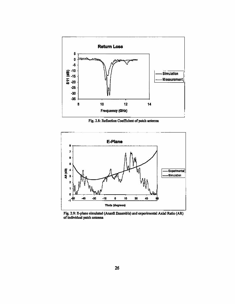
The return loss of a single patch is shown in Fig. 2.8. The axial ratio (AR) is the
ratio of co-polar and cross-polarization in a one-dimensional plane. Ideally the AR
should be relatively the same for both E and H planes of the antenna. The simulated and
measured AR is shown in Fig. 2.9 and Fig. 2.10 both E and H planes respectively. The
discrepancies between measured and simulation values depicted in the AR patterns are a
result of the reflective environment the antennas were tested in. The sensitive nature of
the axial ratio test requires test conditions obtainable in an anechoic chamber.
25
RetumL088
5
0 -""" -5 't( v
iii -10 ~-15
-Simulation - -Measurement C;; -20
-25
-30 -35
8 10 12 14
Frequency (GHz)
Fig. 2.8: Reflection Coefficient ofpatclt antenna
E.Plana 8
7
8
8
/!4 1-Experlmentall !1i 3 -Simulation
2
0
-I 0 18 30 4S
Tbe1B (des",e.)
FIg. 2.9: E-plane simulated (Ansoft Ensemble) and experimental AxIal Ratio (AR) of individual patcb antenna
26
H-Plane 9r------------------------------, 8
7
8
is ~4
3
2
-60 -45 -30 ·16 o 16 30 45 80
Th.ta (d.g .... )
I--ExperlmenlaJ I -SlmuJatlon
Fig. 2.10: H-plane simulated (Ansoft Ensemble) and experimen1al AR of individual patch antenna
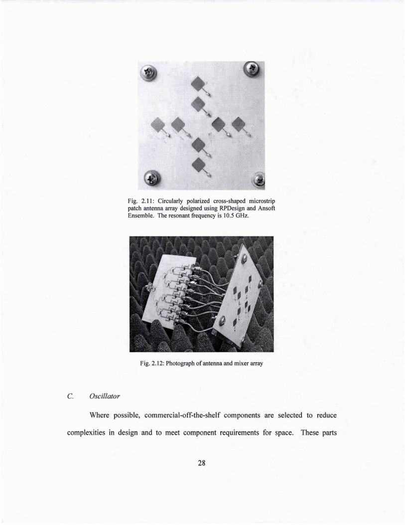
Significant rettodirectivity requires an array of at least four elements per
dimension. Conventionally, this is achieved with a 4 x 4 array layout. To reduce circuit
size and required feed power, a cross-shaped array consisting of four elements in two
orthogonal dimensions was used instead, reducing the amount of elements from 16 for
the conventional array to eight elements. The array spacing is 0.484)" = 1.383 cm
between elements (Fig. 2.1 I). With this configuration the array should be able to exhibit
retrodirectivity in any direction. The antenna array is attached to mixer array depicted in
Fig. 2.12.
27
C. Oscillator
Fig. 2.11: Circularly polarized cross-shaped microstrip patch antenna array designed using RPDesign and Ansoft Ensemble. The resonant frequency is 10.5 GHz.
Fig. 2.12: Photograph of antenna and mixer array
Where possible, commercial-off-the-shelf components are selected to reduce
complexities in design and to meet component requirements for space. These parts
28
include the local oscillator for both interrogator and retrodirective systems and various
connectors.
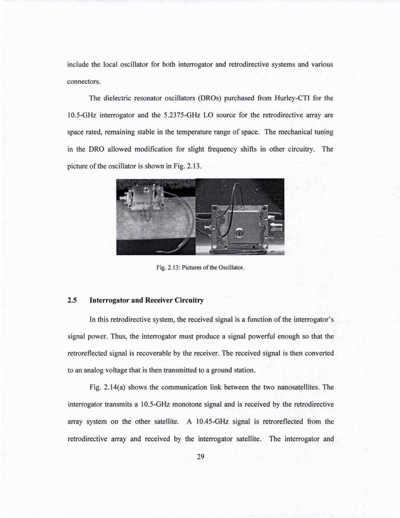
The dielectric resonator oscillators (DROs) purchased from Hurley-CTI for the
IO.5-GHz interrogator and the 5.2375-GHz LO source for the retrodirective array are
space rated, remaining stable in the temperature range of space. The mechanical tuning
in the DRO allowed modification for slight frequency shifts in other circuitry. The
picture of the oscillator is shown in Fig. 2.13.
Fig. 2.1 3: Pictures of the Oscillator.
2.S Interrogator and Receiver Circuitry
In this retrodirective system, the received signal is a function of the interrogator' s
signal power. Thus, the interrogator must produce a signal powerful enough so that the
retroreflected signal is recoverable by the receiver. The received signal is then converted
to an analog voltage that is then transmitted to a ground station.
Fig. 2.14(a) shows the communication link between the two nanosatellites. The
interrogator transmits a JO.5-GHz monotone signal and is received by the retrodirective
array system on the other satellite. A I0.45-GHz signal is retroreflected from the
retrodirective array and received by the interrogator satellite. The interrogator and
29
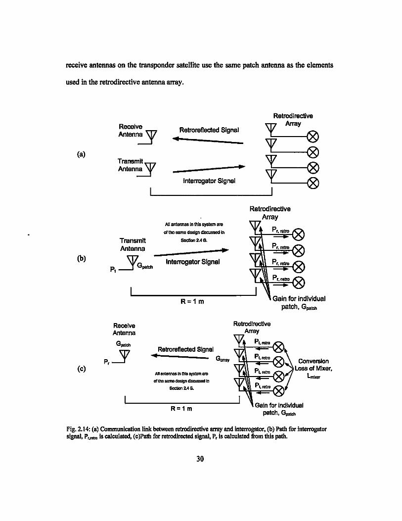
receive antennas on the transponder satellite use the same patch antenna as the elements
used in the retrodirective antenna array.
(a)
(b)
(c)
Retrodlrectlve Array Receive \f Antenn~
Retroreflected Signal
® .. \f ®
Trens~ 'E ® Antenna ~
Interrogator Signal '[ ®
Transmit Antenna
p,3GpaIdI
Receive Antenna
G_
p,-.Y
AD antennas In IhIs system are
01 the ...... cI8sIgn dIsc:ussed ..
_2.49.
~
Interrogator Signal
R=1m
Retroreflected Signal .. Garro.
AD antennas In this 8)'8tBm 81'8
01 the same design discussed In
_2.48.
R=1m
Retrodlrective Array
Gain for Individual patch, GpalCh
Retrodlrectlv8 Array
....!::JhF'-OO, ... \ Conversion Loss of Mixer,
lmi....
Gain for IndMdual patch,G_
Fig. 2.14: (a) Communication link between retrodirective array and interrogator, (b) Path for interrogator signal, P,_ is calculated, (c)Patb for retrodIrected signal, P, is calculated from this path.
30

Although the differences in transmit and receive frequencies are not essential to
the retrodirectivity process, it does allow one to distinguish between the two signals in
the laboratory. The returned signal at 10.45 GHz must be strong enough after
downconversion to be detected. The power received by the interrogator can be calculated
by following the path of the signal from the interrogator antenna (Fig. 2.14). PI is the
output power of the interrogator source, G.,.,.i, is the gain of the patch antennas, Luux.r is
the conversion loss of the phase-conjugating mixer, and Garray is the gain of the phase-
conjugating array. Using the Friis transmission formula, the power received at each
element in the retrodirective array (Fig. 2.l4(b» is
P,,..,,. = (_1_2 )P,G przI<h (~G przI<h) '4HR 4"
(2.12)
The power transmitted by the retrodirective array is affected by the individual mixer
conversion loss and the results in
The power received at the receiver antenna is dependent on the power transmitted by the
retrodirective array (Fig. 2.14( c», and the gain of the receiving patch element is given by
P, = (_I 2 )P,.-. 'Garray 1MllI( ;} G przI<h) 4HR - 4"
(2.14)
The gain of the retrodirective array, G array _1MllI is dependent on the gain of the individual
patch antenna elements, G przI<h and the gain associated with the array factor (AF), G an'Q)I
results in
31
Simplifying (2.15) gives
The interrogator oscillator output, the frequency, communication distance,
conversion loss of the mixers, patch antenna gain, and array gain are all known
parameters, which allow us to find the actual received power by the interrogator front end
about -100 dBm. The minimum detectable power for the detector is -60 dBm. Therefore
the receiver circuit should be designed so that it can provide 40 dB gain. The system
schematic is shown in Fig. 2.15.
50 MHz Detector
Downconvertlng Mixer
50 MHz Amplifier
LNA LNA Tx
10.5GHz ~ W OscIllator~
10.45 GHz 4
10.5GHz
I_ Received Signal B Interrogator Signal I
Fig. 2.15: Schematic of ReceIver circuitry. Inteiiogator tnmsmIts 10.5 GHz signal (Tx). Receiver mixes 10.45 and 10.5 GHz (Rx) and produces 8
downconverted signal at SO MHz.
To conserve dc power, space, and other limited resources aboard the 1500-cubic-
em nanosatellite, a separate local oscillator (LO) for the receiver was eliminated from the
32

design. As mentioned in Section 2.4 A, typical mixers have dedicated LO ports. Instead,
the mixer is designed with the RF signal and IF signal sharing the same port. The LO
signal for the receiver is coupled off from the interrogator via the patch antennas of the
interrogator and receiver. This antenna-coupling scheme eliminates the need for a power
divider. The distance between the antennas is optimized so that the LO power for the
mixer is 0 dBm after a two-stage amplifier. The mixing of the two signals produces a 50-
MHz downconverted signal. Because a diOde mixer is used, an amplifer following the
mixer compensates for conversion losss. Based on the link budget, a prototype system
was fabricated using commercial-off-the shelf parts. Components in the
interrogator/receiver were carefully chosen based on constraints such as size, weight,
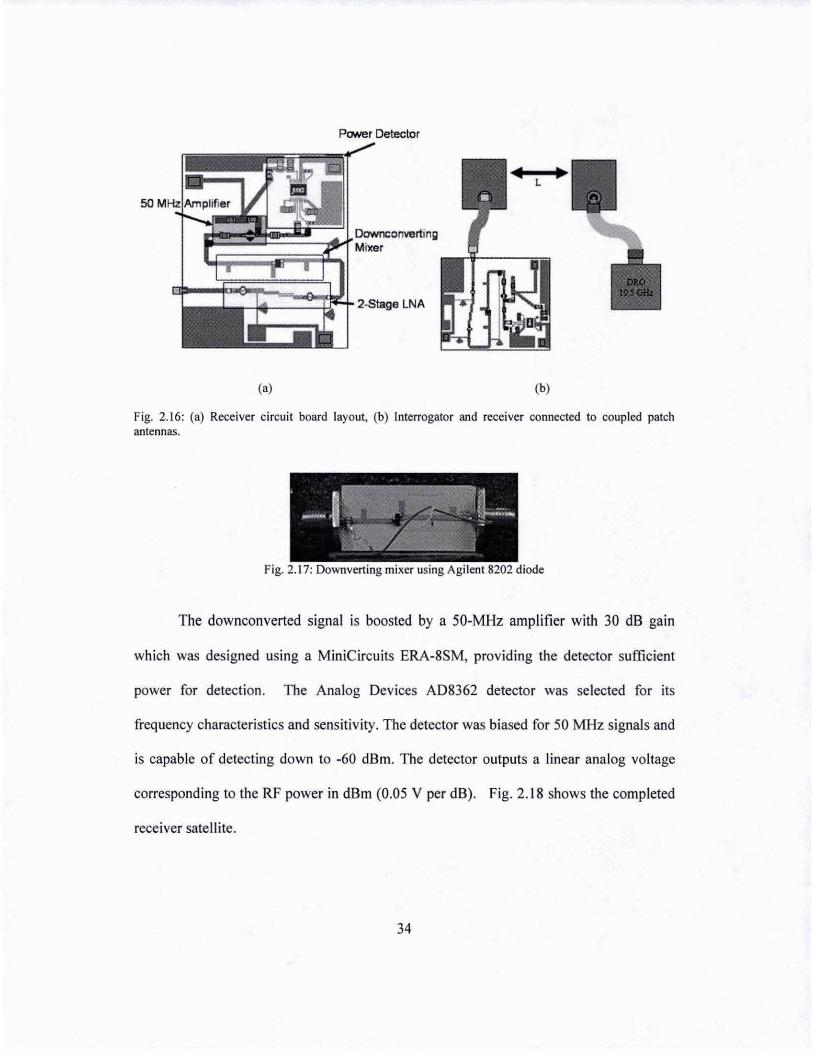
cost, and reliability. Fig. 2.16(a) shows the single-board design consisting ofa two stage
amplifier circuit, downconverting mixer, 50-MHz amplifier, and the power detector. The
receiver circuitry is then connected to the corresponding antennas. A two-stage amplifier
was designed using internally matched Agilent MGA 86576 LNAs to amplify the
retrodirected signal and coupled LO power by 17 dB.
The mixer was designed using an Agilent 8202 Schottky diode (Fig. 2.17),
resulting in a 10 dB conversion loss. The optimal LO power into the mixer is
approximately 0 dBm. To achieve this, the distance L between the receiver and
interrogating antennas was calibrated (Fig. 2.16(b».
33
PaNer Detector
50 Ml-izlAl"plifier
Mixer
i::E~f~~~~4 2-Stage LNA
(a) (b)
Fig. 2.16: (a) Receiver circuit board layout, (b) Interrogator and receiver connected to coupled patch antennas.
Fig. 2.1 7: DOWDverting mixer using Agilen! 8202 diode
The downconverted signal is boosted by a 50-MHz amplifier with 30 dB gain
which was designed using a MiniCircuits ERA-SSM, providing the detector suflicient
power for detection. The Analog Devices ADS362 detector was selected for its
frequency characteristics and sensitivity. The detector was biased for 50 MHz signals and
is capable of detecting down to -60 dBm. The detector outputs a linear analog voltage
corresponding to the RF power in dBm (0.05 V per dB). Fig. 2.IS shows the completed
receiver satellite.
34
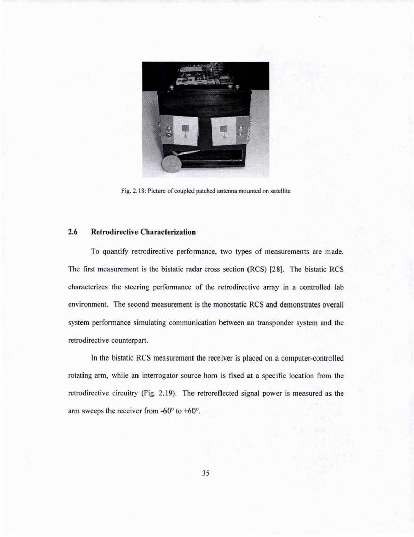
fig. 2. 18: Picture of coupled patched antenna mounted on satellite
2.6 Retrodirective Characterization
To quantitY retrodirective performance, two types of measurements are made.
The first measurement is the bistatic radar cross section (RCS) [28] . The bistatic ReS
characterizes the steering performance of the retrodirective array in a controlled lab
environment. The second measurement is the monostatic ReS and demonstrates overall
system performance simulating communication between an transponder system and the
retrodirective counterpart.
In the bistatic ReS measurement the receiver is placed on a computer-controlled
rotating arm, while an interrogator source horn is fixed at a specific location from the
retrodirective circuitry (Fig . 2.19). The retroreflected signal power is measured as the
arm sweeps the receiver from _600 to +600•
35
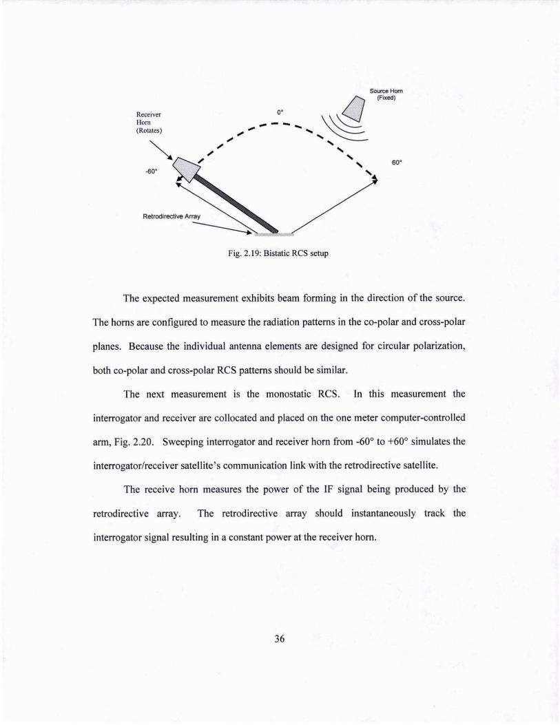
Receiver Hom (Rotates)
-60·
Retrodirective Array
~ Fig. 2.19: Bistatic Re S setup
The expected measurement exhibits beam forming in the direction of the source.
The horns are configured to measure the radiation patterns in the co-polar and cross-polar
planes. Because the individual antenna elements are designed for circular polarization,
both co-polar and cross-polar RCS patterns should be similar.
The next measurement is the monostatic RCS. In this measurement the
interrogator and receiver are collocated and placed on the one meter computer-controlled
arm, Fig. 2.20. Sweeping interrogator and receiver horn from -600 to +600 simulates the
interrogator/receiver satellite 's communication link with the retrodirective satellite.
The receive horn measures the power of the IF signal being produced by the
retrodirective array. The retrodirective array should instantaneously track the
interrogator signal resulting in a constant power at the receiver horn.
36
o· 60·
-C),. ----+--u sourc~" (:] Hom
Receive Hom
2.7 Experimental Results
Retrodireclive array
Fig. 2.20: Monostatic ReS setup
60·
The hardware was tested in a methodical manner. The first step in the testing
procedure involves measuring the performance of the retrodirective array before
installation in the satellite bus. Two-dimensional steering is confirmed and demonstrated
in Section 2.7.1.
The second part of the procedure, Section 2.7.2, the retrodirective hardware has
been integrated into the satellite bus. Onboard processors control the retrodirective array
and the system is tested once again before communicating with the transponder satellite.
After confirmation the retrodirective circuitry is properly working, the communication
link is established between the two satellites. The received power of the communication
37
link is measured over a predetermined period of time. The data is recorded and
transferred from the transponder satellite to the ground station.
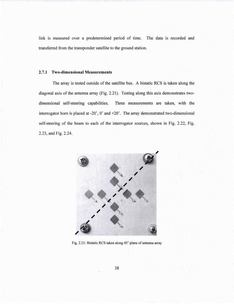
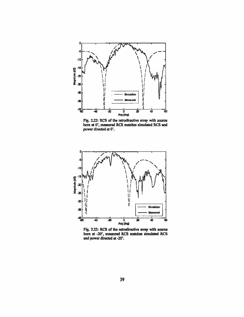
2.7.. Two-dimensional Measurements
The array is tested outside of the satellite bus. A bistatic ReS is taken along the
diagonal axis of the antenna array (Fig. 2.21). Testing along this axis demonstrates two-
dimensional self-steering capabilities. Three measurements are taken, with the
interrogator horn is placed at -20 ' ,0' and +20' . The array demonstrated two-dimensional
self-steering of the beam to each of the interrogator sources, shown in Fig. 2.22, Fig.
2.23, and Fig. 2.24.
~ ,," ~ ,,"
~~",,~~~ " " "
Fig. 2.21: Bistatic ReS taken along 45' plane of antenna array
38
·10
.3:)
~~--~~-L~~~--~o--~~~L-~~~~m An1J Ida;)
0
-5
·10
0
-5
• I-:;!) :iL25
-:'10
-:is
-4IJD
I I \ I \
\ f \ \ I \I \ I \1 \ I \1 \ I \1 \, ( 1==1 'I
~ -4D -:;!) 0 :;!) 40 60
AnlI (deg)
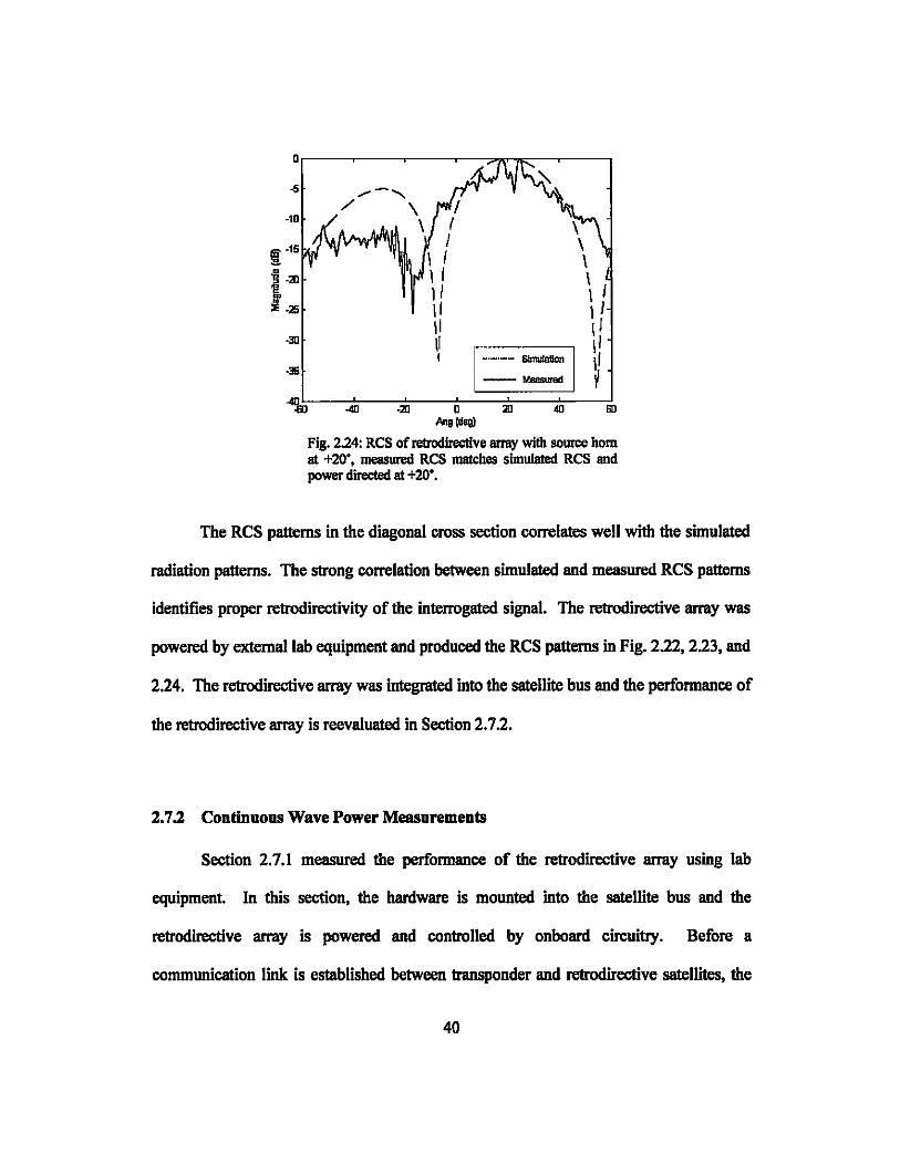
Fig. 2.24: RCS ofretrodirective array with source born at +20'. measured RCS matches simulated RCS and power directed at +20'.
The RCS patterns in the diagonal cross section correlates well with the simulated
radiation patterns. The strong correlation between simulated and measured RCS patterns
identifies proper retrodirectivity of the interrogated signal. The retrodirective array was
powered by extema1lab equipment and produced the RCS patterns in Fig. 2.22, 2.23, and
2.24. The retrodirective array was integrated into the satellite bus and the performance of
the retrodirective array is reevaluated in Section 2.7.2.
2.7.2 Continuous Wave Power Measorements
Section 2.7.1 measured the performance of the retrodirective array using lab
equipment. In this section, the hardware is mounted into the satellite bus and the
retrodirective array is powered and controlled by onboard circuitry. Before a
communication link is established between transponder and retrodirective satellites, the
40
retrodirective satellite is individually tested by taking bistatic and monostatic Res
measurements.
A. Bistatic Measurements
The measurements presented are the bistatic ReS of the retrodirective array
integrated into the satellite bus. This section's measurements differ from section 2.7.1
measurements because the retrodirective array is powered and controlled from the
satellite bus and not manually powered by lab equipment. The first ReS measurement
uses a hom antenna as a source and is fixed at broadside, 00• The power is measured by
the sweeping receive hom and is centered at 00 Fig. 2.25. In the second and third
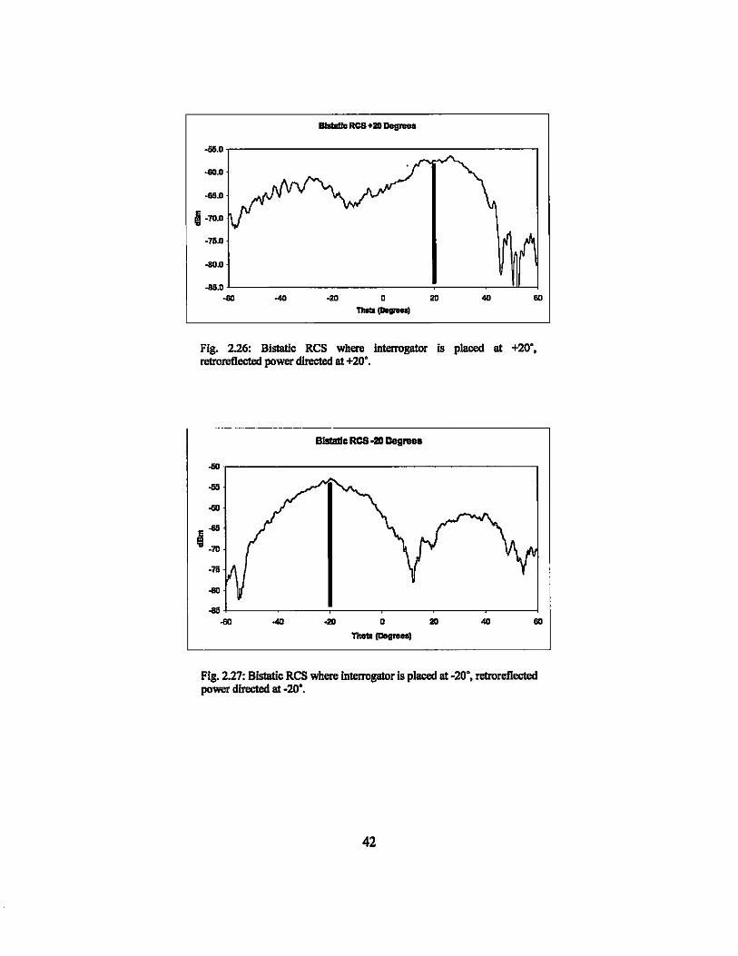
measurements, the source hom was placed at +200 and -200• In both cases the peak
power was located at the source angle Fig. 2.26 and 2.27.
B_ RCS 0 Degrees
~r---------------~=------------------.
...
-78
... ~--~------------~--------~~----~ ... -211 D 2D .. 'IhoII (Dogrooa)
Fig. 2.25: Blstatlc RCS where InleuogatOJ is placed at 0', retroreflected power directed at 0'
41
_RC8+2DDegnIea
..s5.0,----------------------,
..... 0
... .0
1-70.0
-76.D
.... .0
-4111.0 +-___ ---_--_----';..---_-...!.JI.---l .... ·20 0 20 4D an ..--Fig. 2.26: Bislatic RCS where interrogator is placed at +20', reIrorefiected pcwer directed at +20'.
_. RCS -20 De_ .... ,----------------------,
-76
....
... +---_---T---_---_--_--~ .... 60
Fig. 2.27: Bislatic RCS where Interrogator is placed at -20', retroreflected pcwer directed at -20'.
42

The bistatic ReS patterns demonstrate the retrodirective array in the satellite bus
properly steers the beam to the interrogator source. The graphs show the difference
between the main and side lobes of 10 dBm.
B. Monostotic Measurements
Fig. 2.28 depicts the monostatic Res. Two hom antennas for the interrogator
source and receiver simulate the transmit and receive antennas on the transponder
satellite. The range in which a detectable retrodirected signal is received is shown by the
vertical lines on the graph from -40' to +40'. Fig. 2.29 shows the monostatic ReS
pattern of a fixed array without retrodirective circuitry. When compared to the
retrodirective monostatic pattern, it is observed that the range in which maximum power
of the IF signal is detected increases by four.
Fig. 2.28: Monos1atic RCS of the retrodirective array, retrodirective array demonstrates steering range of -40" to 40".
43
~.------------.--~~-------------,
...
...
'"
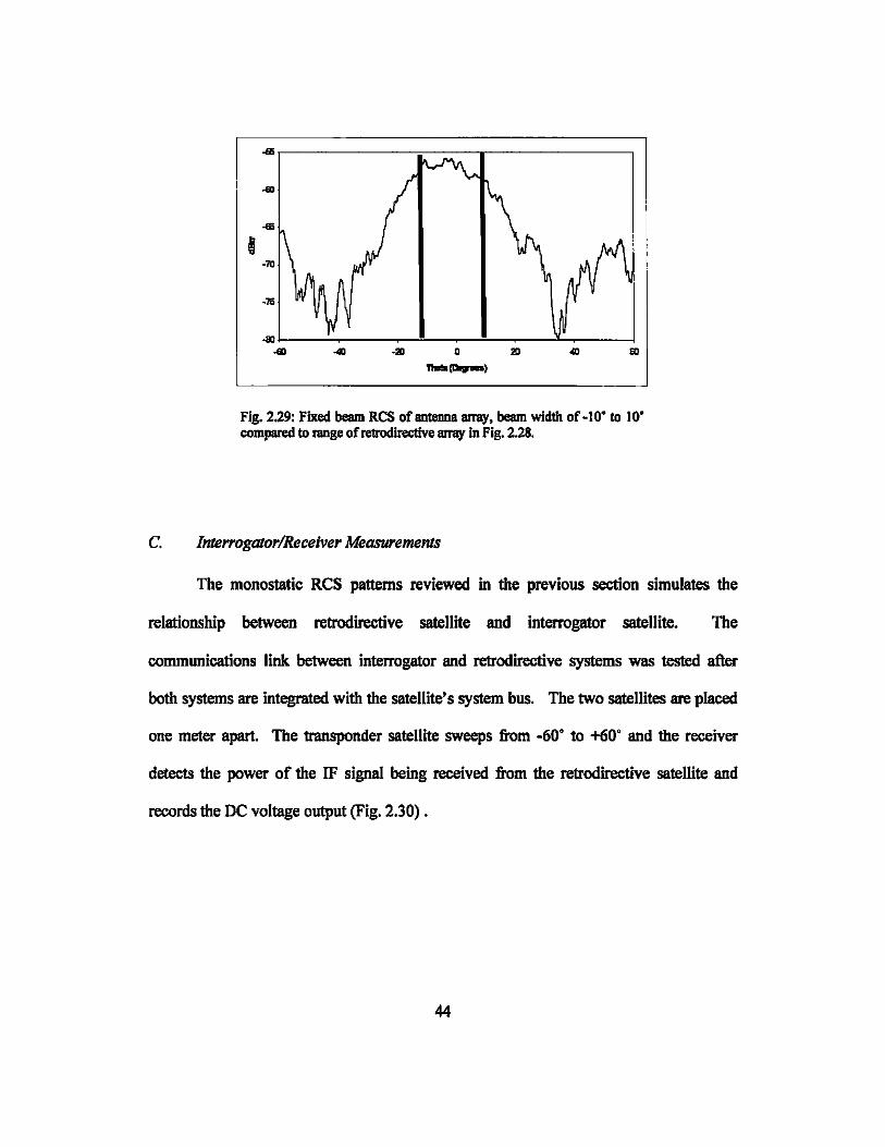
Fig. 2.29: Fixed beam RCS of antenna array, beam width of -10· to 10· compared to range of retrodirectlve array in Fig. 2.28.
c. Inte"ogalorlReceiver Measurements
The monostatic ReS patterns reviewed in the previous section simulates the
relationship between retrodirective satellite and interrogator satellite. The
communications link between interrogator and retrodirective systems was tested after
both systems are integrated with the satellite's system bus. The two satellites are placed
one meter apart. The transponder satellite sweeps from -60· to +60· and the receiver
detects the power of the IF signal being received from the retrodirective satellite and
records the DC voltage output (Fig. 2.30) .
44
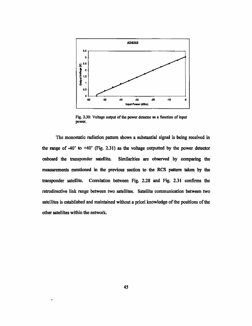
AD838Z
~6.---------------------------------,
3
2: 2.6
f ,.: f '
0.5
.~~------------------~--------~ ... ·50 ... .,. • IftJAII Pern, edBm)
Fig. 2.30: Voltage output of the power detector as a function of input power.
The monostatic radiation pattern shows a substantial signal is being received in
the range of -40' to +40' (Fig. 2.31) as the voltage outputted by the power detector
onboard the transponder satellite. Similarities are observed by comparing the
measurements mentioned in the previous section to the Res pattern taken by the
transponder satellite. Correlation between Fig. 2.28 and Fig. 2.31 confirms the
retrodirective link range between two satellites. Satellite communication between two
satellites is established and maintained without a priori knowledge of the positions of the
other satellites within the network.
45
~.
Q8
:!: Q7
f ~8
I> ::
~3
~2
Q1
Monoatatlc RCS using d_, output
.~--------------------------------~ ... .... ... • 2D .. so 11uo1a(de_
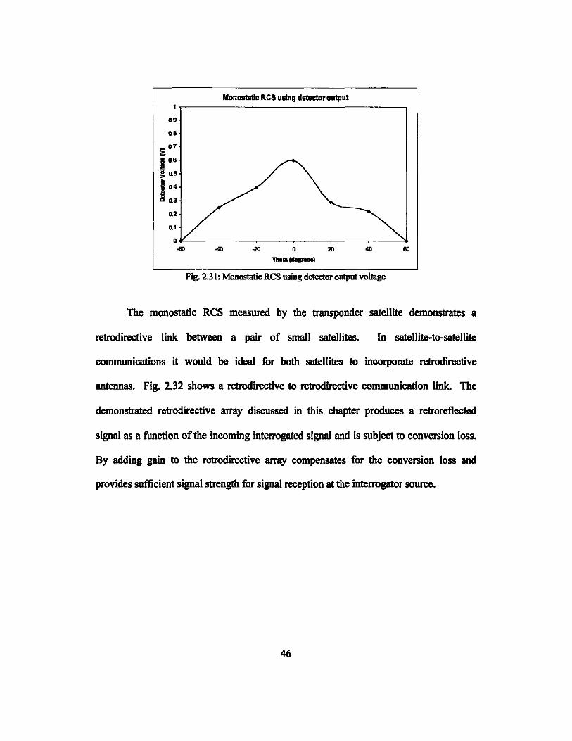
Fig. 2.31: Monos1atic RCS using detector output voltage
The monostatic ReS measured by the transponder satellite demonstrates a
retrodirective link between a pair of small satellites. In satellite-to-satellite
communications it would be ideal for both satellites to incorporate retrodirective
antennas. Fig. 2.32 shows a retrodirective to retrodirective communication link. The
demonstrated retrodirective array discussed in this chapter produces a retroreflected
signal as a function of the incoming interrogated signal and is subject to conversion loss.
By adding gain to the retrodirective array compensates for the conversion loss and
provides sufficient signal strength for signal reception at the interrogator source.
46
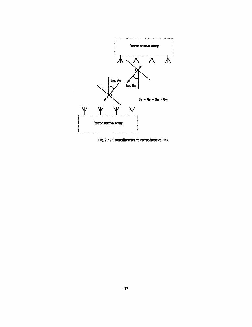
·------·-·----i Retradlrecllve Amrt ,
'···l--·I-----I--IJ
Retrcdlreclivo Amrt
Fig. 2.32: Retrodlrective to retrodlrective link
47

CHAPTER 3
FREQUENCY-CONTROLLED PHASED ARRAYS3
3.1 Introduction
The frequency-controlled array introduced in Section 1.2C expands on the
frequency-scanned array design by using heterodyne mixing at each element to keep a
constant transmit and receive frequency (Fig. 3.1). The frequency-controlled phased
array provides many desirable beam steering characteristics of conventional arrays
without complex circuitry and the high cost associated with phase shifters. The simple
control of the frequency-controlled array allows for easy integration with current systems.
A perfect application of the frequency-controlled array is integration with the M2C2
Humvee which uses GPS. The GPS system provides precise tracking of the target
communication satellite and provides accurate steering of satellite dish/antenna. The
frequency-controlled phased array steers in real time addressing the limited tracking
speed of a mechanical driven satellite dish.
, Portions ofthls chapter have been published In [291
48
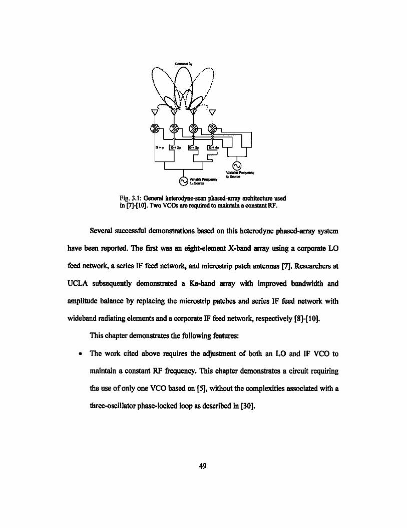
Fig. 3.1: General heteroclyne-scan phased-array architecture used in [7]-[10]. Two veOs are required to maintain 8 cons1antRF.
Several successful demonstrations based on this heterodyne phased-1IITIlY system
have been reported. The first was an eight-element X-band array using a corporate LO
feed network, a series IF feed network, and microstrip patch antennas [7]. Researchers at
UCLA subsequently demonstrated a Ka-band array with improved bandwidth and
amplitude balance by replacing the microstrip patches and series IF feed network with
wideband radiating elements and a corporate IF feed network, respectively [8]-[10].
This chapter demonstrates the following features:
• The work cited above requires the adjustment of both an LO and IF YCO to
maintain a constant RF frequency. This chapter demonstrates a circuit requiring
the use of only one YCO based on [5], without the complexities associated with a
three-oscillator phase-locked loop as described in [30].
49

• Previously reported heterodyne phased arrays operated in transmit mode only.
This chapter presents a transmit/receive array that can operate in full-duplex
mode.
• The LO corporate feed network in Fig. 3.1 can become quite unwieldy for large
arrays. This chapter demonstrates a novel series-feed network that is more
compact than a corporate feed. The design allows each mixer to be pumped with
an equal level of LO power, resulting in less than 3-dB amplitude variation over
the steering range.
3.2 One-Dimensional Full-Duplex, Voltage-Controlled Phased Array
3.2.1 Design Parameters
Fig. 3.2 illustrates the system proposed in this chapter that differs from Fig. 3.1 in
several respects. First of all, there are two sets of arrays: one four-element array for
transmission, and a second array for reception, allowing full-duplex operation. Secondly,
it is unnecessary to adjust both an LO and IF source to maintain a constant RF. In our
architecture, the second VCO is replaced by a fixed-frequency source operating at fRF.
The only expense is the additional mixer A, but it is less expensive than a VCO - a small
price for having the steering control based solely on the tuning voltage of a single VCO.
Connected to Mixers A are fixed-frequency oscillators that oscillate at fRF. The output of
Mixers A is thus fRF"fLO. This intermediate frequency signal is then routed to the mixer
array, whereupon they are mixed with fLO, resulting in fRF appearing at the antenna
elements.
50
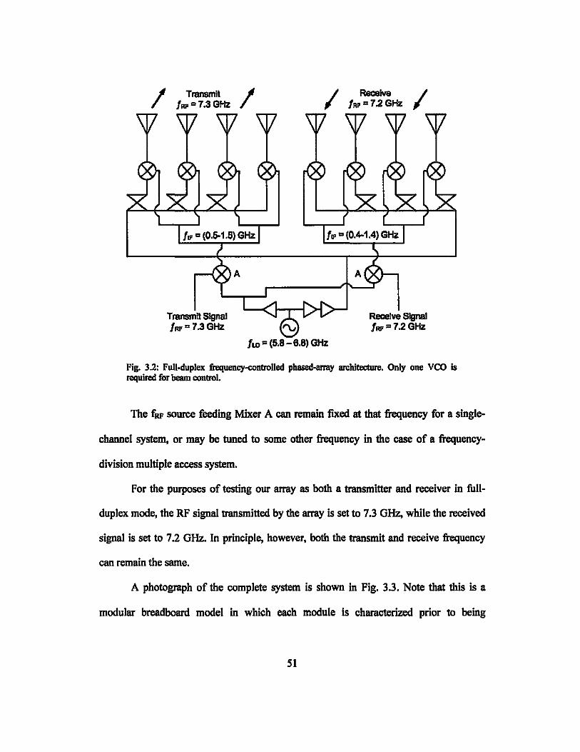
/ Transmit IfV' = 7.3 GHz / I I
fLO = (5.8 - 6.8) GHz
Fig. 3.2: Full-duplex frequency-controlled phased-array an:bitecture. Only one veo is required for beam control.
The fRF source feeding Mixer A can remain fixed at that frequency for a single-
channel system, or may be tuned to some other frequency in the case of a frequency-
division multiple access system.
For the purposes of testing our array as both a transmitter and receiver in full
duplex mode, the RF signal transmitted by the array is set to 7.3 GHz, while the received
signal is set to 7.2 GHz. In principle, however, both the transmit and receive frequency
can remain the same.
A photograph of the complete system is shown in Fig. 3.3. Note that this is a
modular breadboard model in which each module is characterized prior to being
51
integrated with each other. In a real system, there would not be SMA interconnects
between modules.
3.2.2 One-Dimensional Frequency-Controlled Circuitry and Design
A. Antenna and Mixer Arrays
The radiating-edge-fed patch antennas in Fig. 3.3 are fabricated on RT/duroid
5880 substrate (thickness 0.7874 mm, Er = 2.2). The antennas are connected to Hittite
HMC220MS8 mixers with operating RF/LO frequencies ranging from 5-12 GHz, and an
IF frequency range of DC-4 GHz. As shown in Figs. 3.2 and 3.3, the mixers are
connected through vias to rF corporate feed networks using Wilkinson power dividers.
The feed networks and mixer arrays are fabricated on RT/duroid 60 I 0.2LM substrate
(thickness 0.635 mm, Er = 10.2).
Fig. 3.3: Transmit and receive phased array. Vias connect to the veo and transmit/receive reed networks.
52

B. Phase-Delay LO Feed Network
The most straightforward way of implementing a phase-delay La feed network is
to use transmission lines of differing lengths. Fig. 3.1 shows a typical network of this
type, in which adjacent lines have successive phase sh ifts with ~=2n1l for broadside
radiation at the veo's center frequency. The disadvantage of such networks is that it
takes up considerable space, and the longer line lengths result in higher loss, resulting in
amplitude variations across the steering range. This is the type of network that was used
in [3)-[5) .
An alternative delay network is the one in [2), which consists of one transmission
line with coupled-line taps to each mixer. In that paper, each coupled-line section has the
same amount of coupling, leading to an unequal mixer conversion loss for each element.
The phase-delay La feed network proposed here is also series fed, but unlike the taps •
used in [2), successive branch line couplers are designed to tap off a varying amount of
power, resulting in an even distribution of La power to each mixer in the array.
G. Shiroma, co-member of this project, designed the phase-delay La network.
Fig. 3.4 shows the fabricated four-element phase-delay La feed network with a
progressive phase shift of ~ = 411 at 6.3 GHz.
For a lossless network, there would be a 6-dB insertion loss at each of the four
ports. Fig. 3.5 shows that between 5.8-6.8 GHz, the measured insertion loss at each port
is 8 ± 2.5 dB. The imbalance between ports is remedied by applying sufficient La power
to ensure that the mixers receive the minimum required power, while assuming a worst
case La network loss of 10.5 dB. Applying more than the minimum La power to the
mixers results in only a minimum change in mixer performance.
53
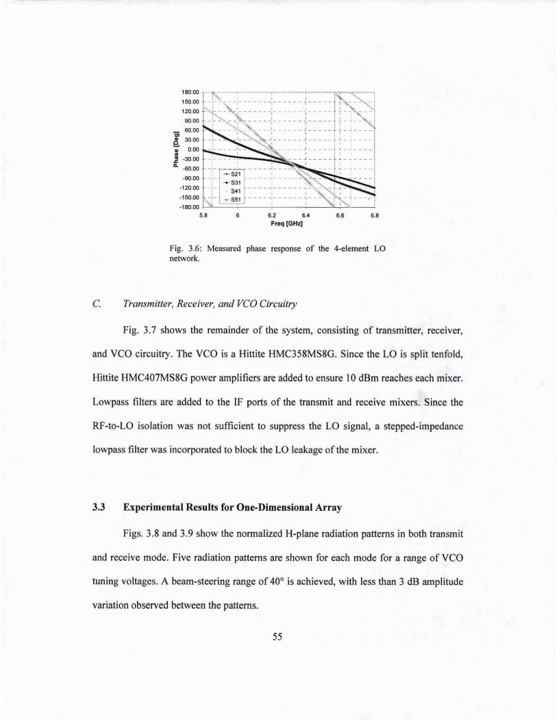
The measured phase response of the LO feed network is shown in Fig. 3.6. As
expected, the phases of the four ports are equal at the center frequency of 6.3 GHz. At
other frequencies, the progressive 4n delay lines create the phase progression required for
beam steering.
Fig. 3.4: Four-element LO reed network with a progressive phase delay of ~ = 4n. The network is fabricated on RT/duroid 60 10.2LM substrate (thickness 0.635 mm, Er = 10.2).
I"' ----,--- r----, ~ ___ L ___ ' ___ ~ ___ L __ _
, " ,. I
. 16 --~---,------~---1------- ---,
. 18 - - -1- - - ... - - -,.. - - -,- - - .. - - - .. - - -1- - -"1
." +---<---_-+------+--+--f-~ 5.8 5.9 6 6. 1 6.2 6.3 6.01 6.5 6.6 6.7 6.8
Freq [GHz]
Fig. 3.5: Measured insertion loss of the four-element LO feed network.
54
180.00
150.00
120.00
90.00
0; 60.00
• 30.00 B
-150.00 .,,-1- -- 551 ----,------,-
-180.00 5.8 • 6.2 6.4 6.6 6.8
Freq (GHZ)
Fig. 3.6: Measured phase response of the 4-element LO network.
C. Transmitter, Receiver, and VCO Circuitry
Fig. 3.7 shows the remainder of the system, consisting of transmitter, receiver,
and VCO circuitry. The VCO is a Hittite HMC358MS8G. Since the LO is split tenfold,
Hittite HMC407MS8G power amplifiers are added to ensure 10 dBm reaches each mixer.
Lowpass filters are added to the IF ports of the transmit and receive mixers . Since the
RF-to-LO isolation was not sufficient to suppress the LO signal, a stepped-impedance
low pass filter was incorporated to block the La leakage of the mixer.
3.3 Experimental Results for One-Dimensional Array
Figs. 3.8 and 3.9 show the normalized H-plane radiation patterns in both transmit
and receive mode. Five radiation patterns are shown for each mode for a range of VCO
tuning voltages. A beam-steering range of 40° is achieved, with less than 3 dB amplitude
variation observed between the patterns.
55
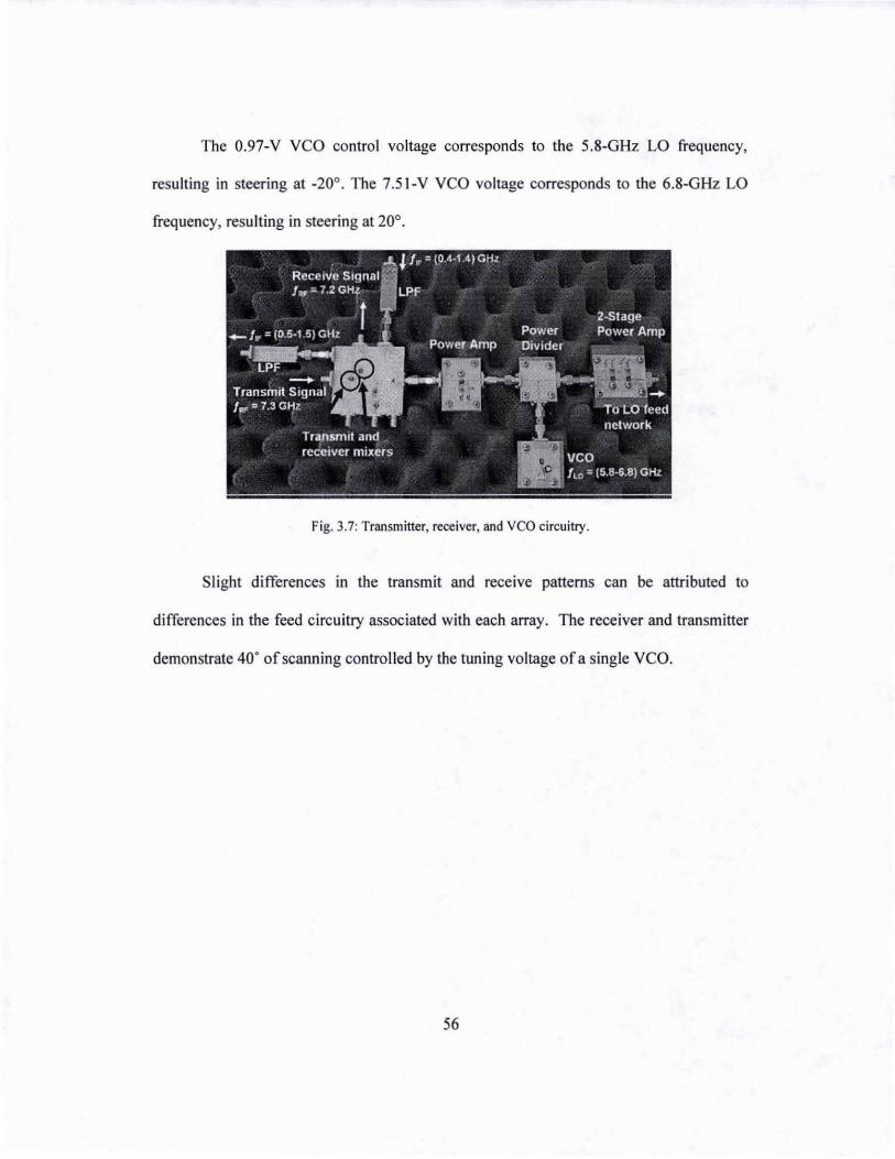
The 0.97-y yeO control voltage corresponds to the 5.8-0Hz LO frequency,
resulting in steering at _20°. The 7.51-Y yeO voltage corresponds to the 6.8-0Hz LO
frequency, resulting in steering at 20°.
Fig. 3.7: Transmitter, receiver, and yeO circuitry.
Slight differences in the transmit and receive patterns can be attributed to
differences in the feed circuitry associated with each array. The receiver and transmitter
demonstrate 40· of scanning controlled by the tuning voltage of a single yeo.
56
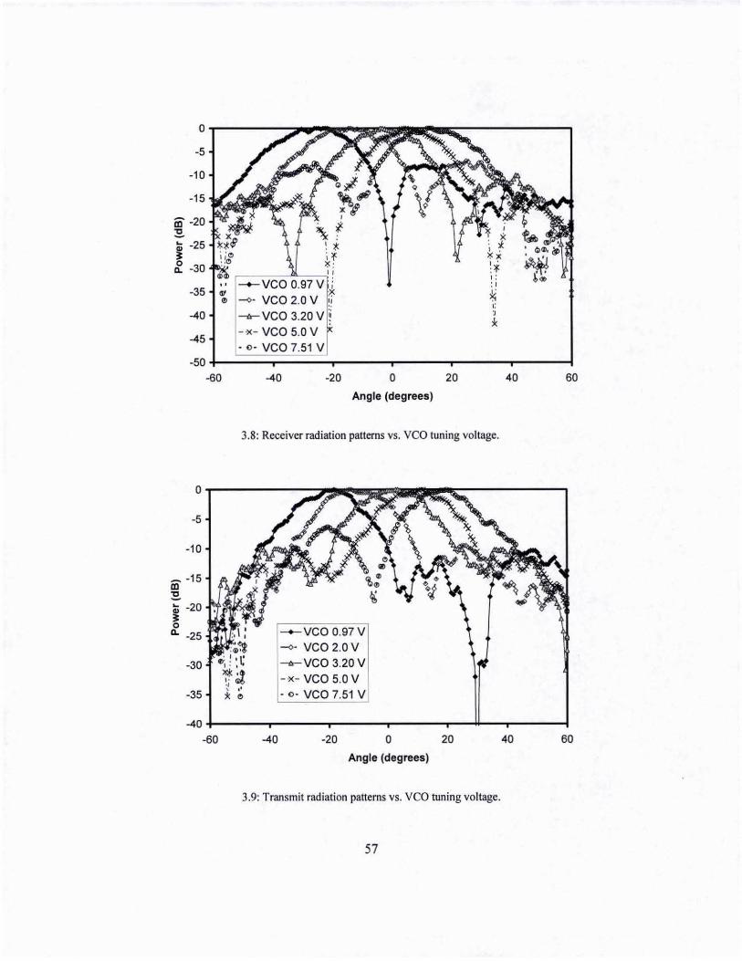
-5
-10
-15
iii" -20 :!!. G:i -25 ~ !t -30
-35 OJ ., -40
-45
, . ~x , . ., i: " ,. ~ " , *
. o · veo 7.51
·50 .J--=~==:"'---'------'---""T"'""----1 -60 -40 -20 o 20 40 60
Angle (degrees)
3.8: Receiver radiation patterns vs. veo tuning voltage.
0
-5
-10
_ -1 5 CD :!!. ~ -20 .. ~ 0
Q. ·25 -0. veo 2.0V
-30 -<>- veo 3.20 V _·x- veo 5.0 V
-35 . o· veo 7.51 V
-40 -60 -40 -20 o 20 40 60
Angle (degrees)
3.9: Transmit radiation patterns vs. veo tuning voltage.
57

3.4 Two-Dimensional Transmit, Voltage-ControHed Phased Array
For many applications two-dimensional steering arrays are required. This section
describes the first step into turning the topology of the one-dimensional full-duplex
frequency-controlled phased array into two-dimensional frequency-controlled phased
array by demonstrating two-dimensional transmission.
3.4.1 Two-Dimensional Beam Steering
Phase addition is used to achieve steering in the azimuth and elevation planes by
mixing LO and IF signals [31]. The example in Fig. 3.10 depicts IF and LO beam
forming networks with progressive phase delays across each row and column ports. The
mixer produces a signal containing the sum of the two phases. The columns contain the
IF beam-forming phase progressions, while the rows contain the LO beam-forming pbase
progressions. Column pbase progression steers the beam in the horizontal dimension,
and row phase progression steers the beam in the vertical dimension.
58
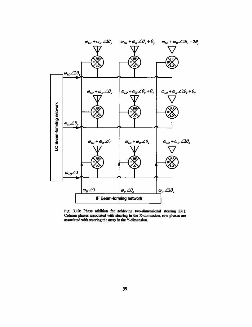
i!!
i c 01 .E E .e, j 0 -'
OJw +OJ/FL(}y OJw + OJ/FL(}. + (),. (iJw + (iJ/FL28. +~.
OJwL(),.
OJw +OJ1pLO (iJw + OJIPL(), OJw + OJ1FL28.
r-..L.(J}.:;IF:;..L_O ____ ...J._(J}..!�F:;..L:.:.:.;e.~ ___ ....L...,(J}IFL2(}.
IF Beam-forming network
Fig. 3.10: Phase addition for acldevlng two-dImensinna1 steering [31]. Column phases associated with steering in the X-dimension, row phases are associated with steering the array in the Y -dimension.
59
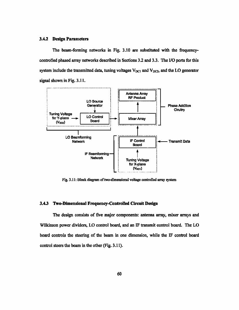
3.4.2 Design Parameters
The beam-forming networks in Fig. 3.1 0 are substituted with the frequency-
controlled phased array networks described in Sections 3.2 and 3.3. The 110 ports for this
system include the transmitted data, tuning voltages V DCI and V DC2, and the LO generator
signal shown in Fig. 3.11.
'-'~-.'---.. ~'-~---.---------------- .. ' .. --' .. ---". ! ! fl······ .. ~·~- ""'11 i ! ! RF Product 1 . LOSource ! i i : i ~GeneraIor ! j • 1 1
! Tuning Voltage ! ir---.....:----,i i for Y -plane _ LO Control +-- II Mixer Array Ii
(VDC2) Board i i.I",. =====~.i
I
Phase Addition CIruJtry
l ................................................................ : ........... · .. · .... t .. _ ........ -.... . LO e:~lng f .... · .. ·;~~;;;;; ........ ll-Transmit Data
IF Beamformlng Network
i l
Tuning Voltage ! i for X-plane :
(VQC1) i ... , ....... "'" __ .. ___ .. _ J
t
Fig. 3.11: Block diagram oftwo-dlmenslonal voltage controUed array system
3.4.3 Two-Dimensional Freqnency-ControUed Clrenit Design
The design consists of five major components: antenna array, mixer arrays and
Wilkinson power dividers, LO control board, and an IF transmit control board. The LO
board controls the steering of the beam in one dimension, while the IF control board
control steers the beam in the other (Fig. 3.11).
60
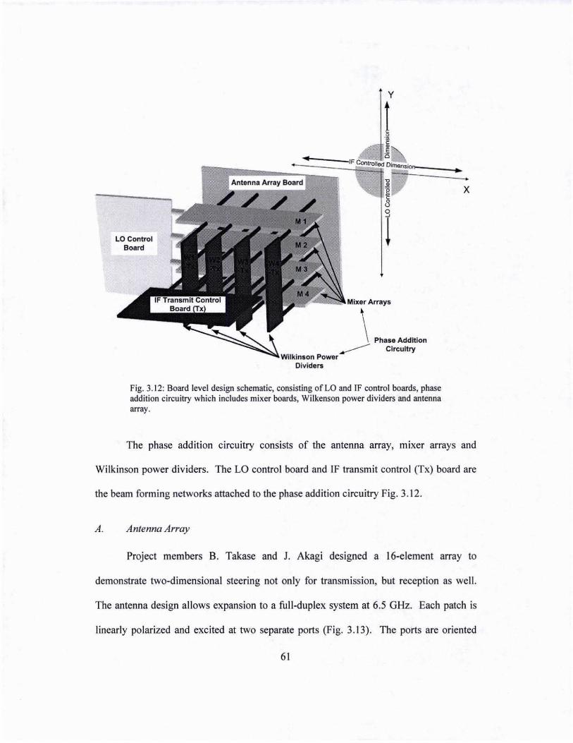
LO Control Board
Wilkinson Power Divider'
1
\ Pha.e Addition _______ Circuitry
Fig. 3. 12: Board level design schematic, consisting ofLO and IF control boards, phase addition circuitry which includes mixer boards, Wilkenson power dividers and antenna array.
x
The phase addition c ircuitry consists of the antenna array, mixer arrays and
Wilkinson power dividers. The LO control board and I F transmit control (Tx) board are
the beam forming networks attached to the phase addition circuitry Fig. 3.12.
A. Antenna Array
Project members B. Takase and 1. Akagi designed a 16-element array to
demonstrate two-dimensional steering not only for transmission, but reception as well.
The antenna design allows expansion to a full-duplex system at 6.5 GHz. Each patch is
linearly polarized and excited at two separate ports (Fig. 3.13). The ports are oriented
61
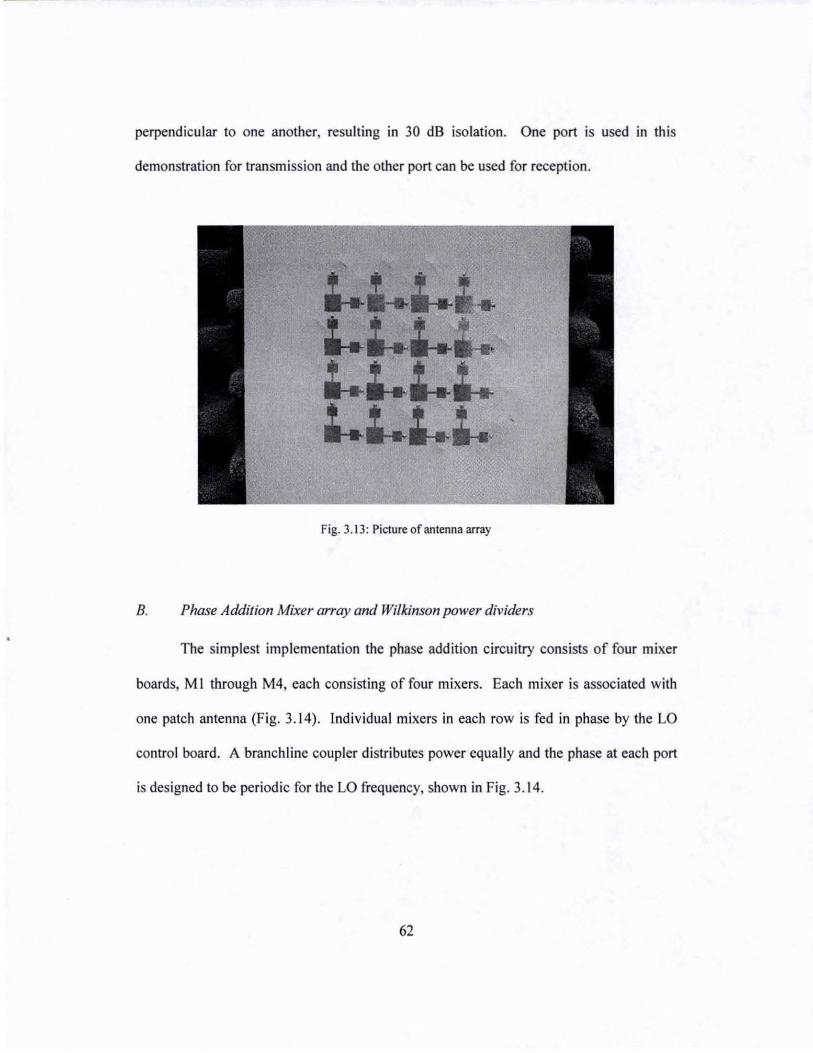
perpendicular to one another, resulting in 30 dB isolation. One port is used in this
demonstration for transmission and the other port can be used for reception.
,
Fig. 3.13: Picture ofantenn. arr.y
B. Phase Addition Mixer array and Wilkinson power dividers
The simplest implementation the phase addition circuitry consists of four mixer
boards, M I through M4, each consisting of four mixers. Each mixer is associated with
one patch antenna (Fig. 3.14). Individual mixers in each row is fed in phase by the LO
control board. A branchline coupler distributes power equally and the phase at each port
is designed to be periodic for the LO frequency, shown in Fig. 3.14.
62
!LJJ c 4.0 GHz
--+
TransmK Frequency f.. c 6.5 GHz
9+21r 9+61T
Fig. 3.14: Schematic of mixer board array,ldentlcs1 for boards MI tbrough M4 in Fig. 3.12 and Fig. 3.IS.
Fig. 3.14 depicts the schematic for an individual board. To complete the phase
addition circuitry, individual mixers in any given column are fed in phase by the same IF
signal. As shown in Fig. 3.12, the mixer boards MI through M4 are stacked horizontally
forming rows. Vertically oriented Wilkinson power dividers (Fig. 3.12 and Fig. 3.15,
WI-Tx through W4-Tx) feed the transmit mixers a 2.5-GHz signal at the IF ports in
columns.
The mixers combine the LO signal fLO = 4.0 GHz with the IF signal fIF = 2.5
GHz. The mixed product is transmitted at fRF = 6.5 GHz. Fig. 3.15 substitutes the phase
addition circuitry in the block diagram (Fig. 3.12) and depicts the 16 mixers required for
transmission.
63
Tuning Voltage for _
V-plane (VDC2)
LO Source W1-Tx Generator
IF Control Board
Tuning Voltage for X-plane (voc,)
_ Transmit Data
Fig. 3.15: Phase addition schematic substituted Into block diagram ofF!g. 3.11
c. IF transmit control board
• • •
The transmit control board controls the steering of the beam in the horizontal
dimension. The branchline coupler, mixers, and veOs used in the one-dimensional
array are used in the transmit IF control board. As the veo frequency changes, the
phase progression at each element changes accordingly, achieving beam steering.
For demonstration purposes the transmit frequency is selected at /IF = 2.5 GHz.
The signal is mixed with the veo signal /veo = (5.8-6.8) GHz and produces /RF = (8.3-
9.3) GHz. The /RF signal is mixed with the /veo producing a/IF = 2.5 GHz(Fig. 3.16).
64
Output Frequency flF " 2.5 GHz
W1-Tx W2-Tx W3-Tx W4-Tx
r ______________ J ________ t _______ t _______ J __ .
veo, fvco = (5.8-6.8) GHz
9+4cp
t Trensm~ Frequency
flF = 2.5 GHz
IF Transmit Control Board
Fig. 3.16: Schematic oflF tnmsmlt control board.
D. LO control board
The LO control board uses the same topology as the IF transmit control board.
The differences are signal frequencies and the amplifiers at the output stage. To avoid
variances in the output power of the radiated signal, the mixers in the mixer array boards
(MI through M4) must operate in the saturated region. The LO control board is fed
with a 4.0-GHz external signal source. The external source determines the output
frequency of the LO board array.
Like the other control boards, the branchline coupler provides the phase delay to
obtain the correct phase progression. From Fig. 3.1 7, the same model yeO used in the
65
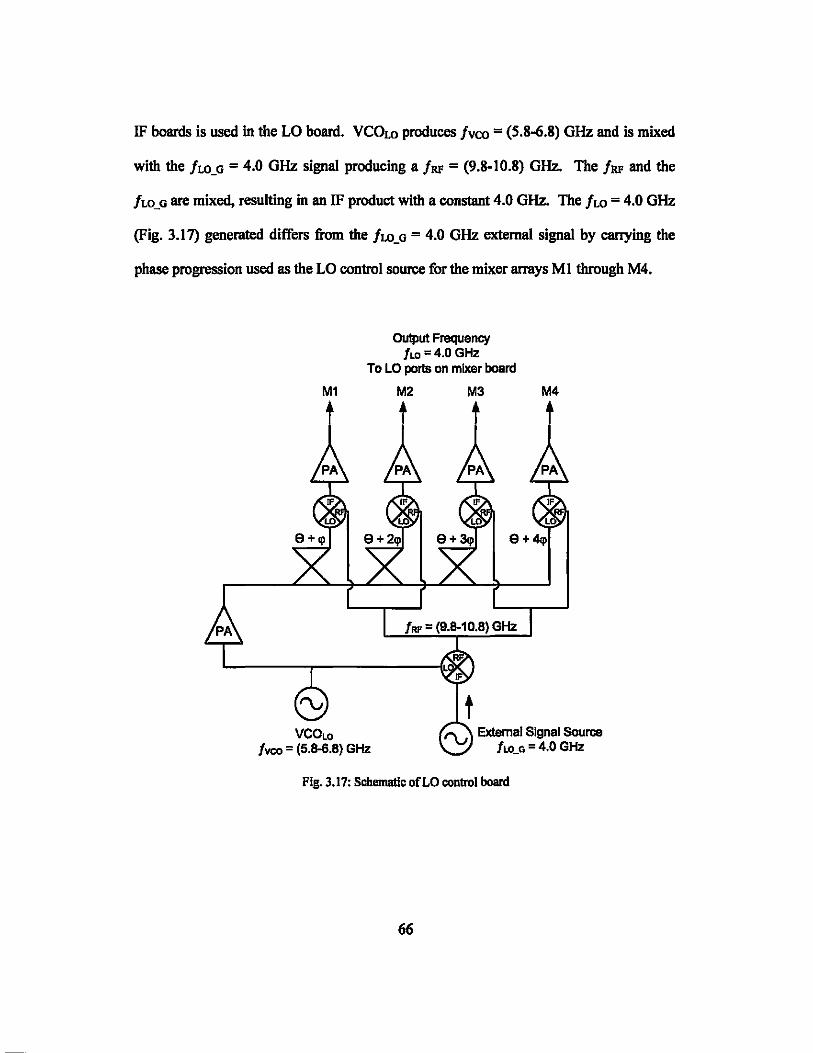
IF boards is used in the LO board. VCOLO produces Ivco = (5.8-6.8) GHz and is mixed
with the lLO_o = 4.0 GHz signal producing a IRF = (9.8-10.8) GHz. The IRF and the
lLO 0 are mixed, resulting in an IF product with a constant 4.0 GHz. The /Lo = 4.0 GHz
(Fig. 3.17) generated differs from the lLO_o = 4.0 GHz externaI signal by carrying the
phase progression used as the LO control source for the mixer arrays MI through M4.
Output Frequency fLO =4.0 GHz
To LO ports on mixer board
M1 M2 M3 M4
VCOlO fvco = (5.8-6.8) GHz
t
e+4<p
'\..i Extemal Signal Source flo_G = 4.0 GHz
Fig. 3.17: Schematic of LO control board
66
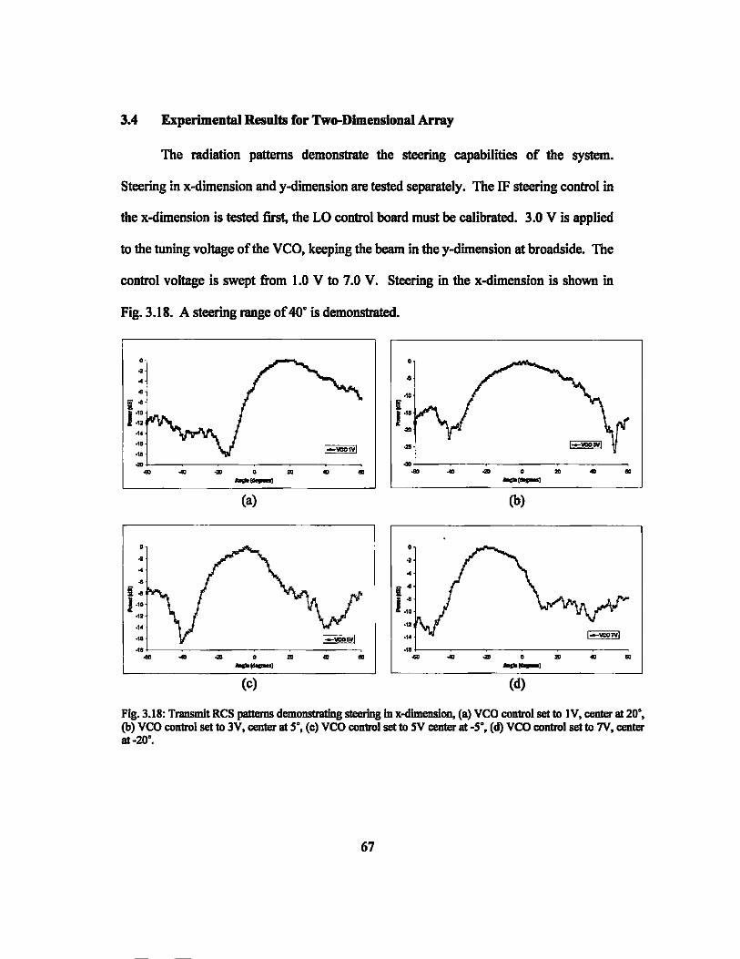
3.4 Experimental Results for Two-Dlmeusional Array
The radiation patterns demonstrate the steering capabilities of the system.
Steering in x-dimension and y-dimension are tested separately. The IF steering control in
the x-dimension is tested first, the LO control board must be calibrated. 3.0 V is applied
to the tuning voltage of the veo, keeping the beam in the y-dimension at broadside. The
control voltage is swept from 1.0 V to 7.0 V. Steering in the x-dimension is shown in
Fig. 3.18. A steering range of 40· is demonstrated.
• • • • • • .111
;:- I r: )"" . " .. •• ." 1_\'COwl .. .. ... '"
.., ... • " ., .. ... .., ... • " .. --, --
(a) (b)
• • •
;:' I.~ ." ." ...
.co ... • " .. ., .., .., .. • " .. --, --(c) (d)
.,
.,
Fig. 3.18: Transmit RCS patterns demonsbating steering in x-dimension, (a) veo control set to IV, center at 20·, (b) veo control set to 3V, center at 5·, (c) veo control set to SV center at -5·, (d) veo control set to 7V, center at ·20·.
67
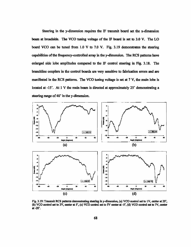
Steering in the y-dimension requires the IF transmit board set the x-dimension
beam at broadside. The veo tuning voltage of the IF board is set to 3.0 V. The LO
board veo can be tuned from 1.0 V to 7.0 V. Fig. 3.19 demonstrates the steering
capabilities of the frequency-controlled array in the y-dimension. The ReS patterns have
enlarged side lobe amplitudes compared to the IF control steering in Fig. 3.18. The
branchline couplers in the control boards are very sensitive to fabrication errors and are
manifested in the ReS patterns. The veo tuning voltage is set at 7 V, the main lobe is
located at -IS'. At I V the main beam is directed at approximately 25' demonstrating a
steering range of 40' in the y-dimension .
• .. • ~
~~ J.to
." ... ...
." .,,~----------------------... ... -aD 0 20 .. " JIqIa( ..... ,
(a)
~~-------------------------... ... . " AagIIt ldapns)
(c)
.. eo
~ 4 ~ a 20 • ~
.. ~ .. I-to ." ." .,.
...... '..-1 (b)
... ~-----------------------... ... . " /IIgIIICdeF-'
(d)
.. eo
Fig. 3.19: Transmit ReS ~ demonstrating steering Iny-dlmenslon, (a) veo control set to IV, center at 20', (b) veo control set to 3V, center at 5', (e) veo control set to sv center at -5', (d) veo control set to 7V, center at -20'.
68

A full-duplex frequency controlled array has been demonstrated in Section 3.2.
The frequency-controlled method has also been demonstrated in a two-dimensional
transmit array. The two-dimensional transmit array is expandable to a full-duplex array
and discussed in Section S.2A. The simple steering control of the frequency-controlled
array allows for easy system integration with control hardware. Possible integration of
self-steering control which is based on phase detection and power detection are discussed
in Section S.2B and S.2C respectively.
69
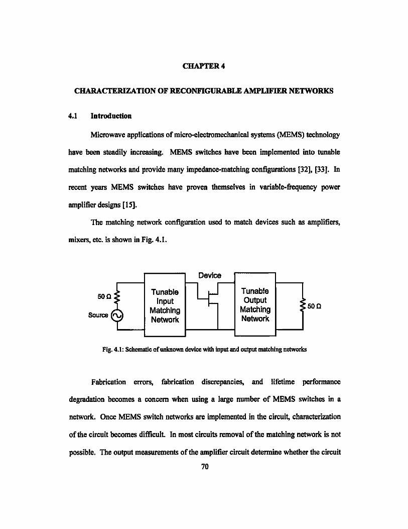
CHAPTER 4
CHARACTERIZATION OF RECONFIGURABLE AMPLIFIER NETWORKS
4.1 Introduction
Microwave applications of micro-electromechanical systems (MEMS) technology
have been steadily increasing. MEMS switches have been implemented into tunable
matching networks and provide many impedance-matching configurations [32]. [33]. In
recent years MEMS switches have proven themselves in variable-frequency power
amplifier designs [IS].
The matching network configuration used to match devices such as amplifiers,
mixers. etc. is shown in Fig. 4.1.
Tunable Input
Matching Network
Device
Tunable Output
Matching Network
Fig. 4.1: Schematic of unknown device with input and output matching networks
500
Fabrication errors, fabrication discrepancies. and lifetime performance
degradation becomes a concern when using a large number of MEMS switches in a
network. Once MEMS switch networks are implemented in the circuit, characterization
of the circuit becomes difficult In most circuits removal of the matching network is not
possible. The output measurements of the amplifier circuit detennine whether the circuit
70
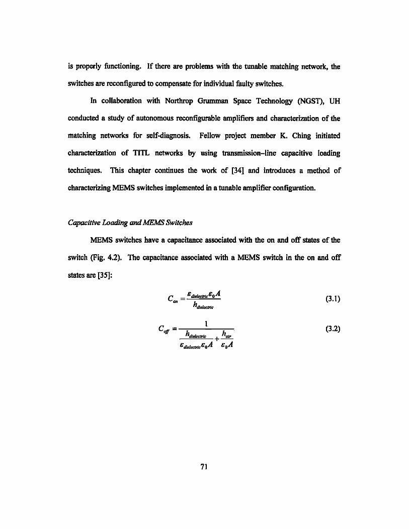
is properly functioning. If there are problems with the tunable matching network, the
switches are reconfigured to compensate for individual faulty switches.
In collaboration with Northrop Grumman Space Technology (NGST), UH
conducted a study of autonomous reconfigurable amplifiers and characterization of the
matching networks for self-diagnosis. Fellow project member K. Ching initiated
characterization of TIlL networks by using transmission-line capacitive loading
techniques. This chapter continues the work of [34] and introduces a method of
characterizing MEMS switches implemented in a tunable amplifier configuration.
Capacitive Loading and MEMS Switches
MEMS switches have a capacitance associated with the on and off states of the
switch (Fig. 4.2). The capacitance associated with a MEMS switch in the on and off
states are [35]:
Con (3.1)
(3.2)
71
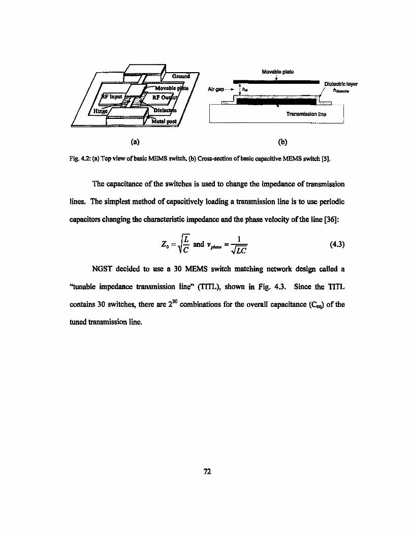
Movable plata ................... , DIe_layer A1rgap---~ 1"" i h_
~>"'H\ rb [ T_nne u1
(a) (b)
Fig, 4.2: (a) Top view of basic MEMS switch. (b) Cross-section of basic capacitive MEMS switch [5).
The capacitance of the switches is used to change the impedance of transmission
lines. The simplest method of capacitively loading a transmission line is to use periodic
capacitors changing the characteristic impedance and the phase velocity of the line [36]:
(4.3)
NGST decided to use a 30 MEMS switch matching network design called a
''tunable impedance transmission line" (TlTL). shown in Fig. 4.3. Since the TITL
contains 30 switches, there are 230 combinations for the overall capacitance (Ceq) of the
tuned transmission line.
72
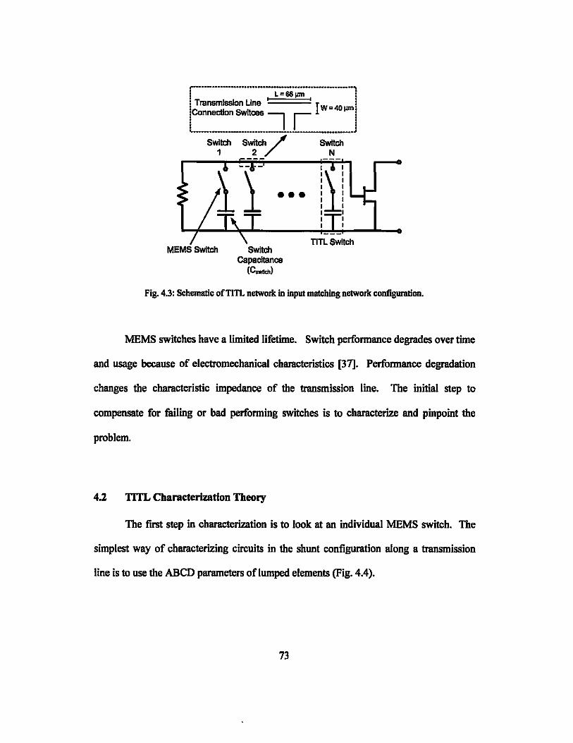
r··········--········~;;,;;···-·······--l I I • i Transmlsslon Una I W. 40 pm i IConnecUon SWItces I I J '---.. _ .... _--_._ ... _ .. _ .. __ .... -
Switch Switch "" SwItch 1 2 ~ N
MEMSSwItch
•••
SwItch Capacitance
(C-)
III I I I I I I I I I I I I I I I I
TlTL SwItch
Fig. 4.3: Schematic ofTITL networl< in input matching network configuration.
MEMS switches have a limited lifetime. Switch perfonnance degrades over time
and usage because of electromechanical characteristics [37]. Perfonnance degradation
changes the characteristic impedance of the transmission line. The initial step to
compensate for failing or bad perfonning switches is to characterize and pinpoint the
problem.
4.2 TITL Characterization Theory
The first step in characterization is to look at an individual MEMS switch. The
simplest way of characterizing circuits in the shunt configuration along a transmission
line is to use the ABeD parameters oflumped elements (Fig. 4.4).
73
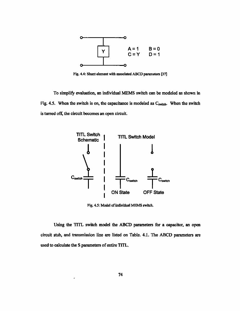
J y A=1 B=O
e=y D=1
I Fig. 4.4: Shunt element with associated ABCD parameters [37]
To simplify evaluation, an individual MEMS switch can be modeled as shown in
Fig. 4.5. When the switch is on, the capacitance is modeled as Cswm:t.. When the switch
is turned ort: the circuit becomes an open circuit.
TITLSwitch I TITL Switch Model Schematic
! I ! I
0-1 I I ..l
T I Te- Te-I I ON State OFF State
Fig. 4.5: Model ofindMdual MEMS switch.
Using the TITL switch model the ABCD parameters for a capacitor, an open
circuit stub, and transmission line are listed on Table. 4.1. The ABCD parameters are
used to calculate the S parameters of entire TITL.
74
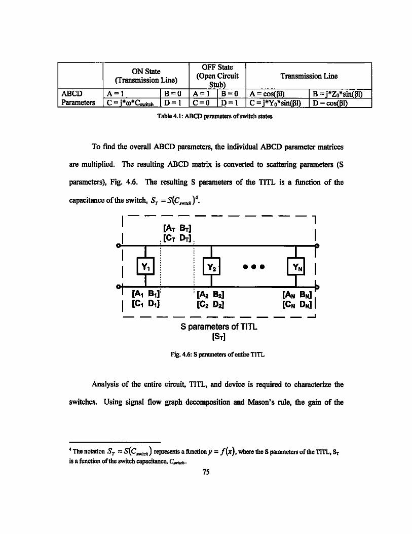
ON State OFF State
(Open Circuit Transmission Line (Transmission Line) Stub)
ABCD A= I TB=O A=I I B=O A - coslBJ) B = j*Zo*sin(!3l) Parameters C = j*m*CIIWitcb I D = I C=O I D=I C = j*Y o·sin(l3l) D = cosl!3l)
Table 4.1: ABCD parameters of switch states
To find the overall ABCD parameters, the individual ABCD parameter matrices
are multiplied. The resulting ABCD matrix is converted to scattering parameters (S
parameters), Fig. 4.6. The resulting S parameters of the TITL is a function of the
capacitance of the switch, S7 = S(C_rdY.
II
------1 [AT B-r] [CT D-r].
• ••
S parameters of TITL 1ST]
Fig. 4.6: S parameters of entire TITL
I
---I
Analysis of the entire circuit, TITL, and device is required to characterize the
switches. Using signal flow graph decomposition and Mason's rule, the gain of the
4 The notation S7 = S(C .... Uch ) represents a functiony = f(x), where the S parameters oflhe TITL, Sr is a function oflhe switch c:apacitance. C,.."",.
75
amplifier circuit can be detennined from the S parameters of the TITL and device (Fig.
4.7).
-I I I -
TITL I Device [5T]
I [So]
II I -
Measured gain
I I I ---------------- --- - --------~--------
Fig. 4.7: Schematic of cin:uit S panuneters, Sr - S panuneters of the TITL, So - S panuneters of the device
Using Mason's rule, the gain of the circuit is
(4.4)
There are four unknowns, S2lD and SllD of the device and the S2ly and Sllr of the
TITL. S2lT and SI ly are symbolically expanded in tenns ofc..- and substituted back
into (4.4) resulting in
(4.5)
Substituting the TITL S parameters in terms of Cswitclb the gain equation now consists of
three unknowns, Cawm:J" S2lD and SlID.
4.3 SymhoRc Analysis
To solve for each variable, each of the three gain equations must contain all the
variables. The simplest method of obtaining the three different equations is reconfiguring
two switches in the TITL. Simplifying the 30 switch TITL, the first two switches are
76
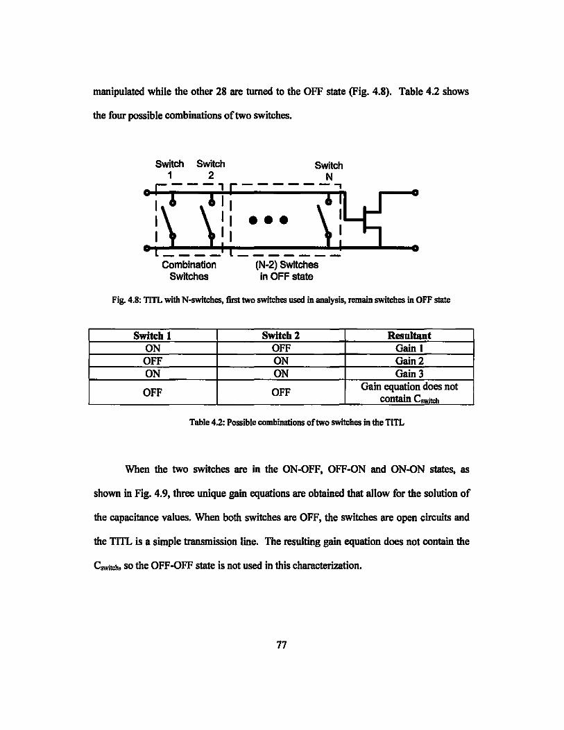
manipulated while the other 28 are turned to the OFF state (Fig. 4.8). Table 4.2 shows
the four possible combinations of two switches.
Combination Switches
Switch N ------,
••• (N-2) Switches In OFF state
Fig. 4.8: TlTL with N-switches, first two switches used in analysis, remain switches in OFF state
Switch 1 Switch :z Resultant ON OFF Gain I OFF ON Gain 2 ON ON Gain 3
OFF OFF Gain equation does not contain Cswitoh
Table 4.2: Possible combinations of two switches in the TlTL
When the two switches are in the ON-DFF, OFF-ON and ON-ON states, as
shown in Fig. 4.9, three unique gain equations are obtained that allow for the solution of
the capacitance values. When both switches are OFF, the switches are open circuits and
the TITL is a simple transmission line. The resulting gain equation does not contain the
Cswru:b, so the OFF-OFF state is not used in this characterization.
77
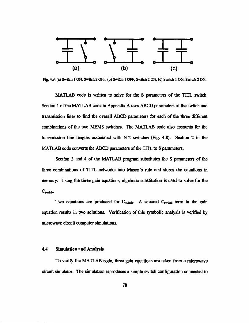
I I ~
I I I I II I I
I I • .I I • (a) (b) (c)
Fig. 4.9: (a) Switch ION, Switch 2 OFF, (b) Switch I OFF, Switch 2 ON, (c) Switch ION, Switch 2 ON.
MATLAB code is written to solve for the S parameters of the TITL switch.
Section I of the MA TLAB code in Appendix A uses ABeD parameters of the switch and
transmission lines to find the overall ABeD parameters for each of the three different
combinations of the two MEMS switches. The MATLAB code also accounts for the
transmission line lengths associated with N-2 switches (Fig. 4.8). Section 2 in the
MA TLAB code converts the ABeD parameters of the TITL to S parameters.
Section 3 and 4 of the MA TLAB program substitutes the S parameters of the
three combinations of TITL networks into Mason's rule and stores the equations in
memory. Using the three gain equations, algebraic substitution is used to solve for the
Cswitd..
Two equations are produced for Cswitd.. A squared Cswitd. term in the gain
equation results in two solutions. Verification of this symbolic analysis is verified by
microwave circuit computer simulations.
4.4 Slmulatiou aud Analysis
To veritY the MATLAB code, three gain equations are taken from a microwave
circuit simulator. The simulation reproduces a simple switch configuration connected to
78
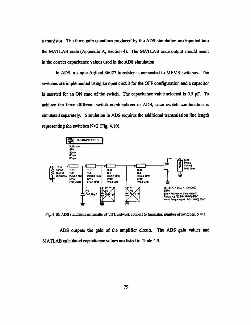
a transistor. The three gain equations produced by the ADS simulation are inputted into
the MATLAB code (Appendix A. Section 4). The MATLAB code output should result
in the correct capacitance values used in the ADS simulation.
In ADS, a single Agilent 36077 transistor is connected to MEMS switches. The
switches are implemented using an open circuit for the OFF configuration and a capacitor
is inserted for an ON state of the switch. The capacitance value selected is o.s pF. To
achieve the three different switch combinations in ADS, each switch combination is
simulated separately. Simulation in ADS requires the additional transmission line length
representing the switches N>2 (Fig. 4.10).
=
I ~ I S.PARAMETERS I
"'"
S_Pamtn SP1 StaJIo ...... ......
Tenn1 TUN Numo1 lL2 Zc&O Ctun Zc6D.D
E010 F=2.4BHz
11.IN TL3 z.«I,O Olun E010 F<>2.4 GHz
c C2
11.'N 11.1 Za5D.Oaun EQ10 1'=2.4 GHz
1 """.10pF
• '.I;t .. / ~.1
," "', '.
=
11.1N 11.4 _0 Ohm £010 _4GHz
,.--f'LT ....
=
T..." N""," Zo5OO1Im
Fig. 4.10: ADS slmu\atlon schematic ofTiTL network connect to transistor, nwnber of switches, N = 3.
ADS outputs the gain of the amplifier circuit. The ADS gain values and
MATLAB calculated capacitance values are listed in Table 4.3.
79
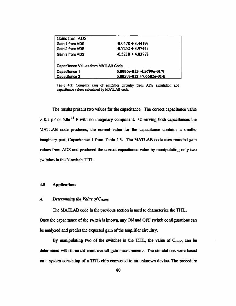
Gains from ADS Gain 1 from ADS Gain 2 from ADS
Gain 3 from ADS
-0.0478 + 3.4419i -0.7252 + 3.9744i -0.5218 + 4.0377i
Capacitance Values from MATlAB Code
Capacitance 1 5.0006tHJ13 -4.5799e-0171 Capacitance 2 5.8850e-012 +7.6682e-014i
Table 4.3: Complex gain of amplifier circuitry from ADS simulation and capacitance values calculated by MA TLAB code.
The results present two values for the capacitance. The correct capacitance value
is 0.5 pF or 5.0e·13 F with no imagiruuy component Observing both capacitances the
MA TI.AB code produces, the correct value for the capacitance contains a smaller
imaginary part, Capacitance 1 from Table 4.3. The MATLAB code uses rounded gain
values from ADS and produced the correct capacitance value by manipulating only two
switches in the N-switch TlTL.
4.5 AppUcations
A. Determining the Value ofCsw/1ch
The MA TLAB code in the previous section is used to characterize the TlTL.
Once the capacitance of the switch is known, any ON and OFF switch configurations can
be analyzed and predict the expected gain of the amplifier circuitry.
By manipulating two of the switches in the TITL, the value of c.- can be
determined with three different overall gain measurements. The simulations were based
on a system consisting of a TITI. chip connected to an unknown device. The procedure
80
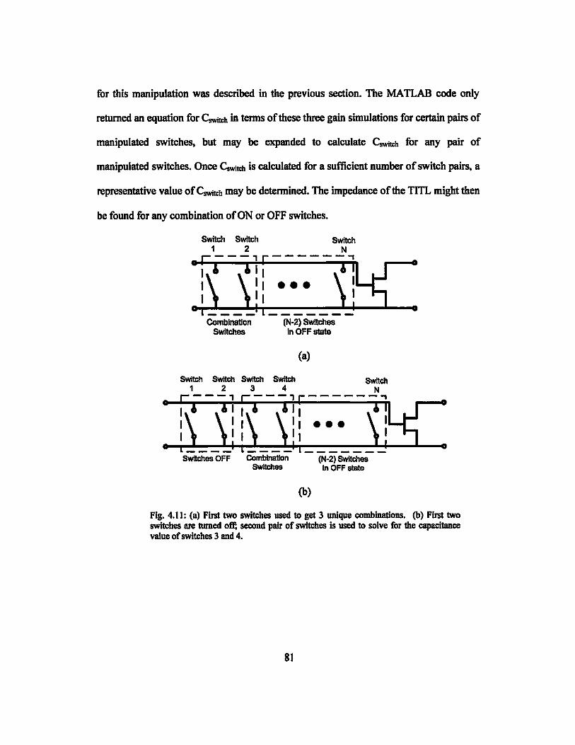
for this manipulation was described in the previous section. The MA TLAB code only
returned an equation for CswitclI in terms of these three gain simulations for certain pairs of
manipulated switches, but may be expanded to calculate CswitclI for any pair of
manipulated switches. Once CswitclI is calculated for a sufficient number of switch pairs, a
representative value of CswitclI may be determined. The impedance of the TITL might then
be found for any combination of ON or OFF switches.
Combination Switches
Switch N ------.,
••• (N·2) Switches In OFF state
(a)
SwiIch Swftch N -------,
••• Switches OFF Combination (N·2) Swftches
Swftches In OFF .-
(b)
Fig. 4.11: (a) First two switches used to get 3 unique combinations. (b) First two switches are turned off, second pair of switches is used to solve for the capacitance value of switches 3 and 4.
81

B. Testingfor Faulty Switches in the TITL
Once the value of C- is found as described above. faulty switches can be tested
for while the TITL is embedded with the unknown device. A single switch can be set to
the ON state while the rest of the switches are left in the OFF state.
Since the value ofC-. S21D. and SliD were previously solved, the gain of the
entire circuit can be calculated for any configuration of the TITL. A faulty TITL switch
can be detected by comparing the predicted gain value to the measured gain of the circuit
82
5.1 Conclusions
CHAPTER 5
CONCLUSIONS AND FUTURE WORK
This thesis presented advances in satellite-to-satellite communication systems,
mobile terrestrial to satellite systems, and a method of characterizing a class of
reconfigurable circuits.
A pair of nanosatellites was presented and discussed in Chapter 2, demonstrating
a 10.5-GHz two-dimensional retrodirective array for small-satellite communications.
The quadruple subharmonic mixing technique achieved phase conjugation and eliminated
the need for a high-frequency LO source. One satellite housed the eight-element two
dimensional array with eight circularly polarized patch antennas and communicated with
a transponder satellite.
A one-dimensional and two-dimensional voltage-controlled analog phased array
was described and verified in Chapter 3. Many mobile communication systems require
a fast tracking highly directive communication link. Electronically steered arrays provide
fast analog operation. A scanning range of 40· was demonstrated in one-dimension and a
scanning range of 40' in each axis in shown in the two-dimensional prototype.
As the demand for multi-frequency communications increases so does the demand
for MEMS tunable matching networks. Chapter 4 introduced a simplification of
unknown MEMS switches in a TIlL and a method for switch characterization.
MA TLAB solving code was written requiring only three gain measurements of the
83

amplifier module. The characterization code was verified using ADS simulation gain
measurements.
5.2 Suggestions for Future Work
A. Two-dimensional Full-duplex Frequency-Controlled Phased A"DY
The full-duplex capabilities demonstrated in one-dimensional frequency
controlled array in Section 3.2 can be applied to the two-dimensional transmit frequency
controlled array demonstrated in Section 3.4. A receiving two-dimensional frequency
controlled array is easily integrated into the current two-dimensional transmit system by
creating another set of mixer arrays and a set of mirror image LO and IF control boards
(Fig. 5.1 and Fig. 5.2). Like the one-dimensional array, two sets of circuitry are
implemented, one for transmission and the other for reception. The antenna array in
Section 3.4.3A has been designed with full-duplex expansion capabilities. One
polarization plane of the antenna will be dedicated for transmission and the other for
reception. The control voltages for both systems are linked together, receive and transmit
arrays steer simultaneously in the same direction (Fig. 5.3).
84
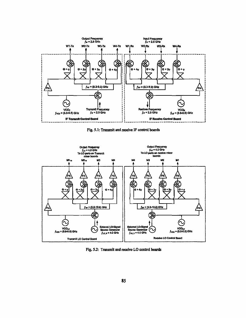
OuIpulF_ IIIPUIF_ /" III 2.6 GHz /$ a 2.8 GHz
W1·T. W2·T. W3-T. W4-T. W1·Ax W2-Rx W3-Rx W4-Ax
r-------------J-------- ------- ------- --. r-J ______ J _______ J _______ t _____________ . : l! : I II' : I I I I I I I I I I I I I I
: 8+4J :: e.~ : : :: : I I I I
I 11 : : : I : : :: : : :: : I : I I
I: :
t TranomIIF_
1T1 A 2.6GHz
:: I : ::, : I I Rec:Iaw Frequency I
! ! fll'a2.6GHz ILOm{:'~8)GHz ! :: : ____________ ~_~~~~:~~~ _____________ : l _____________ ~~~~ _____________ l
M'm
veou, /vt:1l a (6.8-8.8) GHz
FIg. 5.1: Transmit and receive IF control boards
0UlIIUI_ fLO-4.00Hz
OUlIIUIFnIquency fl.O a 4.oGHz
To LO ports on TransmIl To LO ports on receIw mb:er --
t
M4
e ....
_ L<><!IgrIaI --11.1'-'1 a 4.0 GHz
-M4 M2
Fig. S.2: Tnmsmit and receive LO control boards
85
M'
veou, 1'Il00 a (5.8-8.8) GHz.
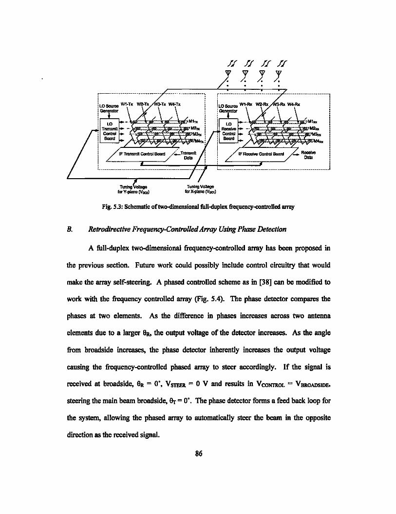
// // // //
J J J ---------------- ------1
I /Y1. I
._-- -.: I :.. ________________________________________________ ..1
r---------···------------------- ------- -----------, · . · . ! LO Source Wi-Tx W2·Tx !
i~ i I : · . ; t.O -- Min ! : Transmit -. M2nI ! : Control .. :
!-.. !
I ______ -----~-~=:-:---------- ____ .
Fig. 5.3: Schematic of two-dimensional tiIIl~uplex frequency-<ontrolled array
B. Retrodirective Frequency-Control1ed A"ay Using Phase Detection
A full-duplex two-dimensional frequency-controlled array has been proposed in
the previous section. Future work could possibly include control circuitry that would
make the array self-steering. A phased controlled scheme as in [38] can be modified to
work with the frequency controlled array (Fig. 5.4). The phase detector compares the
phases at two elements. As the difference in phases increases across two antenna
elements due to a larger IIR. the output voltage of the detector increases. As the angle
from broadside increases, the phase detector inherently increases the output voltage
causing the frequency-controlled phased array to steer accordingly. If the signal is
received at broadside, ea = 0', VSTEER = 0 V and results in VCONTROL = VBROADSJDE,
steering the main beam broadside, &r = 0'. The phase detector forms a feed back loop for
the system, allowing the phased array to automatically steer the beam in the opposite
direction as the received signal.
86
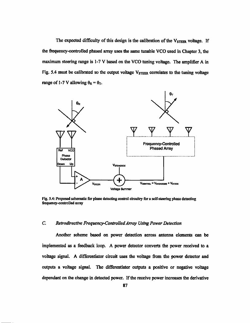
The expected difficulty of this design is the calibration of the V STEER voltage. If
the frequency-controlled phased array uses the same tunable veo used in Chapter 3, the
maximum steering range is 1-7 V based on the veo tuning voltage. The amplifier A in
Fig. 5.4 must be calibrated so the output voltage VSTEER correlates to the tuning voltage
range of 1-7 V allowing eR = &r.
ReI yeo
Phase De!ec!or
Down
, ... I._ ........ I .......... _I ........... I_ .. , , i Frequency-Conlrolled ! i Phased Array ! [ , i •. ___ •••••••. _ ................. _.. • •• _. ____ •••....•.•..•. _ .•• ..1
VCONlRCl. = VBROADSIDI! + VIiTEER
Fig. 5.4: Proposed schematic for phase detecting control circuitry for a seJf,.steering phase detecting fiequency-controlled an-ay
C. &trodirective Frequency-Controlled Array Using Power Detection
Another scheme based on power detection across antenna elements can be
implemented as a feedback loop. A power detector converts the power received to a
voltage signal. A differentiator circuit uses the voltage from the power detector and
outputs a voltage signal. The differentiator outputs a positive or negative voltage
dependant on the change in detected power. If the receive power increases the derivative
87
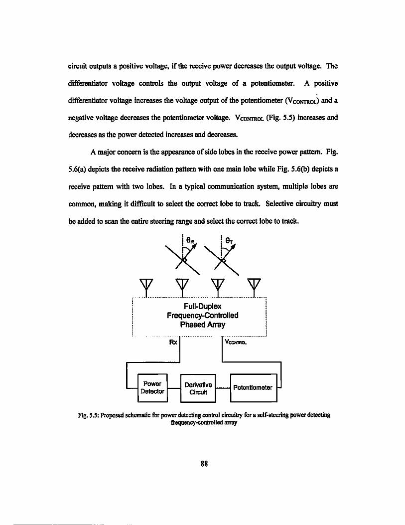
circuit outputs a positive voltage, if the receive power decreases the output voltage. The
differentiator voltage controls the output voltage of a potentiometer. A positive
differentiator voltage increases the voltage output of the potentiometer (V CONTROL) and a
negative voltage decreases the potentiometer voltage. V CONTROL (Fig. 5.5) increases and
decreases as the power detected increases and decreases.
A major concern is the appearance of side lobes in the receive power pattern. Fig.
5.6(a) depicts the receive radiation pattern with one main lobe while Fig. 5.6(b) depicts a
receive pattern with two lobes. In a typical communication system, multiple lobes are
common, making it difficult to select the correct lobe to track. Selective circuitry must
be added to scan the entire steering range and select the correct lobe to track.
~~ c.1 ..... _ ..... 1 ...... 1 .. _._ ... 1 ... , i i ! Full-Duplex i i Frequency-Controlled , i Phased Array i ! i -. .... -----~-.--- . ..... ~-.-.----- --- .. -----.---..... ~ ..
Rx v""""""
Power Derivative Potentiometer - Detector r- Clrcutt -
Fig. 5.5: Proposed schematic for power detecting ccn1rol circuitry for a self-steering power detecting frequency-controlled array
88
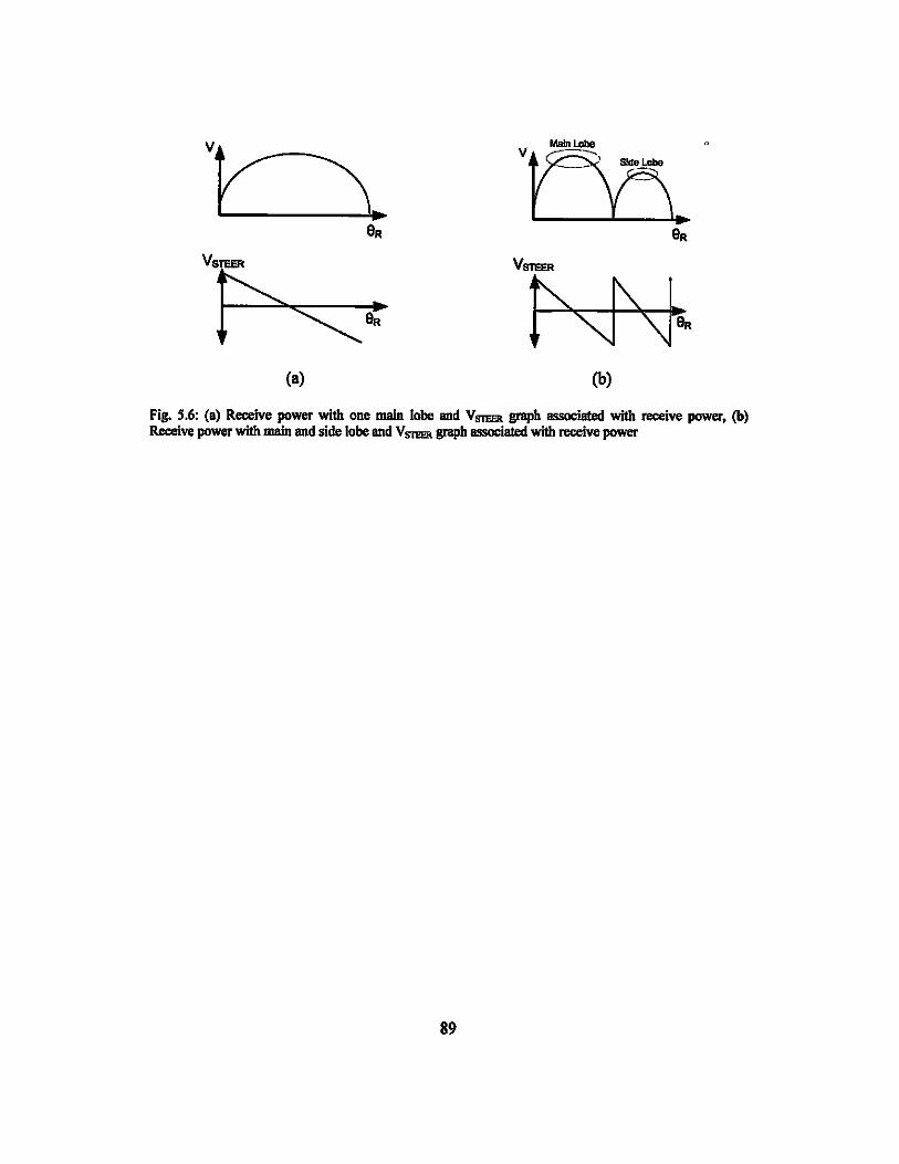
(a) (b)
Fig. 5.6: (a) Receive power with one main lobe and V!III!I!R graph associated with receive power, (h) Receive power with main and side lobe and V STI!ER graph associated with receive power
89
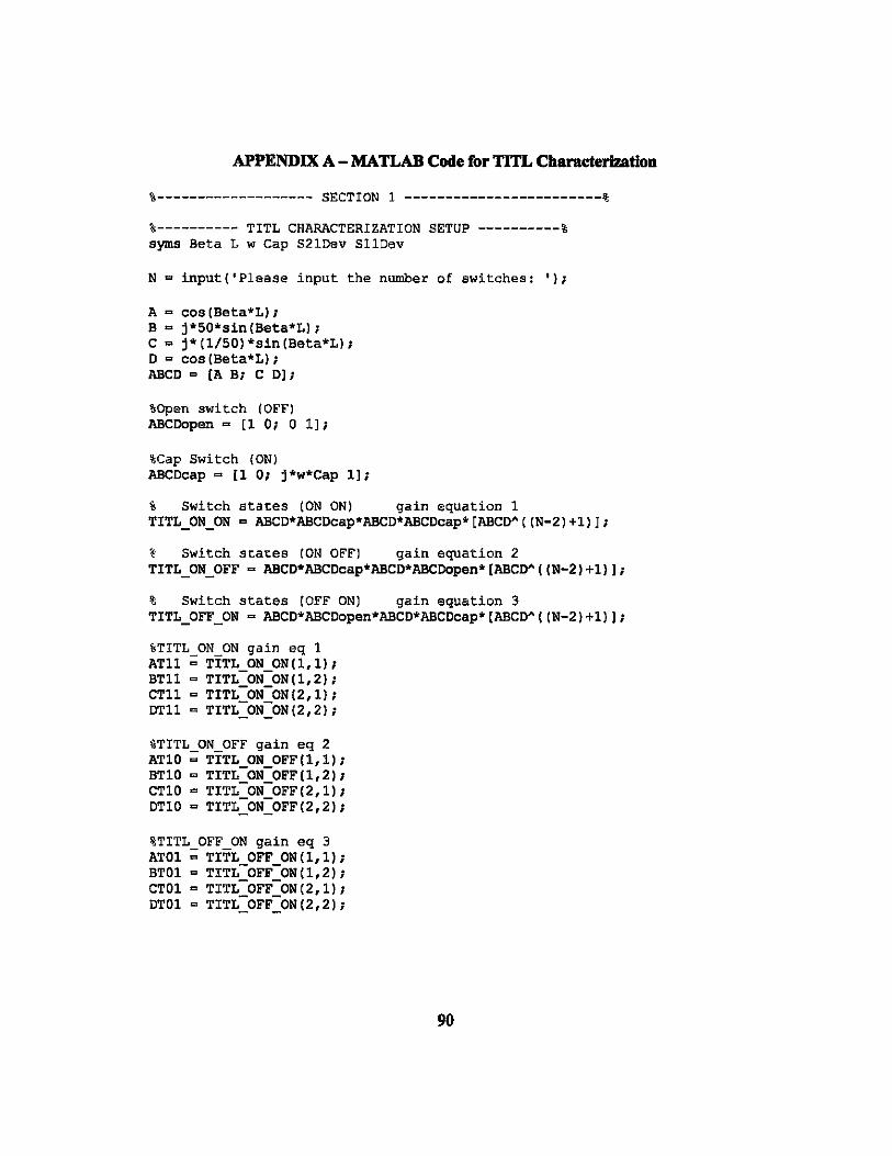
APPENDIX A - MATLAB Code for TlTL ChBJ'llderizatioD
%------------------- SECTION 1 ------------------------% %---------- TITL CHARACTERIZATION SETUP ----------% syrns Beta L w Cap S2lDev SllDev
N = input('Please input the number of switches: ');
A = cos(Beta*L); B = j*SO*sin(Beta*L); C = j*(l/SO)*sin(Beta*L); D = cos(Beta*L); ABCD = [A B; C D1;
%Open switch (OFF) ABCDopen = [1 0; 0 IJ;
%Cap Switch (ON) ABCDcap = [1 0; j*w*Cap 11;
% Switch states (ON ON) gain equation 1 TITL_ON_ON = ABCD*ABCDcap*ABCO*ABCOcap*[ABCOA «N-2)+1)J;
% Switch states (ON OrF) gain equation 2 TITL_ON_OFF = ABCO*ABCOcap*ABCO*ABCDopen*[ABCOA «N-2)+1)J;
% Switch states (OFF ON) gain equation 3 TITL_OFF_ON = ABCO*ABCOopen*ABCO*ABCOcap*[ABCOA {{N-2)+I)J;
%TITL_ON_ON gain eq 1 ATll = TITL ON ON{l,I); BTll = TITL-ON-ON{I,2); CTll = TITL-ON-ON(2,1); DTll = TITL:ON:ON(2,2);
%TITL ON OFF gain eq 2 ATIO ~ TITL ON OFF(I,I); BTIO = TITL-ON-OFF(I,2); CTIO = TITL-ON-OFF(2,l); OTIO = TITL:ON:OFF(2,2);
%TITL OFF ON gain eq 3 ATOl ~ TITL OFF ON(l,l); BTOl = TITL-OFF-ON(l,2); CTOl = TITL-OFF-ON{2,l); DTOl = TITL:OFF:ON{2,2);
90
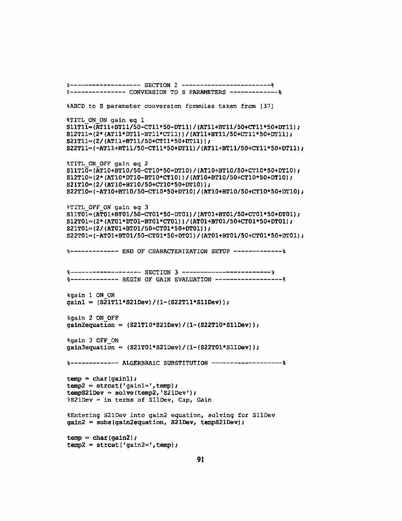
%------------------- SECTION 2 ------------------------~ %--------------- CONVERSION TO S PARAMETERS -------------% %ABCD to S parameter conversion formulas taken from [37]
%TITL ON ON gain eq I SIITIl=(ATII+BTII/SO-CTll*SO-DTI1)/(AT11+BTll/SO+CTll*SO+DTll); S12Tll=(2*(ATll*OTll-BTll*CTll))/(ATll+BTll/SO+CTll*SO+OTIl); S21Tll=(2/(ATll+BTll/S0+CTll*SO+OTll))/ S22Tll=(-ATll+BTI1/SO-CTI1*SO+OTll)/(ATII+BTll/S0+CTll*SO+OTll);
%TITL ON OFF gain eq 2 SIITIO=(ATIO+BTlO/SO-CTlO*SO-OTlO)/(ATIO+BTlO/SO+CTlO*SO+DTIO)/ S12TIO=(2*(ATIO*DTIO-BTIO*CTIO))/(ATIO+BTIO/SO+CTlO*SO+DTIO); S21TlO=(2/(ATlO+BTlO/SO+CTlO*SO+DTIO)); S22TlO=(-ATlO+BTlO/SO-CTlO*SO+DTlO)/(ATlO+BTlO/SO+CTlO*SO+DTlO);
%TITL OFF ON gain eq 3 SllTOl=(AT01+BT01/SO-CTOl*SO-OTOl)/(ATOl+BT01/SO+CTOl*SO+OTOl); S12T01=(2*(ATOl*OTOl-BTOl*CTOl))/(AT01+BT01/SO+CTOl*SO+DTO1); S2lT01=(2/(AT01+BT01/SO+CT01*SO+DT01))/ S22TOl=(-ATOl+BTOl/SO-CTOl*SO+DTOl)/(ATOl+BT01/SO+CTOl*SO+DTOl);
%------------- END OF CHARACTERIZATION SETUP -------------%
%------------------- SECTION 3 ------------------------~ %------------- BEGIN OF GAIN EVALUATION ------------------% %gain 1 ON ON gainl = (S2lTll*S2lDev)/(1-(S22Tll*SllDev));
%gain 2 ON OFF gain2equatIon = (S2lTlO*S2l0ev)/(1-(S22TlO*SllDev));
%gain 3 OFF ON gain3equation = (S21TOl*S2lDev)/(1-(S22TOl*SllDev));
~------------- ALGERBRAIC SUBSTITUTION -------------------% temp = char(gainl)/ temp2 = strcat('gainl=',temp); tempS21Dev = solve(ternp2,'S21Dev'); .S21Dev = in terms of SllDev, Cap, Gain
%Entering S21Dev into gain2 equation, solving for SllDev gain2 = subs(gain2equation, S21Dev, tempS21Dev);
temp = char(gain2); temp2 = strcat('gain2=',temp);
91

tempSllDev = solve(temp2, 'SIIDev');
%Using gain3, substituting S21Dev and SllDev, solving for cap tempgain3 = subs(gain3equation, S21Dev, tempS21Davl; gain3 = subs(tempgain3, SllDav, tempSllDev);
temp = char(gain3); temp2 = strcat('gain3~',templ;
,Solving for capacitance tempCap = solve(temp2, 'Cap');
%Displaying capacitance values (two values equation contains sqrt) capacitancel = (tempCap(I,I»; capacitance2 = (tempCap(2,l»;
%--------------- END OF SYMBOLIC ANALYSIS -------------%
%------------------- SECTION 4 ------------------------% ,--------------- START NUMERICAL ANALYSIS -------------% %INPUT FROM USER freq = input('\nPlease enter frequency (Hz) :'); wavelength = (3*10A 8)/(freq); eleclength = input('\nPlease enter electrical length of transmission lines (degrees): '); %END OF INPUT FROM USER
%2*pii(wavelength) Beta = (2*pi)/wavelength;
%Lengths of the transmission line (10 electrical degrees) L = (eleclength*pi/l80)/Beta;
%2*pi*(frequency)-----> 2.4 GHz w=2*pi*freq;
%Assuming Capacitance %Cap = .5*10'-12;
0.5 pF EXAMPLE VALUE
syrns gain1 gain2 gain3
%INPUT FROM USER gainl = input('\nEnter gainl switch config ON ON: '); %gainl = -0.0478 + 3.4419*i; % example taken from ADS
gain2 = input('\nEnter gain2 switch config ON_OFF: '); %gain2 = -0.7252 + 3.9744*i; %example from ADS
gain3 = input('\nEnter gain3 switch can fig OFF_ON: 'I; %gain3 = -0.5218 + 4.0377*i; %example from ADS %END OF INPUT FROM USER
92

%Oisplaying numerical value of capacitance capl = subs(capacitancel) cap2 = subs(capacitance2)
~--------------- END OF NUMERICAL ANALYSIS -------------%
93

REFERENCES
[I] "Sea Launch to Launch Two Spaceway Satellites." Retrieved July 03, 2006 from, www.spaceandtech.com.
[2] "Satellite seeks broadband re-entry." Retrieved July 03, 2006 from, news.com.com.
[3] "SPACEWA yTM North America." Retrieved July 03, 2006 from, www.boeing.com.
[4] HONOLULU ADVERTISER, 2005. Marine's ability to communicate on the run gets a boost. Honolulu Advertiser, 9 Sep. 2005.
[5] M. Skolnik, Introduction to Rodar Systems. Second Edition. New York: McGraw-HilI Book Company, 1980.
[6] E. Pels and W. Liang, "A method of array steeriog by means of phased control through heterodyoing," IRE 7rans. Antennas Propagot., vol. AP-IO, p. 100. Jan. 1962.
[7] M. Kim, J. B. Hacker, A. L. Sailer, and J. H. Hong, "A heterodyne-scan phased array antenna," IEEE Microwave and Guided Wave Letters, vol. 9, pp. 535 537, Dec. 1999.
[8] T. Nishio, H. Xin, Y. Wang, and T. Itoh, "A frequency-controUed active phased array," IEEEM/crowave and Wireless Camp. Letters, vol. 14, pp. 115-117, Mar. 2004.
[9] T. Nishio, Y. Wang, and T. Itoh, "A novel K-band frequency-controlled beam-steeriog quasi-Yagi array with mixing frequency compensation," 2002 IEEE MIT -S Int. Microwave Symp. Dig., pp. 1345-1348, Jun. 2002.
[10] T. Nishio, Y. Wang, and T. Itoh, "A frequency-controUed beam-steering array with mixing frequency compensation for multichannel applications," IEEE 7rans. Antennas Propagat., vol. 52, pp. 1039-1048, Apr. 2004.
[II] J. D. Kraus, Ante1l1lQS. New York: McGraw-HilI, Inc., 1988.
[12] L. C. Van Atta, Electromagnetic Reflector. U.S. Patent #2,908,002, Oct. 6, 1959.
[13] C. Y Pon, "Retrodirective Array using the Heterodyne Technique," IEEE 7rans. Antennas Propagot., vol. AP-12, pp 176-180, Dec. 1964.
[14] "Small-Satellite Costs." Retrieved July 03, 2006 from, www.aero.org.
[IS] Y. Lu, D. Peroulis, S. Mohammadi, L.P.B.Katehi, "A MEMS ReconfIgurahle Matching Network for a Class AD Amplifier," IEEE Microwave and Wireless Components Letters, vol. 13. No. 10, Oct. 2003.
[16] B. Murakami, J. Roque, S. Sung, O. Shiroma, R. Miyamoto, W. Shiroma, "A quadruple subharmonic phase-conjugating array for secure picosatellite crosslinks," IEEE MIT-S International Microwave Symposium, vol. 3, pp 1687- 1690, June 2004.
94

[17] J. Roque, B. Murakami, S. Sung, G. Shiroma, R. Miyamoto, and W. Shiroma, "Progress in Self-Steering Antennas for Small-Satellite Networks," Space 2004 Conference, San Diego, CA, Sep. 2004.
[18] J. Roque, S. Sung, B. Murakami, G. Shiroma, R Miyamoto, W. Shiroma, "A coupledantenna interrogator/receiver for retrodlrective crosslinks in a distributed nanosatellite network," IEEFIACES International Conference on Wireless Communications and Applied Computational Electromagnetlca, Honolulu, In, pp 610-613, Apr. 2005.
[19] University Nanosat Program Website, www.university nanosatorg.
[20] AFRL Internal Cargo Unit User's Guide, 2004.
[21] AFRL Configuration Management Guide, 2004.
[22] B. T. Murakami, M. A. Tamamoto, A. T. Ohta, G. S. Shiroma, R. Y. Miyamoto and W. A. Shiroma, "Self-steering antenna arrays for distributed picosatellite networks," In hoc. ofthe 17th Annual AIAAlUSU Conforence on Small Satellites, Logan, UT, Aug. 2003.
[23] S. Mus, Nonlinear Microwave and RF Circuits. Second Edition. Boston: Artech House, 1997.
[24] G. Shiroma, 2004. Self-Steering Arrays for Wireless Communication Networks. Thesis {M.S.}. University of Hawaii.
[25] T. Brabetz, V. F. Fusco, and S. Karode, "Balanced subharmonie mixers for retrodlrective-array applications," IEEE Trans. Microwave Theory Tech., vol. 49, pp. 465-469, Mar. 2001.
[26] J. Y. Park, K. M. Leong, G. R. Kim, J. I. Choi, and T. ltob, "Active retrodirective array with subharmonie phase coqjugation mixers, " In hoc. Of the 2003 Asia-Pacific Microwave Conforence, Seoul, Korea, Nov. 2003.
[27] C. Balanis, Antenna Theory Analysis and Design, Second Edition. New York: John Wiley &. Sons, Inc., 1997.
[28] W. Stutzman, G. Thiele, Antenna Theory and Design. New York: John Wiley &. Sons, Inc., 1998.
[29] J. Roque, G. Shiroma, W. Shiroma, "A Full-Duplex, Single-Frequency-Controlled Phased Array," IEEE MIT -8 Int. Microwave Symp, San Francisco, CA, Jun 2006.
[30] K. Aamo, "Frequency controlled antenna beam steering," 1994 IEEEMIT-8 Int. Microwave Symp. Dig., pp. 1549 1552, Jun. 1994.
[31] Friis, H. T., Feldman, C. B. (1937). Multiple Unit Steerable Antenna. Proc. IRE 25, 841-917.
95
[32] T. Vaha-Heikkila, J. Vans, J. Tuovinen, G. M. Rebeiz, "A 20-50 GHz RF MEMS singlestub impedance tuner," in Microwave and Wireless Components Leners, vol. 15, Issue 4, pp 205-207, Apr. 2005.
[33] J. Papapolymerou, K. L. Lange, C. L. Goldsmith, A. Malczewski, J. Kleber, "Reconfigurable Double-Stub Tuners Using MEMS Switches for Intelligent RF FrontEnds," IEEE Transactions On Microwave Theory and Techniques, vol. 15, No. I, Jan. 2003.
[34] K. Ching, 2005. Novel Reconflgurable Amplifier Design Techniques. Thesis (M.S.). University of Hawaii
[35] J. Y. Park, G. H. Kim, K. W. Chung, J. U. Bu, "Electroplated rfMEMS capacitive switches," Micro Electro Mechanical Systems, Miyasaki, Japan, pp 639-644, Jan. 2000.
[36] D. Pozar, Microwave Engineering, Second Edition. New York: John Wiley & Sons, Inc., 1998.
[37] D. Becher, R. Chan, M. Hattendorf; M. Feng, "Reliability Study of Low-Voltage RF MEMS Switches," GaAs MANTECH Conference, San Diego, CA, Mar. 2002.
[38] G. Shiroma, R. Miyamoto, W. Shiroma, "A Full-Duplex Dual-Frequency Self-Steering Array Using Phase Detection and Phase Shifting," IEEE Transaction on Microwave Theory and Techniques, vol. 54, No. I, Jan 2006
96