Embed Size (px)
Citation preview
Research Collection
Doctoral Thesis
Digital output tilt sensor with conductive microspheres
Author(s): Büthe, Lars
Publication Date: 2017
Permanent Link: https://doi.org/10.3929/ethz-a-010869805
Rights / License: In Copyright - Non-Commercial Use Permitted
This page was generated automatically upon download from the ETH Zurich Research Collection. For moreinformation please consult the Terms of use.
ETH Library
Diss. ETH No. 24085
Digital output tilt sensorwith conductive
microspheres
A dissertation submitted to
ETH Zurich
for the degree of
Doctor of Sciences
presented by
Lars Buthe
Dipl.-Ing., Friedrich-Alexander-Universität Erlangen-NürnbergMTM, University of New South Wales
born April 25, 1986citizen of Germany and the United States
accepted on the recommendation of
Prof. Dr. Gerhard Tröster, examinerProf. Dr. Christofer Hierold, co-examiner
2017
Lars BütheDigital output tilt sensor with conductive microspheresDiss. ETH No. 24085
First edition 2017Published by ETH Zürich, Switzerland
Printed by Druckzentrum ETH
Copyright c© 2017 by Lars Büthe
All rights reserved. No part of this publication may be reproduced,stored in a retrieval system, or transmitted, in any form or by anymeans, electronic, mechanical, photocopying, recording, or otherwise,without the prior permission of the author.

To my parents

Acknowledgments
The results of this project could only be achieved with the generoussupport of many individuals who I would hereby like to express mygratitude:
First and foremost, this thesis would not have been possible withoutmy supervisor, Prof. Dr. Gerhard Tröster. I would like to thank him notonly for his guidance during the time I spent in his group and forproviding excellent research facilities, but also for his trust by givingme great freedom in conducting my work. Whenever required, hemade himself available for valuable advice. His encouragement topresent the results my work at various international conferences washighly appreciated. In addition, I enjoyed the sharing of his personalexperience and opinions which helped me broaden my horizon beyondthe scope of the thesis.
Special thanks go to Prof. Dr. Christofer Hierold for his time forreviewing my thesis and acting as a co-examiner in my doctoral com-mittee.
My sincere appreciation goes to our former and current supportstaff at the Electronics Laboratory: Ruth Zähringer who always washelpful to solve any administrative issues or give advice on life inSwitzerland, Fredy Mettler with whom I enjoyed interesting discus-sions in the mornings and who supported me with his broad networkat ETH, and Paul Holz who was of great help in tackling new ideasand technical challenges.
I would like to thank my close colleagues who I collaborated withand who supported me by providing valuable advice and fruitful dis-cussions: Giuseppe Cantarella, Alwin Daus, Thomas Kinkeldei, Ste-fan Knobelspies, Niko Münzenrieder, Luisa Petti, Christian Vogt, andChristoph Zysset.
Through my funding project iCareNet, I had the pleasure of closelyworking with Julia Seiter and receiving helpful input from Prof. Dr.Oliver Amft and many other gifted researchers all around Europe. Iwould also like to express my gratitude to Dr. Kunigunde Cherenack,Timon Grob and Hans de Vries who readily accepted me as a guestresearcher at Philips Corporate Technologies in Eindhoven.
I would like to thank all my former office mates who helped megetting started in Switzerland: Franz Gravenhorst, Michael Hardeggerand Amir Muaremi. Additionally, the supportive atmosphere at the in-stitute was fostered by many other colleagues: Rolf Adelsberger, Bert

Arnrich, David Bannach, Ulf Blanke, Alberto Calatroni, Mathieu Chan-son, Simon Christen, Burcu Cinaz, Sebastian Feese, Tobias Grosshauser,Thomas Holleczek, Andreas Hösl, Catherine Ikae, Vanessa Klaas,Matthias Flückiger, Martin Kusserow, Andreas Mehmann, Long-Van Nguyen-Dinh, Daniel Roggen, Mirco Rossi, Giovanni Salvatore,Christina Strohrmann, Bernd Tessendorf, Matija Varga, Daniel Waltis-berg, Martin Wirz, Zack Zhu, and Rolf Zinniker.
Many parts of this work were realized in the FIRST clean roomwhich is run by a very dedicated and committed team: Emilio Gini,Yargo Bonetti, Silke Schön, Tobias Häusler, Sandro Loosli, MariaLeibinger, Peter Diedrich, Petra Burkard, Hansjakob Rusterholz, andRachel Schumacher. I am also thankful to Martin Lanz for his supportin the fabrication of photolithography masks. Sincere thanks go toChristian Mathis for our discussions and the assistance for the frictionmeasurement and to Jinwoong Cha for his help during the high speedimage recordings.
Furthermore, I would like to thank Patrick Brülisauer, Sandra Fer-reiro, Elizabeth Ren, Wojciech Staszewski, Haralds Capkevics, SilvioBischof, Renato Huber, Petar Jokic, and Guido Gandus for their ex-cellent inputs they delivered working on their semester and mastertheses.
Not having sufficient room to name them all, my sincere thanks goto all other colleagues at ETH that I had the pleasure to meet and workwith on many different occasions and projects, who helped me to growalong the road and have a fruitful time at ETH.
Last but not least, I want to express special thanks to my family -my parents and my sister - for their unlimited trust and wholeheartedsupport in all my endeavors. They spared no effort to provide me withthe best education possible and for that I am eternally grateful.
Zürich, December 2016 Lars Buthe

Contents
Acknowledgments vii
Abstract xiii
Zusammenfassung xv
1. Introduction 11.1 Motivation . . . . . . . . . . . . . . . . . . . . . . . . . . 21.2 State of the art . . . . . . . . . . . . . . . . . . . . . . . . 3
1.2.1 Accelerometers . . . . . . . . . . . . . . . . . . . 31.2.2 Tilt sensors . . . . . . . . . . . . . . . . . . . . . . 5
1.2.2.1 Solid pendulum . . . . . . . . . . . . . 51.2.2.2 Liquid pendulum . . . . . . . . . . . . 71.2.2.3 Gaseous pendulum . . . . . . . . . . . 8
1.3 Contributions . . . . . . . . . . . . . . . . . . . . . . . . 81.4 Thesis outline . . . . . . . . . . . . . . . . . . . . . . . . 101.5 Publications . . . . . . . . . . . . . . . . . . . . . . . . . 11
2. Sensor system 152.1 Sensing principle . . . . . . . . . . . . . . . . . . . . . . 162.2 Design and architecture . . . . . . . . . . . . . . . . . . 17
2.2.1 Tilt switch . . . . . . . . . . . . . . . . . . . . . . 172.2.2 Tilt sensor . . . . . . . . . . . . . . . . . . . . . . 19
2.3 Sensor properties . . . . . . . . . . . . . . . . . . . . . . 222.4 Conclusion . . . . . . . . . . . . . . . . . . . . . . . . . . 22
3. Pendulum 253.1 Material selection . . . . . . . . . . . . . . . . . . . . . . 26
3.1.1 Liquids . . . . . . . . . . . . . . . . . . . . . . . . 273.1.2 Solids . . . . . . . . . . . . . . . . . . . . . . . . . 28
3.2 Pendulum preparation . . . . . . . . . . . . . . . . . . . 303.3 Conclusion . . . . . . . . . . . . . . . . . . . . . . . . . . 31
4. Cavity 334.1 Stacking of polyimide layers . . . . . . . . . . . . . . . . 34
4.1.1 Fabrication process . . . . . . . . . . . . . . . . . 344.1.2 Bendability . . . . . . . . . . . . . . . . . . . . . 37
4.2 SU-8 cavity . . . . . . . . . . . . . . . . . . . . . . . . . . 384.2.1 Fabrication process . . . . . . . . . . . . . . . . . 39
4.2.1.1 Pillar dimensions . . . . . . . . . . . . 404.2.1.2 UV exposure . . . . . . . . . . . . . . . 424.2.1.3 Surface cleaning . . . . . . . . . . . . . 44
4.2.2 Bendability . . . . . . . . . . . . . . . . . . . . . 454.3 Conclusion . . . . . . . . . . . . . . . . . . . . . . . . . . 46
5. Contact mechanics 475.1 Electrical contact resistance . . . . . . . . . . . . . . . . 485.2 Surface properties . . . . . . . . . . . . . . . . . . . . . . 52
5.2.1 Surface roughness . . . . . . . . . . . . . . . . . 525.2.2 Friction . . . . . . . . . . . . . . . . . . . . . . . . 56
5.3 Conclusion . . . . . . . . . . . . . . . . . . . . . . . . . . 58
6. Sensor modeling 596.1 Definition of parameters . . . . . . . . . . . . . . . . . . 60
6.1.1 Design parameters . . . . . . . . . . . . . . . . . 606.1.2 Evaluation parameters . . . . . . . . . . . . . . . 62
6.2 Control of design parameters . . . . . . . . . . . . . . . 636.2.1 Resolution . . . . . . . . . . . . . . . . . . . . . . 646.2.2 Non-linearity . . . . . . . . . . . . . . . . . . . . 64
6.3 Conclusion . . . . . . . . . . . . . . . . . . . . . . . . . . 71
7. Evaluation 737.1 Tilt switch . . . . . . . . . . . . . . . . . . . . . . . . . . 74
7.1.1 Experimental setup . . . . . . . . . . . . . . . . . 757.1.2 Static performance . . . . . . . . . . . . . . . . . 76
7.2 Tilt sensor . . . . . . . . . . . . . . . . . . . . . . . . . . 767.2.1 Experimental setup . . . . . . . . . . . . . . . . . 787.2.2 Static performance . . . . . . . . . . . . . . . . . 807.2.3 Response time . . . . . . . . . . . . . . . . . . . . 837.2.4 Dynamic performance . . . . . . . . . . . . . . . 86
7.3 Conclusion . . . . . . . . . . . . . . . . . . . . . . . . . . 88

8. Conclusion 898.1 Summary and achievements . . . . . . . . . . . . . . . . 908.2 Scalability and limitations . . . . . . . . . . . . . . . . . 908.3 Conclusions . . . . . . . . . . . . . . . . . . . . . . . . . 918.4 Outlook . . . . . . . . . . . . . . . . . . . . . . . . . . . . 92
8.4.1 Materials and technology . . . . . . . . . . . . . 928.4.2 Sensor design . . . . . . . . . . . . . . . . . . . . 928.4.3 Sensor readout . . . . . . . . . . . . . . . . . . . 93
Appendix 95
Bibliography 99
Glossary 111
Curriculum Vitae 115

Abstract
Knowledge of a device’s orientation with respect to gravity hasbeen and still is of great interest for mankind. Since the invention ofthe pendulum as one of the first man-made instruments determiningthe tilt, major advances have been made in the measuring principle,accuracy and size of tilt sensing devices. Tilt sensors can be found invarious areas of practical application including construction, transportand logistics, process automation, consumer products, etc. Recent re-search and development successfully helped to reduce size and energyconsumption of the sensors. As a result of consumer devices, such aswearables, moving closer to the body, the flexibility of the deployedparts becomes a critical prerequisite to increase user comfort and fea-ture long-term and accurate measurements.
The iCareNet focuses as a research network on contributions tohealthcare, wellness, and assisted living (HWA). Within the scope ofthis network, a new tilt sensor concept is explored in this thesis. Thependulum of the tilt sensor, consisting of conductive microspheres,creates an electrical connection between contact pads on the substratesurface of the cavity. The location of the pendulum in the cavity is de-termined by a resistance measurement which indicates the state of eachcontact pad and, thus, identifies the contact pads that are connected toeach other. With the help of a look-up table, the digital output of thesteady states of the contact pads is used to determine the applied tilt.
The device is fabricated utilizing standard cleanroom processes onflexible 50µm-thick polyimide (PI) foil as the substrate. Commerciallyavailable solder spheres with a diameter of 250µm are deployed as apendulum. A gold coating of the microspheres is applied to achieve areliable electrical contact with the surface of the substrate. Roughnessand friction measurements of the substrate and microsphere surfacedetermine the influence of adhesion forces which are negligible for acontact with SU-8, but are relevant for a contact with the substrate.
Two different tilt sensing devices are developed, fabricated andevaluated: a tilt switch gives an indication on the tilt direction withoutinformation about the magnitude of the tilt, while a tilt sensor withseveral circularly arranged contact pads can be used to measure thetilt angle of the device.
The tilt switch is fabricated by means of stacking several PI layerswhich have been structured using photolithography and subsequent
dry-etching, and are glued together. The cavity’s inner dimensions are10 x 3 x 0.3 mm3, its maximum bending radius is 5 cm. The make angleand the break angle of this device are 5 and 25, respectively.
In contrast, the cavity of the tilt sensor is defined by a pillar structureof the photoresist SU-8. The circular cavity with SU-8 pillars has adiameter of 2 mm and a height of 300µm and is bendable down to 2 cmbending radius. A comprehensive model of the tilt sensor is introducedwhich determines the influence of design parameters of contact padsas well as cavity and pendulum. The resolution of the tilt sensor isdependent on the number of contact pads which - together with theamount of microspheres - determines the non-linearity of the resultingdevice.
Exemplarily, tilt sensors with 4 and 8 contacts are fabricated, achiev-ing a resolution of 45 and 22.5, respectively. A reliable electrical con-tact as well as a minimal hysteresis of the microsphere movement isachieved at a tilt of the sensor plane of 50. The response time of thependulum of the tilt sensor is approximately 50 ms which allows to op-erate the device at rotational speeds of up to 20 rpm with an accuracyof more than 50 %.
Zusammenfassung
Die Kenntnis über die Orientierung eines Objektes im Schwerkraft-feld ist in steigendem Masse von technischer Bedeutung. Das Pendelist eines der ersten von Menschenhand geschaffenen Apparate, um dieNeigung zu messen, und seit seiner Erfindung wurden erhebliche Fort-schritte hinsichtlich Messprinzip, Genauigkeit und Abmessung derNeigungssensoren erzielt. Sie finden heute Einsatz in einer Vielzahlvon Anwendungsgebieten, wie dem Baugewerbe, der Logistik, derProzessautomatisierung, der Unterhaltungselektronik, etc. Die techni-sche Innovation hat in den letzten Jahren zu immer kleineren Sensorenund gleichzeitig reduziertem Stromverbrauch geführt. Da Systeme wie„Wearables“ in steigendem Umfang näher am Körper eingesetzt wer-den, ist die Biegbarkeit der elektronischen Bauelemente zudem einwichtiges Kriterium, um einen hohen Tragekomfort bei gleichzeitigakkurater Langzeitmessung zu gewährleisten.
Im Rahmen dieser Arbeit wird ein neuartiges Konzept für einenNeigungssensor präsentiert. Dabei schliesst das Pendel des Sensors,bestehend aus leitenden Mikrokugeln, elektrische Kontakte auf derSubstratoberfläche in der Sensorkavität kurz. Über eine Widerstands-messung, die den Zustand jedes Kontaktes angibt, wird die Positiondes Pendels in der Kavität bestimmt. Anhand einer Nachschlagetabellewird anschliessend aus den Zustandsdaten der angelegte Neigungs-winkel ermittelt.
Die Fertigung des Sensors erfolgt unter Anwendung üblicher Rein-raumprozesse auf einem 50µm dicken Polyimidsubstrat. Kommerziellerhältliche Lotkugeln mit einem Durchmesser von 250µm bilden dasPendel. Eine Beschichtung dieser Kugeln mit Gold garantiert einen zu-verlässigen elektrischen Kontakt mit der Substratoberfläche. Rauheits-und Reibungsmessungen zeigen, dass die Adhäsionskräfte für einenKontakt des Pendels mit dem Substrat relevant sind, während sie füreinen Kontakt mit den Seitenwänden vernachlässigt werden können.
Zwei verschiedene Sensoren zur Messung der Neigung werdenentwickelt, hergestellt und charakterisiert: ein Neigungsschalter gibtdie Richtung der Neigung an, während ein Neigungssensor mit meh-reren kreisförmig angeordneten Kontakten zusätzlich den Neigungs-winkel des Objekts ermittelt.
Der Neigungsschalter wird aus mehreren PI-Folien hergestellt, diedurch Photolithographie und Trockenätzen strukturiert und anschlies-
send aufeinander gestapelt und miteinander verklebt werden. Die soerzeugte Kavität hat ein Volumen von 10 x 3 x 0.3 mm3 und bleibt biszu einem Biegeradius von 5 cm intakt. Bei einem Neigungswinkel vonmindestens 5 wird der Kontakt geschlossen, bei einem Winkel vonmehr als 25 wieder geöffnet.
Eine Säulenstruktur aus dem Polymer SU-8 definiert die kreisför-mige Kavität des Neigungssensors. Sie hat einen Durchmesser von2 mm mit einer Höhe von 300µm und ermöglicht einen Biegeradiusvon bis zu 2 cm. Ein detailliertes Modell des Neigungssensors zeigtdie Auswirkung verschiedener Designparameter bei Kontakten, Kavi-tät und Pendel auf: die Auflösung des Neigungssensors ist abhängigvon der Anzahl der Kontakte, die - zusammen mit der Anzahl derMikrokugeln - die Nichtlinearität des Sensors beeinflusst.
Exemplarisch werden Neigungssensoren mit vier und acht Kon-takten hergestellt, die eine Auflösung von 45 bzw. 22.5 aufweisen.Ein zuverlässiger elektrischer Kontakt sowie eine minimale Hysteresewerden bei einer Neigung der Sensorfläche von 50 erreicht. Die Reak-tionszeit des Pendels im Sensor liegt bei ca. 50 ms. Damit ist ein Einsatzdes Sensors bei Rotationsgeschwindigkeiten von bis zu 20 min−1 miteiner Genauigkeit von über 50 % möglich.

1Introduction
Sensors are an important part of wearables and other, related devices. In thiswork, we discuss a tilt sensor as knowledge about the orientation with respectto gravity is an important information in various applications.
The introduction motivates the work and provides an overview on existingtilt sensing devices. The contributions of this work are presented and theoutline of the thesis is given.
2 Chapter 1: Introduction
1.1 Motivation
Knowledge about a device’s orientation with respect to gravity is animportant input parameter for many applications in various domains.From rough orientation measurements, e.g. for display orientation, upto precise measurements in building construction or navigation wherea resolution down to a tenth of a degree is needed, tilt sensors need tocover a wide range of values and accuracies.
The human sensors for measuring tilt of the head are built insidethe human ear, the utricle and the saccule that can measure the ac-celerations in both vertical and horizontal direction. Probably the firstman-made device measuring the tilt was a pendulum. Since then, ma-jor advances have been made in the measuring principle, accuracyand size of tilt sensing devices. Possible areas of application includethe construction as well as the transport and logistics domain where itis important to know whether goods have been transported in a correctway. Electronic devices such as smartphones or e-books also make useof tilt sensors in order to detect the display orientation, and automa-tion in fabrication processes needs information about the orientationfor control.
Nowadays, wearable sensors are becoming increasingly importantas various applications in health care and sports require physiologicaldata as input. This ranges from heart rate, skin resistance and body tem-perature to the knowledge in body movement and posture. The sensorsfor the latter two are usually placed in rigid electronic devices whichthen capture the required data. However, for an unobtrusive, longtermand accurate measurement, the sensors need to be placed even closer tothe body, e.g. by integration into textiles. Therefore, research is design-ing flexible sensors providing an increased user comfort by creatingsmart textiles [1]. Recent work has already successfully investigatedbendable sensors for temperature [2], pressure [3] or gas [4] signals,also mechanically flexible transistors have been realized [5].
For applications in the area of wearable computing such as activitymonitoring [6], activity recognition [7] as well as movement analysis [8]or body posture detection [9], sensors are required which can measurethe orientation of the body with respect to gravity. It has been shownthat body posture detection is possible with off-the-shelf accelerome-ters [10, 11]. However, the sensors used are not suitable for unobtrusivetextile integration as they are rigid and thus limit the bendability ofthe textile.

1.2. State of the art 3
In this thesis, we will present a new tilt sensor principle whichenables a mechanically flexible design of the sensor. At the same time,the sensor does not require an active power supply and provides adirect digital output. We evaluate different materials for the pendulumand different fabrication approaches for the cavity. The behavior of thesensor depending on the design parameters is modeled and the sensorcharacteristics are evaluated.
1.2 State of the art
The state of the art on devices for tilt measurement is summarized.We report mainly on devices which are small, i.e. where the sensingstructure does not exceed dimensions of a few centimeters. Devices fornavigation on aircraft and alike exceed this size [12] and are thereforeexcluded from the following report.
The first part will cover an overview on MEMS (micro-electro-mechanical system) accelerometers which are ubiquitously used inconsumer electronics today. They can not only measure the orientationof the device with respect to gravity, but provide a value on the applieddynamic acceleration. This allows a usage of the devices especially indynamic environments where a sampling rate of several 10 Hz andmore is required. In the second part we cover the various concepts oftilt sensors targeting static applications.
1.2.1 Accelerometers
Most MEMS accelerometers are based on a proof mass which is dis-placed by the applied acceleration. The displacement of the proof massis measured either by a piezoresistive or capacitive principle.
For a piezoresistive measurement, the beams supporting the proofmass are made from a piezoresistive material, such as zinc oxide (ZnO)or p-type silicon (Si) [13]. The deflection of the beam causes a changein resistance of the beam which allows to draw conclusions on theproof mass displacement and thus the acceleration. Huang et al. reporton a MEMS fabricated accelerometer which can measure the acceler-ation perpendicular to the substrate plane [14]. Combined with otheraccelerometer designs which allow for an acceleration measurementin plane by a respective beam design [15, 16], a measurement of ac-celeration in all three dimensions is possible with a device fabricated
4 Chapter 1: Introduction
on a single substrate. More sophisticated structures enable a mea-surement of three components of linear acceleration as well as threecomponents of angular acceleration where only a single proof mass issuspended [17]. The resulting chip with a size of 3 x 3 x 0.9 mm3 allowsa measurement range of up to 10 g and has a bandwidth of 300 Hz.An important parameter is the cross-sensitivity of the different ap-plied acceleration dimensions. This is reduced to a minimum of <1 %by design of a six-beam accelerometer with self-cancelling cross-axissensitivity [18]. As already mentioned, accelerometers are especiallysuitable for dynamic applications. Atwell et al. have experimentallypresented a piezoresistive accelerometer which is operational for ac-celerations up to 40 000 g [19].
While the piezoresistive measurement does not allow a measure-ment under static conditions, the capacitive principle is also suitable forDC measurement. However, their use is usually more complex in de-sign as well as the evaluation electronics. The capacitive measurementis performed with an interdigitated electrode structure which increasesthe capacitance and therefore improves the signal to noise ratio (SNR).Either a change of the overlapping area or a distance change of theelectrodes leads to a change in capacitance which can then be used toderive the applied acceleration. Luo et al. present such a structure fora CMOS accelerometer which measures the acceleration in plane [20].Again, by combining this with a design which allows for out-of-planemeasurement, a three-axis accelerometer is fabricated [21]. Finally, adevice is presented by Sun et al. that only uses a single proof masswhile enabling a three dimensional measurement [22]. With a chip sizeof 1.78 x 1.38 mm2, a reliable measurement of up to 6 g at an exitationfrequency of 150 Hz can be achieved. All previously presented work isfabricated in bulk silicon, however, research has also started to work onother materials. An accelerometer fabricated on polyimide will enablenew areas of application as also a flexible device can be envisioned [23].
Finally, thermal accelerometers operate without a proof mass. Thisreduces the amount of moving parts inside the sensing structure, thusmaking is less sensible to shocks. A thermal accelerometer consists of aheater which is surrounded by thermosensitive structures. By applyingan acceleration to the structure, the heat distribution inside the sensoris changed and allows to infer the magnitude of acceleration [24].Due to the measurement principle, the 3 dB bandwidth of the thermalaccelerometer is at 20 Hz and the device is therefore not suitable forhigh dynamic applications.
1.2. State of the art 5
1.2.2 Tilt sensors
Tilt sensors can be classified by their type of pendulum. The pendulumis the part of the sensing structure - analog to the proof mass of ac-celerometers - which follows the direction of gravity and can either besolid, liquid or gaseous. The position of the pendulum is detected byvarious methods, based on resistance, capacitance, inductance, mag-netism, optical and fiber-optical measurement. In the following, wewill give an overview of the different sensing principles which aresummarized in Tab. 1.1.
Literature provides the measurement range of the described tiltsensors, while few concepts also report on other parameters such as theachievable resolution. The response time which describes the requiredtime from applying a tilt until the correct output signal is achievedis important for the description of the dynamic performance of tiltsensors. In Tab. 1.1 selective highlights with regard to these parametersare explicitly mentioned.
1.2.2.1 Solid pendulum
Mescheder et al. present a micromechanical tilt sensor which is - sim-ilar to the piezoresistive accelerometers - based on structure where amass is displaced by the applied tilt and the resulting displacementmeasurement with piezoresistive elements [25]. Here, the proposedstructure allows to measure the inclination in two axes with a rangeof ±80. A similar design of a solid beam stressing four piezoresistivesprings enables a full turnover, i.e. 360 [26]. By copying the principleof the balance organ of a jellyfish, Smith et al. develop a device wherea single metallic sphere with a diameter of 1.55 mm follows the orien-tation of gravity inside a cavity. The walls of the cavity consist of 60SMD (surface mount device) resistors which are electrically connectedby the metallic ball to the ground plane on the substrate surface [27].The sensor has a resolution of 6 while requiring a extensive readoutto measure the resistance of each of the 60 connections individually.
A capacitive sensor, also using a metallic ball, is proposed by Lee etal. Here, the metallic ball with a diameter down to 2.38 mm lies insidea plastic tube on top of two electrodes. By tilting the device, the ballchanges its position inside the tube, leading to a change in capacitancewith the electrodes [28]. This device was characterized for angles be-tween 0 and 90. Using bulk micromachining in a quartz wafer, a tiltsensor based on a capacitive accelerometer design is fabricated [29].
6 Chapter 1: Introduction
Other work uses the capacitive principle to present a tilt sensor with a3-bit comb drive which enables a direct digital output of the sensor [30].
An inductive sensor is presented where a magnetic core with twopermanent magnets fixed at the ends is placed inside a cylindricalcontainer [31], achieving a response time as high as 3 s. The position ofthe magnetic core which is dependent on the device tilt is detected bytwo coils. The measurement range is ±15.
Another magnet-based sensor uses two magnets and a flux-gatesensor. The magnets are placed on either side of the flux-gate whichdetects changes in the magnetic field, when the magnets are tilted [32].
Constandinou et al. propose a micro-optoelectromechanical tilt sen-sor [33]. A circular array of 66 photodetector elements, arranged in 5
segments, detects the position of the solid pendulum. The pendulumis a semicircular mass and covers some of the photodetectors. A LEDabove the structure illuminates the photodetectors which are not cov-ered, thus enabling the determination of the tilt of the device. Thesensor has a range of 300. Alternatively, an LED light spot is focusedon a CMOS image sensor with 640 pixel x 480 pixel. The position ofthe light spot on the sensor allows to observe the tilt angle with aresolution of less than 0.07 [34].
Fiber-optic tilt sensors have been widely researched. They offer theadvantage of being able to operate in hazardous areas for electricalequipments. However, their readout usually requires expensive andcomplex equipment, such as an optical spectrum analyzer (OSA). Twogeneral concepts are presented in literature: the first is based on in-terferometric measurement. The light is guided through a taper in anoptical fiber, resulting in an interferometric pattern at the end of thefiber. The pattern is dependent on the bending of the taper, i.e. resultingin a change when the end of the fiber is tilted which allows to infer thetilt angle from the optical measurement [35]. The concept allows formeasurement angles of up ±12 [36, 37]. For a measurement with fiberbragg gratings (FBG) a solid mass is attached to a beam where the de-flection of the beam is dependent on the tilt of the structure [38, 39, 40].Fibers with FBG are attached to the beam and the deflection of the beamleads to strain in the fiber which results in a varying FBG wavelength.Tilt angles of up to 20 are measured with this principle [41].
1.2. State of the art 7
1.2.2.2 Liquid pendulum
Liquid-based tilt sensors with a resistive measurement principle relyon the use of electrolytes as pendulum. These conductive liquids areplaced inside a cavity which has patterned metal electrodes on the sub-strate surface [42]. By tilting the sensor, the area of the electrodes whichis covered by the electrolyte changes, leading to different resistancesbetween the electrodes. The change is then read out with a wheatstonebridge. With a planar design of the cavity, a tilt angle range of ±60
is achieved [43]. By introducing electrodes in two dimensions in thecavity, a dual-axis tilt sensor can be realized, achieving an operatingangle range of ±70 in each axis [44]. The response time of this sen-sor is around 300 ms. A three dimensional design of the cavity finallyeven allows a measurement range of 360 in two axes with responsetimes down to 170 ms [45]. Lin et al. use a liquid metal (GaInSn alloyand mercury) as pendulum which connects a circular electrode witha ground electrode. Depending on the position of the pendulum, theresistance of the circular electrode changes, enabling a measurementrange of ±150.
A fluidic tilt sensor which uses a capacitive measurement was firstpresented in 2003 by Yotter et al. [46]. Water is filled into cavitiesabove a interdigitated electrode structure. The area of the electrodescovered with water changes with the tilt, resulting in a change incapacitance between the electrodes. This design achieves a responsetime of 353 ms in the measurement range of ±30. Other works presentcircular cavity designs where a fluid covers parts of the electrodes [47].At a measurement range of ±60 a resolution of 0.4 and a responsetime of 900 ms is obtained. As fluids, either silicone oil [48] or an oilwith dielectric nano-particles [49] are used. Based on the design, themeasurement range can go up to ±90 [50].
Ferrofluids, i.e. liquids with nanoscale ferromagnetic particles, areused in conjunction with an inductive measurement principle to fabri-cate a tilt sensor. A cylindrical cavity is filled partially with a ferrofluidand a coil wound around the cavity detects the slope of the liquid sur-face [51]. Other work uses a drop of a ferrofluid inside a water-filledpipe [52]. A coil around the pipe generates a retaining force and sep-arate sensing coils detect the position of the droplet. Here, the designlimits the possible tilt angles to ±20 can be measured.
Welch et al. present a tilt sensor where a cavity is partially filled withan opaque liquid while the remaining volume is occupied by an air
8 Chapter 1: Introduction
bubble [53]. A LED on top of the cavity illuminates four photodetectorson the bottom of the cavity. From the light intensity on the photodiodeswhich changes with the applied tilt, the tilt angle of the device can beinferred in two axes in a range of ±50.
For a fiber optic measurement, two optical fibers are mounted ax-ially symmetric on opposite ends of a cavity filled with a liquid [54].Light is emitted from one fiber, travels through the liquid and is re-ceived by the second fiber. A tilt of the device modifies the transmissionpath through the cavity filled with liquid and air, thus resulting in achange of the received light intensity. Here, a resolution of 0.02 isachieved. A photonic crystal fiber (PCF) is used by Zhang et al. andimmersed in a NaCl solution [55]. Tilt of the fiber changes the length ofthe fiber immersed in the liquid, resulting in a different transmissionspectrum.
1.2.2.3 Gaseous pendulum
Tilt sensors with a gaseous pendulum follow the same principle asthermal accelerometers (see chapter 1.2.1). A resistor heats the vol-ume of a cavity and the resulting thermal profile is measured by sev-eral temperature elements [56]. When applying a tilt, the temperatureprofile changes which allows to infer the tilt angle. This principle al-lows for measurement angles of up to 360 with a response time of110 ms [57, 58].
1.3 Contributions
The goal of this work is to design a flexible tilt sensor that can be inte-grated into textiles. A special focus is put on the selection of materialsand fabrication processes. The influence of sensor design parametersis determined by modeling the behavior of the sensor. We want to:
• design a tilt sensor that is flexible and can be fabricated withstandard clean room processes on plastic,
• identify materials and fabrication processes to achieve a lowsensor hysteresis considering parasitic forces which hinder thependulum movement,
• determine the design parameters for the sensor, which influencethe sensor characteristics, by development of an analytical model,
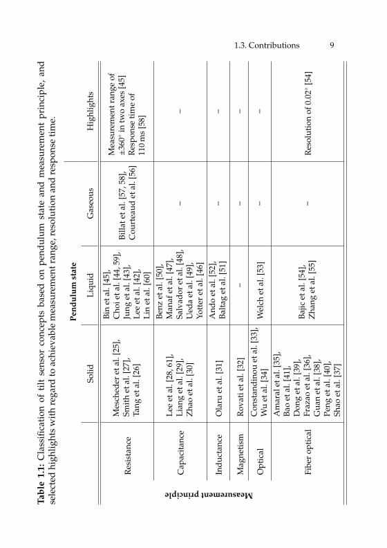
1.3. Contributions 9T
ab
le1
.1:
Cla
ssifi
cati
onof
tilt
sen
sor
con
cep
tsba
sed
onp
end
ulu
mst
ate
and
mea
sure
men
tp
rin
cip
le,
and
sele
cted
hig
hli
ghts
wit
hre
gard
toac
hie
vabl
em
easu
rem
ent
ran
ge,r
esol
uti
onan
dre
spon
seti
me.
Pe
nd
ulu
mst
ate
Soli
dL
iqu
idG
aseo
us
Hig
hli
ghts
Measurementprinciple
Res
ista
nce
Mes
ched
eret
al.[
25],
Smit
het
al.[
27],
Tan
get
al.[
26]
Bin
etal
.[45
],C
hoi
etal
.[44
,59]
,Ju
ng
etal
.[43
],L
eeet
al.[
42],
Lin
etal
.[60
]
Bil
lat
etal
.[57
,58]
,C
ourt
eau
det
al.[
56]
Mea
sure
men
tra
nge
of±3
60
intw
oax
es[4
5]R
esp
onse
tim
eof
110
ms
[58]
Cap
acit
ance
Lee
etal
.[28
,61]
,L
ian
get
al.[
29],
Zh
aoet
al.[
30]
Ben
zet
al.[
50],
Man
afet
al.[
47],
Salv
ador
etal
.[48
],U
eda
etal
.[49
],Yo
tter
etal
.[46
]
––
Ind
uct
ance
Ola
ruet
al.[
31]
An
do
etal
.[52
],B
alta
get
al.[
51]
––
Mag
net
ism
Rov
atie
tal
.[32
]–
––
Op
tica
lC
onst
and
inou
etal
.[33
],W
uet
al.[
34]
Wel
chet
al.[
53]
––
Fibe
rop
tica
l
Am
aral
etal
.[35
],B
aoet
al.[
41],
Don
get
al.[
39],
Fraz
aoet
al.[
36],
Gu
anet
al.[
38],
Pen
get
al.[
40],
Shao
etal
.[37
]
Baj
icet
al.[
54],
Zh
ang
etal
.[55
]–
Res
olu
tion
of0.
02
[54]
10 Chapter 1: Introduction
Tilt switch Tilt sensor
Chap. 3: Pendulum
Chap. 5: Contact mechanics
Chap. 6: Sensor modeling
Technologyand materials
Chap. 7: Evaluation
Chap. 4: Cavity
Chap. 2: Sensor system
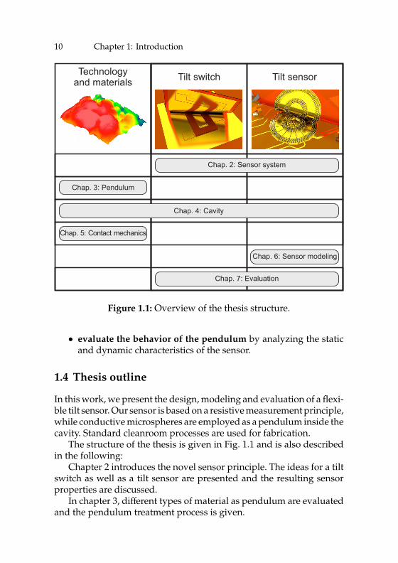
Figure 1.1: Overview of the thesis structure.
• evaluate the behavior of the pendulum by analyzing the staticand dynamic characteristics of the sensor.
1.4 Thesis outline
In this work, we present the design, modeling and evaluation of a flexi-ble tilt sensor. Our sensor is based on a resistive measurement principle,while conductive microspheres are employed as a pendulum inside thecavity. Standard cleanroom processes are used for fabrication.
The structure of the thesis is given in Fig. 1.1 and is also describedin the following:
Chapter 2 introduces the novel sensor principle. The ideas for a tiltswitch as well as a tilt sensor are presented and the resulting sensorproperties are discussed.
In chapter 3, different types of material as pendulum are evaluatedand the pendulum treatment process is given.
1.5. Publications 11
Chapter 4 covers the fabrication process of the sensor cavity and thewhole sensing structure for two different approaches. The bendabilityof both approaches is also evaluated.
The effects of the electrical contact between contact pad and pendu-lum are examined in chapter 5 and the surface roughness with regardto friction and adhesion is analyzed.
The important design parameters for the tilt sensor are evaluatedin chapter 6 by creating an analytical model of the sensor. The optimalparameters with respect to the sensor requirements are defined.
The tilt switch and tilt sensor are characterized in chapter 7. First astatic evaluation is performed, followed by an analysis of the dynamicmicrosphere movement in the cavity of the tilt sensor.
Chapter 8 summarizes the findings from this thesis and providesan outlook on further work and possible applications.
1.5 Publications
This thesis is based on the following publications:
• L. Büthe, C. Vogt, L. Petti, G. Cantarella, N. Münzenrieder andG. Tröster. Fabrication, modeling and evaluation of a digital out-put tilt sensor with conductive microspheres. In IEEE SensorsJournal, 2017, submitted.
• L. Büthe, C. Vogt, L. Petti, G. Cantarella, N. Münzenrieder andG. Tröster. Digital output flexible tilt sensor with conductive mi-crospheres. In Proceedings of the IEEE Sensors 2015, pages 1–4,2015.
• L. Büthe, C. Vogt, L. Petti, N. Münzenrieder, C. Zysset, G. Sal-vatore and G. Tröster. A Mechanically Flexible Tilt Switch OnKapton Foil With Microspheres As A Pendulum. In Proceedingsof Sensors and Measuring Systems 2014; 17. ITG/GMA Symposium,pages 1–4, 2014.
The following publications have been authored and co-authoredadditionally:
• L. Büthe, O. Amft, G. Tröster. Textile-integrated sensor technolo-gies for posture and movement detection. In Context-Aware Sys-tems - Fundamentals and Applications. Lecture Notes in ComputerScience, submitted.
12 Chapter 1: Introduction
• L. Büthe, U. Blanke, H. Capkevics, G. Tröster. A wearable sensingsystem for timing analysis in tennis. In Proceedings of the 2016IEEE 13th International Conference on Wearable and Implantable BodySensor Networks (BSN), pages 43–48, 2016.
• N. Münzenrieder, D. Karnaushenko, L. Petti, G. Cantarella,C. Vogt, L. Büthe, D. D. Karnaushenko, O. G. Schmidt,D. Makarov and G. Tröster. Entirely Flexible On-Site ConditionedMagnetic Sensorics. In Advanced Electronic Materials, 2(8), page1600188, 2016.
• L. Petti, N. Münzenrieder, C. Vogt, H. Faber, L. Büthe,G. Cantarella, T. D. Anthopoulos and G. Tröster. Metal oxidesemiconductor thin-film transistors for flexible electronics, In Ap-plied Physics Review, 3(2), page 021303, 2016.
• G. Cantarella, N. Münzenrieder, L. Petti, C. Vogt, L. Büthe,G. A. Salvatore, A. Daus and G. Tröster. Flexible In-Ga-Zn-O Thin-Film Transistors on elastomeric substrate bent to 2.3%strain. In IEEE Electron Device Letters, 36(8), pages 781–783, 2015.
• L. Petti, A. Frutiger, N. Münzenrieder, G. A. Salvatore, L. Büthe,C. Vogt, G. Cantarella and G. Tröster. Flexible Quasi-Vertical In-Ga-Zn-O Thin-Film Transistor with 300 nm Channel Length. InIEEE Electron Device Letters, 36(5), pages 475–477, 2015.
• N. Münzenrieder, G. Cantarella, C. Vogt, L. Petti, L. Büthe,G. A. Salvatore, Y. Fang, R. Andri, Y. Lam, R. Libanori, D. Widner,A. Studart and G. Tröster. Stretchable and Conformable OxideThin-Film Electronics. In Advanced Electronic Materials, 1(3), page1400038, 2015.
• N. Münzenrieder, G. A. Salvatore, L. Petti, C. Zysset, L. Büthe,C. Vogt, G. Cantarella and G. Tröster. Contact resistance andoverlapping capacitance in flexible sub-micron long oxide thin-film transistors for above 100 MHz operation. In Applied PhysicsLetters, 105(26), page 263504, 2014.
• L. Petti, N. Münzenrieder, G. A. Salvatore, C. Zysset, T. Kinkeldei,L. Büthe, C. Vogt and G. Tröster. Flexible electronics based on ox-ide semiconductors. In 2014 21st International Workshop on Active-Matrix Flatpanel Displays and Devices (AM-FPD), pages 323–326,2014.
1.5. Publications 13
• N. Münzenrieder, P. Voser, L. Petti, C. Zysset, L. Büthe, C. Vogt,G. A. Salvatore and G. Tröster. Flexible Self-Aligned Double-GateIGZO TFT. In IEEE Electron Device Letters, 35(1), pages 69–71,2014.
• L. Petti, N. Münzenrieder, G. A. Salvatore, C. Zysset, T. Kinkeldei,L. Büthe and G. Tröster. Influence of Mechanical Bending on Flex-ible InGaZnO-Based Ferroelectric Memory TFTs. In IEEE Trans-actions on Electron Devices, 61(4), pages 1085–1092.
• L. Petti, F. Bottacchi, N. Münzenrieder, H. Faber, G. Cantarella,C. Vogt, L. Büthe, I. Namal, F. Spath, T. Hertel, T. D. Anthopoulosand G. Tröster. Integration of solution-processed (7,5) SWCNTswith sputtered and spray-coated metal oxides for flexible com-plementary inverters. In 2014 IEEE International Electron DevicesMeeting (IEDM). pages 610–613, 2014.
• L. Büthe, M. Hardegger, P. Brülisauer and G. Tröster. RFID-Die:Battery-free Orientation Sensing Using an Array of Passive TiltSwitches. In Proceedings of the 2014 ACM International Joint Con-ference on Pervasive and Ubiquitous Computing: Adjunct Publication,pages 215–218, 2014.
• G. A. Salvatore, N. Münzenrieder, T. Kinkeldei, L. Petti, C. Zys-set, I. Strebel, L. Büthe and G. Tröster. Wafer-scale design oflightweight and transparent electronics that wraps around hair.In Nature Communications, 5(2982), pages 1–8, 2014.
• G. A. Salvatore, N. Münzenrieder, C. Barraud, L. Petti, C. Zysset,L. Büthe, K. Ensslin and G. Tröster. Fabrication and Transfer ofFlexible Few-Layers MoS2 Thin Film Transistors to Any Arbi-trary Substrate. In ACS Nano, 7(10), pages 8809–8815, 2013.
• C. Zysset, N. Münzenrieder, L. Petti, L. Büthe, G. A. Salvatore andG. Tröster. IGZO TFT-Based All-Enhancement Operational Am-plifier Bent to a Radius of 5 mm. In IEEE Electron Device Letters,34(11), pages 1394–1396, 2013.
• N. Münzenrieder, G. A. Salvatore, T. Kinkeldei, L. Petti, C. Zys-set, L. Büthe and G. Tröster. InGaZnO TFTs on a Flexible Mem-brane Transferred to a Curved Surface with a Radius of 2 mm. In2013 71st Annual Device Research Conference (DRC), pages 165–166,2013.
14 Chapter 1: Introduction
• N. Münzenrieder, L. Petti, C. Zysset, D. Görk, L. Büthe, G. A. Sal-vatore and G. Tröster. Investigation of gate material ductilityenables flexible a-IGZO TFTs bendable to a radius of 1.7 mm. In43rd European Solid-State Device Research Conference (ESSDERC13),pages 362–365, 2013.
• L. Petti, P. Aguirre, N. Münzenrieder, G. A. Salvatore, C. Zysset,A. Frutiger, L. Büthe, C. Vogt and G. Tröster. Mechanically flexiblevertically integrated a-IGZO thin-film transistors with 500 nmchannel length fabricated on free standing plastic foil. In 2013IEEE International Electron Devices Meeting (IEDM), pages 296–299, 2013.
• C. Zysset, N. Nasseri, L. Büthe, N. Münzenrieder, T. Kinkeldei,L. Petti, S. Kleiser, G. A. Salvatore, M. Wolf and G. Tröster. Textileintegrated sensors and actuators for near-infrared spectroscopy.In Optics Express, 21(3), pages 3213–3224, 2013.
• S. Jalaliniya, J. Smith, M. Sousa, L. Büthe and T. Pederson. Touch-less Interaction with Medical Images Using Hand & Foot Ges-tures. In Proceedings of the 2013 ACM Conference on Pervasive andUbiquitous Computing: Adjunct Publication, pages 1265–1274, 2013.
2Sensor system
We introduce the general sensing principle. Two different design architecturesare described which will be evaluated in more detail in the following chapters.Finally, the sensor properties which are achievable with the architectures arereported.
16 Chapter 2: Sensor system
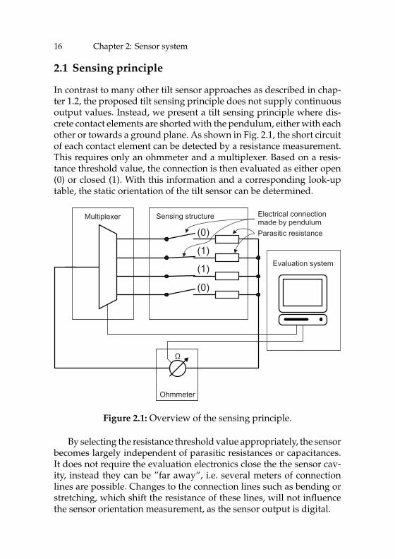
2.1 Sensing principle
In contrast to many other tilt sensor approaches as described in chap-ter 1.2, the proposed tilt sensing principle does not supply continuousoutput values. Instead, we present a tilt sensing principle where dis-crete contact elements are shorted with the pendulum, either with eachother or towards a ground plane. As shown in Fig. 2.1, the short circuitof each contact element can be detected by a resistance measurement.This requires only an ohmmeter and a multiplexer. Based on a resis-tance threshold value, the connection is then evaluated as either open(0) or closed (1). With this information and a corresponding look-uptable, the static orientation of the tilt sensor can be determined.
(0)
(1)
(1)
(0)
Multiplexer Sensing structure
Ω
Ohmmeter
Evaluation system
Electrical connectionmade by pendulumParasitic resistance
Figure 2.1: Overview of the sensing principle.
By selecting the resistance threshold value appropriately, the sensorbecomes largely independent of parasitic resistances or capacitances.It does not require the evaluation electronics close the the sensor cav-ity, instead they can be ”far away”, i.e. several meters of connectionlines are possible. Changes to the connection lines such as bending orstretching, which shift the resistance of these lines, will not influencethe sensor orientation measurement, as the sensor output is digital.
2.2. Design and architecture 17
2.2 Design and architecture
Based on the previously described sensing principle, we propose twodifferent types of tilt sensing architectures:
• Tilt switch: A tilt switch is a switch with two states, i.e. openwhen tilted in one direction with respect to horizontal, and closedwhen tilted in the other direction.
• Tilt sensor: The tilt sensor measures the tilt of the device with acertain angular resolution.
As a pendulum conductive microspheres are used which will be dis-cussed in more detail in chapter 3. Both sensing architectures havetheir advantages and disadvantages, especially with regard to resolu-tion and complexity, and will be discussed in the following sections.
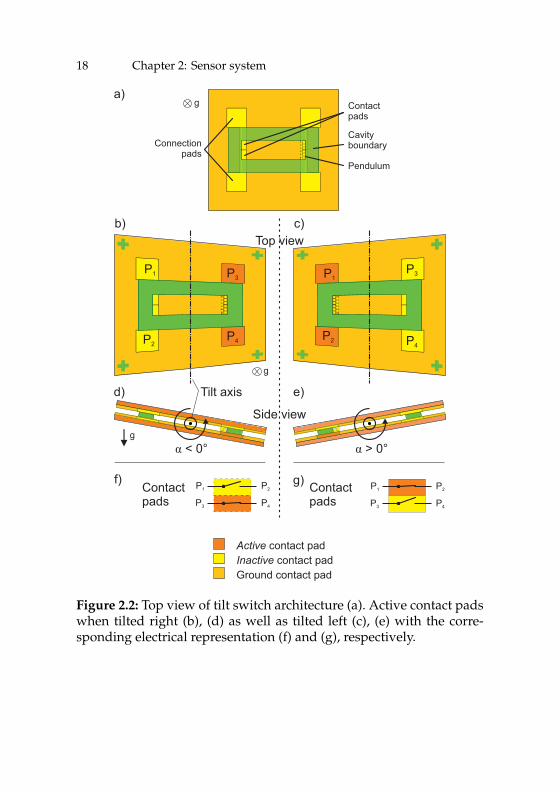
2.2.1 Tilt switch
The schematic design of the tilt switch is shown in Fig. 2.2. On eachside of the cavity two contact pads are located. The pendulum insidethe cavity boundaries follows the orientation of gravity and connectstwo adjacent contact pads. This indicates the orientation of the device,i.e. whether the sensor is tilted to the right side (Fig. 2.2b, d) or to theleft side (Fig. 2.2c, e). The state of two contact pads is either active whenthey are connected by the pendulum or inactive when no electrical con-nection is made. By evaluating this state, the electrical representationof the sensor (Fig. 2.2f, g) and subsequently its orientation can be deter-mined. The rectangular shape of the cavity ensures that the pendulumcan only lie at the end of the cavity where the contact pads are located.
The tilt switch can only detect tilt changes along the axis as indicatedin Fig. 2.2b. Other tilt of the sensor cannot reliably be detected by theproposed concept.
In case the sensor is held horizontally, the microspheres can spreadat random over the area of the cavity. Thus, designing the sensor withcontact pads on either side of the cavity, this state can be detected aswell as both contacts on either side will not be in electrical contact.
This architecture is especially useful in scenarios where only knowl-edge about the direction of tilt of the device is required.
18 Chapter 2: Sensor system
Active contact padInactive contact padGround contact pad
Connectionpads
Cavityboundary
P2
P1 P3
P4
Tilt axis
b)
d)
P2
P1P3
P4
c)
e)
Contactpads
f) P1 P2
P3 P4
P1 P2
P3 P4
Contactpads
g)
Top view
Side view
a)
Pendulum
Contactpads
g
g
gα < 0° α > 0°
Figure 2.2: Top view of tilt switch architecture (a). Active contact padswhen tilted right (b), (d) as well as tilted left (c), (e) with the corre-sponding electrical representation (f) and (g), respectively.
2.2. Design and architecture 19
2.2.2 Tilt sensor1
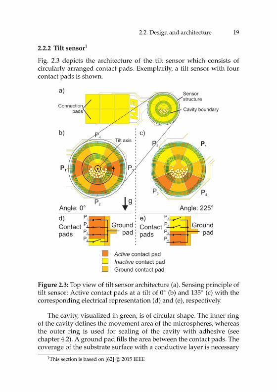
Fig. 2.3 depicts the architecture of the tilt sensor which consists ofcircularly arranged contact pads. Exemplarily, a tilt sensor with fourcontact pads is shown.
Active contact padInactive contact padGround contact pad
a) Sensorstructure
Connectionpads
Angle: 0°g
b)
P1
P2
P3
P4
Angle: 225°
c)
P1P2
P3 P4
Groundpad
Contactpads
d) P1
P2
P3
P4
Groundpad
Contactpads
e) P1
P2
P3
P4
Cavity boundary
Tilt axis
Figure 2.3: Top view of tilt sensor architecture (a). Sensing principle oftilt sensor: Active contact pads at a tilt of 0 (b) and 135 (c) with thecorresponding electrical representation (d) and (e), respectively.
The cavity, visualized in green, is of circular shape. The inner ringof the cavity defines the movement area of the microspheres, whereasthe outer ring is used for sealing of the cavity with adhesive (seechapter 4.2). A ground pad fills the area between the contact pads. Thecoverage of the substrate surface with a conductive layer is necessary
1This section is based on [62] c© 2015 IEEE
20 Chapter 2: Sensor system
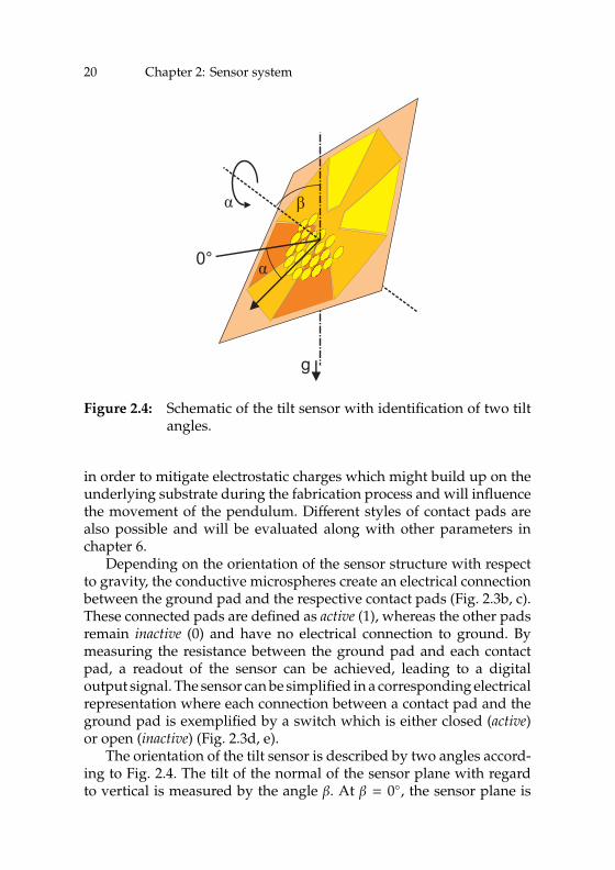
0° α
β
g
α
Figure 2.4: Schematic of the tilt sensor with identification of two tiltangles.
in order to mitigate electrostatic charges which might build up on theunderlying substrate during the fabrication process and will influencethe movement of the pendulum. Different styles of contact pads arealso possible and will be evaluated along with other parameters inchapter 6.
Depending on the orientation of the sensor structure with respectto gravity, the conductive microspheres create an electrical connectionbetween the ground pad and the respective contact pads (Fig. 2.3b, c).These connected pads are defined as active (1), whereas the other padsremain inactive (0) and have no electrical connection to ground. Bymeasuring the resistance between the ground pad and each contactpad, a readout of the sensor can be achieved, leading to a digitaloutput signal. The sensor can be simplified in a corresponding electricalrepresentation where each connection between a contact pad and theground pad is exemplified by a switch which is either closed (active)or open (inactive) (Fig. 2.3d, e).
The orientation of the tilt sensor is described by two angles accord-ing to Fig. 2.4. The tilt of the normal of the sensor plane with regardto vertical is measured by the angle β. At β = 0, the sensor plane is
2.2. Design and architecture 21
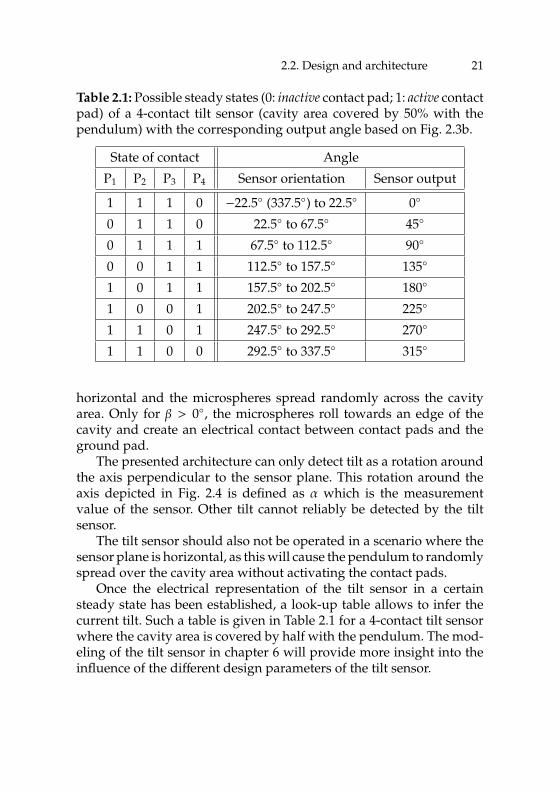
Table 2.1: Possible steady states (0: inactive contact pad; 1: active contactpad) of a 4-contact tilt sensor (cavity area covered by 50% with thependulum) with the corresponding output angle based on Fig. 2.3b.
State of contact Angle
P1 P2 P3 P4 Sensor orientation Sensor output
1 1 1 0 −22.5 (337.5) to 22.5 0
0 1 1 0 22.5 to 67.5 45
0 1 1 1 67.5 to 112.5 90
0 0 1 1 112.5 to 157.5 135
1 0 1 1 157.5 to 202.5 180
1 0 0 1 202.5 to 247.5 225
1 1 0 1 247.5 to 292.5 270
1 1 0 0 292.5 to 337.5 315
horizontal and the microspheres spread randomly across the cavityarea. Only for β > 0, the microspheres roll towards an edge of thecavity and create an electrical contact between contact pads and theground pad.
The presented architecture can only detect tilt as a rotation aroundthe axis perpendicular to the sensor plane. This rotation around theaxis depicted in Fig. 2.4 is defined as α which is the measurementvalue of the sensor. Other tilt cannot reliably be detected by the tiltsensor.
The tilt sensor should also not be operated in a scenario where thesensor plane is horizontal, as this will cause the pendulum to randomlyspread over the cavity area without activating the contact pads.
Once the electrical representation of the tilt sensor in a certainsteady state has been established, a look-up table allows to infer thecurrent tilt. Such a table is given in Table 2.1 for a 4-contact tilt sensorwhere the cavity area is covered by half with the pendulum. The mod-eling of the tilt sensor in chapter 6 will provide more insight into theinfluence of the different design parameters of the tilt sensor.
22 Chapter 2: Sensor system
2.3 Sensor properties
With the previously described tilt sensing designs, several sensor prop-erties can be achieved:
• Mechanical properties and dimensions
As the tilt sensor is intended for use in wearable devices, thesensor should be bendable without losing its functionality. Wewill demonstrate the bendability in chapter 4 while chapter 7examines the functionality after bending of the device.
The proposed concepts allow the fabrication of a flat sensor wherethe thickness of the device is limited by the diameter of the micro-spheres which are used as the pendulum. Chapter 4 will demon-strate that this allows to build sensors that do not exceed thedimensions of current state-of-the-art MEMS tilt sensors whichhave a diameter of around 5 mm including the packaging.
• Sensor readout
The sensing principle enables a sensor readout that does notrequire sophisticated electronics, such as amplifiers, etc. close tothe sensor. Instead the readout electronics can be located at acentral distant location within a smart textile [63] while parasiticinfluences, e.g from the connection lines, do not influence thedigital output signal.
• Materials and technology
In chapter 4 we will show the fabrication of the sensors on free-standing foil. Therefore we enable the assembly of devices suchas electronics [64] or sensors [65] in one process flow with the tiltsensor. This would allow the integration of several other sensors,such as strain or temperature sensors, or even small circuits [66]to create smart sensor nodes on plastic.
2.4 Conclusion
Two different architectures based on the proposed tilt sensing principlehave been presented with their basic operating principle. A tilt switchcan detect the orientation of the tilt without allowing to infer the tiltangle. To gain insight into the applied tilt angle, the second approach

2.4. Conclusion 23
for a tilt sensor needs to be applied. This architecture will be modeledin chapter 6.


3Pendulum
The material choice of the pendulum is discussed and several options arecompared. We select solder spheres as the final choice for the pendulum anddescribe how the surface conductivity is increased by coating with gold.
26 Chapter 3: Pendulum
3.1 Material selection
The pendulum is the part of the sensor which follows the direction ofgravity inside the cavity and creates a change in the output signal ofthe sensor. Although the sensing principle in the previous chapter 2 isexplained with the use of solid microspheres, different types of mate-rials are possible for the proposed system. In general solids in the formof microspheres as well as liquids are qualified for this, while gaseouselements are discarded as they would not be able to create an electricalconnection.
A solid or liquid pendulum also needs to fulfill the following crite-ria to be suitable for our tilt sensor:
• Conductivity: The material should be electrically conductive, i.e.resulting in a resistance in the range of kΩ or less so that theelectrical connection between the contact pads can be clearlyidentified.
• Density: A larger density of the used material ensures that thegravitational field dominates the movement of the pendulumcompared to other parasitic forces.
In addition, liquids have also additional requirements to conformwith:
• Surface tension: The surface tension γlv of the liquids should behigh to ensure a high contact angle θwhich is represented by thefollowing relation: cos(θ) ∼ −γlv. This results in a low wetting onthe substrate surface which is desirable to keep the contact areasmall and have low adhesion forces between the pendulum andthe substrate (see chapter 5).
• Vapor pressure: The vapor pressure which is an indicator for aliquid’s evaporation rate should be preferably low. This ensuresthat the material inside the cavity does not convert to the gaseousphase.
• Viscosity: The viscosity of the liquid, a measure of the resistanceto deformation, should be low to ensure a good response time ofthe sensor.
A solid pendulum needs to show a high uniformity and roundnessof the microspheres to ensure a free pendulum movement inside thecavity.
3.1. Material selection 27
3.1.1 Liquids
As liquids, we have identified ionic liquids (IL) as the most promisingcategory. IL are salts in a liquid state. Usually salts, such as NaCl, havehigh melting temperatures high above room temperature, but therealso exist salts which are liquid at room temperature and are now inthe focus of various research areas [67, 68, 69]. As they contain ions,they are electrically conductive and have been used as conductingfluids for different applications [70, 71]. They also exhibit a low vaporpressure [72, 73] as a consequence of their ionic nature.
The sensor design requires the pendulum to create an electricalconnection between different areas on the substrate surface, i.e. thecontact pads and the ground pad. This requires the pendulum to haveseveral contact points with the substrate surface. A liquid pendulumthat consists of several, individual spherically shaped elements wouldunite to a single, larger element. This single pendulum would have acontact area with the substrate surface which covers the contact padsand ground pad, compared to several, small contact points of eachpendulum element. The contact area leads to increased adhesion forcesof the pendulum with the substrate which decrease the performanceof the sensor.
In addition, the design of the sensor aims for a height of the cavitywhich is less than 1 mm, a domain where the capillary effect has aninfluence on a liquid pendulum. The height h of a liquid column withthe density ρl in a tube with the radius r is given as [74]
h =2γlvcos(θ)ρlgr
. (3.1)
A reduced height of the cavity which relates to a reduced tube radius rleads to an increased capillary height h which indicates high capillaryforces. These capillary forces which act against the gravitational forcesinfluence the movement of the pendulum inside the cavity.
The surface tension also has an influence on the response time.Bin et al. [45] demonstrate that a reduction of the cavity size from10 mm to 6 mm increases the response time from 0.17 s to 0.65 s whichis caused by the liquid’s surface tension. The response time, a measurefor the time from when a tilt is applied until the correct output signal isachieved, should be minimal to allow a fast adaptation of the tilt sensorto new input angle values. The viscosity of IL is also larger than otherelectrically conductive liquids [75], thus rendering IL not suitable forachieving a low response time of the tilt sensor.
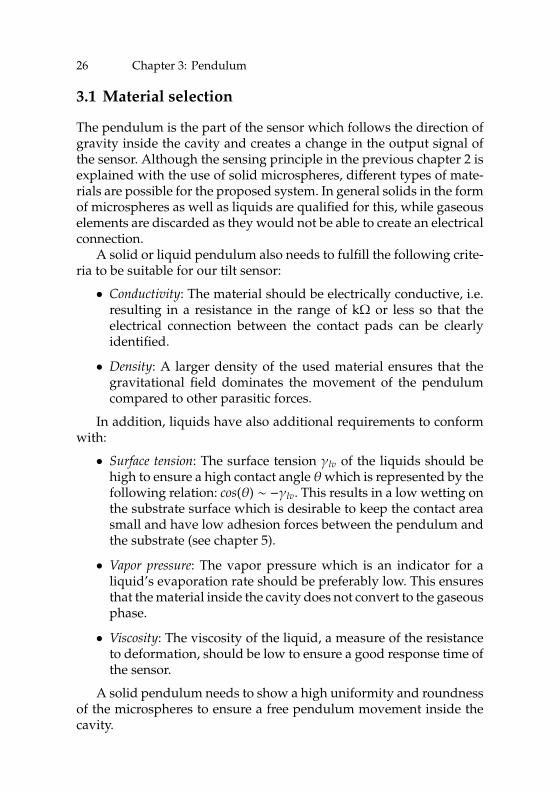
28 Chapter 3: Pendulum
1 mm
(a)
1 mm
(b)
1 mm
(c)
1 mm
(d)
Figure 3.1: Microscope images of different spheres: (a) Hollow glassspheres coated with silver; (b) Cast steel; (c) Tin-bronze alloy; (d) Tin-silver-copper solder spheres.
Based on the previously listed requirements, we conclude that ionicliquids are not appropriate for the use as pendulum in the proposedtilt sensor.
3.1.2 Solids
A solid pendulum can either consist of a solid conductive material or ofnon-conductive spheres which are coated with a conductive material.Examples for the former are hollow glass microspheres coated withsilver [76] as they are used in conductive paint (Fig. 3.1a). However,these hollow spheres have a density of only 0.16 g cm−3.
The alternative is to use a single solid material as pendulum. Micro-spheres such as spheres from cast steel used for shot blasting [77] varysignificantly in size and also do not exhibit a good roundness (Fig. 3.1b).However, a homogeneous size and good roundness are crucial for arepeatable movement of the pendulum in the cavity. These observa-
3.1. Material selection 29
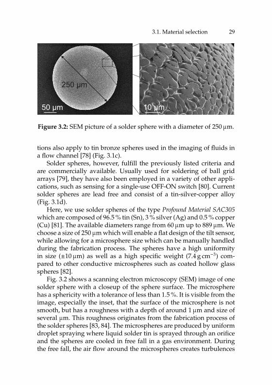
10 µm50 µm
250 µm
Figure 3.2: SEM picture of a solder sphere with a diameter of 250µm.
tions also apply to tin bronze spheres used in the imaging of fluids ina flow channel [78] (Fig. 3.1c).
Solder spheres, however, fulfill the previously listed criteria andare commercially available. Usually used for soldering of ball gridarrays [79], they have also been employed in a variety of other appli-cations, such as sensing for a single-use OFF-ON switch [80]. Currentsolder spheres are lead free and consist of a tin-silver-copper alloy(Fig. 3.1d).
Here, we use solder spheres of the type Profound Material SAC305which are composed of 96.5 % tin (Sn), 3 % silver (Ag) and 0.5 % copper(Cu) [81]. The available diameters range from 60µm up to 889µm. Wechoose a size of 250µm which will enable a flat design of the tilt sensor,while allowing for a microsphere size which can be manually handledduring the fabrication process. The spheres have a high uniformityin size (±10µm) as well as a high specific weight (7.4 g cm−3) com-pared to other conductive microspheres such as coated hollow glassspheres [82].
Fig. 3.2 shows a scanning electron microscopy (SEM) image of onesolder sphere with a closeup of the sphere surface. The microspherehas a sphericity with a tolerance of less than 1.5 %. It is visible from theimage, especially the inset, that the surface of the microsphere is notsmooth, but has a roughness with a depth of around 1µm and size ofseveral µm. This roughness originates from the fabrication process ofthe solder spheres [83, 84]. The microspheres are produced by uniformdroplet spraying where liquid solder tin is sprayed through an orificeand the spheres are cooled in free fall in a gas environment. Duringthe free fall, the air flow around the microspheres creates turbulences
30 Chapter 3: Pendulum
Microspheres Loudspeakermembrane
Batteries Controlelectronics
(a)
TargetPlasma
Vacuumchamber
Microspheres Loudspeakermembrane
(b)
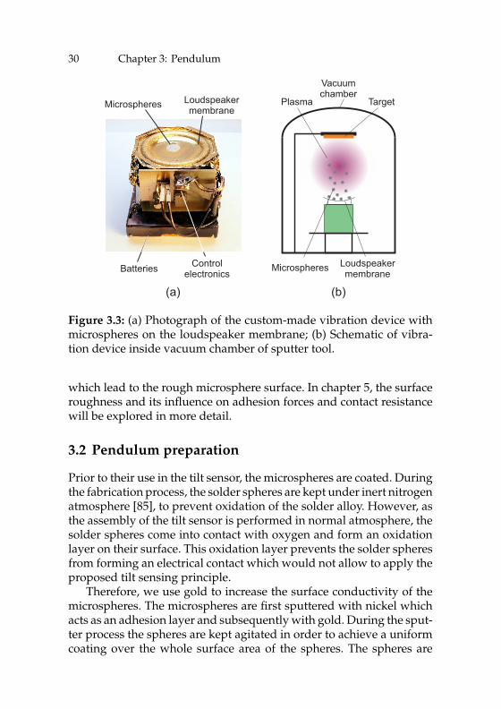
Figure 3.3: (a) Photograph of the custom-made vibration device withmicrospheres on the loudspeaker membrane; (b) Schematic of vibra-tion device inside vacuum chamber of sputter tool.
which lead to the rough microsphere surface. In chapter 5, the surfaceroughness and its influence on adhesion forces and contact resistancewill be explored in more detail.
3.2 Pendulum preparation
Prior to their use in the tilt sensor, the microspheres are coated. Duringthe fabrication process, the solder spheres are kept under inert nitrogenatmosphere [85], to prevent oxidation of the solder alloy. However, asthe assembly of the tilt sensor is performed in normal atmosphere, thesolder spheres come into contact with oxygen and form an oxidationlayer on their surface. This oxidation layer prevents the solder spheresfrom forming an electrical contact which would not allow to apply theproposed tilt sensing principle.
Therefore, we use gold to increase the surface conductivity of themicrospheres. The microspheres are first sputtered with nickel whichacts as an adhesion layer and subsequently with gold. During the sput-ter process the spheres are kept agitated in order to achieve a uniformcoating over the whole surface area of the spheres. The spheres are
3.3. Conclusion 31
placed on a loudspeaker membrane which acts as a vibration deviceas shown in Fig. 3.3a and is oscillating at a frequency of 150 Hz, keep-ing the spheres agitated during the sputter process. A battery supplyallows the operation of the device inside the sputter vacuum cham-ber (Fig. 3.3b). We deposit nickel at a rate of 1 nm/min for 2 min andgold at a rate of 16 nm/min for 4 min, achieving coating thicknesses of3 nm and 16 nm, respectively. In chapter 5, we evaluate the resultingresistance of the coated microsphere with the substrate surface.
3.3 Conclusion
We introduced the requirements for the pendulum, followed by a dis-cussion on different pendulum materials. Liquids are not a suitable ma-terial for a pendulum, solids are advantageous. Several sphere typeswere evaluated, but could not be considered due to the lack of homo-geneity over all spheres and the sphericity of a single sphere. Solderspheres are selected as the best choice as a pendulum and coated uni-formly to mitigate surface oxidation.


4Cavity
We present two different fabrication processes for the cavity and the completetilt switch and tilt sensor. Both approaches are compared with each other andevaluated for the bendability of the cavity.
34 Chapter 4: Cavity
The cavity defines the boundaries of the volume in which the pen-dulum can move freely across the contact pads. In addition, the cavityhas to enable the bendability of the sensor without hindering the pen-dulum in its movement inside the cavity. As the sensor is fabricated onpolyimide foil, the processing temperatures should not exceed 200 C.
As possible applications (see chapter 8.4.2) require not only regularshaped cavities such as square or round, but also other cavity shapes,the fabrication process should allow for these designs. With photolitho-graphic processing arbitrary layouts of cavity can be imagined whilealso allowing for high resolution in the µm-range.
Metz et al. present the fabrication of flexible cavities with the use ofpolyimide as well as SU-8 [86, 87]. Based on this, we will present twodifferent approaches for fabrication of a flexible cavity, differing in theway how the side walls are created:
1. Stacking of polyimide layers: Layers of polyimide are structuredand then stacked upon each other to reach the desired thickness.
2. SU-8 pillars: Pillars of SU-8 define the layout of the cavity.
The following sections will present the fabrication steps and discussthe bendability with a focus on the second approach with SU-8 pillars.
4.1 Stacking of polyimide layers1
For this approach, several structured layers of polyimide foil arestacked upon each other forming the cavity. This allows to tailor theheight of the cavity in multiples of the polyimide foil thickness. Here,we use Kapton E (DuPont) with a thickness of 50µm.
4.1.1 Fabrication process
The fabrication process is shown in Fig. 4.1. First, e-beam evaporationis used to deposit 10 nm of chrome (Cr) and 60 nm of gold (Au) onthe polyimide foil (Fig. 4.1a). The chrome acts as an adhesion layerbetween the polyimide and the gold layer. Gold is used as electrodematerial as it is conductive without oxidizing. Both metal layers are
1This section is based on "‘Sensoren und Messsysteme 2014, ITG-Fachbericht 250,Beiträge der 17. ITG/GMA-Fachtagung vom 3. bis 4. Juni 2014, Beitrag 36: L. Büthe u.a.,A Mechanically Flexible Tilt Switch on Kapton Foil with Microspheres as a Pendulum"’,VDE VERLAG, Berlin, Offenbach, 2014. [88]
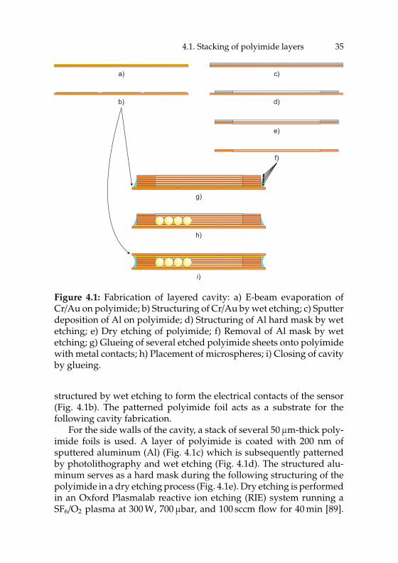
4.1. Stacking of polyimide layers 35
a)
b) d)
e)
f)
i)
g)
c)
h)
Figure 4.1: Fabrication of layered cavity: a) E-beam evaporation ofCr/Au on polyimide; b) Structuring of Cr/Au by wet etching; c) Sputterdeposition of Al on polyimide; d) Structuring of Al hard mask by wetetching; e) Dry etching of polyimide; f) Removal of Al mask by wetetching; g) Glueing of several etched polyimide sheets onto polyimidewith metal contacts; h) Placement of microspheres; i) Closing of cavityby glueing.
structured by wet etching to form the electrical contacts of the sensor(Fig. 4.1b). The patterned polyimide foil acts as a substrate for thefollowing cavity fabrication.
For the side walls of the cavity, a stack of several 50µm-thick poly-imide foils is used. A layer of polyimide is coated with 200 nm ofsputtered aluminum (Al) (Fig. 4.1c) which is subsequently patternedby photolithography and wet etching (Fig. 4.1d). The structured alu-minum serves as a hard mask during the following structuring of thepolyimide in a dry etching process (Fig. 4.1e). Dry etching is performedin an Oxford Plasmalab reactive ion etching (RIE) system running aSF6/O2 plasma at 300 W, 700µbar, and 100 sccm flow for 40 min [89].
36 Chapter 4: Cavity
Aluminum
Polyimide
20 µm
50 µm
15 µm
18°
Figure 4.2: SEM picture of the edge of a layer of polyimide coated withaluminum, structured with reactive ion etching. The sample is tiltedby 30.
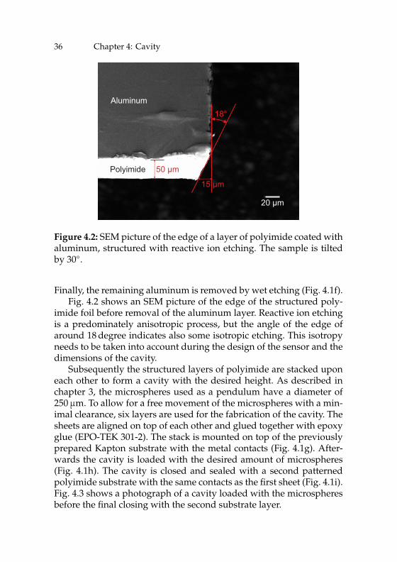
Finally, the remaining aluminum is removed by wet etching (Fig. 4.1f).Fig. 4.2 shows an SEM picture of the edge of the structured poly-
imide foil before removal of the aluminum layer. Reactive ion etchingis a predominately anisotropic process, but the angle of the edge ofaround 18 degree indicates also some isotropic etching. This isotropyneeds to be taken into account during the design of the sensor and thedimensions of the cavity.
Subsequently the structured layers of polyimide are stacked uponeach other to form a cavity with the desired height. As described inchapter 3, the microspheres used as a pendulum have a diameter of250µm. To allow for a free movement of the microspheres with a min-imal clearance, six layers are used for the fabrication of the cavity. Thesheets are aligned on top of each other and glued together with epoxyglue (EPO-TEK 301-2). The stack is mounted on top of the previouslyprepared Kapton substrate with the metal contacts (Fig. 4.1g). After-wards the cavity is loaded with the desired amount of microspheres(Fig. 4.1h). The cavity is closed and sealed with a second patternedpolyimide substrate with the same contacts as the first sheet (Fig. 4.1i).Fig. 4.3 shows a photograph of a cavity loaded with the microspheresbefore the final closing with the second substrate layer.
4.1. Stacking of polyimide layers 37
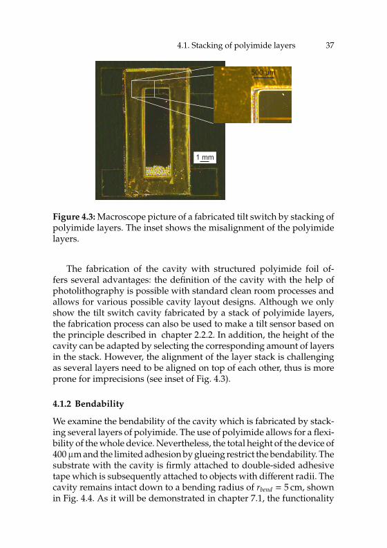
1 mm
500 µm
Figure 4.3: Macroscope picture of a fabricated tilt switch by stacking ofpolyimide layers. The inset shows the misalignment of the polyimidelayers.
The fabrication of the cavity with structured polyimide foil of-fers several advantages: the definition of the cavity with the help ofphotolithography is possible with standard clean room processes andallows for various possible cavity layout designs. Although we onlyshow the tilt switch cavity fabricated by a stack of polyimide layers,the fabrication process can also be used to make a tilt sensor based onthe principle described in chapter 2.2.2. In addition, the height of thecavity can be adapted by selecting the corresponding amount of layersin the stack. However, the alignment of the layer stack is challengingas several layers need to be aligned on top of each other, thus is moreprone for imprecisions (see inset of Fig. 4.3).
4.1.2 Bendability
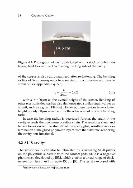
We examine the bendability of the cavity which is fabricated by stack-ing several layers of polyimide. The use of polyimide allows for a flexi-bility of the whole device. Nevertheless, the total height of the device of400µm and the limited adhesion by glueing restrict the bendability. Thesubstrate with the cavity is firmly attached to double-sided adhesivetape which is subsequently attached to objects with different radii. Thecavity remains intact down to a bending radius of rbend = 5 cm, shownin Fig. 4.4. As it will be demonstrated in chapter 7.1, the functionality
38 Chapter 4: Cavity
r = 5 cm
Figure 4.4: Photograph of cavity fabricated with a stack of polyimidelayers, bent to a radius of 5 cm along the long side of the cavity.
of the sensor is also still guaranteed after re-flattening. The bendingradius of 5 cm corresponds to a maximum compressive and tensilestrain of (see appendix, Eq. A.6)
ǫ =h
2rbend= 0.4% (4.1)
with h = 400µm as the overall height of the sensor. Bending ofother electronic devices has also demonstrated similar strain values asa limit, such as e.g. in TFTs [64]. However, these devices have a lowerheight of only 50µm which allows the achievement of lower bendingradii.
In case the bending radius is decreased further, the strain in thecavity exceeds the maximum possible strain. The resulting shear andtensile forces exceed the strength of the epoxy glue, resulting in a de-lamination of the glued polyimide layers from the substrate, renderingthe cavity non-functional.
4.2 SU-8 cavity2
The sensor cavity can also be fabricated by structuring SU-8 pillarson the polyimide substrate with the contact pads. SU-8 is a negativephotoresist, developed by IBM, which enables a broad range of thick-nesses from less than 1µm up to 450µm [90]. The resist is exposed with
2This section is based on [62] c© 2015 IEEE
4.2. SU-8 cavity 39
c)
d)
f)
g)
e)
b)
a)
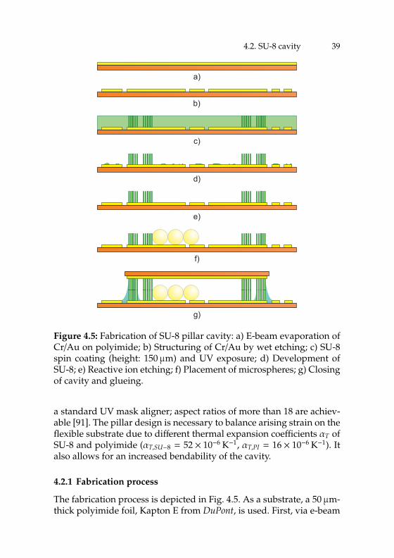
Figure 4.5: Fabrication of SU-8 pillar cavity: a) E-beam evaporation ofCr/Au on polyimide; b) Structuring of Cr/Au by wet etching; c) SU-8spin coating (height: 150µm) and UV exposure; d) Development ofSU-8; e) Reactive ion etching; f) Placement of microspheres; g) Closingof cavity and glueing.
a standard UV mask aligner; aspect ratios of more than 18 are achiev-able [91]. The pillar design is necessary to balance arising strain on theflexible substrate due to different thermal expansion coefficients αT ofSU-8 and polyimide (αT,SU−8 = 52 × 10−6 K−1, αT,PI = 16 × 10−6 K−1). Italso allows for an increased bendability of the cavity.
4.2.1 Fabrication process
The fabrication process is depicted in Fig. 4.5. As a substrate, a 50µm-thick polyimide foil, Kapton E from DuPont, is used. First, via e-beam
40 Chapter 4: Cavity
evaporation a layer of 10 nm of chrome is deposited, followed by 60 nmof gold. The chrome is an adhesion layer between the polyimide andthe gold layer while the gold layer itself acts as the conductive electrodematerial. The two metal layers are structured by wet etching and formthe contact pads of the sensor (Fig. 4.5a).
Subsequently, SU-8 2100 is spin coated with a thickness of 150µmonto the substrate and structured via photolithography with UV light(Fig. 4.5b). With mr-Dev 600, the SU-8 is developed, resulting in thedesired cavity structure (Fig. 4.5c). Reactive ion etching (RIE) with anO2-plasma is performed to remove remaining residue (Fig. 4.5d); thisis described in more detail in chapter 4.2.1.3. The resulting cavity isthen filled with the microspheres (Fig. 4.5e).
To close the cavity, a second sheet of polyimide foil with achrome/gold layer and SU-8 pillars is placed upside down on the topof the structure and finally sealed with epoxy glue (EPO-TEK 301-2)(Fig. 4.5f).
4.2.1.1 Pillar dimensions
The dimensions of the SU-8 pillars are evaluated to identify the idealedge length cpillar as well as spacing cdist for the given height of 150µmwith regard to bendability and fabrication yield.
• Pillar edge length: For a low stiffness and thus a high bendabilityof the sensor cavity, the edge length of the pillars should be assmall as possible. The bending stiffness is defined as the productof the Young’s Modulus E and the respective second moment ofarea I. The bending stiffness of polyimide foil with a thicknesshPI = 50µm and the Young’s Modulus EPI = 5.5 GPa, normalizedto its width w, is defined as
EPI ·IPI
w= EPI ·
wh3PI
12w= 5.73 × 10⁻⁵ N. (4.2)
For a polyimide foil coated with 150µm SU-8 and a Young’sModulus of ESU−8 = 4.95 GPa [92], the stiffness is at
ESU−8 ·Ipillar
w= ESU−8 ·
w (hPI + hSU−8)3
12w= 3.67 × 10⁻³ N. (4.3)
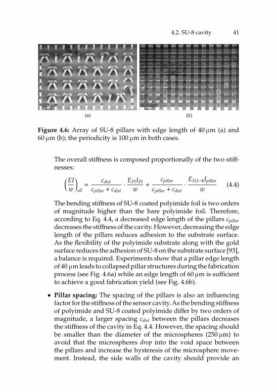
4.2. SU-8 cavity 41
100 µm 100 µm
(a) (b)
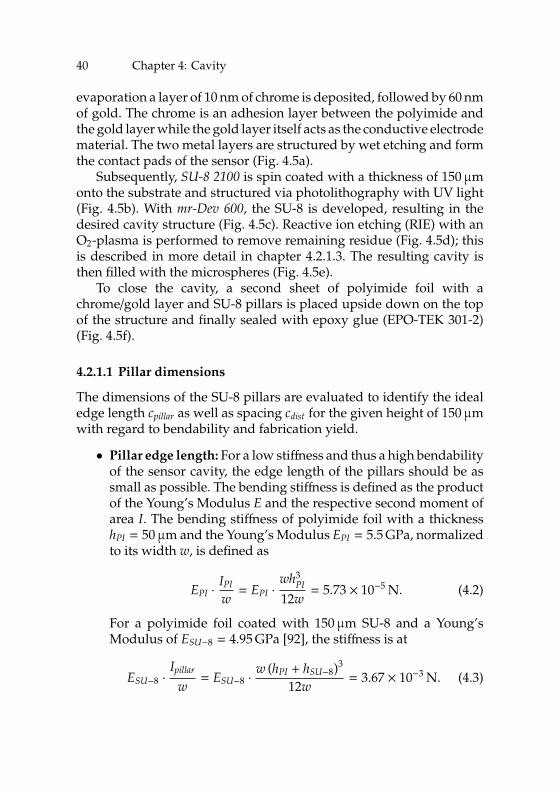
Figure 4.6: Array of SU-8 pillars with edge length of 40µm (a) and60µm (b); the periodicity is 100µm in both cases.
The overall stiffness is composed proportionally of the two stiff-nesses:
(
EI
w
)
all=
cdist
cpillar + cdist· EPIIPI
w+
cpillar
cpillar + cdist·
ESU−8Ipillar
w(4.4)
The bending stiffness of SU-8 coated polyimide foil is two ordersof magnitude higher than the bare polyimide foil. Therefore,according to Eq. 4.4, a decreased edge length of the pillars cpillar
decreases the stiffness of the cavity. However, decreasing the edgelength of the pillars reduces adhesion to the substrate surface.As the flexibility of the polyimide substrate along with the goldsurface reduces the adhesion of SU-8 on the substrate surface [93],a balance is required. Experiments show that a pillar edge lengthof 40µm leads to collapsed pillar structures during the fabricationprocess (see Fig. 4.6a) while an edge length of 60µm is sufficientto achieve a good fabrication yield (see Fig. 4.6b).
• Pillar spacing: The spacing of the pillars is also an influencingfactor for the stiffness of the sensor cavity. As the bending stiffnessof polyimide and SU-8 coated polyimide differ by two orders ofmagnitude, a larger spacing cdist between the pillars decreasesthe stiffness of the cavity in Eq. 4.4. However, the spacing shouldbe smaller than the diameter of the microspheres (250µm) toavoid that the microspheres drop into the void space betweenthe pillars and increase the hysteresis of the microsphere move-ment. Instead, the side walls of the cavity should provide an
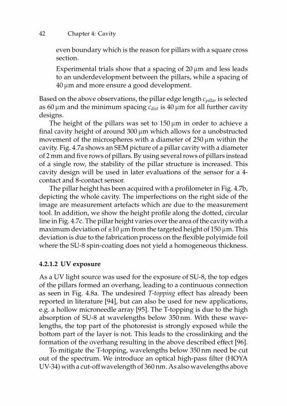
42 Chapter 4: Cavity
even boundary which is the reason for pillars with a square crosssection.
Experimental trials show that a spacing of 20µm and less leadsto an underdevelopment between the pillars, while a spacing of40µm and more ensure a good development.
Based on the above observations, the pillar edge length cpillar is selectedas 60µm and the minimum spacing cdist is 40µm for all further cavitydesigns.
The height of the pillars was set to 150µm in order to achieve afinal cavity height of around 300µm which allows for a unobstructedmovement of the microspheres with a diameter of 250µm within thecavity. Fig. 4.7a shows an SEM picture of a pillar cavity with a diameterof 2 mm and five rows of pillars. By using several rows of pillars insteadof a single row, the stability of the pillar structure is increased. Thiscavity design will be used in later evaluations of the sensor for a 4-contact and 8-contact sensor.
The pillar height has been acquired with a profilometer in Fig. 4.7b,depicting the whole cavity. The imperfections on the right side of theimage are measurement artefacts which are due to the measurementtool. In addition, we show the height profile along the dotted, circularline in Fig. 4.7c. The pillar height varies over the area of the cavity with amaximum deviation of±10µm from the targeted height of 150µm. Thisdeviation is due to the fabrication process on the flexible polyimide foilwhere the SU-8 spin-coating does not yield a homogeneous thickness.
4.2.1.2 UV exposure
As a UV light source was used for the exposure of SU-8, the top edgesof the pillars formed an overhang, leading to a continuous connectionas seen in Fig. 4.8a. The undesired T-topping effect has already beenreported in literature [94], but can also be used for new applications,e.g. a hollow microneedle array [95]. The T-topping is due to the highabsorption of SU-8 at wavelengths below 350 nm. With these wave-lengths, the top part of the photoresist is strongly exposed while thebottom part of the layer is not. This leads to the crosslinking and theformation of the overhang resulting in the above described effect [96].
To mitigate the T-topping, wavelengths below 350 nm need be cutout of the spectrum. We introduce an optical high-pass filter (HOYAUV-34) with a cut-offwavelength of 360 nm. As also wavelengths above
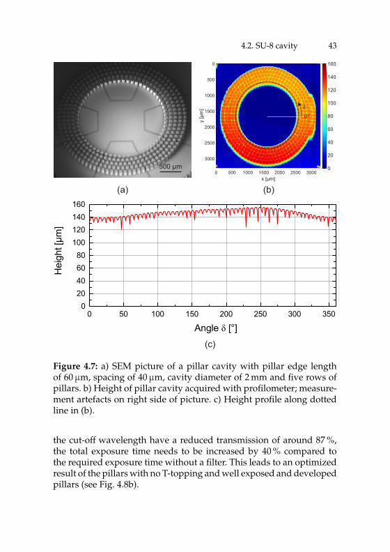
4.2. SU-8 cavity 43
(a) (b)
0 500 1000 1500 2000 2500 3000x [µm]
0
500
1000
1500
2000
2500
3000
y [µ
m]
0
20
40
60
80
100
120
140
160
0 50 100 150 200 250 300 3500
20406080
100120140160
Hei
ght [
µm]
Angle δ [°](c)
500 µm
δ
0°
Figure 4.7: a) SEM picture of a pillar cavity with pillar edge lengthof 60µm, spacing of 40µm, cavity diameter of 2 mm and five rows ofpillars. b) Height of pillar cavity acquired with profilometer; measure-ment artefacts on right side of picture. c) Height profile along dottedline in (b).
the cut-off wavelength have a reduced transmission of around 87 %,the total exposure time needs to be increased by 40 % compared tothe required exposure time without a filter. This leads to an optimizedresult of the pillars with no T-topping and well exposed and developedpillars (see Fig. 4.8b).
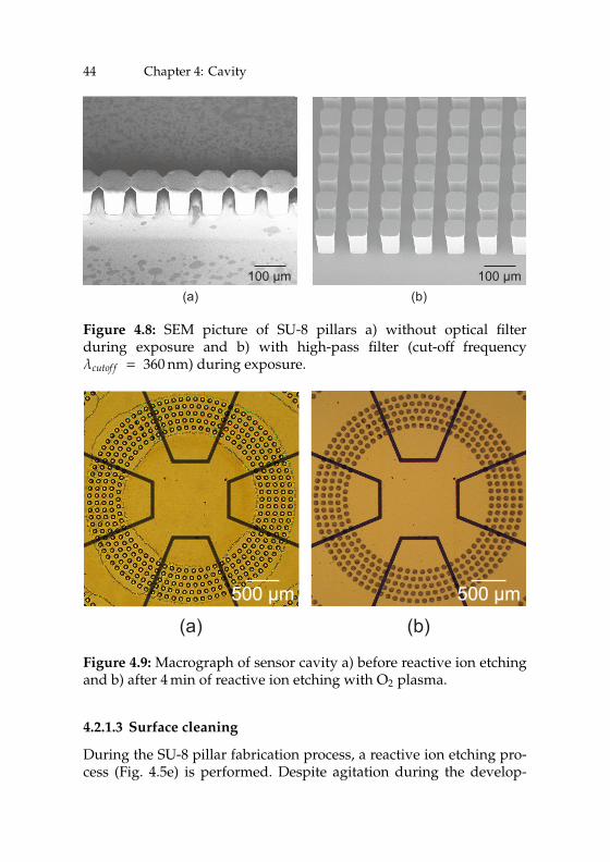
44 Chapter 4: Cavity
100 µm(a)
100 µm(b)
Figure 4.8: SEM picture of SU-8 pillars a) without optical filterduring exposure and b) with high-pass filter (cut-off frequencyλcutof f = 360 nm) during exposure.
(a)
500 µm
(b)
500 µm
Figure 4.9: Macrograph of sensor cavity a) before reactive ion etchingand b) after 4 min of reactive ion etching with O2 plasma.
4.2.1.3 Surface cleaning
During the SU-8 pillar fabrication process, a reactive ion etching pro-cess (Fig. 4.5e) is performed. Despite agitation during the develop-
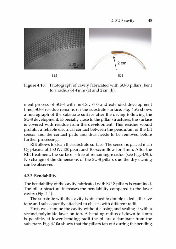
4.2. SU-8 cavity 45
2 cm
(a) (b)
5 cm 200 µm
Figure 4.10: Photograph of cavity fabricated with SU-8 pillars, bentto a radius of 4 mm (a) and 2 cm (b).
ment process of SU-8 with mr-Dev 600 and extended developmenttime, SU-8 residue remains on the substrate surface. Fig. 4.9a showsa micrograph of the substrate surface after the drying following theSU-8 development. Especially close to the pillar structures, the surfaceis covered with residue from the development. This residue wouldprohibit a reliable electrical contact between the pendulum of the tiltsensor and the contact pads and thus needs to be removed beforefurther processing.
RIE allows to clean the substrate surface. The sensor is placed in anO2 plasma at 150 W, 130µbar, and 100 sccm flow for 4 min. After theRIE treatment, the surface is free of remaining residue (see Fig. 4.9b).No change of the dimensions of the SU-8 pillars due the dry etchingcan be observed.
4.2.2 Bendability
The bendability of the cavity fabricated with SU-8 pillars is examined.The pillar structure increases the bendability compared to the layercavity (Fig. 4.4).
The substrate with the cavity is attached to double-sided adhesivetape and subsequently attached to objects with different radii.
First, we examine the cavity without closing and sealing it with asecond polyimide layer on top. A bending radius of down to 4 mmis possible, at lower bending radii the pillars delaminate from thesubstrate. Fig. 4.10a shows that the pillars fan out during the bending
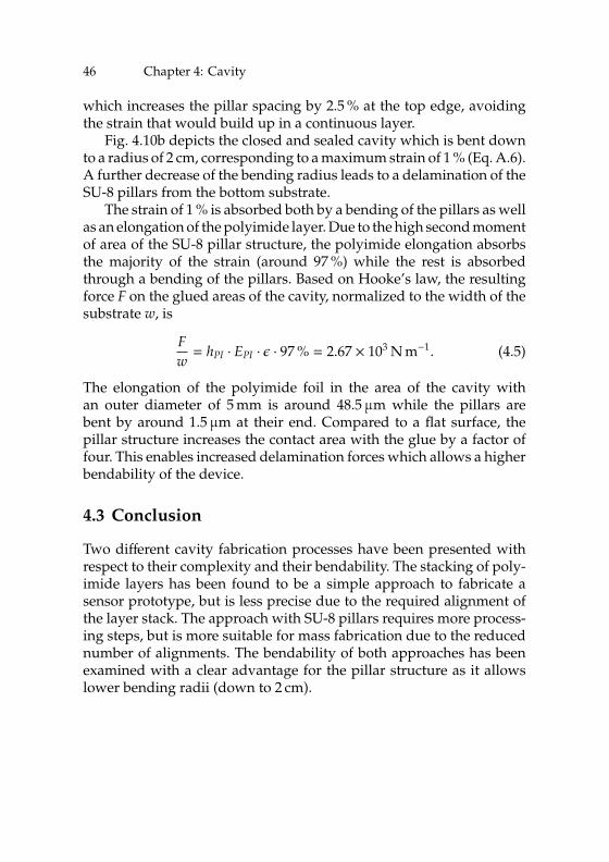
46 Chapter 4: Cavity
which increases the pillar spacing by 2.5 % at the top edge, avoidingthe strain that would build up in a continuous layer.
Fig. 4.10b depicts the closed and sealed cavity which is bent downto a radius of 2 cm, corresponding to a maximum strain of 1 % (Eq. A.6).A further decrease of the bending radius leads to a delamination of theSU-8 pillars from the bottom substrate.
The strain of 1 % is absorbed both by a bending of the pillars as wellas an elongation of the polyimide layer. Due to the high second momentof area of the SU-8 pillar structure, the polyimide elongation absorbsthe majority of the strain (around 97 %) while the rest is absorbedthrough a bending of the pillars. Based on Hooke’s law, the resultingforce F on the glued areas of the cavity, normalized to the width of thesubstrate w, is
F
w= hPI · EPI · ǫ · 97 % = 2.67 × 10³ N m−1. (4.5)
The elongation of the polyimide foil in the area of the cavity withan outer diameter of 5 mm is around 48.5µm while the pillars arebent by around 1.5µm at their end. Compared to a flat surface, thepillar structure increases the contact area with the glue by a factor offour. This enables increased delamination forces which allows a higherbendability of the device.
4.3 Conclusion
Two different cavity fabrication processes have been presented withrespect to their complexity and their bendability. The stacking of poly-imide layers has been found to be a simple approach to fabricate asensor prototype, but is less precise due to the required alignment ofthe layer stack. The approach with SU-8 pillars requires more process-ing steps, but is more suitable for mass fabrication due to the reducednumber of alignments. The bendability of both approaches has beenexamined with a clear advantage for the pillar structure as it allowslower bending radii (down to 2 cm).

5Contact mechanics
We discuss the interaction of the microsphere with the substrate surface andSU-8 cavity wall. The theory of the electrical contact between microsphere andsubstrate surface is presented and the resulting contact resistance is evaluated.The contact mechanics of the contact of microsphere and substrate surface andcavity wall are introduced and assessed with atomic force microscopy. Finally,lateral force microscopy determines the friction coefficient of the microsphereupon interaction with the different cavity materials.
48 Chapter 5: Contact mechanics
5.1 Electrical contact resistance
The electrical connection created by the microspheres with the sub-strate surface is a key factor for the successful operation of the tiltsensor. In the following, we focus on this topic in more detail to de-termine the parameters for creation of a reliable electrical contact withthe microspheres.
As described in chapter 3, the microspheres are solder spheres witha diameter of 250µm. In the following, the electrical contact resistanceof the microsphere with the substrate surface will be investigated.Therefore, we attach two gold coated substrates perpendicular to eachother, forming a V-shaped trench (see Fig. 5.2). The two gold layersdo not have an electrical connection. We place a single microsphereinside this trench and measure the electrical resistance between thetwo substrates.
With an uncoated microsphere, no electrical connection can be es-tablished at any tilt angle. Only once the load on the microsphere isincreased by additional weight, the oxide on the microsphere surfacecracks open and an electrical connection through the microsphere ismade. However, the required load is around 1 mN for tin-oxide [97]which exceeds the weight of a single microsphere (FG = 0.6µN) byseveral orders of magnitude. Therefore, a coating of the microspherewith gold (see chapter 3) is required for the formation of a reliableelectrical contact.
The electrical resistance of the setup is composed of several serialcomponents according to Fig. 5.1a: each contact point of the micro-sphere with the substrate exhibits the constriction resistance RC andthe Sharvin resistance RS [98]. In addition, the coating of the micro-sphere exhibits a resistance Rsp. All values are dependent on the radiusa of the a-spots which are the electrical contact areas. Solid surfacesare rough on a micro scale, thus the electrical contact is not formed onthe whole area of mechanical contact, but only on the contact of thea-spots.
• Constriction resistance RC
The constriction resistance is the classical ohmic resistance wherethe electrical flow in the contact is assumed continuous and canbe calculated according to [98]:
RC =ρ
2a. (5.1)
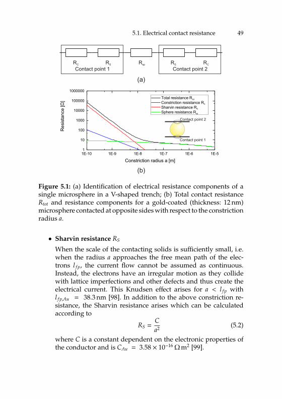
5.1. Electrical contact resistance 49
1E-10 1E-9 1E-8 1E-7 1E-6 1E-51
10
100
1000
10000
100000
1000000
Res
ista
nce
[Ω]
Constriction radius a [m]
Total resistance Rtot
Constriction resistance RC
Sharvin resistance RS
Sphere resistance Rsp
RC RS Rsp RS RC
(a)
(b)
Contact point 1 Contact point 2
Contact point 2
Contact point 1
Figure 5.1: (a) Identification of electrical resistance components of asingle microsphere in a V-shaped trench; (b) Total contact resistanceRtot and resistance components for a gold-coated (thickness: 12 nm)microsphere contacted at opposite sides with respect to the constrictionradius a.
• Sharvin resistance RS
When the scale of the contacting solids is sufficiently small, i.e.when the radius a approaches the free mean path of the elec-trons l f p, the current flow cannot be assumed as continuous.Instead, the electrons have an irregular motion as they collidewith lattice imperfections and other defects and thus create theelectrical current. This Knudsen effect arises for a < l f p withl f p,Au = 38.3 nm [98]. In addition to the above constriction re-sistance, the Sharvin resistance arises which can be calculatedaccording to
RS =C
a2(5.2)
where C is a constant dependent on the electronic properties ofthe conductor and is CAu = 3.58 × 10⁻¹⁶Ωm2 [99].
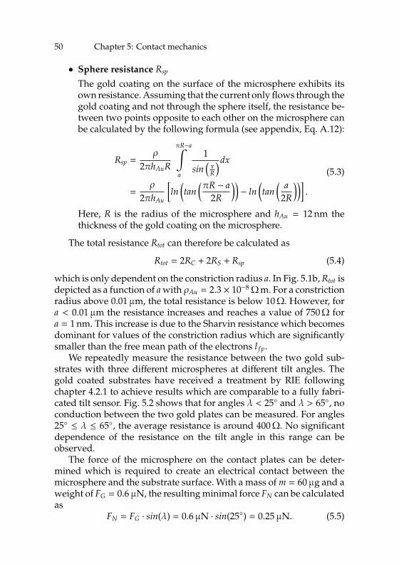
50 Chapter 5: Contact mechanics
• Sphere resistance Rsp
The gold coating on the surface of the microsphere exhibits itsown resistance. Assuming that the current only flows through thegold coating and not through the sphere itself, the resistance be-tween two points opposite to each other on the microsphere canbe calculated by the following formula (see appendix, Eq. A.12):
Rsp =ρ
2πhAuR
πR−a∫
a
1
sin(
xR
)dx
=ρ
2πhAu
[
ln(
tan(
πR − a
2R
))
− ln(
tan(
a
2R
))]
.
(5.3)
Here, R is the radius of the microsphere and hAu = 12 nm thethickness of the gold coating on the microsphere.
The total resistance Rtot can therefore be calculated as
Rtot = 2RC + 2RS + Rsp (5.4)
which is only dependent on the constriction radius a. In Fig. 5.1b, Rtot isdepicted as a function of a with ρAu = 2.3 × 10⁻⁸Ωm. For a constrictionradius above 0.01µm, the total resistance is below 10Ω. However, fora < 0.01µm the resistance increases and reaches a value of 750Ω fora = 1 nm. This increase is due to the Sharvin resistance which becomesdominant for values of the constriction radius which are significantlysmaller than the free mean path of the electrons l f p.
We repeatedly measure the resistance between the two gold sub-strates with three different microspheres at different tilt angles. Thegold coated substrates have received a treatment by RIE followingchapter 4.2.1 to achieve results which are comparable to a fully fabri-cated tilt sensor. Fig. 5.2 shows that for angles λ < 25 and λ > 65, noconduction between the two gold plates can be measured. For angles25 ≤ λ ≤ 65, the average resistance is around 400Ω. No significantdependence of the resistance on the tilt angle in this range can beobserved.
The force of the microsphere on the contact plates can be deter-mined which is required to create an electrical contact between themicrosphere and the substrate surface. With a mass of m = 60µg and aweight of FG = 0.6µN, the resulting minimal force FN can be calculatedas
FN = FG · sin(λ) = 0.6µN · sin(25) = 0.25µN. (5.5)
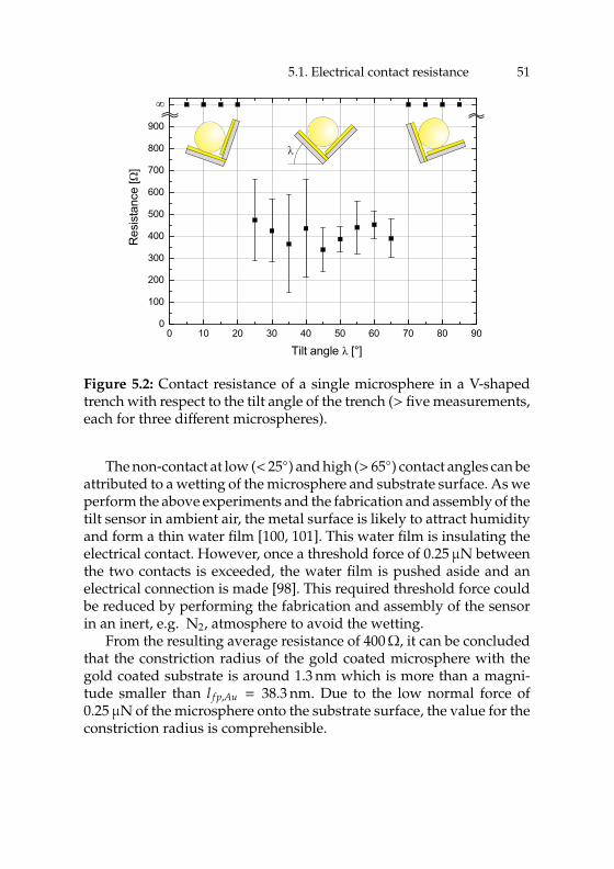
5.1. Electrical contact resistance 51
0 10 20 30 40 50 60 70 80 900
100
200
300
400
500
600
700
800
900R
esis
tanc
e [Ω
]
Tilt angle λ [°]
¥
λ
Figure 5.2: Contact resistance of a single microsphere in a V-shapedtrench with respect to the tilt angle of the trench (> five measurements,each for three different microspheres).
The non-contact at low (< 25) and high (> 65) contact angles can beattributed to a wetting of the microsphere and substrate surface. As weperform the above experiments and the fabrication and assembly of thetilt sensor in ambient air, the metal surface is likely to attract humidityand form a thin water film [100, 101]. This water film is insulating theelectrical contact. However, once a threshold force of 0.25µN betweenthe two contacts is exceeded, the water film is pushed aside and anelectrical connection is made [98]. This required threshold force couldbe reduced by performing the fabrication and assembly of the sensorin an inert, e.g. N2, atmosphere to avoid the wetting.
From the resulting average resistance of 400Ω, it can be concludedthat the constriction radius of the gold coated microsphere with thegold coated substrate is around 1.3 nm which is more than a magni-tude smaller than l f p,Au = 38.3 nm. Due to the low normal force of0.25µN of the microsphere onto the substrate surface, the value for theconstriction radius is comprehensible.
52 Chapter 5: Contact mechanics
5.2 Surface properties
We investigate the contact mechanics of the microsphere with the dif-ferent surfaces of the tilt sensor and relate the surface roughness to theexpected influence of adhesion forces and on the friction.
5.2.1 Surface roughness
In the following, the surface roughness of the different surfaces in-volved in the tilt sensor is measured by atomic force microscopy (AFM)which will be used to determine the influence of the roughness on theadhesion forces.
As the Young’s Modulus E of the polyimide EPI = 5.5 GPa is amagnitude smaller than the Young’s Modulus of the solder alloy withEsphere = 51 GPa, we can apply a theoretical model of a rigid sphereindenting an elastic surface. The theory of this model has been devel-oped by Heinrich Hertz (Hertzian Contact Theory) in 1881 [102] andallows to calculate the mechanical contact area of the microsphere withthe substrate surface. The force Find required to create an indentationof dind into the elastic surface can be calculated according to [103]
Find =43
E∗R1/2d3/2 (5.6)
where R is the radius of the sphere and E∗ is the Young’s modulusincorporating the poisson ratio ν for polyimide νPI = 0.32:
E∗ =EPI
(
1 − ν2PI
) = 6.13 GPa. (5.7)
From Eq. 5.5, the maximum normal force that one microsphere cre-ates, when an electrical connection is established, is FN,max = Find,max =
0.54µN at λ = 65. The maximum indentation dind thus is calculatedwith Eq. 5.6 according to
dind,max =
(34· 1
E∗· 1
R1/2· Find,max
)2/3
= 3.27 × 10⁻¹⁰ m. (5.8)
The mechanical contact radius amech is determined to [103]
amech =√
R · dind = 0.2µm. (5.9)
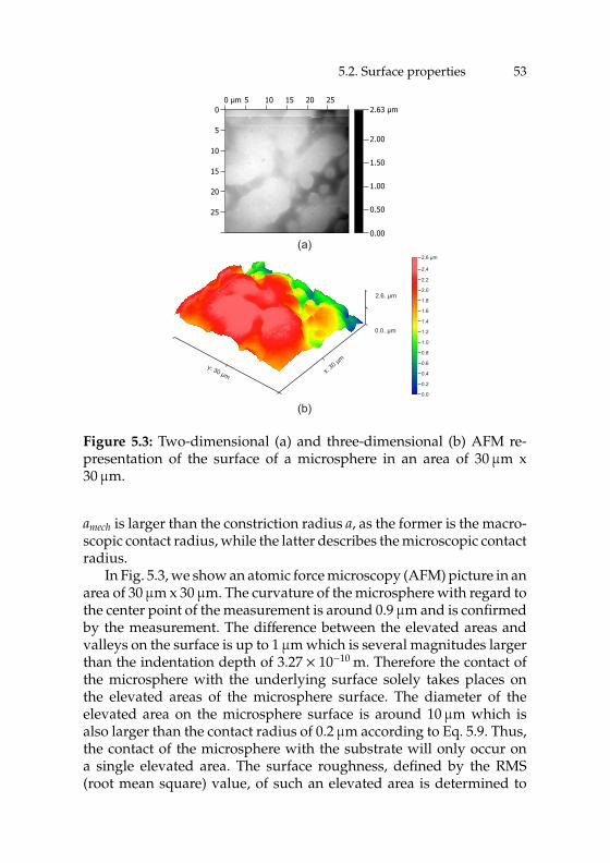
5.2. Surface properties 53
0 µm 5 10 15 20 250
5
10
15
20
25
2.63 µm
0.00
0.50
1.00
1.50
2.00
2.6 µm
2.4
2.2
2.0
1.8
1.6
1.4
1.2
1.0
0.8
0.6
0.4
0.2
0.0
y: 30 µm x: 30 µm
0.0. µm
2.6. µm
(a)
(b)
Figure 5.3: Two-dimensional (a) and three-dimensional (b) AFM re-presentation of the surface of a microsphere in an area of 30µm x30µm.
amech is larger than the constriction radius a, as the former is the macro-scopic contact radius, while the latter describes the microscopic contactradius.
In Fig. 5.3, we show an atomic force microscopy (AFM) picture in anarea of 30µm x 30µm. The curvature of the microsphere with regard tothe center point of the measurement is around 0.9µm and is confirmedby the measurement. The difference between the elevated areas andvalleys on the surface is up to 1µm which is several magnitudes largerthan the indentation depth of 3.27 × 10⁻¹⁰ m. Therefore the contact ofthe microsphere with the underlying surface solely takes places onthe elevated areas of the microsphere surface. The diameter of theelevated area on the microsphere surface is around 10µm which isalso larger than the contact radius of 0.2µm according to Eq. 5.9. Thus,the contact of the microsphere with the substrate will only occur ona single elevated area. The surface roughness, defined by the RMS(root mean square) value, of such an elevated area is determined to
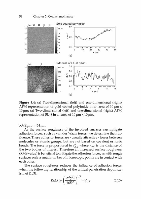
54 Chapter 5: Contact mechanics
0 µm 10 20 30 40
0
10
20
30
40
86 nm
0
20
30
40
50
60
70
0 10 20 30 40 50x [µm]
0.5
0.6
0.7
y [µ
m]
(a)
Gold coated polyimide
0 µm 5
0
5
602 nm
0
200
300
400
500
0 2 4 6 8 10x [µm]
0.1
0.2
0.3
0.4
0.5y
[µm
]
(b)
Side wall of SU-8 pillar
Figure 5.4: (a) Two-dimensional (left) and one-dimensional (right)AFM representation of gold coated polyimide in an area of 10µm x10µm; (a) Two-dimensional (left) and one-dimensional (right) AFMrepresentation of SU-8 in an area of 10µm x 10µm.
RMSsphere = 64 nm.As the surface roughness of the involved surfaces can mitigate
adhesion forces, such as van der Waals forces, we determine their in-fluence. These adhesion forces are - usually attractive - forces betweenmolecules or atomic groups, but are not based on covalent or ionicbonds. The force is proportional to r6
distwhere rdist is the distance of
the two bodies of interest. Therefore an increased surface roughness(RMS value) is beneficial to mitigate the adhesion forces, as with roughsurfaces only a small number of microscopic points are in contact witheach other.
The surface roughness reduces the influence of adhesion forceswhen the following relationship of the critical penetration depth dcrit
is met [103]:
RMS≫(
3π2γ2R
16E∗2
)1/3
= dcrit (5.10)
5.2. Surface properties 55
where γAu = 1.04 J m−2 is the surface energy of gold [104]. The rightside of Eq. 5.10 is computed to a value of dcrit = 18.8 nm.
The AFM scans on a gold coated polyimide surface as well as onthe side of a SU-8 pillar are shown in Fig. 5.4a and b, respectively. Theleft graph shows a representation of the surface over an area whilethe right graph shows the height characteristics for a single scan line.The gold surface shows a roughness with a value of RMSAu = 18.9 nm.On the contrary, the SU-8 shows a structure with grains of the size ofaround 200 nm which contribute to a roughness of RMSSU−8 = 82.9 nm.The values are summarized in Tab. 5.1.
Table 5.1: Root mean square (RMS) values for the surface roughnessof different surfaces.
Surface RMS value [nm]
Microsphere 64.0
Gold coated polyimide 18.9
SU-8 pillar side wall 82.9
The relation between the value of RMSsphere compared to RMSAu isin line with the observation on the contact resistance in chapter 5.1. Asmall constriction radius a is observed which is due to the high surfaceroughness of the microsphere.
Both the values of RMSsphere and RMSSU−8 are larger than the criticalpenetration depth dcrit = 18.8 nm. Therefore, in the case of a contact ofthe microsphere with the SU-8 pillars, the adhesion forces are mitigatedby the surface roughness of both materials and do not influence thefree movement of the microspheres inside the cavity.
The values of RMSAu and dcrit are in a similar range, the roughnessof the gold is not high enough to mitigate the adhesion forces. The ad-hesion forces of the gold coated polyimide will thus have an influenceon the movement of the microspheres. However, with the knowledgefrom chapter 5.1, it is not advisable to increase the surface roughnessby corresponding processing, as an increased roughness further de-creases the constriction radius a which in return increases the contactresistance further.
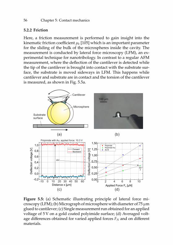
56 Chapter 5: Contact mechanics
5.2.2 Friction
Here, a friction measurement is performed to gain insight into thekinematic friction coefficient µk [105] which is an important parameterfor the sliding of the bulk of the microspheres inside the cavity. Themeasurement is conducted by lateral force microscopy (LFM), an ex-perimental technique for nanotribology. In contrast to a regular AFMmeasurement, where the deflection of the cantilever is detected whilethe tip of the cantilever is brought into contact with the substrate sur-face, the substrate is moved sideways in LFM. This happens whilecantilever and substrate are in contact and the torsion of the cantileveris measured, as shown in Fig. 5.5a.
(a) (b)
100 µm
(c)
-0,2
0,0
0,2
0,4
0,6
0,8
1,0 Forward Backward
Defl
ectio
n vo
ltage
[V]
Distance x [µm]
ΔV
Polyimide with Au, applied force: 10.3 V
-10 0 10 20 30 40 50 60
Cantilever
Microsphere
Substratesurface
(d)
0,00
0,25
0,50
0,75
1,00
1,25
1,50 Polyimide Polyimide+Au SU−8
Del
fect
ion
volta
ge [V
]
Applied Force F [µN]N
ΔV2
0 2 4 6 8 10
Figure 5.5: (a) Schematic illustrating principle of lateral force mi-croscopy (LFM); (b) Micrograph of microsphere with diameter of 75µmglued to cantilever; (c) Single measurement run obtained for an appliedvoltage of 5 V on a gold coated polyimide surface; (d) Averaged volt-age differences obtained for varied applied forces FN and on differentmaterials.
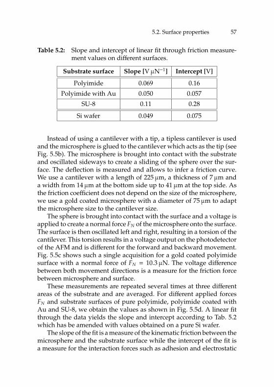
5.2. Surface properties 57
Table 5.2: Slope and intercept of linear fit through friction measure-ment values on different surfaces.
Substrate surface Slope [VµN−1] Intercept [V]
Polyimide 0.069 0.16
Polyimide with Au 0.050 0.057
SU-8 0.11 0.28
Si wafer 0.049 0.075
Instead of using a cantilever with a tip, a tipless cantilever is usedand the microsphere is glued to the cantilever which acts as the tip (seeFig. 5.5b). The microsphere is brought into contact with the substrateand oscillated sideways to create a sliding of the sphere over the sur-face. The deflection is measured and allows to infer a friction curve.We use a cantilever with a length of 225µm, a thickness of 7µm anda width from 14µm at the bottom side up to 41µm at the top side. Asthe friction coefficient does not depend on the size of the microsphere,we use a gold coated microsphere with a diameter of 75µm to adaptthe microsphere size to the cantilever size.
The sphere is brought into contact with the surface and a voltage isapplied to create a normal force FN of the microsphere onto the surface.The surface is then oscillated left and right, resulting in a torsion of thecantilever. This torsion results in a voltage output on the photodetectorof the AFM and is different for the forward and backward movement.Fig. 5.5c shows such a single acquisition for a gold coated polyimidesurface with a normal force of FN = 10.3µN. The voltage differencebetween both movement directions is a measure for the friction forcebetween microsphere and surface.
These measurements are repeated several times at three differentareas of the substrate and are averaged. For different applied forcesFN and substrate surfaces of pure polyimide, polyimide coated withAu and SU-8, we obtain the values as shown in Fig. 5.5d. A linear fitthrough the data yields the slope and intercept according to Tab. 5.2which has be amended with values obtained on a pure Si wafer.
The slope of the fit is a measure of the kinematic friction between themicrosphere and the substrate surface while the intercept of the fit isa measure for the interaction forces such as adhesion and electrostatic
58 Chapter 5: Contact mechanics
forces. The friction of the microsphere with a polyimide surface isreduced by around 30 % when the surface is coated with gold. Theslope is then identical to the friction on a Si wafer which shows thatthe gold coating reduces the friction to a minimum. From the previoussection, we know that the adhesion forces are not completely mitigatedby the roughness of the gold surface. However, as the gold surface isconductive, electrostatic forces can be ruled out as a source for theinteraction forces.
The interaction with a SU-8 surface shows a two-fold higher frictionthan with the gold surface. This is in line with the observations fromthe surface roughness in chapter 5.2.1 as the SU-8 surface has a higherroughness than the gold coated polyimide. The intercept is increasedby a factor of 5, indicating that the interaction forces are increased.Due to the surface roughness of SU-8, adhesion forces are negligible.However, electrostatic charges that build up in the SU-8, e.g. during thefabrication process, are not mitigated by the roughness and thereforelead to the observed high value for the interaction forces.
We conclude that the SU-8 surface exhibits a high friction coeffi-cient which inhibits a sliding movement of the microspheres in thecavity while the gold coated polyimide surface has a friction which issignificantly lower than the friction on SU-8 and similar to a smoothsilicon wafer surface.
5.3 Conclusion
We showed that a threshold pressure of the microspheres is requiredto penetrate the humidity film and create an electrical contact. Theresistance of the electrical contact is around 400Ω which is due tomicroscale effects of the electron movement in the contact area. Theroughness of the interacting surfaces was measured and examinedwhich showed that the adhesion forces between SU-8 and the micro-sphere can be neglected while the adhesion forces of the gold coatedpolyimide will have an influence on the microsphere. The examinationof the kinematic friction of the microsphere on surfaces of gold coatedpolyimide and pure SU-8 confirms the conclusions that due to the in-creased surface roughness the friction on SU-8 is dominant comparedto a gold surface.
6Sensor modeling
The tilt sensor principle entails several geometrical design parameters thathave an influence on the sensor characteristics. We introduce the differentdesign parameters and define the evaluation criteria. A comprehensive modelis introduced to quantify the leverage of the design parameters on the charac-teristics of the tilt sensor.
60 Chapter 6: Sensor modeling
6.1 Definition of parameters
In the following, we introduce and define the design parameters of thetilt sensor and present the evaluation parameters which are used todetermine the influence of the design parameters.
6.1.1 Design parameters
The sensor design in Fig. 2.3 entails several geometrical design pa-rameters that can have an influence on the sensor characteristics. Weinvestigate parameters that describe the design and layout of the con-tact pads on the sensor substrate (Fig. 6.1) as well as specificationsconcerning the cavity and pendulum (Fig. 6.2):
• Number of contact pads N: The number of contact pads inside thecavity (Fig. 6.1a).
• Sensor pad design: Different designs are possible for the design ofthe sensor contact pads inside the cavity. Here, we evaluate threedifferent arrangements (Fig. 6.1b):
– Trapezoidal: Trapezoidal contact pads alternating with aground plane.
– No ground: Trapezoidal contact pads with no ground planebetween the pads.
– Rectangular: Rectangular contact pads alternating with aground plane.
• Inner contact radius rcontact: The inner radius of the contact pads, i.e.the distance of the contact pads from the sensor center (Fig. 6.1c).
• Ratio of ground to contact pad ηpad: The ratio of the angle of thecontact pad αpad in relation to the angular resolution αres as will bedefined in Eq. 6.2 (Fig. 6.1d), applicable for pad styles Trapezoidal
and Rectangular where 0 ≤ ηpad =αpad
αres≤ 2.
• Radius of sensor cavity rcavity: The inner radius of the sensor cavitydefining the movement area of the pendulum (Fig. 6.2a).
• Amount of microspheres Nspheres: The amount of microspheres in-side the cavity, determining how many contact pads are con-nected at a given point in time. We represent the contact area
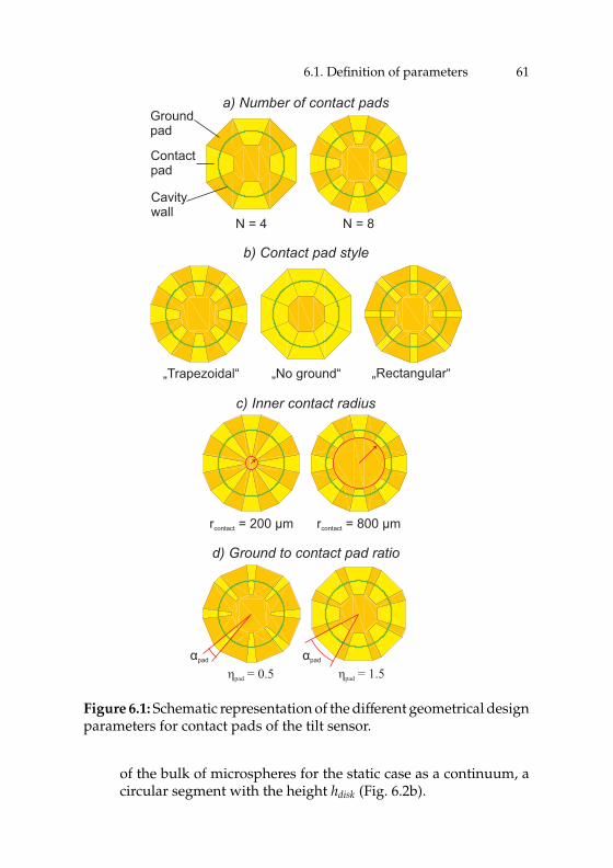
6.1. Definition of parameters 61
„No ground“ „Rectangular“
b) Contact pad style
„Trapezoidal“
r = 200 µmcontact r = 800 µmcontact
c) Inner contact radius
N = 4 N = 8
a) Number of contact padsGroundpad
Contactpad
Cavitywall
η = 0.5pad η = 1.5pad
d) Ground to contact pad ratio
αpad αpad
Figure 6.1: Schematic representation of the different geometrical designparameters for contact pads of the tilt sensor.
of the bulk of microspheres for the static case as a continuum, acircular segment with the height hdisk (Fig. 6.2b).
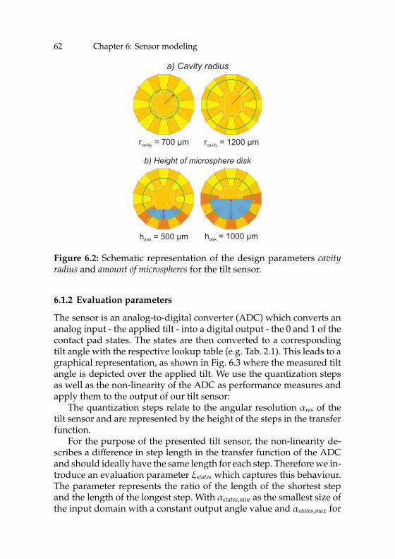
62 Chapter 6: Sensor modeling
b) Height of microsphere disk
h = 1000 µmdiskh = 500 µmdisk
r = 700 µmcavity r = 1200 µmcavity
a) Cavity radius
Figure 6.2: Schematic representation of the design parameters cavityradius and amount of microspheres for the tilt sensor.
6.1.2 Evaluation parameters
The sensor is an analog-to-digital converter (ADC) which converts ananalog input - the applied tilt - into a digital output - the 0 and 1 of thecontact pad states. The states are then converted to a correspondingtilt angle with the respective lookup table (e.g. Tab. 2.1). This leads to agraphical representation, as shown in Fig. 6.3 where the measured tiltangle is depicted over the applied tilt. We use the quantization stepsas well as the non-linearity of the ADC as performance measures andapply them to the output of our tilt sensor:
The quantization steps relate to the angular resolution αres of thetilt sensor and are represented by the height of the steps in the transferfunction.
For the purpose of the presented tilt sensor, the non-linearity de-scribes a difference in step length in the transfer function of the ADCand should ideally have the same length for each step. Therefore we in-troduce an evaluation parameter ξstates which captures this behaviour.The parameter represents the ratio of the length of the shortest stepand the length of the longest step. With αstates,min as the smallest size ofthe input domain with a constant output angle value and αstates,max for
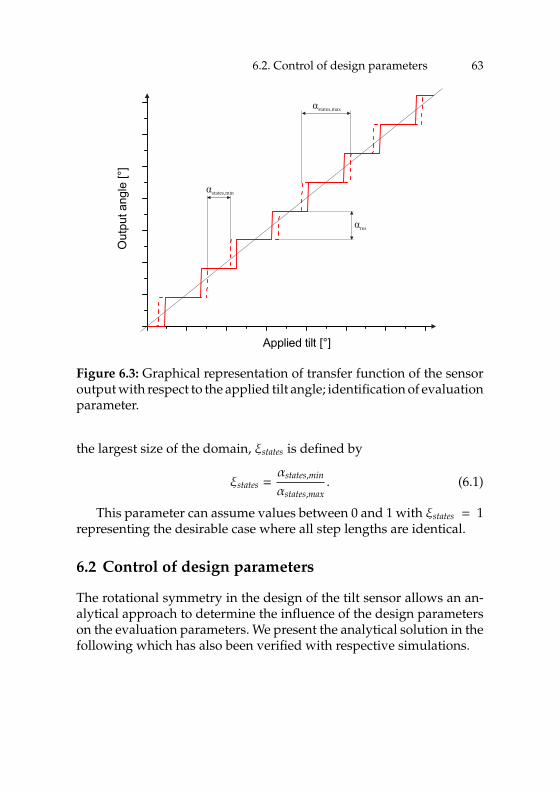
6.2. Control of design parameters 63
Out
put a
ngle
[°]
Applied tilt [°]
αstates,min
αstates,max
αres
Figure 6.3: Graphical representation of transfer function of the sensoroutput with respect to the applied tilt angle; identification of evaluationparameter.
the largest size of the domain, ξstates is defined by
ξstates =αstates,min
αstates,max. (6.1)
This parameter can assume values between 0 and 1 with ξstates = 1representing the desirable case where all step lengths are identical.
6.2 Control of design parameters
The rotational symmetry in the design of the tilt sensor allows an an-alytical approach to determine the influence of the design parameterson the evaluation parameters. We present the analytical solution in thefollowing which has also been verified with respective simulations.
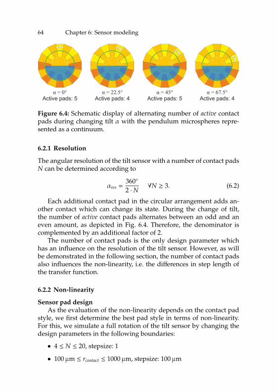
64 Chapter 6: Sensor modeling
α = 0°Active pads: 5
α = 22.5°Active pads: 4
α = 45°Active pads: 5
α = 67.5°Active pads: 4
Figure 6.4: Schematic display of alternating number of active contactpads during changing tilt α with the pendulum microspheres repre-sented as a continuum.
6.2.1 Resolution
The angular resolution of the tilt sensor with a number of contact padsN can be determined according to
αres =360
2 ·N ∀N ≥ 3. (6.2)
Each additional contact pad in the circular arrangement adds an-other contact which can change its state. During the change of tilt,the number of active contact pads alternates between an odd and aneven amount, as depicted in Fig. 6.4. Therefore, the denominator iscomplemented by an additional factor of 2.
The number of contact pads is the only design parameter whichhas an influence on the resolution of the tilt sensor. However, as willbe demonstrated in the following section, the number of contact padsalso influences the non-linearity, i.e. the differences in step length ofthe transfer function.
6.2.2 Non-linearity
Sensor pad designAs the evaluation of the non-linearity depends on the contact pad
style, we first determine the best pad style in terms of non-linearity.For this, we simulate a full rotation of the tilt sensor by changing thedesign parameters in the following boundaries:
• 4 ≤ N ≤ 20, stepsize: 1
• 100µm ≤ rcontact ≤ 1000µm, stepsize: 100µm
6.2. Control of design parameters 65
• 0.05 ≤ ηpad ≤ 1.95, stepsize: 0.05
• rcavity = 1000µm
• 250µm ≤ hdisk ≤ 1750µm, stepsize: 25µm
For each parameter combination, we determine the non-linearity ξstates
and subsequently calculate the average for all combinations. The re-sulting average value for each pad style is given in Tab. 6.1.
Table 6.1: Average value for evaluation parameter ξstates for each padstyle after a parameter sweep across all other design parameters.
Contact pad style Mean of ξstates
Trapezoidal 0.3818
No ground 0.3783
Rectangular 0.3673
The noted values are less than 0.4 as the values are obtained by av-eraging over all obtained ξstates for all parameter sets. The table showsa dependency of the non-linearity on the contact pad style. We see anadvantage for the pad style Trapezoidal, as the larger the value of ξstates
is, the smaller is the difference in step lengths in the transfer function.The style No ground with the missing ground plane between the contactpads relates to a pad style Trapezoidal where the contact to pad ratio isηpad = 2. The style Rectangular is similar to the style Trapezoidal, but asthe trapezoidal shape caters more for the circular design of the padsand due to the reduced contact area of the rectangular pads, the trape-zoidal pad design shows the best performance. Therefore all furtheranalysis will be focusing on the trapezoidal design.
Radius of sensor cavityThe cavity radius rcavity has no influence on the non-linearity of the
tilt sensor, it merely affects the size of the sensor. As stated in the spec-ifications in chapter 2.3, the diameter of the sensor should be in therange of several millimeter. However, the cavity radius should also benot too small to ensure a sufficient amount of microspheres in the cav-ity. The microsphere disk consists of discrete particles which shouldbe taken into account. We select rcavity = 1000µm which corresponds to
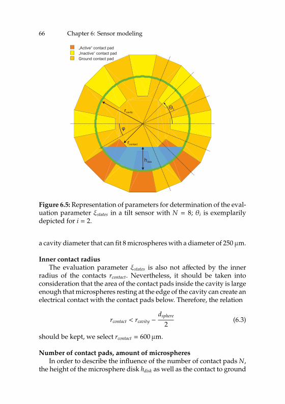
66 Chapter 6: Sensor modeling
Θ2
φ
rcavity
hdisk
rcontact
„Active“ contact pad„Inactive“ contact padGround contact pad
Figure 6.5: Representation of parameters for determination of the eval-uation parameter ξstates in a tilt sensor with N = 8; θi is exemplarilydepicted for i = 2.
a cavity diameter that can fit 8 microspheres with a diameter of 250µm.
Inner contact radiusThe evaluation parameter ξstates is also not affected by the inner
radius of the contacts rcontact. Nevertheless, it should be taken intoconsideration that the area of the contact pads inside the cavity is largeenough that microspheres resting at the edge of the cavity can create anelectrical contact with the contact pads below. Therefore, the relation
rcontact < rcavity −dsphere
2(6.3)
should be kept, we select rcontact = 600µm.
Number of contact pads, amount of microspheresIn order to describe the influence of the number of contact pads N,
the height of the microsphere disk hdisk as well as the contact to ground
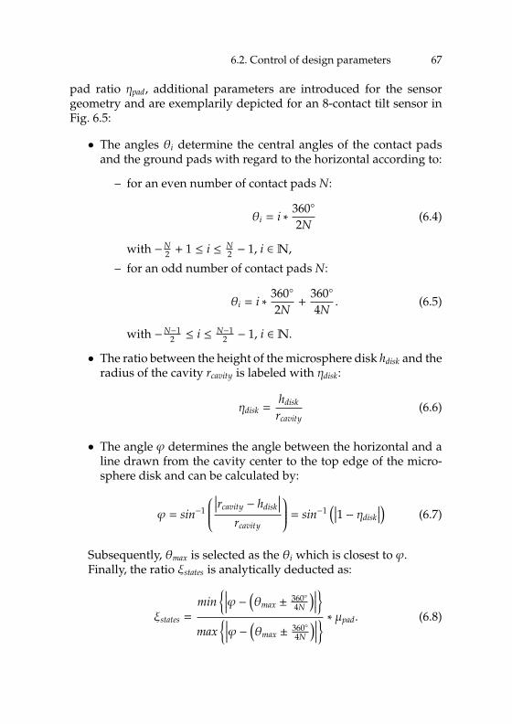
6.2. Control of design parameters 67
pad ratio ηpad, additional parameters are introduced for the sensorgeometry and are exemplarily depicted for an 8-contact tilt sensor inFig. 6.5:
• The angles θi determine the central angles of the contact padsand the ground pads with regard to the horizontal according to:
– for an even number of contact pads N:
θi = i ∗ 360
2N(6.4)
with −N2 + 1 ≤ i ≤ N
2 − 1, i ∈N,
– for an odd number of contact pads N:
θi = i ∗ 360
2N+
360
4N. (6.5)
with −N−12 ≤ i ≤ N−1
2 − 1, i ∈N.
• The ratio between the height of the microsphere disk hdisk and theradius of the cavity rcavity is labeled with ηdisk:
ηdisk =hdisk
rcavity(6.6)
• The angle ϕ determines the angle between the horizontal and aline drawn from the cavity center to the top edge of the micro-sphere disk and can be calculated by:
ϕ = sin−1
∣
∣
∣rcavity − hdisk
∣
∣
∣
rcavity
= sin−1(∣
∣
∣1 − ηdisk
∣
∣
∣
)
(6.7)
Subsequently, θmax is selected as the θi which is closest to ϕ.Finally, the ratio ξstates is analytically deducted as:
ξstates =
min∣
∣
∣
∣
ϕ −(
θmax ± 3604N
)
∣
∣
∣
∣
max∣
∣
∣
∣
ϕ −(
θmax ± 3604N
)
∣
∣
∣
∣
∗ µpad. (6.8)
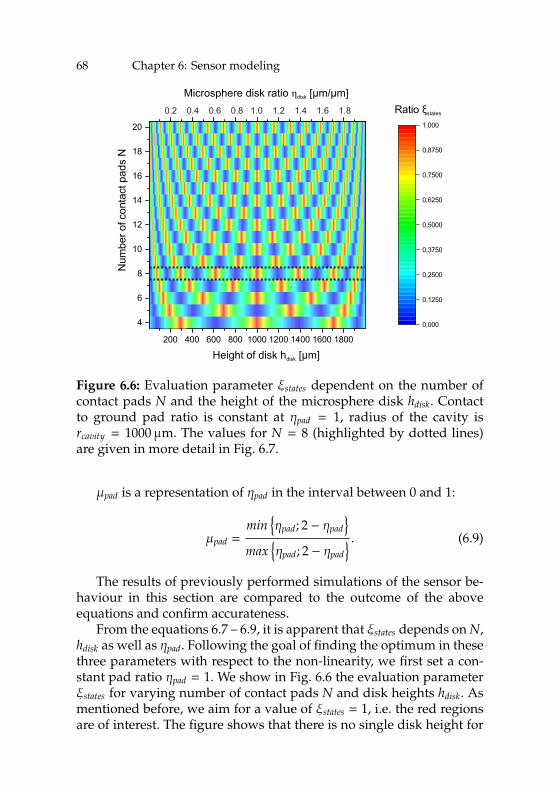
68 Chapter 6: Sensor modeling
200 400 600 800 1000 1200 1400 1600 1800
Height of disk h [µm]disk
0,000
0,1250
0,2500
0,3750
0,5000
0,6250
0,7500
0,8750
Ratio ξstates
1,000
4
6
8
10
12
14
16
18
20N
umbe
r of c
onta
ct p
ads
N0.2 0.4 0.6 0.8 1.0 1.2 1.4 1.6 1.8
Microsphere disk ratio η [µm/µm]disk
Figure 6.6: Evaluation parameter ξstates dependent on the number ofcontact pads N and the height of the microsphere disk hdisk. Contactto ground pad ratio is constant at ηpad = 1, radius of the cavity isrcavity = 1000µm. The values for N = 8 (highlighted by dotted lines)are given in more detail in Fig. 6.7.
µpad is a representation of ηpad in the interval between 0 and 1:
µpad =min
ηpad; 2 − ηpad
max
ηpad; 2 − ηpad
. (6.9)
The results of previously performed simulations of the sensor be-haviour in this section are compared to the outcome of the aboveequations and confirm accurateness.
From the equations 6.7 – 6.9, it is apparent that ξstates depends on N,hdisk as well as ηpad. Following the goal of finding the optimum in thesethree parameters with respect to the non-linearity, we first set a con-stant pad ratio ηpad = 1. We show in Fig. 6.6 the evaluation parameterξstates for varying number of contact pads N and disk heights hdisk. Asmentioned before, we aim for a value of ξstates = 1, i.e. the red regionsare of interest. The figure shows that there is no single disk height for
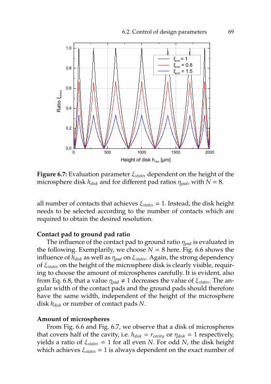
6.2. Control of design parameters 69
0 500 1000 1500 20000,0
0,2
0,4
0,6
0,8
1,0
Rat
io ξ
stat
es
Height of disk h [µm]disk
ξ = 1pad
ξ = 0.8pad
ξ = 1.5pad
Figure 6.7: Evaluation parameter ξstates dependent on the height of themicrosphere disk hdisk and for different pad ratios ηpad, with N = 8.
all number of contacts that achieves ξstates = 1. Instead, the disk heightneeds to be selected according to the number of contacts which arerequired to obtain the desired resolution.
Contact pad to ground pad ratioThe influence of the contact pad to ground ratio ηpad is evaluated in
the following. Exemplarily, we choose N = 8 here. Fig. 6.6 shows theinfluence of hdisk as well as ηpad on ξstates. Again, the strong dependencyof ξstates on the height of the microsphere disk is clearly visible, requir-ing to choose the amount of microspheres carefully. It is evident, alsofrom Eq. 6.8, that a value ηpad , 1 decreases the value of ξstates. The an-gular width of the contact pads and the ground pads should thereforehave the same width, independent of the height of the microspheredisk hdisk or number of contact pads N.
Amount of microspheresFrom Fig. 6.6 and Fig. 6.7, we observe that a disk of microspheres
that covers half of the cavity, i.e. hdisk = rcavity or ηdisk = 1 respectively,yields a ratio of ξstates = 1 for all even N. For odd N, the disk heightwhich achieves ξstates = 1 is always dependent on the exact number of
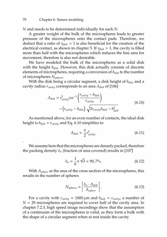
70 Chapter 6: Sensor modeling
N and needs to be determined individually for each N.A greater weight of the bulk of the microspheres leads to greater
pressure of the microspheres onto the contact pads. Therefore, wededuct that a ratio of ηdisk = 1 is also beneficial for the creation of theelectrical contact, as shown in chapter 5. If ηdisk > 1, the cavity is filledmore than half with the microspheres which reduces the free area formovement, therefore is also not desirable.
We have modeled the bulk of the microspheres as a solid diskwith the height hdisk. However, this disk actually consists of discreteelements of microspheres, requiring a conversion of hdisk to the numberof microspheres Nspheres.
With the disk being a circular segment, a disk height of hdisk and acavity radius rcavity corresponds to an area Adisk of [106]
Adisk = r2cavitycos−1
(
rcavity − hdisk
rcavity
)
−(
rcavity − hdisk
)
√
2rcavityhdisk − h2disk.
(6.10)
As mentioned above, for an even number of contacts, the ideal diskheight is hdisk = rcavity and Eq. 6.10 simplifies to
Adisk =π
2r2
cavity. (6.11)
.We assume here that the microspheres are densely packed, therefore
the packing density δn (fraction of area covered) results in [107]
δn =16π√
3 ≈ 90, 7%. (6.12)
With Asphere as the area of the cross section of the microspheres, thisresults in the number of spheres
Nspheres =
⌈
δn · Adisk
Asphere
⌉
. (6.13)
For a cavity with rcavity = 1000µm and hdisk = rcavity, a number ofN = 29 microspheres are required to cover half of the cavity area. Inchapter 7.2.3, high speed image recordings show that the assumptionof a continuum of the microspheres is valid, as they form a bulk withthe shape of a circular segment when at rest inside the cavity.

6.3. Conclusion 71
6.3 Conclusion
We have shown that the performance of the tilt sensor mainly dependson the number of contact pads N, the number of microspheres Nspheres
as well as the contact pad to ground pad ratio ηpad. For the followingsection 7 we select the parameter values as follows:
a) Number of contact pads:
• N = 4, achieving a resolution of αres = 45
• N = 8, achieving a resolution of αres = 22.5
b) Sensor pad design: Trapezoidal
c) Inner contact radius: rcontact = 600µm
d) Radius of sensor cavity: rcavity = 1000µm
e) Ratio of ground to contact pad: ηpad = 1
f) Amount of microspheres: hdisk = rcavity, resulting in Nspheres = 29.
We fabricated the corresponding tilt sensors and evaluate theircharacteristics in the following chapter.

7Evaluation
We perform an evaluation of the characteristics of both the tilt switch as wellas the tilt sensor. Both devices are first characterized under static conditions.We also observe the movements of the microspheres in the cavity of the tiltsensor before performing a dynamic evaluation of the tilt sensor.
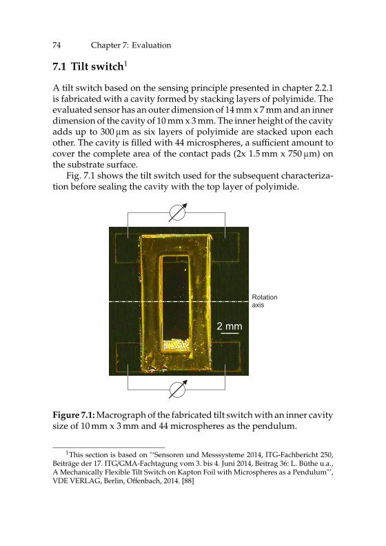
74 Chapter 7: Evaluation
7.1 Tilt switch1
A tilt switch based on the sensing principle presented in chapter 2.2.1is fabricated with a cavity formed by stacking layers of polyimide. Theevaluated sensor has an outer dimension of 14 mm x 7 mm and an innerdimension of the cavity of 10 mm x 3 mm. The inner height of the cavityadds up to 300µm as six layers of polyimide are stacked upon eachother. The cavity is filled with 44 microspheres, a sufficient amount tocover the complete area of the contact pads (2x 1.5 mm x 750µm) onthe substrate surface.
Fig. 7.1 shows the tilt switch used for the subsequent characteriza-tion before sealing the cavity with the top layer of polyimide.
2 mm
Rotationaxis
Figure 7.1: Macrograph of the fabricated tilt switch with an inner cavitysize of 10 mm x 3 mm and 44 microspheres as the pendulum.
1This section is based on "‘Sensoren und Messsysteme 2014, ITG-Fachbericht 250,Beiträge der 17. ITG/GMA-Fachtagung vom 3. bis 4. Juni 2014, Beitrag 36: L. Büthe u.a.,A Mechanically Flexible Tilt Switch on Kapton Foil with Microspheres as a Pendulum"’,VDE VERLAG, Berlin, Offenbach, 2014. [88]
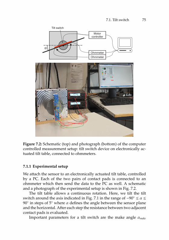
7.1. Tilt switch 75
Ohmmeter
Motorcontroller
Tilt switch
Ohmmeterα
Figure 7.2: Schematic (top) and photograph (bottom) of the computercontrolled measurement setup: tilt switch device on electronically ac-tuated tilt table, connected to ohmmeters.
7.1.1 Experimental setup
We attach the sensor to an electronically actuated tilt table, controlledby a PC. Each of the two pairs of contact pads is connected to anohmmeter which then send the data to the PC as well. A schematicand a photograph of the experimental setup is shown in Fig. 7.2.
The tilt table allows a continuous rotation. Here, we tilt the tiltswitch around the axis indicated in Fig. 7.1 in the range of −90 ≤ α ≤90 in steps of 5 where α defines the angle between the sensor planeand the horizontal. After each step the resistance between two adjacentcontact pads is evaluated.
Important parameters for a tilt switch are the make angle αmake
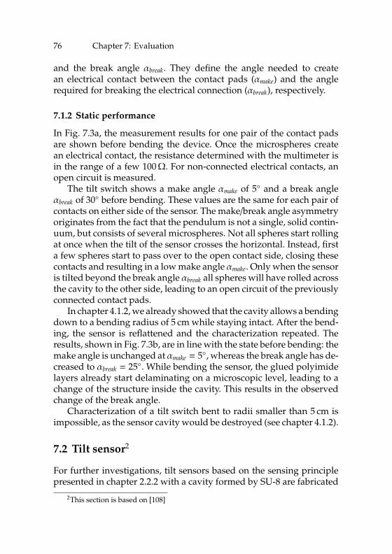
76 Chapter 7: Evaluation
and the break angle αbreak. They define the angle needed to createan electrical contact between the contact pads (αmake) and the anglerequired for breaking the electrical connection (αbreak), respectively.
7.1.2 Static performance
In Fig. 7.3a, the measurement results for one pair of the contact padsare shown before bending the device. Once the microspheres createan electrical contact, the resistance determined with the multimeter isin the range of a few 100Ω. For non-connected electrical contacts, anopen circuit is measured.
The tilt switch shows a make angle αmake of 5 and a break angleαbreak of 30 before bending. These values are the same for each pair ofcontacts on either side of the sensor. The make/break angle asymmetryoriginates from the fact that the pendulum is not a single, solid contin-uum, but consists of several microspheres. Not all spheres start rollingat once when the tilt of the sensor crosses the horizontal. Instead, firsta few spheres start to pass over to the open contact side, closing thesecontacts and resulting in a low make angle αmake. Only when the sensoris tilted beyond the break angle αbreak all spheres will have rolled acrossthe cavity to the other side, leading to an open circuit of the previouslyconnected contact pads.
In chapter 4.1.2, we already showed that the cavity allows a bendingdown to a bending radius of 5 cm while staying intact. After the bend-ing, the sensor is reflattened and the characterization repeated. Theresults, shown in Fig. 7.3b, are in line with the state before bending: themake angle is unchanged at αmake = 5, whereas the break angle has de-creased to αbreak = 25. While bending the sensor, the glued polyimidelayers already start delaminating on a microscopic level, leading to achange of the structure inside the cavity. This results in the observedchange of the break angle.
Characterization of a tilt switch bent to radii smaller than 5 cm isimpossible, as the sensor cavity would be destroyed (see chapter 4.1.2).
7.2 Tilt sensor2
For further investigations, tilt sensors based on the sensing principlepresented in chapter 2.2.2 with a cavity formed by SU-8 are fabricated
2This section is based on [108]
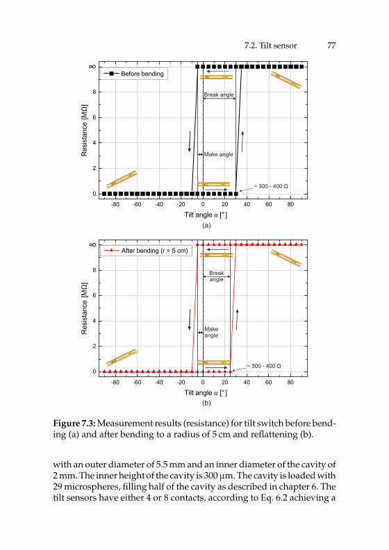
7.2. Tilt sensor 77
-80 -60 -40 -20 0 20 40 60 80
0
2
4
6
8
10 Before bending
Res
ista
nce
[MΩ
]
Tilt angle α [° ]
∞ 10
Make angle
Break angle
(a)
-80 -60 -40 -20 0 20 40 60 80
0
2
4
6
8
10 After bending (r = 5 cm)
Res
ista
nce
[MΩ
]
Tilt angle α [° ]
∞ 10
Makeangle
Breakangle
(b)
∞
∞
~ 300 - 400 Ω
~ 300 - 400 Ω
Figure 7.3: Measurement results (resistance) for tilt switch before bend-ing (a) and after bending to a radius of 5 cm and reflattening (b).
with an outer diameter of 5.5 mm and an inner diameter of the cavity of2 mm. The inner height of the cavity is 300µm. The cavity is loaded with29 microspheres, filling half of the cavity as described in chapter 6. Thetilt sensors have either 4 or 8 contacts, according to Eq. 6.2 achieving a
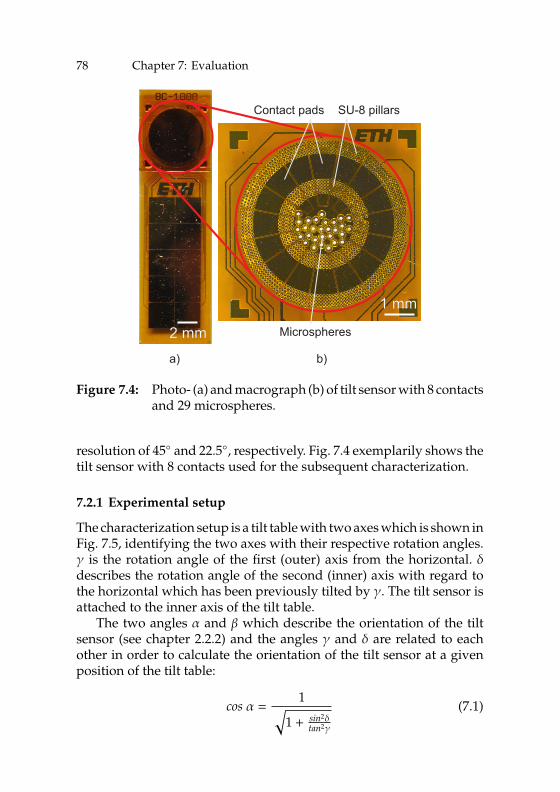
78 Chapter 7: Evaluation
1 mm
1 mm
2 mm
Contact pads SU-8 pillars
Microspheres
a) b)
Figure 7.4: Photo- (a) and macrograph (b) of tilt sensor with 8 contactsand 29 microspheres.
resolution of 45 and 22.5, respectively. Fig. 7.4 exemplarily shows thetilt sensor with 8 contacts used for the subsequent characterization.
7.2.1 Experimental setup
The characterization setup is a tilt table with two axes which is shown inFig. 7.5, identifying the two axes with their respective rotation angles.γ is the rotation angle of the first (outer) axis from the horizontal. δdescribes the rotation angle of the second (inner) axis with regard tothe horizontal which has been previously tilted by γ. The tilt sensor isattached to the inner axis of the tilt table.
The two angles α and β which describe the orientation of the tiltsensor (see chapter 2.2.2) and the angles γ and δ are related to eachother in order to calculate the orientation of the tilt sensor at a givenposition of the tilt table:
cos α =1
√
1 + sin2δtan2γ
(7.1)
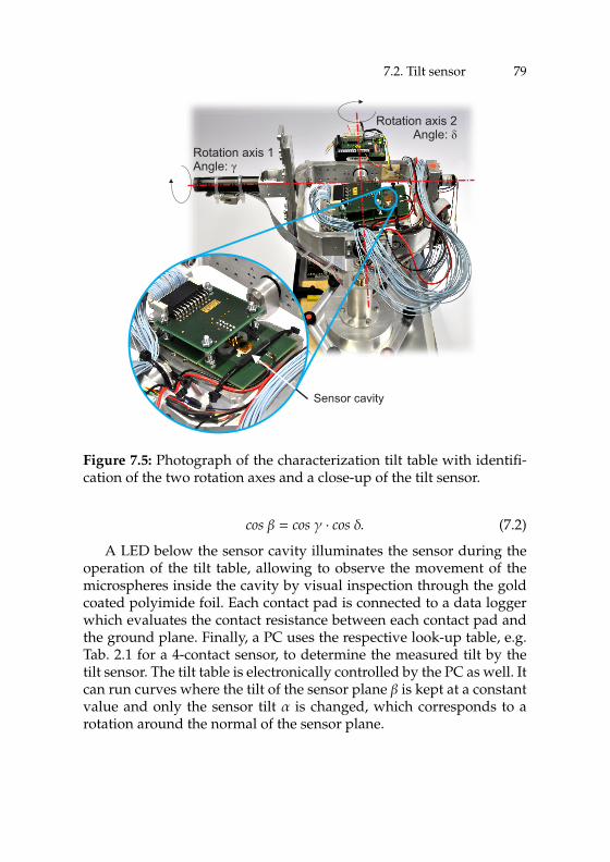
7.2. Tilt sensor 79
Rotation axis 1Angle: γ
Rotation axis 2Angle: δ
Sensor cavity
Figure 7.5: Photograph of the characterization tilt table with identifi-cation of the two rotation axes and a close-up of the tilt sensor.
cos β = cos γ · cos δ. (7.2)
A LED below the sensor cavity illuminates the sensor during theoperation of the tilt table, allowing to observe the movement of themicrospheres inside the cavity by visual inspection through the goldcoated polyimide foil. Each contact pad is connected to a data loggerwhich evaluates the contact resistance between each contact pad andthe ground plane. Finally, a PC uses the respective look-up table, e.g.Tab. 2.1 for a 4-contact sensor, to determine the measured tilt by thetilt sensor. The tilt table is electronically controlled by the PC as well. Itcan run curves where the tilt of the sensor plane β is kept at a constantvalue and only the sensor tilt α is changed, which corresponds to arotation around the normal of the sensor plane.
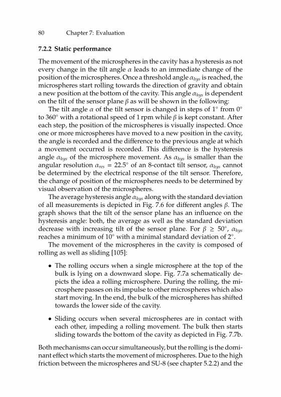
80 Chapter 7: Evaluation
7.2.2 Static performance
The movement of the microspheres in the cavity has a hysteresis as notevery change in the tilt angle α leads to an immediate change of theposition of the microspheres. Once a threshold angleαhys is reached, themicrospheres start rolling towards the direction of gravity and obtaina new position at the bottom of the cavity. This angle αhys is dependenton the tilt of the sensor plane β as will be shown in the following:
The tilt angle α of the tilt sensor is changed in steps of 1 from 0
to 360 with a rotational speed of 1 rpm while β is kept constant. Aftereach step, the position of the microspheres is visually inspected. Onceone or more microspheres have moved to a new position in the cavity,the angle is recorded and the difference to the previous angle at whicha movement occurred is recorded. This difference is the hysteresisangle αhys of the microsphere movement. As αhys is smaller than theangular resolution αres = 22.5 of an 8-contact tilt sensor, αhys cannotbe determined by the electrical response of the tilt sensor. Therefore,the change of position of the microspheres needs to be determined byvisual observation of the microspheres.
The average hysteresis angle αhys along with the standard deviationof all measurements is depicted in Fig. 7.6 for different angles β. Thegraph shows that the tilt of the sensor plane has an influence on thehysteresis angle: both, the average as well as the standard deviationdecrease with increasing tilt of the sensor plane. For β ≥ 50, αhys
reaches a minimum of 10 with a minimal standard deviation of 2.The movement of the microspheres in the cavity is composed of
rolling as well as sliding [105]:
• The rolling occurs when a single microsphere at the top of thebulk is lying on a downward slope. Fig. 7.7a schematically de-picts the idea a rolling microsphere. During the rolling, the mi-crosphere passes on its impulse to other microspheres which alsostart moving. In the end, the bulk of the microspheres has shiftedtowards the lower side of the cavity.
• Sliding occurs when several microspheres are in contact witheach other, impeding a rolling movement. The bulk then startssliding towards the bottom of the cavity as depicted in Fig. 7.7b.
Both mechanisms can occur simultaneously, but the rolling is the domi-nant effect which starts the movement of microspheres. Due to the highfriction between the microspheres and SU-8 (see chapter 5.2.2) and the
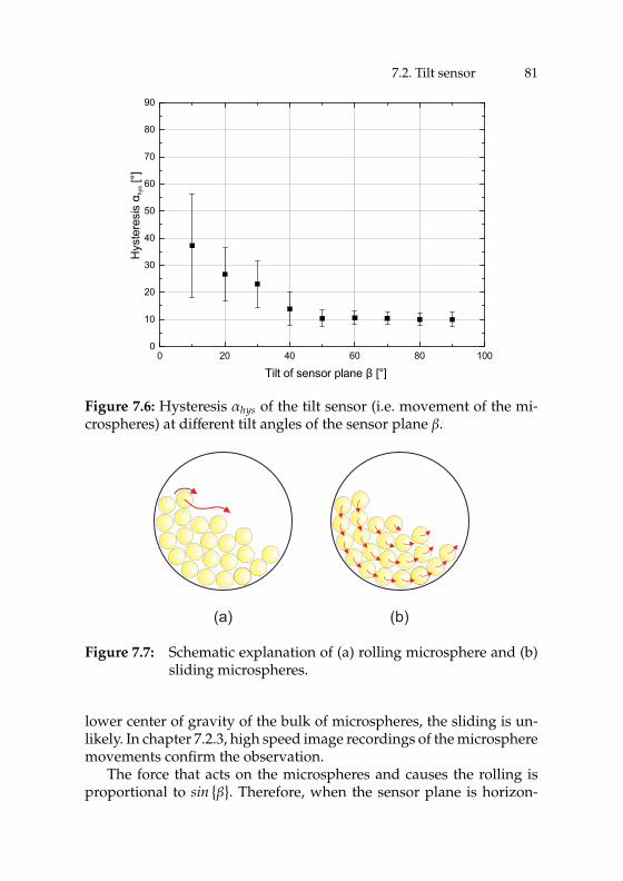
7.2. Tilt sensor 81
0 20 40 60 80 100
Tilt of sensor plane β [°]
0
10
20
30
40
50
60
70
80
90
Hys
tere
sis α
[°]
hys
Figure 7.6: Hysteresis αhys of the tilt sensor (i.e. movement of the mi-crospheres) at different tilt angles of the sensor plane β.
(a) (b)
Figure 7.7: Schematic explanation of (a) rolling microsphere and (b)sliding microspheres.
lower center of gravity of the bulk of microspheres, the sliding is un-likely. In chapter 7.2.3, high speed image recordings of the microspheremovements confirm the observation.
The force that acts on the microspheres and causes the rolling isproportional to sin
β
. Therefore, when the sensor plane is horizon-
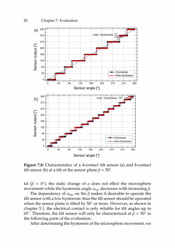
82 Chapter 7: Evaluation
0 45 90 135 180 225 270 315 3600
45
90
135
180
225
270
315
360
ClockwiseAnti-clockwise
Sen
sor o
utpu
t [°]
Sensor angle [°]
a)max. hysteresis: 8°
b)
0 45 90 135 180 225 270 315 3600
45
90
135
180
225
270
315
360
Sen
sor o
utpu
t [°]
Sensor angle [°]
ClockwiseAnti-clockwise
max. hysteresis: 10°
Figure 7.8: Characteristics of a 4-contact tilt sensor (a) and 8-contacttilt sensor (b) at a tilt of the sensor plane β = 50.
tal (β = 0), the static change of α does not effect the microspheremovement while the hysteresis angle αhys decreases with increasing β.
The dependency of αhys on the β makes it desirable to operate thetilt sensor with a low hysteresis: thus the tilt sensor should be operatedwhen the sensor plane is tilted by 50 or more. However, as shown inchapter 5.1, the electrical contact is only reliable for tilt angles up to65. Therefore, the tilt sensor will only be characterized at β = 50 inthe following parts of the evaluation.
After determining the hysteresis of the microsphere movement, we
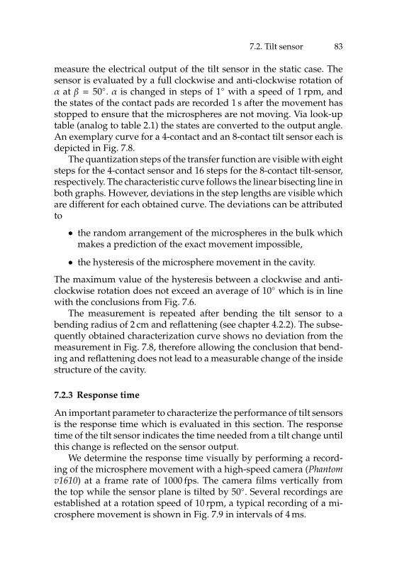
7.2. Tilt sensor 83
measure the electrical output of the tilt sensor in the static case. Thesensor is evaluated by a full clockwise and anti-clockwise rotation ofα at β = 50. α is changed in steps of 1 with a speed of 1 rpm, andthe states of the contact pads are recorded 1 s after the movement hasstopped to ensure that the microspheres are not moving. Via look-uptable (analog to table 2.1) the states are converted to the output angle.An exemplary curve for a 4-contact and an 8-contact tilt sensor each isdepicted in Fig. 7.8.
The quantization steps of the transfer function are visible with eightsteps for the 4-contact sensor and 16 steps for the 8-contact tilt-sensor,respectively. The characteristic curve follows the linear bisecting line inboth graphs. However, deviations in the step lengths are visible whichare different for each obtained curve. The deviations can be attributedto
• the random arrangement of the microspheres in the bulk whichmakes a prediction of the exact movement impossible,
• the hysteresis of the microsphere movement in the cavity.
The maximum value of the hysteresis between a clockwise and anti-clockwise rotation does not exceed an average of 10 which is in linewith the conclusions from Fig. 7.6.
The measurement is repeated after bending the tilt sensor to abending radius of 2 cm and reflattening (see chapter 4.2.2). The subse-quently obtained characterization curve shows no deviation from themeasurement in Fig. 7.8, therefore allowing the conclusion that bend-ing and reflattening does not lead to a measurable change of the insidestructure of the cavity.
7.2.3 Response time
An important parameter to characterize the performance of tilt sensorsis the response time which is evaluated in this section. The responsetime of the tilt sensor indicates the time needed from a tilt change untilthis change is reflected on the sensor output.
We determine the response time visually by performing a record-ing of the microsphere movement with a high-speed camera (Phantomv1610) at a frame rate of 1000 fps. The camera films vertically fromthe top while the sensor plane is tilted by 50. Several recordings areestablished at a rotation speed of 10 rpm, a typical recording of a mi-crosphere movement is shown in Fig. 7.9 in intervals of 4 ms.
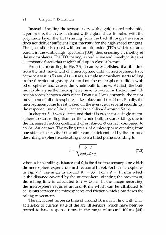
84 Chapter 7: Evaluation
Instead of sealing the sensor cavity with a gold-coated polyimidelayer on top, the cavity is closed with a glass slide. If sealed with thepolyimide layer, the LED shining from the back through the sensordoes not deliver sufficient light intensity for the high-speed imaging.The glass slide is coated with indium tin oxide (ITO) which is trans-parent in the visible light spectrum [109], thus ensuring a visibility ofthe microspheres. The ITO coating is conductive and thereby mitigateselectrostatic forces that might build up in glass substrate.
From the recording in Fig. 7.9, it can be established that the timefrom the first movement of a microsphere until all microspheres havecome to a rest, is 53 ms. At t = 0 ms, a single microsphere starts rollingin the direction of gravity. At t = 4 ms the microsphere collides withother spheres and causes the whole bulk to move. At first, the bulkmoves slowly as the microspheres have to overcome friction and ad-hesion forces between each other. From t = 16 ms onwards, the majormovement of all microspheres takes place until t = 44 ms. Finally, themicrospheres come to rest. Based on the average of several recordings,the response time of the tilt sensor is established around 50 ms.
In chapter 5, it was determined that it is easier for a single micro-sphere to start rolling than for the whole bulk to start sliding, due tothe increased friction coefficient of an Au-SU-8 contact compared toan Au-Au contact. The rolling time t of a microsphere crossing fromone side of the cavity to the other can be determined by the formuladescribing a sphere accelerating down a tilted plane according to
t =
√
2 · dsin(βd) · g (7.3)
where d is the rolling distance and βd is the tilt of the sensor plane whichthe microsphere experiences in direction of travel. For the microspheresin Fig. 7.9, this angle is around βd = 35. For a d = 1.5 mm whichis the distance covered by the microsphere initiating the movement,the rolling time is calculated to t = 23 ms. In the image recording,the microsphere requires around 40 ms which can be attributed tocollisions between the microspheres and friction which slow down therolling movement.
The measured response time of around 50 ms is in line with char-acteristics of current state of the art tilt sensors, which have been re-ported to have response times in the range of around 100 ms [44].
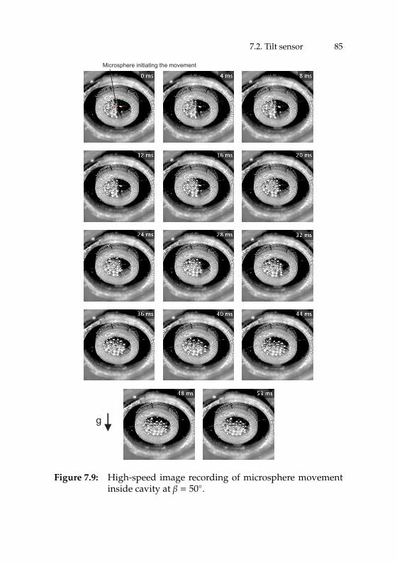
7.2. Tilt sensor 85
g
Microsphere initiating the movement
Figure 7.9: High-speed image recording of microsphere movementinside cavity at β = 50.
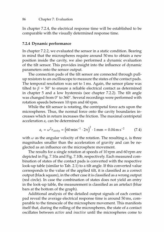
86 Chapter 7: Evaluation
In chapter 7.2.4, the electrical response time will be established to becomparable with the visually determined response time.
7.2.4 Dynamic performance
In chapter 7.2.2, we evaluated the sensor in a static condition. Bearingin mind that the microspheres require around 50 ms to obtain a newposition inside the cavity, we also performed a dynamic evaluationof the tilt sensor. This provides insight into the influence of dynamicparameters onto the sensor output.
The connection pads of the tilt sensor are connected through pull-up resistors to an oscilloscope to measure the states of the contact pads.The temporal resolution was set to 1 ms. Again, the sensor plane wastilted to β = 50 to ensure a reliable electrical contact as determinedin chapter 5 and a low hysteresis (see chapter 7.2.2). The tilt anglewas changed from 0 to 360. Several recordings were performed withrotation speeds between 10 rpm and 60 rpm.
While the tilt sensor is rotating, the centripetal force acts upon themicrospheres. Thus, the normal force onto the cavity boundaries in-creases which in return increases the friction. The maximal centripetalacceleration ac can be determined to
ac = ω2rcavity =
(
60 min−1 · 2π)2· 1 mm = 0.04 m s−2 (7.4)
with ω as the angular velocity of the rotation. The resulting ac is threemagnitudes smaller than the acceleration of gravity and can be ne-glected as an influence on the microsphere movement.
The results for a single rotation at speeds of 10 rpm and 60 rpm aredepicted in Fig. 7.10a and Fig. 7.10b, respectively. Each measured com-bination of states of the contact pads is converted with the respectivelook-up table (similar to Tab. 2.1) to a tilt angle. If this converted valuecorresponds to the value of the applied tilt, it is classified as a correctoutput (black square), in the other case it is classified as a wrong output(red circle). In case the combination of states does not yield an entryin the look-up table, the measurement is classified as an artefact (bluebars at the bottom of the graph).
Additional analysis of the detailed output signals of each contactpad reveal the average electrical response time is around 50 ms, com-parable to the timescale of the microsphere movement. This manifestsitself that, during the rolling of the microspheres, the state of a contactoscillates between active and inactive until the microspheres come to
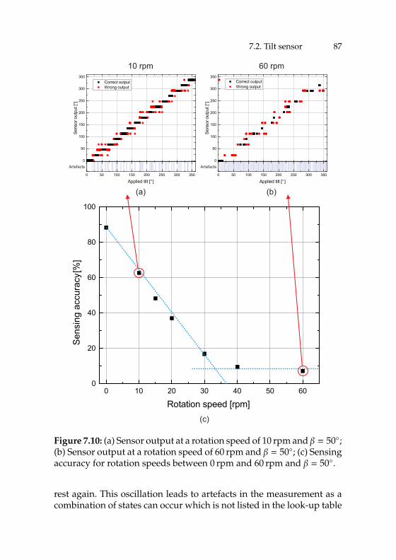
7.2. Tilt sensor 87
0 10 20 30 40 50 600
20
40
60
80
100
Sen
sing
acc
urac
y [%
]
Rotation speed [rpm]
(a) (b)
(c)
10 rpm 60 rpm
0
50
100
150
200
250
300
350 Correct output Wrong output
Sens
or o
utpu
t [°]
0 50 100 150 200 250 300 350
Applied tilt [° ]
Artefacts0
50
100
150
200
250
300
350 Correct output Wrong output
Sens
or o
utpu
t [°]
0 50 100 150 200 250 300 350
Applied tilt [° ]
Artefacts
Figure 7.10: (a) Sensor output at a rotation speed of 10 rpm and β = 50;(b) Sensor output at a rotation speed of 60 rpm and β = 50; (c) Sensingaccuracy for rotation speeds between 0 rpm and 60 rpm and β = 50.
rest again. This oscillation leads to artefacts in the measurement as acombination of states can occur which is not listed in the look-up table
88 Chapter 7: Evaluation
and can therefore not be classified.During the movement of the microspheres of 50 ms, the sensor
changes its tilt angle by around 3 at 10 rpm and by 18 at 60 rpm. As18 is larger than the hysteresis angle of 10, a rotation speed of 60 rpmkeeps the microspheres constantly rolling inside the cavity which leadsto measurement artefacts most of the time.
The amount of correctly measured tilt sensor outputs (blacksquares) is set into relation to the total number of acquired measure-ment points and defined as the sensing accuracy. Fig. 7.10c shows theresults for the sensing accuracy with respect to the applied rotationspeed. The sensing accuracy declines with increasing rotation speeduntil it reaches a saturation value of around 9 % for rotation speedshigher than 30 rpm. The linear decline of accuracy up to 30 rpm is dueto the increased relative amount of time that the microspheres spendrolling inside the cavity. With a microsphere movement time of 50 msand a hysteresis of 10 (see chapter 7.2.2), the microspheres are contin-uously moving for rotation speeds larger than 33 rpm. As the state ofa contact pad oscillates while microspheres are rolling across the pad,the contact pad states are not predictable, which makes the sensor out-put non-deterministic and results in a sensing accuracy of less than10 %.
The tilt sensor is best operated in static applications with no move-ment during the signal acquisition. If the sensor is operated in dy-namic conditions, a rotation speed of 20 rpm or an angular velocity of2.1 rad/min, respectively, should not be exceeded to achieve a correctoutput signal in more than 50 % of the acquisitions.
7.3 Conclusion
In this section we examined the characteristics of the tilt switch andtilt sensor. It was observed that the tilt switch has a make angle of5 and a break angle of 30. After bending to a radius of 5 cm andreflattening the sensor is still operational without changing the outputcharacteristics.
We identified that the tilt sensor should be operated at angles of thesensor plane β ≥ 50 to ensure a minimum in hysteresis. The examined4-contact and 8-contact tilt sensors exhibit a hysteresis of less than10 in the static states. The time scale of the microsphere movementsinside the cavity is around 50 ms which allows to operate the sensor atrotation speeds up to 20 rpm if an accuracy higher than 50 % is desired.
8Conclusion
A flexible tilt sensor was designed and evaluated. Different approaches forfabrication were presented. A comprehensive model of the sensor was intro-duced which provides insight on the influence of different design parameters.
An outlook discusses possible further improvements and applications of thetilt sensor concept.
90 Chapter 8: Conclusion
8.1 Summary and achievements
Research has covered different types of tilt sensors with varying sens-ing principles, achieving a wide range of possible tilt domains andresolutions, targeting specific applications. However, no tilt sensor hasbeen presented which is flexible and delivers a digital output signal.
In this thesis, we pursued the idea of a tilt sensor with microspheresas a pendulum, fabricated on plastic.
The major contributions of this thesis are the following:
• A flexible tilt sensor has been designed and fabricated on poly-imide foil, using standard clean room processes at temperaturesof less than 200 C. This allows the combination of the sensorwith other electronics and sensors on a single polyimide sub-strate which will enable future, more complex systems. This isa further step towards the development of completely flexible,wearable electronics which allow for new smart textiles, e.g. forhealth care.
• The use of microspheres with a diameter of 250µm as a pendu-lum was assessed, especially considering the contact mechanicswhich influence the performance of the microspheres. Here a bal-ance needs to be found between a reliable electrical contact andminimizing the adhesion forces of cavity and pendulum.
• A comprehensive model of the tilt sensor was developed andevaluated identifying important parameters for the sensor de-sign. The number of contact pads and the amount of micro-spheres in the cavity are the critical parameters which have adominant influence on the resolution and non-linearity.
• The characteristics of the tilt sensor concerning static behavioras well as the dynamics were evaluated. In order to reduce thesensor hysteresis to a minimum of 10, the sensor plane is tiltedby 50. The response time of the tilt sensor was identified. Asa result an application of the sensor in dynamic systems is notdesirable.
8.2 Scalability and limitations
The angular resolution of the tilt sensor is limited by the number ofcontact pads patterned on the substrate surface. An increase of the
8.3. Conclusions 91
number of contact pads with constant cavity radius however reducesthe area per contact pad in the cavity. With a cavity radius rcavity =
1000µm and for N ≥ 12 the width of the contact pads at the edge of thecavity is less than 250µm. In this case, a reliable electrical connection ofthe microsphere with the contact pad cannot be guaranteed. Therefore,for a number of contact pads N ≥ 12 the size of the cavity needs to beincreased to increase the width of the contact pad inside the cavity.
Alternatively, the diameter of the microspheres could be reduced.However, we have seen that for sphere diameters smaller than 250µmthe parasitic forces such as adhesion to the cavity wall dominate thegravitational forces, hindering a free movement of the microspheres.In addition, the reduced weight of the microsphere also creates lesspressure on the contact pads which has a negative influence on theelectrical contact with the contact pads.
The resolution of the sensor can be chosen according to the require-ments of the application, however an improved resolution requires alarger size of the sensor.
8.3 Conclusions
The following conclusions can be drawn from the results of this thesis:
• The non-linearity of the tilt sensor can be reduced to a minimumby selecting the amount of microspheres according to the size ofthe cavity and the number of contact pads. For an even numberof contact pads, the non-linearity is at a minimum when thependulum covers half of the area of the cavity.
• It is possible to fabricate a flexible tilt sensor using standard cleanroom processes.
• Reducing the size of the microspheres below a diameter of 250µmcomes to a limit because adhesion forces such as Van-der-Waalsforces start to dominate the gravitational forces. Equally, the pres-sure between microsphere and contact pad to create a reliableelectrical contact becomes marginal.
• The time scale of the microsphere movement inside the cavitydoes not allow to operate the sensor in highly dynamic applica-tions.
92 Chapter 8: Conclusion
8.4 Outlook
The sensing principle proved its functionality. Yet, we see a number ofareas where further development of the presented results can lead tonew application fields.
8.4.1 Materials and technology
Improvements in the materials and fabrication technology can enhancethe bendability of the sensor and further reduce the size of the sensingstructure.
We showed that the sensor is flexible and can be bent down to aradius of 2 cm with the SU-8 pillar structure. However, the height of thepillar structure combined with the epoxy glue increases the stiffnesssignificantly in the area of the sensing structure. This is a downsidefor an unobtrusive integration into textiles, where the stiffness is anegative factor.
By identifying alternative sealing chemicals, e.g. a silicone gluewhich has a lower Young’s modulus, the stiffness of the sensing struc-ture could be reduced and in return even allowed for a decreasedbending radius. The current sensing structure also consists of a doublering of SU-8 pillars with the outer ring used to apply the epoxy whileavoiding that the glue reaches the inner side of the cavity and interactswith the microspheres. While an alternative glue would be one optionfor improvement, other sealing and packaging approaches could bedeveloped to close the cavity and drop the outer ring of SU-8 pillars.This would allow to even further decrease the size of the tilt sensor,improving the unobtrusiveness.
A fabrication process which is performed entirely in a sealed en-vironment with no humidity is desirable to mitigate the build-up of awater film on the substrate and microsphere surface. We showed thatthis film reduces the operation range of the tilt sensor. By avoiding wetsurfaces, the tilt sensor operation range might be extended.
8.4.2 Sensor design
In this work, the focus for the cavity of the tilt sensor was always ona circular design with regularly arranged contact pads. This allowedto develop a comprehensive model of the tilt sensor and understandthe influence of the design parameters on the sensor performance.
8.4. Outlook 93
However, by modifying the arrangement of the contact pads and theshape of the cavity, we believe that the sensor can be optimized totarget specific applications.
The number of the contact pads on one side of the cavity can beincreased, leading to an increased resolution, while the other side ofthe cavity has a lower number of contact pads. The tilt sensor wouldthen offer a rough resolution with the sensor tilted in one direction andan improved resolution when tilted to the other direction.
The cavity wall of SU-8 pillars is structured by photolithography.This means, that arbitrary shapes of the cavity can be realized withthe appropriate lithography mask. The cavity can be not only circular,but also have e.g. areas that keep microspheres from rolling out of atrench again once they have rolled inside. Logistics use sensors witha cavity where a sphere rolls into trenches when tilted above a certainthreshold angle and so allow the indication of the maximum appliedtilt during the transport [110]. By combining this principle with our tiltsensor, a miniaturized, electronic version of this sensor can be realized.
8.4.3 Sensor readout
The readout of the tilt sensor has been performed by connecting thedevice with cables to a multimeter which defines the current state ofeach contact pad. With the respective look-up table these states arethen translated into the tilt angle. We see improvement possibilitiesregarding the state detection as well as the use of look-up table.
As one advantage of the tilt sensor, it does not require an activepower supply and for a readout merely the state of each contact padis important. Therefore, we envision a wireless passive readout of thesensor with a resonant circuit. Each contact pad is connected to a dif-ferent capacitance and all pads are then connected with a single coil.Depending on the state of the contact pads, the coil is electrically con-nected to a varying overall capacitance which leads to different reso-nance frequencies. This shift in resonance frequency of the LC resonantcircuit can be detected with respective equipment, even a readout viaNear Field Communication (NFC) with a smartphone can be possi-ble. Other wireless LC sensors have already been demonstrated, suchas humidity [111] or pressure sensors [112]. We have also shown aproof of concept by combining off-the-shelf tilt switches with RadioFrequency Identification (RFID) chips to build a die which can be readout wirelessly [113].

94 Chapter 8: Conclusion
The use of a look-up table could be replaced by the applicationof respective algorithms. When evaluating the dynamics of the tiltsensor, we noticed that during the movement of the microspheres theydo not reliably connect with the contact pads. This leads to undefinedstates in the sensor output which are not listed in the look-up table.By developing an appropriate algorithm, these undefined states couldalso be translated into a respective tilt angle, mitigating a missing activestate of the tilt sensor. This would improve the sensor performance ina dynamic environment and decrease the number of motion artefacts.
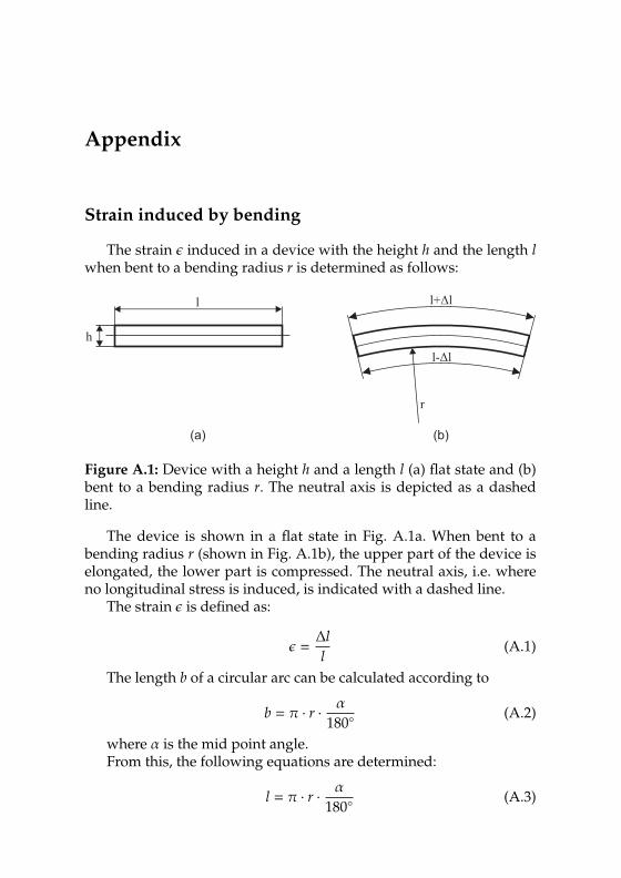
Appendix
Strain induced by bending
The strain ǫ induced in a device with the height h and the length lwhen bent to a bending radius r is determined as follows:
h
l
r
l-Δl
l+Δl
(a) (b)
Figure A.1: Device with a height h and a length l (a) flat state and (b)bent to a bending radius r. The neutral axis is depicted as a dashedline.
The device is shown in a flat state in Fig. A.1a. When bent to abending radius r (shown in Fig. A.1b), the upper part of the device iselongated, the lower part is compressed. The neutral axis, i.e. whereno longitudinal stress is induced, is indicated with a dashed line.
The strain ǫ is defined as:
ǫ =∆l
l(A.1)
The length b of a circular arc can be calculated according to
b = π · r · α180
(A.2)
where α is the mid point angle.From this, the following equations are determined:
l = π · r · α180
(A.3)
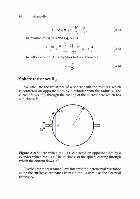
96 Appendix
l + ∆l = π ·(
r +h
2
)
· α180
(A.4)
The relation of Eq. A.3 and Eq. A.4 is
l + ∆l
l=π ·
(
r + h2
)
· α180
π · r · α180= 1 +
h
2r(A.5)
The left side of Eq. A.5 simplifies to 1 + ǫ, therefore
ǫ =h
2r(A.6)
Sphere resistance Rsp
We calculate the resistance of a sphere with the radius r whichis contacted on opposite sides by a cylinder with the radius a. Thecurrent flows only through the coating of the microsphere which hasa thickness h.
h
r
2a
x
b
Figure A.2: Sphere with a radius r, contacted on opposite sides by acylinder with a radius a. The thickness of the sphere coating throughwhich the current flows is h.
To calculate the resistance R, we integrate the incremental resistancealong the surface coordinate x from a to πr − a with ρ as the electricalresistivity.
97
R =
πr−a∫
a
ρ
U(x) · hdx (A.7)
The diameter b(x) at a given value of x can be determined by
b(x) = 2sin(
x
r
)
r. (A.8)
The circumference U(x) is then calculated according to
U(x) = b(x)π = 2πrsin(
x
r
)
. (A.9)
With Eq. A.9, Eq. A.7 equates to
R =
πr−a∫
a
ρ
2πrsin(
xr
)
· hdx
=ρ
2πhr
πr−a∫
a
1
sin(
xr
)dx
(A.10)
The integral is determined to∫
1
sin(
xr
)dx =[
r · ln(
tan(
x
2r
))]
(A.11)
With Eq. A.11 in Eq. A.10, we determine the resistance to
R =ρ
2πh
[
ln(
tan(
x
2r
))]πr−a
a(A.12)

98 Appendix
Bibliography
[1] K. Cherenack, T. Kinkeldei, C. Zysset, and G. Tröster, “Wo-ven thin-film metal interconnects,” IEEE Electron Device Letters,vol. 31, no. 7, pp. 740–742, 2010.
[2] Y. Moser and M. Gijs, “Miniaturized flexible temperature sen-sor,” Journal of Microelectromechanical Systems, vol. 16, no. 6, pp.1349–1354, 2007.
[3] S. C. Mannsfeld, B. C. Tee, R. M. Stoltenberg, C. V. H. Chen,S. Barman, B. V. Muir, A. N. Sokolov, C. Reese, and Z. Bao,“Highly sensitive flexible pressure sensors with microstructuredrubber dielectric layers,” Nature materials, vol. 9, no. 10, pp. 859–864, 2010.
[4] T. Kinkeldei, C. Zysset, N. Münzenrieder, and G. Tröster, “Anelectronic nose on flexible substrates integrated into a smart tex-tile,” Sensors and Actuators B: Chemical, vol. 174, pp. 81–86, 2012.
[5] N. Münzenrieder, K. Cherenack, and G. Tröster, “The effects ofmechanical bending and illumination on the performance of flex-ible igzo tfts,” Electron Devices, IEEE Transactions on, vol. 58, no. 7,pp. 2041–2048, July 2011.
[6] J. Seiter, S. Feese, B. Arnrich, G. Tröster, O. Amft, L. Macrea, andK. Maurer, “Activity monitoring in daily life as an outcome mea-sure for surgical pain relief intervention using smartphones,” inProceedings of the 17th annual international symposium on Interna-tional symposium on wearable computers, 2013, pp. 127–128.
[7] S.-W. Lee and K. Mase, “Activity and location recognition usingwearable sensors,” Pervasive Computing, IEEE, vol. 1, no. 3, pp.24–32, 2002.
[8] C. Strohrmann, H. Harms, C. Kappeler-Setz, and G. Tröster,“Monitoring kinematic changes with fatigue in running usingbody-worn sensors,” IEEE Transactions on Information Technologyin Biomedicine, vol. 16, no. 5, pp. 938–990, 2012.
100 Bibliography
[9] H. Harms, O. Amft, and G. Tröster, “Wearable therapist: sens-ing garments for supporting children improve posture,” in 11thInternational Conference on Ubiquitous Computing, Ubicomp 2009,2009.
[10] R. Hyde, L. Ketteringham, S. Neild, and R. Jones, “Estimationof upper-limb orientation based on accelerometer and gyro-scope measurements,” IEEE Transactions on Biomedical Engineer-ing, vol. 55, no. 2, pp. 746–754, Feb 2008.
[11] H. Gjoreski, M. Lustrek, and M. Gams, “Accelerometer place-ment for posture recognition and fall detection,” in 2011 7thInternational Conference on Intelligent Environments (IE), 2011, pp.47–54.
[12] S. Sukkarieh, P. Gibbens, B. Grocholsky, K. Willis, and H. F.Durrant-Whyte, “A low-cost, redundant inertial measurementunit for unmanned air vehicles,” The International Journal ofRobotics Research, vol. 19, no. 11, pp. 1089–1103, 2000.
[13] T. Toriyama and S. Sugiyama, “Analysis of piezoresistance in p-type silicon for mechanical sensors,” Microelectromechanical Sys-tems, Journal of, vol. 11, no. 5, pp. 598–604, 2002.
[14] S. Huang, X. Li, Z. Song, Y. Wang, H. Yang, L. Che, and J. Jiao, “Ahigh-performance micromachined piezoresistive accelerometerwith axially stressed tiny beams,” Journal of Micromechanics andMicroengineering, vol. 15, no. 5, p. 993, 2005.
[15] H. Chen, M. Bao, H. Zhu, and S. Shen, “A piezoresistive ac-celerometer with a novel vertical beam structure,” Sensors andActuators A: Physical, vol. 63, no. 1, pp. 19 – 25, 1997.
[16] A. Partridge, J. Reynolds, B. Chui, E. Chow, A. Fitzgerald,L. Zhang, N. I. Maluf, and T. Kenny, “A high-performanceplanar piezoresistive accelerometer,” Microelectromechanical Sys-tems, Journal of, vol. 9, no. 1, pp. 58–66, 2000.
[17] R. Amarasinghe, D. V. Dao, T. Toriyama, and S. Sugiyama,“Development of miniaturized 6-axis accelerometer utilizingpiezoresistive sensing elements,” Sensors and Actuators A: Physi-cal, vol. 134, no. 2, pp. 310 – 320, 2007.
Bibliography 101
[18] J. Sim, D. Kim, Y. Bae, K. Nam, and J. Lee, “Six-beam piezore-sistive accelerometer with self-cancelling cross-axis sensitivity,”Electronics Letters, vol. 34, no. 5, pp. 497–499, Mar 1998.
[19] A. R. Atwell, R. S. Okojie, K. T. Kornegay, S. L. Roberson, andA. Beliveau, “Simulation, fabrication and testing of bulk micro-machined 6h-sic high-g piezoresistive accelerometers,” Sensorsand Actuators A: Physical, vol. 104, no. 1, pp. 11 – 18, 2003.
[20] H. Luo, G. Zhang, L. Carley, and G. Fedder, “A post-cmos micro-machined lateral accelerometer,” Microelectromechanical Systems,Journal of, vol. 11, no. 3, pp. 188–195, 2002.
[21] J. Chae, H. Kulah, and K. Najafi, “A monolithic three-axis micro-gmicromachined silicon capacitive accelerometer,” Journal of Mi-croelectromechanical Systems, vol. 14, no. 2, pp. 235–242, 2005.
[22] C.-M. Sun, M.-H. Tsai, Y.-C. Liu, and W. Fang, “Implementationof a monolithic single proof-mass tri-axis accelerometer usingcmos-mems technique,” IEEE Transactions on Electron Devices,vol. 57, no. 7, pp. 1670–1679, 2010.
[23] I. Gönenli, Z. Celik-Butler, and D. Butler, “Surface microma-chined mems accelerometers on flexible polyimide substrate,”IEEE Sensors Journal, vol. 11, no. 10, pp. 2318–2326, 2011.
[24] F. Mailly, A. Giani, A. Martinez, R. Bonnot, P. Temple-Boyer, andA. Boyer, “Micromachined thermal accelerometer,” Sensors andActuators A: Physical, vol. 103, no. 3, pp. 359 – 363, 2003.
[25] U. Mescheder and S. Majer, “Micromechanical inclinometer,”Sensors and Actuators A: Physical, vol. 60, no. 1, pp. 134 – 138,1997.
[26] L. Tang, K. Zhang, S. Chen, G. Zhang, and G. Liu, “MEMS in-clinometer based on a novel piezoresistor structure,” Microelec-tronics Journal, vol. 40, no. 1, pp. 78 – 82, 2009.
[27] C. Smith, A. Villanueva, and S. Priya, “Aurelia aurita bio-inspired tilt sensor,” Smart Materials and Structures, vol. 21, no. 10,p. 105015, 2012.
[28] C. H. Lee and S. S. Lee, “Capacitive tilt sensor using metallicball,” in Proceedings of ASME 2009 International Mechanical Engi-neering Congress and Exposition, vol. 12, 2009, pp. 445–448.
102 Bibliography
[29] J. Liang, F. Kohsaka, X. Li, K. Kunitomo, and T. Ueda, “Charac-terization of a quarts MEMS tilt sensor with 0 001 precision,” inInternational Solid-State Sensors, Actuators and Microsystems Con-ference, 2009. TRANSDUCERS 2009., 2009, pp. 308–310.
[30] L. Zhao and E. Yeatman, “Micro capacitive tilt sensor for hu-man body movement detection,” in 4th International Workshopon Wearable and Implantable Body Sensor Networks (BSN 2007), ser.IFMBE Proceedings, S. Leonhardt, T. Falck, and P. Mähönen, Eds.Springer Berlin Heidelberg, 2007, vol. 13, pp. 195–200.
[31] R. Olaru and D. Dragoi, “Inductive tilt sensor with magnets andmagnetic fluid,” Sensors and Actuators A: Physical, vol. 120, no. 2,pp. 424–428, 2005.
[32] L. Rovati and S. Cattini, “Contactless two-axis inclination mea-surement system using planar flux-gate sensor,” IEEE Transac-tions on Instrumentation and Measurement, vol. 59, no. 5, pp. 1284–1293, 2010.
[33] T. G. Constandinou and J. Georgiou, “Micro-optoelectromechanical tilt sensor,” Journal of Sensors, vol.2008, 2008.
[34] J.-H. Wu, K.-Y. Horng, S.-L. Lin, and R.-S. Chang, “A two-axistilt sensor based on optics,” Measurement Science and Technology,vol. 17, no. 4, p. N9, 2006.
[35] L. Amaral, O. Frazao, J. Santos, and A. Ribeiro, “Fiber-optic incli-nometer based on taper michelson interferometer,” IEEE SensorsJournal, vol. 11, no. 9, pp. 1811–1814, 2011.
[36] O. Frazao, R. Falate, J. L. Fabris, J. L. Santos, L. A. Ferreira, andF. M. Araújo, “Optical inclinometer based on a single long-periodfiber grating combined with a fused taper,” Optics Letters, vol. 31,no. 20, pp. 2960–2962, 2006.
[37] L.-Y. Shao and J. Albert, “Compact fiber-optic vector inclinome-ter,” Optics Letters, vol. 35, no. 7, pp. 1034–1036, 2010.
[38] B.-O. Guan, H.-Y. Tam, and S.-Y. Liu, “Temperature-independentfiber bragg grating tilt sensor,” IEEE Photonics Technology Letters,vol. 16, no. 1, pp. 224–226, 2004.
Bibliography 103
[39] X. Dong, C. Zhan, K. Hu, P. Shum, and C. C. Chan, “Temperature-insensitive tilt sensor with strain-chirped fiber bragg gratings,”IEEE Photonics Technology Letters, vol. 17, no. 11, pp. 2394–2396,2005.
[40] B.-J. Peng, Y. Zhao, Y. Zhao, and J. Yang, “Tilt sensor with fbgtechnology and matched fbg demodulating method,” IEEE Sen-sors Journal, vol. 6, no. 1, pp. 63–66, 2006.
[41] H. Bao, X. Dong, L.-Y. Shao, C.-L. Zhao, and S. Jin, “Temperature-insensitive 2-d tilt sensor by incorporating fiber bragg grat-ings with a hybrid pendulum,” Optics Communications, vol. 283,no. 24, pp. 5021–5024, 2010.
[42] J. H. Lee and S. S. Lee, “Electrolytic tilt sensor fabricated byusing electroplating process,” Sensors and Actuators A: Physical,vol. 167, no. 1, pp. 1–7, 2011.
[43] H. Jung, C. J. Kim, and S. H. Kong, “An optimized MEMS-basedelectrolytic tilt sensor,” Sensors and Actuators A: Physical, vol. 139,no. 1 - 2, pp. 23–30, 2007.
[44] J. C. Choi, Y. C. Choi, J. K. Lee, and S. H. Kong, “Miniatur-ized dual-axis electrolytic tilt sensor,” Japanese Journal of AppliedPhysics, vol. 51, no. 6, p. 06FL13, 2012.
[45] W. Bin, M. M. Hossain, and S. H. Kong, “Pdms-based two-axisinclinometer with a 360-degree measuring range,” Sensors andActuators A: Physical, vol. 239, pp. 54–60, 2016.
[46] R. A. Yotter, R. R. Baxter, S. Ohno, S. D. Hawley, and D. M. Wil-son, “On a micromachined fluidic inclinometer,” in 12th Interna-tional Conference on Solid-State Sensors, Actuators and Microsystems(TRANSDUCERS), vol. 2, 2003, pp. 1279–1282.
[47] A. B. A. Manaf, K. Nakamura, and Y. Matsumoto, “Characteri-zation of miniaturized one-side-electrode-type fluid-based incli-nometer,” Sensors and Actuators A: Physical, vol. 144, no. 1, pp.74–82, 2008.
[48] B. Salvador, A. Luque, and J. M. Quero, “Microfluidic capacitivetilt sensor using pcb-mems,” in 2015 IEEE International Conferenceon Industrial Technology (ICIT), 2015, pp. 3356–3360.
104 Bibliography
[49] H. Ueda, H. Ueno, K. Itoigawa, and T. Hattori, “Micro capaci-tive inclination sensor utilizing dielectric nano-particles,” in 19thIEEE International Conference on Micro Electro Mechanical Systems(MEMS), 2006, pp. 706–709.
[50] D. Benz, T. Botzelmann, H. Kück, and D. Warkentin, “On low costinclination sensors made from selectively metallized polymer,”Sensors and Actuators A: Physical, vol. 123-124, no. 0, pp. 18–22,2005.
[51] O. Baltag, D. Costandache, and A. Salceanu, “Tilt measurementsensor,” Sensors and Actuators A: Physical, vol. 81, no. 1 - 3, pp.336–339, 2000.
[52] B. Ando, A. Ascia, and S. Baglio, “A ferrofluidic inclinometer inthe resonant configuration,” IEEE Transactions on Instrumentationand Measurement, vol. 59, no. 3, pp. 558–564, 2010.
[53] D. Welch, J. Georgiou, and J. B. Christen, “Fully differentialcurrent-mode MEMS dual-axis optical inclination sensor,” Sen-sors and Actuators A: Physical, vol. 192, no. 0, pp. 133 – 139, 2013.
[54] J. S. Bajic, D. Z. Stupar, L. M. Manojlovic, M. P. Slankamenac, andM. B. Zivanov, “A simple, low-cost, high-sensitivity fiber-optictilt sensor,” Sensors and Actuators A: Physical, vol. 185, no. 0, pp.33–38, 2012.
[55] X. Zhang, K. Ni, C. Zhao, M. Ye, and Y. Jin, “Tilt sensor basedon intermodal photonic crystal fiber interferometer,” PhotonicSensors, vol. 4, no. 3, pp. 209–214, 2014.
[56] J. Courteaud, P. Combette, N. Crespy, G. Cathebras, and A. Gi-ani, “Thermal simulation and experimental results of a microma-chined thermal inclinometer,” Sensors and Actuators A: Physical,vol. 141, no. 2, pp. 307–313, 2008.
[57] S. Billat, H. Glosch, M. Kunze, F. Hedrich, J. Frech, J. Auber,W. Lang, H. Sandmaier, and W. Wimmer, “Convection-basedmicromachined inclinometer using SOI technology,” in The 14thIEEE International Conference on Micro Electro Mechanical Systems(MEMS), 2001, pp. 159–161.
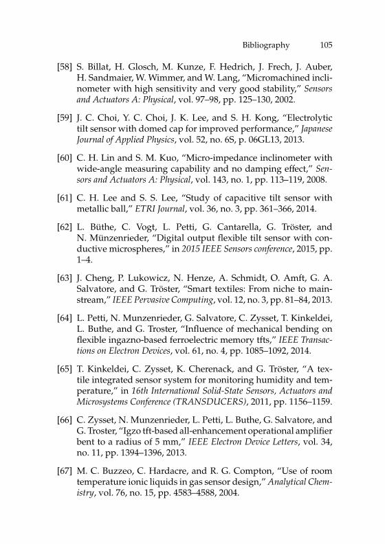
Bibliography 105
[58] S. Billat, H. Glosch, M. Kunze, F. Hedrich, J. Frech, J. Auber,H. Sandmaier, W. Wimmer, and W. Lang, “Micromachined incli-nometer with high sensitivity and very good stability,” Sensorsand Actuators A: Physical, vol. 97–98, pp. 125–130, 2002.
[59] J. C. Choi, Y. C. Choi, J. K. Lee, and S. H. Kong, “Electrolytictilt sensor with domed cap for improved performance,” JapaneseJournal of Applied Physics, vol. 52, no. 6S, p. 06GL13, 2013.
[60] C. H. Lin and S. M. Kuo, “Micro-impedance inclinometer withwide-angle measuring capability and no damping effect,” Sen-sors and Actuators A: Physical, vol. 143, no. 1, pp. 113–119, 2008.
[61] C. H. Lee and S. S. Lee, “Study of capacitive tilt sensor withmetallic ball,” ETRI Journal, vol. 36, no. 3, pp. 361–366, 2014.
[62] L. Büthe, C. Vogt, L. Petti, G. Cantarella, G. Tröster, andN. Münzenrieder, “Digital output flexible tilt sensor with con-ductive microspheres,” in 2015 IEEE Sensors conference, 2015, pp.1–4.
[63] J. Cheng, P. Lukowicz, N. Henze, A. Schmidt, O. Amft, G. A.Salvatore, and G. Tröster, “Smart textiles: From niche to main-stream,” IEEE Pervasive Computing, vol. 12, no. 3, pp. 81–84, 2013.
[64] L. Petti, N. Munzenrieder, G. Salvatore, C. Zysset, T. Kinkeldei,L. Buthe, and G. Troster, “Influence of mechanical bending onflexible ingazno-based ferroelectric memory tfts,” IEEE Transac-tions on Electron Devices, vol. 61, no. 4, pp. 1085–1092, 2014.
[65] T. Kinkeldei, C. Zysset, K. Cherenack, and G. Tröster, “A tex-tile integrated sensor system for monitoring humidity and tem-perature,” in 16th International Solid-State Sensors, Actuators andMicrosystems Conference (TRANSDUCERS), 2011, pp. 1156–1159.
[66] C. Zysset, N. Munzenrieder, L. Petti, L. Buthe, G. Salvatore, andG. Troster, “Igzo tft-based all-enhancement operational amplifierbent to a radius of 5 mm,” IEEE Electron Device Letters, vol. 34,no. 11, pp. 1394–1396, 2013.
[67] M. C. Buzzeo, C. Hardacre, and R. G. Compton, “Use of roomtemperature ionic liquids in gas sensor design,” Analytical Chem-istry, vol. 76, no. 15, pp. 4583–4588, 2004.
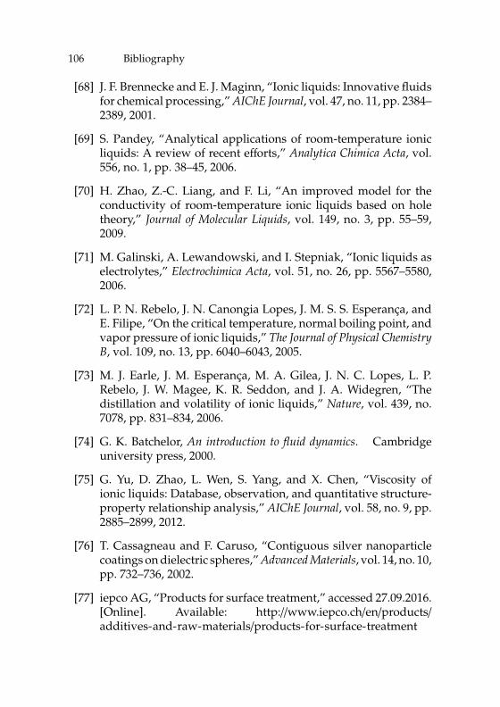
106 Bibliography
[68] J. F. Brennecke and E. J. Maginn, “Ionic liquids: Innovative fluidsfor chemical processing,” AIChE Journal, vol. 47, no. 11, pp. 2384–2389, 2001.
[69] S. Pandey, “Analytical applications of room-temperature ionicliquids: A review of recent efforts,” Analytica Chimica Acta, vol.556, no. 1, pp. 38–45, 2006.
[70] H. Zhao, Z.-C. Liang, and F. Li, “An improved model for theconductivity of room-temperature ionic liquids based on holetheory,” Journal of Molecular Liquids, vol. 149, no. 3, pp. 55–59,2009.
[71] M. Galinski, A. Lewandowski, and I. Stepniak, “Ionic liquids aselectrolytes,” Electrochimica Acta, vol. 51, no. 26, pp. 5567–5580,2006.
[72] L. P. N. Rebelo, J. N. Canongia Lopes, J. M. S. S. Esperança, andE. Filipe, “On the critical temperature, normal boiling point, andvapor pressure of ionic liquids,” The Journal of Physical ChemistryB, vol. 109, no. 13, pp. 6040–6043, 2005.
[73] M. J. Earle, J. M. Esperança, M. A. Gilea, J. N. C. Lopes, L. P.Rebelo, J. W. Magee, K. R. Seddon, and J. A. Widegren, “Thedistillation and volatility of ionic liquids,” Nature, vol. 439, no.7078, pp. 831–834, 2006.
[74] G. K. Batchelor, An introduction to fluid dynamics. Cambridgeuniversity press, 2000.
[75] G. Yu, D. Zhao, L. Wen, S. Yang, and X. Chen, “Viscosity ofionic liquids: Database, observation, and quantitative structure-property relationship analysis,” AIChE Journal, vol. 58, no. 9, pp.2885–2899, 2012.
[76] T. Cassagneau and F. Caruso, “Contiguous silver nanoparticlecoatings on dielectric spheres,” Advanced Materials, vol. 14, no. 10,pp. 732–736, 2002.
[77] iepco AG, “Products for surface treatment,” accessed 27.09.2016.[Online]. Available: http://www.iepco.ch/en/products/additives-and-raw-materials/products-for-surface-treatment
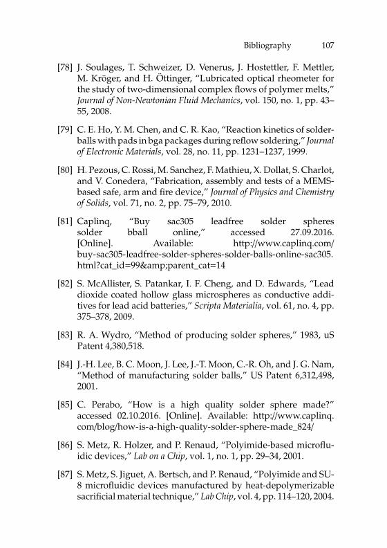
Bibliography 107
[78] J. Soulages, T. Schweizer, D. Venerus, J. Hostettler, F. Mettler,M. Kröger, and H. Öttinger, “Lubricated optical rheometer forthe study of two-dimensional complex flows of polymer melts,”Journal of Non-Newtonian Fluid Mechanics, vol. 150, no. 1, pp. 43–55, 2008.
[79] C. E. Ho, Y. M. Chen, and C. R. Kao, “Reaction kinetics of solder-balls with pads in bga packages during reflow soldering,” Journalof Electronic Materials, vol. 28, no. 11, pp. 1231–1237, 1999.
[80] H. Pezous, C. Rossi, M. Sanchez, F. Mathieu, X. Dollat, S. Charlot,and V. Conedera, “Fabrication, assembly and tests of a MEMS-based safe, arm and fire device,” Journal of Physics and Chemistryof Solids, vol. 71, no. 2, pp. 75–79, 2010.
[81] Caplinq, “Buy sac305 leadfree solder spheressolder bball online,” accessed 27.09.2016.[Online]. Available: http://www.caplinq.com/buy-sac305-leadfree-solder-spheres-solder-balls-online-sac305.html?cat_id=99&parent_cat=14
[82] S. McAllister, S. Patankar, I. F. Cheng, and D. Edwards, “Leaddioxide coated hollow glass microspheres as conductive addi-tives for lead acid batteries,” Scripta Materialia, vol. 61, no. 4, pp.375–378, 2009.
[83] R. A. Wydro, “Method of producing solder spheres,” 1983, uSPatent 4,380,518.
[84] J.-H. Lee, B. C. Moon, J. Lee, J.-T. Moon, C.-R. Oh, and J. G. Nam,“Method of manufacturing solder balls,” US Patent 6,312,498,2001.
[85] C. Perabo, “How is a high quality solder sphere made?”accessed 02.10.2016. [Online]. Available: http://www.caplinq.com/blog/how-is-a-high-quality-solder-sphere-made_824/
[86] S. Metz, R. Holzer, and P. Renaud, “Polyimide-based microflu-idic devices,” Lab on a Chip, vol. 1, no. 1, pp. 29–34, 2001.
[87] S. Metz, S. Jiguet, A. Bertsch, and P. Renaud, “Polyimide and SU-8 microfluidic devices manufactured by heat-depolymerizablesacrificial material technique,” Lab Chip, vol. 4, pp. 114–120, 2004.
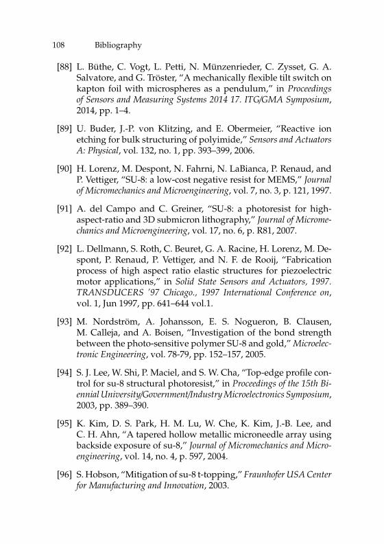
108 Bibliography
[88] L. Büthe, C. Vogt, L. Petti, N. Münzenrieder, C. Zysset, G. A.Salvatore, and G. Tröster, “A mechanically flexible tilt switch onkapton foil with microspheres as a pendulum,” in Proceedingsof Sensors and Measuring Systems 2014 17. ITG/GMA Symposium,2014, pp. 1–4.
[89] U. Buder, J.-P. von Klitzing, and E. Obermeier, “Reactive ionetching for bulk structuring of polyimide,” Sensors and ActuatorsA: Physical, vol. 132, no. 1, pp. 393–399, 2006.
[90] H. Lorenz, M. Despont, N. Fahrni, N. LaBianca, P. Renaud, andP. Vettiger, “SU-8: a low-cost negative resist for MEMS,” Journalof Micromechanics and Microengineering, vol. 7, no. 3, p. 121, 1997.
[91] A. del Campo and C. Greiner, “SU-8: a photoresist for high-aspect-ratio and 3D submicron lithography,” Journal of Microme-chanics and Microengineering, vol. 17, no. 6, p. R81, 2007.
[92] L. Dellmann, S. Roth, C. Beuret, G. A. Racine, H. Lorenz, M. De-spont, P. Renaud, P. Vettiger, and N. F. de Rooij, “Fabricationprocess of high aspect ratio elastic structures for piezoelectricmotor applications,” in Solid State Sensors and Actuators, 1997.TRANSDUCERS ’97 Chicago., 1997 International Conference on,vol. 1, Jun 1997, pp. 641–644 vol.1.
[93] M. Nordström, A. Johansson, E. S. Nogueron, B. Clausen,M. Calleja, and A. Boisen, “Investigation of the bond strengthbetween the photo-sensitive polymer SU-8 and gold,” Microelec-tronic Engineering, vol. 78-79, pp. 152–157, 2005.
[94] S. J. Lee, W. Shi, P. Maciel, and S. W. Cha, “Top-edge profile con-trol for su-8 structural photoresist,” in Proceedings of the 15th Bi-ennial University/Government/Industry Microelectronics Symposium,2003, pp. 389–390.
[95] K. Kim, D. S. Park, H. M. Lu, W. Che, K. Kim, J.-B. Lee, andC. H. Ahn, “A tapered hollow metallic microneedle array usingbackside exposure of su-8,” Journal of Micromechanics and Micro-engineering, vol. 14, no. 4, p. 597, 2004.
[96] S. Hobson, “Mitigation of su-8 t-topping,” Fraunhofer USA Centerfor Manufacturing and Innovation, 2003.
Bibliography 109
[97] T. Tamai, S. Sawada, and Y. Hattori, “Deformation of crystalstructure and distribution of mechanical stress in tin-plated layerunder contact loading,” in 2009 Proceedings of the 55th IEEE HolmConference on Electrical Contacts, 2009, pp. 162–167.
[98] P. G. Slade, Electrical contacts: principles and applications. CRCPress, 2013.
[99] B. H. Jang, P. H. Tseng, W. Fang, and S. W. Lin, “Extraction ofmicro-contact properties using a novel micromachined on-chipapparatus,” in 2008 International Conference on Electronic Materialsand Packaging, Oct 2008, pp. 285–288.
[100] C. Clay and A. Hodgson, “Water and mixed oh/water adsorptionat close packed metal surfaces,” Current Opinion in Solid State andMaterials Science, vol. 9, no. 1–2, pp. 11–18, 2005.
[101] A. Hodgson and S. Haq, “Water adsorption and the wetting ofmetal surfaces,” Surface Science Reports, vol. 64, no. 9, pp. 381–451,2009.
[102] H. Hertz, “Über die berührung fester elastischer körper,” Journalfür die reine und angewandte Mathematik, vol. 92, pp. 156–171, 1881.
[103] V. Popov, Contact mechanics and friction: physical principles andapplications. Springer Science & Business Media, 2010.
[104] J. Diao, K. Gall, and M. L. Dunn, “Surface-stress-induced phasetransformation in metal nanowires,” Nature materials, vol. 2,no. 10, pp. 656–660, 2003.
[105] L. Kondic, R. Hartley, S. Tennakoon, B. Painter, and R. Behringer,“Segregation by friction,” EPL (Europhysics Letters), vol. 61, no. 6,p. 742, 2003.
[106] E. Weisstein, “Circular segment - mathworld - a wolframweb resource,” accessed 17.09.2016. [Online]. Available:http://mathworld.wolfram.com/CircularSegment.html
[107] J. H. Conway and N. J. A. Sloane, Sphere packings, lattices andgroups. Springer Science & Business Media, 2013, vol. 290.
[108] L. Büthe, C. Vogt, L. Petti, G. Cantarella, N. Münzenrieder, andG. Tröster, “Fabrication, modeling and evaluation of a digital

110 Bibliography
output tilt sensor with conductive microspheres,” IEEE SensorsJournal, 2016, submitted.
[109] T. Minami, H. Sonohara, T. Kakumu, and S. Takata, “Physics ofvery thin ito conducting films with high transparency preparedby dc magnetron sputtering,” Thin Solid Films, vol. 270, no. 1, pp.37–42, 1995.
[110] Schockwatch, “Tilt indicators - shipping and handlingmonitoring devices,” accessed 17.09.2016. [Online]. Available:http://shockwatch.com/products/impact-and-tilt/tilt-indicators
[111] E. L. Tan, W. N. Ng, R. Shao, B. D. Pereles, and K. G. Ong, “Awireless, passive sensor for quantifying packaged food quality,”Sensors, vol. 7, no. 9, p. 1747, 2007.
[112] C. Li, Q. Tan, C. Xue, W. Zhang, Y. Li, and J. Xiong, “A high-performance lc wireless passive pressure sensor fabricated us-ing low-temperature co-fired ceramic (ltcc) technology,” Sensors,vol. 14, no. 12, pp. 23 337–23 347, 2014.
[113] L. Büthe, M. Hardegger, P. Brülisauer, and G. Tröster, “Rfid-die:Battery-free orientation sensing using an array of passive tiltswitches,” in Proceedings of the 2014 ACM International Joint Con-ference on Pervasive and Ubiquitous Computing: Adjunct Publication,2014, pp. 215–218.
Glossary
Notation Description Page ListAdisk Area of the microsphere disk 70Asphere Cross-section area of a microsphere 70E Young’s modulus 40, 52FN Normal force of microsphere on
substrate surface50, 56, 57
Find Indentation force 52I Second moment of area 40N Number of contact pads 60, 64, 66, 68–71Nspheres Amount of microspheres 60, 70, 71R Radius of microsphere 50, 52RC Constriction resistance 48RS Sharvin resistance 48, 49Rsp Sphere resistance 48, 50α Tilt angle of device 21, 64, 75, 78–
80, 82, 83αT Coefficient of thermal expansion 39αbreak Break angle of tilt switch 76αhys Hystersis angle of tilt sensor 80, 82αmake Make angle of tilt switch 75, 76αpad Angle of a single contact pad 60αres Angular resolution 60, 62, 71β Tilt angle of sensor plane 20, 78–80, 82δ Rotation angle of second rotation
axis78
δn Packing density 70ηdisk Ratio of microsphere disk height
and cavity radius67
ηpad Ratio of ground to contact pad 60, 67–69, 71γ Rotation angle of first rotation axis 78γlv Surface tension 26µk Kinematic friction coefficient 56µpad Representation of ηpad between 0
and 168
112 Glossary
Notation Description Page Listν Poisson ratio 52ω Angular velocity 86ρl Density of liquid 27θ Contact angle of liquid with solid
surface26
θi Central angles of contact andground pad to the horizontal
66, 67
ϕ Angle between horizontal and topof microsphere disk
67
ξstates Evaluation parameter describingthe non-linearity
62, 65–69
a Radius of a-spots 48, 49, 55ac Centripetal acceleration 86cdist Spacing between pillars 40–42cpillar Edge length of a pillar 40–42dcrit Critical penetration depth 54, 55dind Indentation depth 52h Height 27hdisk Height of microsphere disk 61, 66–71l f p Mean free path of electrons 49, 50rcavity Radius of sensor cavity 60, 65, 67, 70, 71rcontact Inner contact radius of contact pads 60, 66, 71
ADC Analog-to-digital converter 62AFM Atomic force microscopy 52–57Al Aluminum 35Au Gold 34, 35, 57, 84
CMOS Complementary metal-oxide semi-conductor
6
Cr Chrome 34, 35
DC Direct current 4
FBG Fiber bragg grating 6
Glossary 113
Notation Description Page List
GaInSn Gallium indium tin 7
HWA Healthcare, wellness and assistedliving
xiii
IL Ionic liquid 27ITO Indium tin oxide 84
LC Circuit with inductance and capac-itance forming a resonant circuit
93
LED Light emitting diode 6, 79, 84LFM Lateral force microscopy 56
MEMS Micro-electromechanical system 3, 22
N2 Nitrogen 51NaCl Sodium cloride 8, 27NFC Near Field Communication 93
O2 Oxygen 35, 40, 45OSA Optical spectrum analyzer 6
PC Personal computer 75, 79PCF Photonic crystal fiber 8PI Polyimide xiii, xv
RFID Radio Frequency Identification 93RIE Reactive ion etching 35, 40, 45, 50RMS Root mean square of surface rough-
ness53–55
SEM Scanning electron microscopy 29, 36, 42–44SF6 Sulfur hexafluoride 35Si Silicon 3, 57, 58

114 Glossary
Notation Description Page ListSMD Surface mount device 5SNR Signal to noise ratio 4
UV Ultra violett 39, 40
ZnO Zinc oxide 3


![Webinar SW Urich 02 08[1] › portal › pdf › sw-urich-webar-0208.pdf · assure superior utilization and bill rates. Client Relationship Opportunistic. No defined solution sets](https://img.pdfslide.net/doc/110x75/5f10ac8d7e708231d44a43ed/webinar-sw-urich-02-081-a-portal-a-pdf-a-sw-urich-webar-0208pdf-assure.jpg)