Embed Size (px)
Citation preview

Instruction Manual Model 177 Microvolt DMM
and Model 1788 Battery Pack
01978, Keithley Instruments. Inc. Cleveland, Ohio, U.S.A.
Document Number 29683
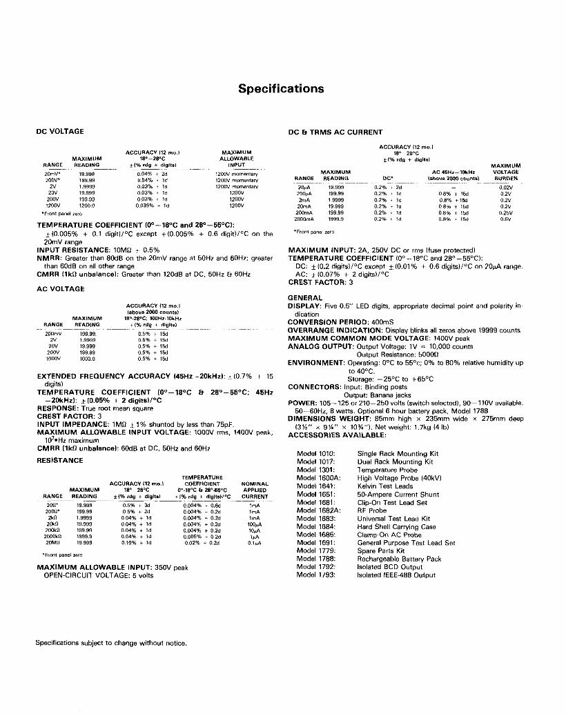
Specifications
TEMPERATTURE COEFFlClENT VT-WC and m-55T.I: *W305% + 0.1 di~itI/~C e~cepf *10.005% + 0.6 digifll°C on the
EXTENDED FREOUENCV ACCURACY ,45Hz--2OkW: i 10.7% + 15 diaitSl
TEtiPERATURE COEFFICIENT 10°-18pC Et ZW-55°C: --2OkHz,: * ~0.05% + 2 digifs,PC
RESPONSE: True mot mean squsre CREST FACTOR: 3 INPUT IMPEDANCE: IMO * 1% shunted by less than 75pF. MnlyMUM *uOWABLE INPUT “OLT*GE: 1000” rms. ,400”
lO’+b maximum CMRR Ilk0 unbalancel: SOdS at DC. 5OHz and SOHz
RESISTANCE
MAXIMVM ALLOWABLE INPUT: 350” peak OPEN-CIRCUIT VOLTAGE: 5 volts
45Hz
peak
MAXIMUM INPUT: 2A. 250” DC or rms lfuse protected, TEMPERATURE COEFFICIENT W-WC and 28D-550C,:
DC: f 10.2 digits)/°C except f 10.01% + 0.6 digitsl/“C on 2OpA range.
GENERAL DISPLAY: Five 0.5” LED digits, appropriate decimal point and polarity ins
dicatio” CONVERSION PERIOD: 400mS OVERRANGE INDICATION: Display blinks all zems above 19999 counts MAXlM”M COMMON MODE VOLTAGE: MOO” peak ANALOG OUTPUT: Output Voltage: IV = 10,000 county
Output Resistance: 50000 ENVIRONMENT: Operating: O’C to SYc; 0% to 80% relative humidih/ up
to ‘WC. storage: --25oc to ~+65T
CONNECTORS: In,,ut: Binding ,mst~ O”QJ”C smana jacks
POWER: IOS- 125 or 210-250 volts (switch selected), gOpllOV available. 506-6OHz. 8 warts. Optional 6 hour battery pack, Model 1788
DIMENSIONS WEIGHT: 85mm high x 235mm wide x 275mm deep 13%” x 9%” x 10%“). Net weight: l.,kg (4 lb,
ACCESSORlES *“VAILA.BLE:
Model ,010: Model ,017: Model ,301: Model 1SOOA: Model ,641: Model 1651: Model 1681: Model 1mzA: Model ,683: Model ,684: Model ,665: Model ,m,: Model ,779: Model 1788: Model 1792: Made, ,793:
Single Rack Mounfing Kif Dual Rack Mounting Kit Tempereture Probe High Voltage Probe 14OkVl Kelvin Test Leads 50-Ampere Current Shunt Clip-On Test Lead Set RF Probe Universal Test Lead Kit Hard Shell Carving Case Clamp~on AC Probe Genersl Purpose Test Lead Set Spare Paris Kit Rechargeable Battery Pack Isolated BCD OUtput lsalsted IEEE-488 Output
Specifications subject to change without notice.
TABLE OF CONTENTS
Paragraoh Title Pan.3
1.1 1.2 1.3 1.4 1.5 1.6 1.7 1.8 1.9 1.10 1.10.1 1.102 1.10.3 1.10.4 1.10.5
SECTION I-GENERAL INFORMATION Introduction ............................. Model 177 Features. ...................... Warranty Information ..................... ManualAddenda ......................... Safety Symbols and Terms. ................ Safety Precautions ....................... Specifications ........................... Unpacking and Inspection ................. Scope of Model 177 Instruction Manual ...... Optional Accessories. .....................
Power Options. ........................ Cables and Connectors. ................. Probes and Shunts ..................... Carrying Case and Rack Mount ........... Output Options ........................
......
......
......
......
......
......
......
......
......
......
......
......
......
......
......
l-l l-l 1-l 1-l 1-l 1-l
., 1-l 1-2
., ., l-2 1-2 1-2 1-2 1-2 l-2 1-2
2.1 2.2 2.3 2.4 2.5 2.6 2.7 2.8 2.9 2.10 2.11 2.12 2.13 2.14 2.15 2.16
3.1 3.2 3.3 3.4 3.4.1 3.4.2 3.4.3 3.4.4 3.4.5 3.4.6 3.4.7
4.1 4.2 4.2.1
SECTION 2-OPERATION Introduction.. ..................................................................... Safety Precautions for High Energy Circuits ............................................ Preparation for Use ................................................................. Operationon LinePower ............................................................ Operation on Battery Pack Power ..................................................... Battery Charging ................................................................... Operatinglnstructions ............................................................... Zero Adjustment ................................................................... DCVoltage Measurement ............................................................ ACVoltageMeasurement ............................................................ Resistance(O) Measurement ......................................................... DCCurrentMeasutement ............................................................ ACCurrentMeasurement ............................................................ TRMS Measurements (AC + DC) .................................................... Analog Output ..................................................................... TiltBailAdjustment .................................................................
SECTION 3-PERFORMANCE VERIFICATION Introduction.. ..................................................................... RecommendedTestEquipment ....................................................... Environmental Condltlons. ........................................................... Performance Verification Procedure ...................................................
Initial Conditions ................................................................. DC Voltage Accuracy Check (2V to 12OOV Ranges) .................................... DC Voltage Accuracy Check (20mV and 200mV Ranges) .............................. ACVoltage Accuracy Check ....................................................... Resistance (n Accuracy Check) .................................................... DCCurrentAccuracyCheck ....................................................... Analysis ........................................................................
SECTION 4-THEORY OF OPERATION Introduction ....................................................................... OverallOperation ...................................................................
SignalConditioning ...............................................................
2-l 2-1 2-l 2-l 2-1 2-l 2-3 2-3 2-3 2-5 2-6 2-7 2-7 2-8 2-8 2-8
........... 3-l 3-l 3-l
........... 3-l
........... 3-1
........... 3-1
........... 3-2
........... 3-2
........... 3-2
........... 3-3 3-3
4-l 4-l 4-1
4.2.2 4.2.3 4.3 4.3.1 4.3.2 4.3.3 4.4 4.4.1 4.4.2
4.5 4.5.1 4.5.2 4.5.3 4.6 4.7 4.8 4.8.1 4.8.2 4.8.3 4.9 4.10 4.11 4.11.1 4.11.2
5.1 5.2 5.3 5.4 5.4.1 5.4.2 5.4.3 5.5 5.6 5.6.1 5.6.2 5.6.3 5.6.4 5.6.5 5.6.6 5.6.7 5.7 5.8 5.9
6.1 6.2 6.3 6.4 6.5 6.6 6.7
AIDConverter .............................................................................. RangeSwitching ............................................................................
ACConverter ................................................................................. Scaling .................................................................................... ACConversion .............................................................................. ACCurrentMeasurements ....................................................................
DCSignalConditioning ......................................................................... InputAttenuation ........................................................................... Chopper ...................................................................................
OhmsConversion ............................................................................. Floating Current Source ...................................................................... Chopper ................................................................................... Adjustments and Input Overload Protection. .....................................................
AnalogOutput ................................................................................ Clock ....................................................................................... AIDConverter ................................................................................
Auto-Zero .................................................................................. Signal-Interface ............................................................................. Reference-Integrate .........................................................................
Display ...................................................................................... ACPowerSupply ............................................................................. Model17888atteryPack.. .....................................................................
BatteryChargingCircuit ...................................................................... Battery Operation and Shutdown Circuit ........................................................
SECTION 5-MAINTENANCE Introduction .................................................................................. RecommendedTestEquipment .................................................................. EnvironmentalCondttlons ......................................................................... CalibrationProcedure ..........................................................................
Calibration Shield Installation .................................................................. Warm-Up .................................................................................. Calibration Instructions .......................................................................
Troubleshooting ............................................................................... Troubleshootingprocedure .....................................................................
Calibration Shield/Batten/ Pack Removal ....................................................... LinePower ................................................................................. Battery Power .............................................................................. DisplayandA/DConverter ................................................................... ACConverter ............................................................................... Chopper Amplifier and Ohms Source ........................................................... CurrentShunts .............................................................................
Front Panel ZERO Knob Removal and Replacement ................................................ FuseReplacement ............................................................................. Model 1788 Battery Pack Installation. .............................................................
SECTION 6--REPLACEABLE PARTS Introduction .................................................................................. PartsList ..................................................................................... Orderinglnformation ............................................................................ FactoryService.. .............................................................................. ComponentLocationDrawings ................................................................... SchematicDiagrams ................................................................. ........... MaintenanceKit ...............................................................................
4-2 4-2 4-2 4-2 4-2 4-2 4-2 4-3 4-3
4-4 4-4 4-4 4-4 4-4 4-4 4-4 4-5 4-5 4-5 4-6 4-6 4-6 4-6 4-6
5-l 5-1 5-1 5-1 5-1 5-l 5-l 5-2 5-2 5-2 5-4 5-4 5-4 5-4 5-4 5-4 5-4 5-5 5-6
6-l 6-l 6-l 6-l 6-1 6-l 6-l
ii
LIST OF FIGURES
Figure 1-l
Title Page
2-1 2-2 2-3 3-1 4-l 4-2 4-3 5-l 5-2 5-3 5-4 6-l 6-2 6-3 6-4 6-5 6-6
Model177FrontPanel .......................................................................... 1-O Model 177 Rear View of Standard Line Voltage Instrument ............................................ 2.2 Model 177 Rear View of Optional Line Voltage Instrument ............................................. 2-2 Operating Controls ............................................................................. 2-5 Test Circuitfor20mVDC Accuracy Check .......................................................... 3-2 Model 177 Simplified Signal Flow Block Diagram .................................................... 4-l Simplified Signal Conditioning .................................................................... 4-3 AfDConverterFunction ......................................................................... 4~5 Test Point Locations ............................................................................ 5-3 Integrator and Comparator Waveforms. ............................................................ 5-4
Front Panel Zero Knob Removal .................................................................. 5-5
BatteryPacklnstallation ......................................................................... 5-5 Model177CoversandPanels ..................................................................... 6-2 Model 177 PC-476, Component Location Drawing, Dwg. No. 294740, ................................. 6-l 1 Display Board PC-475, Component Location Drawing, Dwg. No. 29652C ............................. 6-15 Model 1788 Battery Pack PC-451, Component Location Drawing, Dwg. No. 29007C ...................... 6-16 Model 1788 Battery Pack, Schematic Diagram, Dwg. No. 29659C ..................................... 6-17 Model 1774% Digit Multimeter, Schematic Diagram, Dwg. No. 29658E ................................ 6-19
LIST OF TABLES
Table Title Page 2-1 Model 177 DMM Condensed Operating Instructions .................................................. 2-4 2-2 Resistance Ranges ............................................................................. 2-6 3-1 Recommended Test Equipment for Performance Verification .......................................... 3-l 3-2 DC Voltage Performance Check (2V to 1200V Ranges). .............................................. 3-2
3-3 ACVoltage Accuracy Check ..................................................................... 3-2 3-4 Resistance Accuracy Check ...................................................................... 3-3 3-5 DCCurrentAccuracyCheck ..................................................................... 3-3
4-l Range Switch Correlation ........................................................................ 4-2 4-2 AC Converter Attenuation Amplification ........................................................... 4-3 4-3 DC Signal Conditioning Attenuation and Gain ....................................................... 4-3 4-4 OhmsConversion .............................................................................. 4-4
5-l Recommended Test Equipment for Calibration ...................................................... 5-l 5-2 Calibration Procedure ........................................................................... 5-2 5-3 Line Power Checks ............................................................................. 5-6
5-4 BatteryPowerChecks ........................................................................... 5-7 5-5 Display ....................................................................................... 5-8 5-6 A/DConverrer ................................................................................. 5-8 5-7 ACConverter .................................................................................. 5-9
5-8 DC Attenuator and Chopper Amplifier ............................................................ 5-10 5-9 OhmsSourceandResistors ..................................................................... 5-11 5-10 CurrantShunts .............................................................................. 5-11 5-11 Adjustment of Battery Charge Voltage ............................................................ 5-12 6-l Model177SparePartsKit ....................................................................... 6-3 6-2 Mother Board, Parts List ......................................................................... 6-4 6-3 Modal 1788 Battery Pack, Parts List .............................................................. 6-8 6-4 Display Board, Parts List ......................................................................... 6-9
iii
,’
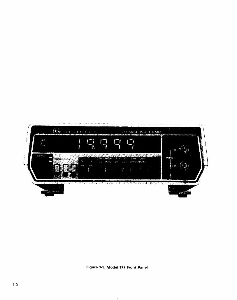
Figure l-l. Model 177 Front Panel
1-o
SECTION 1 GENERAL INFORMATION
1.1 INTRODUCTION
The Keithley Model 177 Microvolt DMM is a versatile, highly sensitive digital multimeter which is used for measurement of DC and AC voltages, DC and AC currents, as well as resistance. For a complete summary of ranges for each of these five functions, refer to the specifications at the front of this manual. Ranges and functions are easily selected with front panel pushbuttons, while connections for all functions are easily made with a single set of front panel input ter- minals.
1.2 MODEL 177 FEATURES
1. 4% Digit LED Display-An easy to read 4% digit display shows 20,000 counts of information with automatic polari- ty indication.
2. l~V/lmQ Resolution-The Model 177 is capable of reading DC voltages es low as 1wV and resistances down to 1mR.
3. Front Panel Zero-The front panel zaro control may be used to compensate for thermal offsets or lead resistance when making measurements.
4. Analog Output-An analog output of lV/lO,OOO counts is available on the rear panel.
1.3 WARRANTY INFORMATION
Warranty information may be found inside the front cover of this manual. Should it become necessary to usa the warran- ty, contact your nearest Keithley representative or the factory to determine the correct course of action. Keithley Instru- ments maintains service facilities in the United States, West Germany, Great Britain, France, the Netherlands, Switzerland and Austria. Information concerning the appli- cation, operation or service of your instrument may be directed to the applications engineer at any of these loca- tions. Check inside the front cover of this manual for ad- dresses.
1.4 MANUAL ADDENDA
Information concerning improvements or changes to the instrument that occur after the printing of this manual will be covered in an addendum sheet packed with the instrument. Be sure to review these changes before attempting to operate or service the instrument.
1.5 SAFETY SYMBOLS AND TERMS
The following safety symbols and terms are used in this manual or may be found on the Model 177.
The symbol A on the instrument indicates that the user should refer to the operating instructions.
The symbol #M on the instrument denotes that a potential of 1OOOV or more may be found present on the terminals. Standard safety practice should be observed when such dangerous voltages are encountered.
The WARNING heading used in this manual explains dangers that could result in personal injury or death if nor handled properly. Be sure to read the WARNING informa- tion carefully before performing the associated procedure.
The CAUTION heading is used in this manual explains hazards that could damage the instrument.
1.6 SAFETY PRECAUTIONS
The following safety precautions should be observed before operating any digital multimeter.
1. This instrument is intended for use by qualified personnel who recognize shock hazards and are familiar with the safetY precautions required to avoid possible injury. Read over the manual carefully before operating this instrument.
2. Exercise extreme caution when a shock hazard is present at the instrument’s input. The American National Standards Institute (ANSI) states that a shock hazard ex- ists when voltage levels greater than 30V rms or 42.4V peak are present. A good safety practice is to expect that hazardous voltage is present in any unknown circuit before measuring.
3. Inspect the test leads for possible wear, cracks or breaks before each use. If any defects are found, replace with test leads that have the same measure of safety as those sup- plied with the instrument.
4. For optimum safety do not touch the test leads of the instrument while power is applied to the circuit under tast. Turn the power off and discharge all capacitors, before connecting or disconnecting the instrument.
5. Do not touch any object which could provide a current path to the common side of the circuit under test or power line (earth) ground. Always make meawrements with dry hands while standing on a dry, insulated surface, which is capable of withstanding the voltage being measured.
6. Exercise extreme precaution when tasting high energy power circuits (AC line or mains, etc.). Refer to the oper- ation section of the manual.
7. Do not exceed the instrument’s maximum allowable input as defined in the specifications and operation section.
1.7 SPECIFICATIONS
Detailed Modal 177 specifications are located at the front of this manual.
l-l
1.8 UNPACKING AND INSPECTION
The Model 177 was carefully inspected, both mechanically and electrically, before shipment. Upon receiving the instru- ment, carefully unpack it from the shipping carton and check for any obvious signs of physical damage that might have oc- curred during shipment. Report any damage to the shipping agent at once. Retain the original packing materials in case reshipment becomes necessary. The following items are in- cluded with every Model 177 shipment.
1. Model 177 Micro\+t DMM 2. Model 177 Instruction Manual 3. Additional accessories as ordered.
1.9 SCOPE OF THE MODEL 177 INSTRUCTION MANUAL
This manual contains information necessary to operate and service both the Model 177 and the optional Model 1788 Sat- tery Pack and is divided into the following sections. 1. Section 2 contains operating information.
2. Information necessary to verify that instrument per- formance is within specified accuracy is located in Section 3.
3. Theory of operation is covered in Section 4. 4. Servicing information, including Model 1788 installation
instructions, may be found in Section 5. 5. Replaceable parts information, component layouts and
schematic diagrams are located in Section 6.
1.10 OPTIONAL ACCESSORIES
1.10.1 Power Options
The Model 177 can be powered by line voltage (105-125V at 50.60Hz or 210.250V at 50-GOHz--standard ranges) or the optional Model 1788 Rechargeable Battery Pack. (Optional line voltage rangas are described in Section 2.1 The Model 1788 is available factory-installed or is field-installable. Instal- lation and operating instructions are given in Section 2.
1.10.2 Cables and Connectors
Model 1881 Clip-On Test Lead Set-This set contains two 1.2m (48 in.1 leads with banana plugs at one end and spring- action clip-on probes at the other end.
Modal 1683 Universal Test Lead Kit-This kit contains two Im (40 in.) test leads and 14 screw-in adapter tips. The tips consist of two alligator tips with boots, four banana plugs, phone tips, two spade lugs and four heavy duty tip plugs which permit connection of theModel 177 to virtually any source within its measurement range.
1.10.3 Probes and Shunts
Modal 1600A High Voltage Probe-The Model 1600A High Voltage Probe extends the measurable DC voltage range up to 40kV. It has a 1OOO:l division ratio, so that a reading of 1V on the DMM corresponds to IkV IlOOOV). The Model 1600A has a basic accuracy of lt25% and an input resistance of IOOOMQ. Model 1651 SO-Ampere Shunt-The Model 1651 50.Ampere Shunt permits current measurements of up to 50A AC or DC. The shunt has a resistance of O.OOlQ * 1%. so that a 50A current will correspond to a reading of 50mV I0.0500v). Modal 1692A RF Probe-The Model 1682A RF Probe per- mits measurement of AC voltages at frequencies of 20kHz to 250MHz. AC to DC transfer accuracy is Id6 at lV, and the input voltage range is 0.25V to 15V rms.
Model 1685 Clamp-On AC Current Probe-The Model 1685 Clamp-On Current Probe permits measurement of AC current by clamping around a single conductor, eliminating the need to interrupt the current path. The Model 1685 has a current conversion ratio of O.lV/A with three ranges (2A. 20A, 200A). Accuracy is +4% at 60Hz If6% at 50Hz).
1.10.4 Carrying Case and Rack Mounts
Modal 1684 Carrying Case-The Model 1684 Carrying Case is a hard vinyl case with a fitted foam insert to help pro- tect the Model 177 from damage. There is also room in the case for the instruction manual and small accessories. Models 1010 and 1017 Rack Mounting Kits-The rack mounting kits permit mounting one 11010) or two (1017) Model 177 DMMs in a 19 inch rack for convenient viewing.
1.10.5 Output Options
Model 1792 Isolated SCD Output-The Model 1792 con- verts displayed reading to an electrically isolated, latched and buffered parallel BCD format. Output data includes sign, overrange and busy. It is compatible with Model 177 serial number 14,500 and above, and can be either factory or field installed. Installation of the 1792 precludes installation of Models 1788 or 1793.
Model 1793 IEEE-488 Output-The Model 1793 converts displayed readings to IEEE-488 bus compatible outputs to permit automatic gathering of measurement data. Output in- cludes 4% digit ASCII data, sign an overrange. It operates in either talk-only or addressable modes. The Model 1793 is compatible with Model 177s serial number 16,500 and above, and can be either factory or field installed. Installation of the 1793 precludes installation of the Model 1788 or 1792.
1-2
SECTION 2 OPERATION
2.1 INTRODUCTION
This section provides information needed for preparation for use and operation of the Model 177 and Model 1788.
2.2 SAFETY PRECAUTIONS FOR HIGH ENERGY CIRCUITS
To optimize safety when measuring voltage in high energy distribution circuits, read and observe the directions in the following warning.
WARNING Dangerous arcs of an explosive nature in a high energy circuit can cause severe personal injury or death. If the mater is con- nected to a high energy circuit when sat to a current range, low resistance range or any other low impedance range, the circuit is virtually shorted. Dangerous arcing can result even when the mater is set to a voltage range if the minimum safety spac- ing is reduced.
When making measurements in high energy circuits use test leads that meet the following requirements: 1. Test leads should be fully insulated.
2. Only use test leads that can be connected to the circuit (e.g. alligator or spade lugs) for a hands-off measurement.
3. Use test leads that do not reduce the arc protection by decreasing the voltage spacing between conductors or terminals.
Use the following sequence when testing power circuits: 1, De-energize the circuit using the regular installed connect-
disconnect device such as the circuit breaker, main switch, etc.
2. Attach the test leads to the circuit under test. Use ap- propriate safety rated leads for this application.
3. Set the DMM to the proper function and range. 4. Energize the circuit using the installed connect-disconnect
device and make measurements without disconnecting the DMM.
5. De-energize the circuit using the installed connect- disconnect device.
6. Disconnect the test leads from the circuit under test.
2.3 PREPARATION FOR USE
The Model 177 is shipped ready-to-use on line power. The instrument may also be powered from rechargeable batteries
(when the optional Model 1788 Rechargeable Battery Set is installed.)
2.4 OPERATION ON LINE POWER
The Model 177 DMM has a three-wire line cord which mates with third-wire grounded receptacles. Connect the insfru- ment to AC line power as follows:
1
CAUTION Connect only to the line voltage selected. Application of incorrect voltage can damage the instrument.
Sat the LINE VOLTAGE switch on the back of the instru- ment to correspond to the line voltage available. Standard ranges are 105V to 125V and 210V to 250V AC as shown in Figure 2-l. Optional ranges of 9OV to 11OV and 18OV to 220V AC are also available as shown in Figure 2-2. As in- dicated on their respective rear panels, the standard line voltage range instruments use an internal line fuse (F102) of 1/8A rating and the optional line voltage range instru- ments use a 3/16A fuse. See Section 5.
WARNING Ground the instrument through a property earth-grounded receptacle before opera- tion. Failure to ground the instrument can result in savera injury or death in the avant of short circuit or malfunction.
2. Plug the power cord into a properly grounded outlat. Operate the Model 177 DMM as described in paragraph 2.7.
2.5 OPERATION ON BATTERY PACK POWER
The Model 177 DMM may also be operated from rechargeable sealed lead-acid batteries contained in the optional Model 1788 Battery Pack. The battery pack will operate the Model 177 DMM for up to six hours. Circuits within the battery pack will automatically shut down the in- strument when the battery charge is insufficient to maintain accurate readings. To install the Modal 1788, refer to Section 5. 2.6 BATTERY CHARGING
The Modal 1788 Battery Pack contains an integral battery charger. To charge the battery pack, install the battew pack in the Model 177 DMM as described above and proceed as follows: 1. Connect the instrument to line power as described in
paragraph 2.4.
2-1
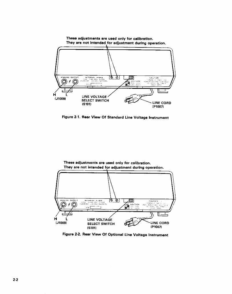
These adjustments are used only for calibration. They are not intended for adjustment during operation.
/
(JlOOS) LINE VOLTAGE SELECT SWITC
IP1007)
Figure 2-1. Rear View Of Standard Line Voltage Instrument
These adjustments are used only for calibration. They we not intended for adjustment during operation.
/+J H ,JlOO,:
LINE VOLTAGL &x SELECT SWITCH (SlOll
-v IP10071
Figure 2-2. Rear View Of Optional Line Voltage Instrument
2-2
2. With the power switch off, the battery charge circuitry is automatically energized to charge the battery et the maxi- mum rate. When the battev pack is first installed, or if it has completely discharged, allow it to charge for at least 14 hours in this condition.
NOTE For maximum battery life, do not allow the bat- tery pack to remain completely discharged. Con- stant charging will not harm either the battery pack or the instrument. The Model 177 may be operated up to six hours from fully charged bat- teries. However, since 10 charge/discharge cycles may be required to reach full batten/ capacity, less than six hours DMM operation can be expected when the battery pack is first in- stalled.
3. When the Model 177 DMM is in use on line power, the bat- tery charger maintains a trickle charge on the battery pack.
2.7 OPERATING INSTRUCTIONS
The basic operating instructions for the Model 177 DMM are outlined in the following steps, and condensed operating in- structions are provided on the bottom cover of the instru- ment and contained in Table 2-l. These instructions should only be used after becoming completely familiar with the operation of the Model 177 through day-to-day use. Until this familiarity has been achieved, best performance and safest operation will be obtained by using the individual instructions provided in this section. Refer to Figure 2-3 and operate the DMM es follows:
1. Turn on the power by depressing the ON/OFF pushbutton and allow a 10 minute warm-up time. Allow additional warm-up for zero stability on lowest DMM and Q ranges.
2. Select the function with the AC/DC, R, V, or A push- buttons.
3. Select the range by depressing the appropriate push- button.
4. Connect the source to the INPUT terminals. Accessories described in Section 1 should be used as required.
CAUTION Do not exceed the maximum input ratings shown below.
DCV
ACV
DCA. ACA
R
QOmV, ZOmV, ZVI: 450V rms continuous; 1200V peak momentan/, for up to eight seconds per minute maximum. (20.12OOV): 12OOV peak. ;I ;;;ges): 1OOOV rms; 1400V peak;
. (All Ranges): ZA, 250V DC or rms (fuse pro- tected). (All Ranges): 350V peak.
2.9 ZERO ADJUSTMENT
The front panel zero adjustment provides compensation for test lead resistance and thermal EMFs generated in the cir- cuits connected to the DMM input terminals. The zero adjusr- ment is operative on the 20mV and 200mV ranges of DCV. 20 and 200R ranges and all DCA ranges. In general, the zero must be readjusted whenever the function is changed and the measurement is to be made on a range where the zero adjusts ment is operative. The accuracy specifications assume that zero is adjusted on the lowest range of the function. Where applicable, a specific zero adjustment instruction is provided in the description of how to make the particular function measurement.
2.9 DC VOLTAGE MEASUREMENT
The Model 177 measures DC voltages from l,lV/digit to 12OOV. The maximum displayed reading is 19999. Overrange is indicated by a flashing 0000 except on the 12COV range. On the 1200V range, the display can read beyond the maximum allowable input voltage. Use the Model 177 to measure DC volts as follows:
CAUTION Do not exceed the maximum input voltage ratings, or instrument damage may occur.
1. Turn on power with ON/OFF pushbunon and select DC with the AC/DC pushbutton.
2. Select the desired range from the six ranges available. The decimal point is positioned by the range pushbuttons. The 1200V DC range is selected by the 1000 pushbutton.
NOTE The 20M pushbutton is inoperative for DC volts. If this pushbutton is inadvertantly depressed. the Model 177 will read zero regardless of the voltage applied and the eight second per minute overload rating will apply.
3. Connect the signal to be measured between the INPUT HI and LO binding posts. The binding posts accept wires, spade lugs or banana plugs for ease of connecting the cir- cuit to be measured. Low thermal cabling and connections are recommended for measurements on the 20mV and 200mV ranges.
4. For the top four ranges. merely observe the displayed digits, polarity sign and decimal point locations. The top four ranges are direct-reading in volts. Nominal settling time is located to within one digit of final reading.
5. For the 20mV and 200mV ranges, the front panel ZERO must be adjusted to obtain rated accuracy. This adjust- ment is necessary to compensate for thermal EMFs generated by the connections to the circuit to be measured. These voltages may be only a few microvolts or several tens of microvolts. The zero adjustment span is set up at the factory to allow at least f75,tV adjustment. To adjust zero, proceed as follows:
2-3
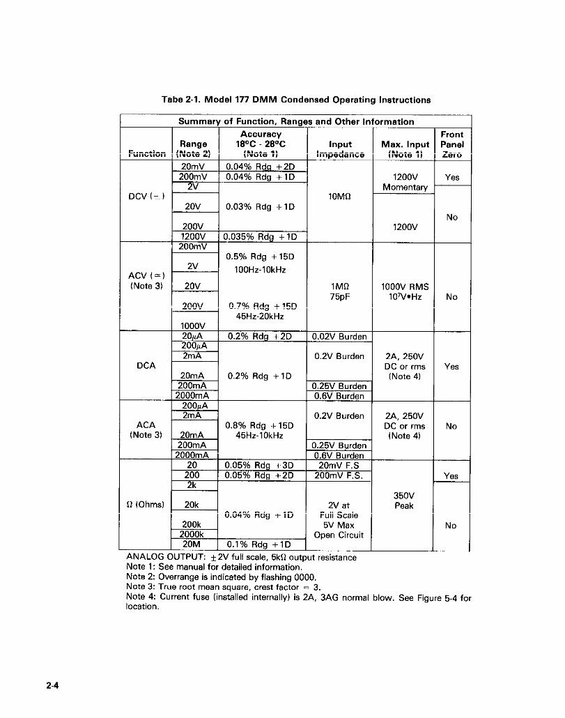
Taba 2-1. Model 177 DMM Condensed Operating Instructions
Summary of Function, Ranges and Other lr
0.03% Rdg + 1 D
0.5% Rdg +15D
lOOHz-10kHz
0.7% Rdg + 15D
0.2V Burden
0.8% Rdg +15D
ANALOG OUTPUT: f2V full scale. 5k0 outout resistance Note 1: See manual fir detailed infbrmation.’ Note 2: Overrange is indicated by flashing 0000. Note 3: True root mean square, crest factor = 3. Note 4: Current fuse (installed internally) is 2A. 3AG normal blow. See Figure 5-4 for location.
lrmation
Max. Input (Note 1)
1200v Momentary
1OOOV RMS 10WHz
2A. 250V DC or rms (Note 4)
2A. 250V DC or rms
(Note 4)
350v Peak
Front Panel Zero
Yk?S
1
No
No
YC?S
No
No
2-4
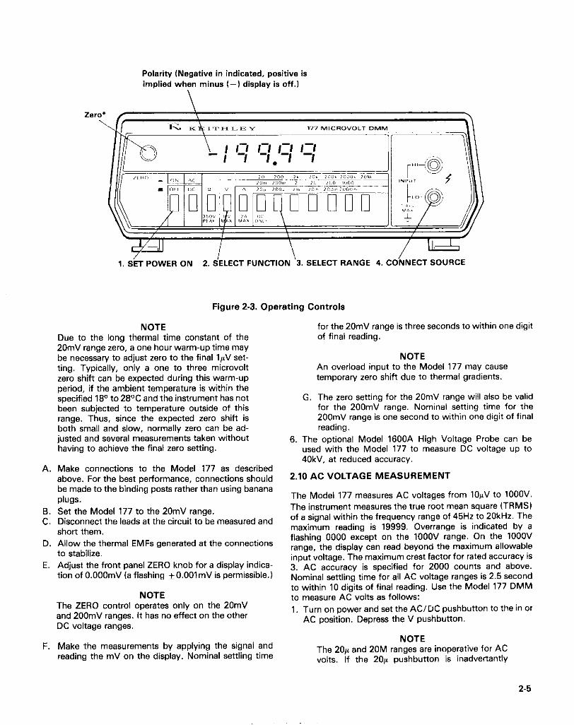
Polarity (Negative in indicated, positive is implied when minus I-1 display is off.1
A.
Z:
D.
E.
F.
1. SET POWER ON 2. SELECT FUNCTION ‘3. SELECT RANGE 4. CONNECT SOURCE
Figure 2-3. Operating Controls
NOTE Due to the long thermal time constant of the 20mV range zero, a one hour warm-up time may be necessary to adjust zero to the final l@ set- ting. Typically, only a one to three microvolt zero shift can be expected during this warm-up period, if the ambient temperature is within the specified lfl” to 28% and the instrument has not been subjected to temperature outside of this range. Thus, since the expected zero shift is both small and slow, normally zero can be ad- justed and several measurements taken without having to achieve the final zero setting.
Make connections to the Model 177 as described above. For the best performance, connections should be made to the binding posts rather than using banana plugs. Set the Model 177 to the 20mV range. Disconnect the leads at the circuit to be measured and short them. Allow the thermal EMFs generated et the connections to stabilize. Adjust the front panel ZERO knob for a display indica- tion of O.OOOmV (a flashing fO.OOlmV is permissible.)
NOTE The ZERO control operates only on the 20mV and 200mV ranges. It has no effect on the other DC voltage ran&.
Make the measurements by applying the signal and reading the mV on the display. Nominal settling time
G.
for the 20mV range is three seconds to within one digit of final reading.
NOTE An overload input to the Model 177 may cause temporary zero shift due to thermal gradients.
The zero setting for the 20mV range will also be valid for the 200mV range. Nominal setting time for the 200mV range is one second to within one digit of final reading.
6. The optional Model 1600A High Voltage Probe can be used with the Model 177 to measure DC voltage up to 40kV. at reduced accuracy.
2.10 AC VOLTAGE MEASUREMENT
The Model 177 measures AC voltages from 1OrV to 1OOOV. The instrument measures the true root mean square (TRMSI of a signal within the frequency range of 45Hz to 20kHz. The maximum reading is 19999. Overrange is indicated by a flashing 0000 except on the 1OOOV range. On the 1OOOV range, the display can read beyond the maximum allowable input voltage. The maximum crest factor for rated accuracy is 3. AC accuracy is specified for 2000 counts and above. Nominal settling time for all AC voltage ranges is 2.5 second to within 10 digits of final reading. Use the Model 177 DMM to measure AC volts as follows:
1. Turn on power and set the AC/DC pushbutton to the in or AC position. Depress the V pushbutton.
NOTE The 20~ and 20M ranges are inoperative for AC volts. If the 20~ pushbutton is inadvenantly
2-5
depressed, the display will read overrange, signalling the user to go to the next higher range. If 20M is depressed, the display will read zero regardless of the voltage applied. The method of calibrating the converter may yield an offset up to 125 digits with the Model 177 input shorted. This does not affect instrument ac- curacy.
2. Select the desired range from the five ranges available.
CAUTION MAXIMUM ALLOWABLE INPUTVOLTAGE (All ranges): IOOOV rme, 1400V peak. 107V*Hz maximum. Do not exceed the max- imum rating. Instrument damage may oc- cur.
3. Connect signal to be measured between INPUT HI and LO terminals. Observe the displayed digits and decimal point location. The 200mV range is direct-reading in mV and the remaining four ACV ranges are direct-reading in volts.
4. The crest factor (CFI is the ratio of the peak voltage to the rms voltage as follows:
CFrVPEAK
VRMS
NOTE There will be some additional measurement error for signals with a crest factor greater than 3 fCF>3l.
Typical crest factors are as follows:
Sine Wave Square Wave rriangular Wave Positive pulse train (duty cycle CF = 3 is 0.11)
CF = 1.4 CF = 1 CF = 1.7 CF = \/l/duty cycle
5. The optional Model 1682A RF Probe can be used with the Model 177 to measure 0.25V to 15V rrn.s AC signals with a frequency of 2OkHz to 250MHz (and above at reduced ac- curacy).
6. Refer to paragraph 2.14 for TRMS measurements of a signal with both AC and DC components.
2.11 RESISTANCE KZ, MEASUREMENT
The Model 177 DMM measures resistance from lmD/digit to 20MD. See Table 2-2 for ranges. Nominal settling times to within one digit of final reading are: three seconds on the 200 range; two seconds on the 2000kD and 20MD ranges; one se- cond on the other four g ranges. Use the Model 177 to measure resistance as follows: 1. Turn on power and depress the R pushbutton.
2-6
CAUTION MAXIMUM ALLOWABLE INPUTVOLTAGE (All ranaesl: 350V oeak. Do not exceed maximum rating. l&trument damage may occur.
2. Connect the circuit to be measured to the INPUT binding posts and select the desired range from the seven available.
?iii%gzm x; il binding post treol IS negatrve.
Range Maximum Setting Reading
200* 19.999 2ooll* 199.99
2kD 1.9999 20kD 19.999
200kD
I
199.99 2000kR 1999.9 20MD 19.999
*Front Panel Zero
Table 2-2. Resistance Ranges
Full Scale Voltage**
20mV 200mV
2v 2v 2v 2v 2v
All Ranges
Nominal Applied Current
1mA 1mA 1mA
1OOfiA 1 Oj.cA ld
O.lfiA
3. Observe the displayed digits and decimal point to measure resistance using the 2k, 20k. 200k. 2000k and 20MR ranges. The full scale voltage drop for these ranges is 2V which is sufficient to cause forward conduction of semiconductor junctions. The HI (Red) terminal is negative. To measure a resistance in parallel with a semiconductor junction without turning on the junction, either reverse bias the junction or select the next higher D range. The latter method is possible because of the one decade reduction of applied test current, but will result in a measurement with 3% digit accuracy. It is suggested that the 2kg range be used for diode testing. This range has a nominal 1mA test current and the displayed reading is the forward voltage drop in volts.
NOTE The front panel ZERO control operates only on the 200 end 2OOD ranges. It has no effect on the other resistance ranges.
4. Before making measurements on the 2051 or 200R ranges, adjust front panel ZERO on the 20R range to compensate for test lead resistance. Best performance will be obtained on the low ohm ranges when test connections are made to the binding posts, rather than using banana plugs. Adjust ZERO and make resistance measurements as follows:
A. Select 200 range. D. Adjust front panel ZERO knob for a display indication of
B. Disconnect the test leads at the circuit to be measured O.OOO,rA * ,001 flashing.
and short them. If measurement is to be made right at 2. After adjusting ZERO, use the Model 177 to measure DC the INPUT terminals (no test leads used) place a short, current as follows: such as a piece of copper wire, across the binding posts. CAUTIONS
C. Adjust the front panel ZERO knob for a display indica- Do not install e larger capacity fuse then tion of 0.000 *O.OOlG (flashing). The nominal ZERO the one originally supplied L?Al. Current adjustment span is 200mD. fuse FlOl (shown in Figure 5-4) protects the
instrument against over-current. NOTE
The specified accuracy for the 2OD and 2OOG A. Select the desired range from the six ranges available.
ranges assumes that ZERO was adiusted on the 8. Connect the circuit to be measured to the INPUT ter-
20irange. Re-adjust zero on the 2dg range each time that a different set of leads is used or whenever measurements have been made on
minals. C. Read the displayed polarity, digits and decimal point.
Select the next higher range if overrange is indicated.
either the two lowest DC voltage ranges or any DC current range. The zero setting for those measurements will be different than the zero set- ting of ohms, Also, re-adjust zero whenever the instrument is used outside the temperature range of 18O to 28OC.
D. Reconnect the test leads to the circuit to be measured. E. Select either 2OD range or 2000 range. Read the
displayed digits and decimal point.
NOTE An input overload to the Model 177 may cause a temporary zero shift due to thermal gradients.
2.12 DC CURRENT MEASUREMENT
2.13 AC CURRENT MEASUREMENT
The Model 177 measures AC current from 1OnAldigit to 2A. over five ranges. (The’ 20r~A and 20M ranges are not operative. See note below.1 The 200r~A range is direct- reading in microamperes. The remaining AC current ranges are direct-reading in milliamperes. The maximum reading is 19999. Overrange is indicated by a flashing 0000. Overload is protected by fuse FlOl, a 2A, 3AG normal-blow fuse. The instrument measures the true root mean square ITRMSj of waveforms in the frequency range of 45 to 10kHz. Use the Model 177 to measure AC current as follows: 1. Turn on power and set the AC/DC pushbunons to in or
AC position. Depress the A pushbunon.
CAUTION The Model 177 measures DC current from lnA/digit to 2A. over six ranges (the 20M range is not operative and the
Do not install a larger capacity fuse then
instrument will read zero if 20M pushbutton is depressed). the one supplied. Current fuse FlM (shown
The maximum reading is 19999. Overrange is indicated by a in Figure 5-41 protects the instrument
flashing 0000. Overload is protected by fuse FlOl, a 2A 3AG against over current.
normal-blow fuse. Nominal settling time for DC current 2. Connect the circuit to be measured to the INPUT terminals ranges is one second to within one digit of final reading ex- and select the desired range from the five ranges available. cept three seconds on 20pA range.,
NOTE 1. Before making DC current measurements, the front panel
ZERO must be adjusted on the 20@ range. This adjust- The 20/1A and 20M ranges are not operative for AC current measurements. If the 20uA push-
ment is necessary to remove any offset that was intr- button is inadvertently depressed, an overrange oduced by adjusting ZERO for a low DC voltage measure- mentor a low g measurement. This adjustment will also be
will be indicated, signalling the user to go to the
necessary whenever the instrument is used outside of the next higher range. If the 20M pushbutton is de-
temperature range of 18O to 28Y. The specified accuracy pressed, the instrument will read zero.
for the DC current ranges assumes that ZERO was ad- 3. Read the displayed digits and decimal point. justed on the 2OpA range. Adjust ZERO as follows: A. Disconnect all circuits from the Model 177 INPUT ter- NOTE
minals. The INPUT terminals must have an open cir- AC accuracy is specified for 2000 counts and cuit~ above. The method of calibratina the converter _-...
8. Turn on power and set the AC/DC pushbunon to the out or DC position.
C. Depress A and 20~ pushbuttons.
may yield an offset up to 80 digits with the Model 177 input shorted. This does not affect in- strument accuracy. There will be some addi- tional measurement error for signals with a crest
2-7
factor greater than 3 (CF>31.Refer to paragraph 2.10 for information on how to determine the crest factor of a waveform.
4. Refer to paragraph 2.14 for TRMS measurements of a signal with both AC and DC current components:
2.14 TRMS MEASUREMENTS (AC + DC)
The Model 177 measures the AC component of a waveform and does not measure the DC component. Use the Model 177 to measure TRMS of a signal which has both AC and DC components as follows:
1. Measure and record the AC and DC components separate- lV. A. Refer to paragraph 2.9 for DC voltage measurement. 6. Refer to paragraph 2.10 for AC voltage measurement. C. Refer to paragraph 2.12 for DC current measurement. D. Refer to paragraph 2.13 for AC current measurement.
2. Compute the TRMS value using the following equation:
ETRMS =“EDc~ + EACH OR lTRMS =‘IDC2 + lAC2
2.15 ANALOG OUTPUT
The rear panel accessible ANALOG OUTPUT provides a f2V full scale DC signal IlOk counts = 1V). The ANALOG OUTPUT is operable for all instrument ranges and functions. The output polarity of the analog voltage is negative for the
ohms (0) function, positive for AC function and non-inverting for DC functions. The effective analog output resistance is 5kR (4kn in series with the HI output to protect the Model 177 against externally applied voltage and 1 k0 between input LO and analog output LO to prevent a ground loop when con- nection is made to a grounded load, oscilloscope or recorder). The analog output voltage is compatible with most modern analog recorders and may be used to determine signal changes with respect to time or other variables. With respect to the signal input and analog output, the Model 177 acts as an amplifier (for mV signals), an attenuator (for kV signals) or a converter to DC volts (for AC current or resistance signals). Output accuracy is the same as the display except on ohms; up to *0.05% error can be ex- pected due to the ratio-metric method used. The analog out- put floats at input LO. For this reason, do not connect a voltage source across INPUT LO and ANALOG LO. This will result in a measurement error and may damage the Model 177 if the voltage is greater than 15V. When the instrument is in an overrange condition, up to + 15V DC may be at the ANALOG OUTPUT dependent upon the function, range and level of the input signal.
2.16 TILT SAIL ADJUSTMENT
The tilt bail of the Model 177 may be used to elevate the in- strument to a convenient viewing height. To adjust the bail, pull the bail out from each side of the case and rotate it to the desired position. Release the bail to allow it to lock into posi- tion.
2-6
SECTION 3 PERFORMANCE VERIFICATION
3.1 INTRODUCTION point, perform a complete calibration as described in Section 5, unless the instrument is still under warranty.
Performance verification may be performed upon receipt of NOTE the instrument to ensure that no damage or misadjustment has occurred during transit. Verification may also be par-
Performance verification should be performed
formed whenever ther is question of the instrument’s ac- by qualified personnel using accurate and
curacy, and following calibration, if desired. reliable test equipment.
3.4.1 Initial Conditions NOTE
For instruments that are still under warranty (less than 12 months Since date of shipment), if the
Before beginning the verification procedure the instrument
instrument’s performance falls outside specifica- must meet the following conditions:
tions at any point, contact your Keithley 1. If the instrument has been subjected to extremes of
representative or the factory immediately. temperature, allow internal temperatures to stabilize for one hour minimum at the environmental conditions
3.2 RECOMMENDED TEST EQUIPMENT specififed in paragraph 3.3
2. Turn on the Model I77 and allow it to warm up for one
Recommended test equipment for performance verification is hour. The instrument may be operated from either line
listed in Table 3-1. Alternate test equipment may be used. power or from battery pack power, as long as the battety
However, if the accuracy of the alternate test equipment is pack has been fully charged as described in paragraph 2.6.
not at least IO times better than the instrument’s specifica- tions, additional allowance must be made in the readings ob- WARNING
tained. Some of the equipment listed in Table 3-I is not 10 Some procedures require the usa of high
times batter than the Model I77 specifications because such voltage. Take care to prevent contact with
equipment is not readily available. In these instances, the live circuits which could causa electrical
verification procedures indicate the equipment shock resulting in injury or death.
manufacturer’s specified uncertainty, and include the uncsr- tainty in determining the allowable reading for the Model 177. 3.4.2 DC Voltage Accuracy Check (2V to 1200V Ranges)
3.3 ENVIRONMENTAL CONDITIONS I. Select DC voltage function with the AC/DC V push- buttons.
All measurements should be made at an ambient temperature 2. Connect the DC calibrator to the instrument.
within the range of 18” to 28OC (65” to 62OFl. and a relative 3. Select the 2V range. and apply positive 2VDC to the humidity of less than 80%. DMM. The reading must be within the limits specified in
Table 3-2. 3.4 PERFORMANCE VERIFICATION PROCEDURE 4. Select each remaining range and apply required voltage
specified in Table 3-2. Verify that the reading is within Use the following procedures to verify the basic accuracy of specifications. the Model 177 DMM for voltage, resistance and current measursments. If the instrument is out of specification at any
5. Repeat all checks with negative voltage.
Table 3.1. Recommended Test Equipment For Perfomance Verification
Description DC Calibrator
AC Calibrator AC Amplifier Decade Resistor
current source
1OOn Per Step 4-Terminal Low Thermal Resistor
*0.002% or 2O@V O.lV, 1v. IOV, IOOV 10.01% 1ooov @ 0.04% 1900, 1.9kQ. 19kQ. 190kn. 1.9MQ. IOMn, iO.OI% 100rA. lmA, lOmA, IOOmA, 1A
10:1 divider within 50 PPM
Mfr. Fluke
Fluke Fluke ESI
Fluke
ESI
3-l
Table 3-2. DC Voltage Performance Check (2V to 1200V Rangel
3.4.3 DC Voltage Accuracy Check (20mV and 200mV Rangesl
1. Select DCV and 20mV range. 2. Disconnect test leads at the DC calibrator and short
them. Adjust Model 177 front panel ZERO for a display indication of O.OOOmV *O.OOlmV flashina.
3. Connect the DC calibrator and select 200mV range.
4. Set the DC calibrator to an output of +O.l9OOOOV.
5. Verify that the Model 177 reading is between + 189.89 to + 190.11mV. Note that the allowable reading includes a i2 digit allowance for the uncertainty of the DC calibrator.
Table 3-3. AC Voltage Accuracy Check
Range Applied Voltage @lkHz lOO.OOmV 1 .oooov 1o.ooov 1oo.oov 1ooo.ov @45Hz 1o.ooov @2OkHz 1o.ooov
Allowable Readings at 180 to 28Y.z
6. Repeat steps 4 and 5 with negative voltage.
7. Select 20mV M”Qc?. 8. Connect the DC calibrator, low thermal resistor and
Model 177 as shown in Figure 3-1.
9. Temporarily disconnect the leads from the DC calibrator and short them. Adjust Model 177 front panel ZERO for a display indication of 0.000 * O.OOlmV flashing.
10. Set the DC calibrator to an output of +O.l9OOOOV.
200mV 2v
2ov 2oov
1ooov
99.35 to 100.65mV 0.9935 to 1.0065V 9.935 to 10.065V 99.35 to 100.65V 993.5 to 1006.5V
2ov
2ov
9.915 to 10.085V
9.915 to 10.085V
11. Verify that the Model 177 readin is between + 18.987 3.4.5 Resistance KU Accuracy Check ~~^^_^ .,~
3. Set the DMM to the 200mV range and apply 1OOmV AC to the DMM. The reading must be within the limits specified in Table 3-3.
4. Select the 2,20 and 200mV ranges and apply the required voltages as specified in Table 3-3. Verify that the readings are within spcifications.
5. To check 1OOOV range, connect the AC calibrator amplifier to the output of the AC calibrator per the manufacturer’s instructions. Connect the amplifier output to the Model 177 INPUT terminals. Set the AC calibrator for amplifier output of lOOO.OOOV at 1kHz. Verify that the DMM reading is within the specified limits in Table 3-3.
6. To check accuracy at 45kHz and 20kHz. select the 20V range. Apply the voltage specified in Table 3-3 at 45Hr. then repeat at 20kHz. Verify that the DMM readings are within the specified limits.
1 I
ancl + IY.VIXnV. Note, that, the allowable reading in- cludes *2 digits for DC calibrator uncertainty and * 1 1. Select resistance function by depressing n pushbuttons.
digit for low thermal resistor uncertainty. 2. Select 2000 range.
12. Repeat steps 10 and 11 with negative voltage. 3. Connect the decade resistor to the DMM. 4. Set the decade resistor to zero and compensate for lead
resistance by adjusting front panel ZERO for a display in- THERMAL dication 00.10 f .OlQ flashing. R6SlSTOR 5. Set the decade resistor to 190% Verify that the reading for
the 200R range is within the limits specified in Table 3.4. 6. Select the 2k0 ra”Qe.
7. Set the decade resistor to zero and measure the resistance of the test leads. Subtract this reading from the displayed reading in all of the following steps.
Figure 3-I. Test Circuit For 20mV DC Accuracy Check 8. Set the decade resistor to 1.900kfI. Verify that the reading is within the limits specified in Table 3-4.
9. Continue by selecting the next range and measure the next 3.4.4 AC Voltage Accuracy Check resistance as specified in Table 3-4. Test each item in the
1. Select AC voltage function with the AC/DC and V table and verify that each reading is within specifications.
pushbuttons. 2. Connect the AC calibrator to the DMM. Set the calibrator
frequency to 1 kHz.
3-2
Table 3-4. Resistance Accuracy Check
Allowable Reading at Range Resigtance 180 to 28% l
2000 1900 189.86 to 190.140 * 2 diQits 2kQ 1.900kR 1.8989 to 1.9011 kO + 2 disits
20kR 19.000kfl 18.989 to 19.011kR + 2 digits 200kR 190.00kfI 189.89 to 190.11kfI +2 digits
2000kO 1900.0k0 1898.9 to 1901.lkR *2 digits 20MR lO.OOOMfl 9.988 to 10.012MR f 1 digit
*Manufacturer’s specified unceflainty of the decade resistor in digits. This uncertainty has been added to the specified accuracy of the Model 177 to obtain the allowable reading.
3.4.6 DC Current Accuracy Check
1. Select the DC current function with the AC/DC and A pushbuttons.
2. Select the 20cA range. With an open circuit at the INPUT terminals of the Model 177, adjust the front panel ZERO for a display indication of 0.000 1tO.00l~A flashing.
3. Connect the DC current source to the DMM.
4. Select each range and apply the required current as specified in Table 3-5. Verify that each reading is within specification.
Table 3-5. DC Current Accuracy Check
Applied - Current
lOO.OO~A --
L 1 .OOOOmA lO.OOOmA lOO.OOmA lOOO.OmA
I 0.9979 to 1.002imA 9.979 to 10.021mA 99.79 to 100.21mA 997.9 to 1002.lmA
3.4.7 Analysis
If the instrument is out of specified limits at any point in Table 3-2 through 3-5, calibrate the DMM as described in Section 5. If the unit is still under warranty, refer to the ncate in paraQraph 3.1.
NOTE It is not necessary to specifically check the 20R or 20uA ranaes. or a”” of the ACA ranaes. The circuit components that determine th& accu- racy have been checked elsewhere in the verification procedure.
3-313-4

SECTION 4 THEORY OF OPERATION
4.1 INTRODUCTION 4.2.1 Signal Conditioning
This section contains circuit descriptions for the Model 177 DMM and the optional Model 1788 Battery Pack. An overall block diagram of signal flow is provided in Figure 4-l. The schematic diagrams are contained in Section 6 of this manual. The Model 177 schematic is drawing number 29658E and schematic drawing number 29659C is for the Model 1788.
Signal conditioning icludes: DC attenuation (on the 20, 200 and 1200V ranges), modulation and demodulation of the DC signal by the chopper buffer/amplifier with Xl00 and X10 gain Ion the 20 and 200mV ranges, respectively), AC atten- uation (on the 20, 200 and 1OOOV ranges), AC amplification (on the 200mV and 20V ranges), AC-to-DC conversion, ohms source and conversion, and current shunts as shown in Figure 4-l. 1. In the DCV mode, signal conditioning to the A/D converter
consists of range and function switching, range resistors (attenuator) and the chopper buffer/amplifier. For all ranges, the DC input signal is attenuated/amplified to pro- vide a *2V full scale output to the AID converter. In the DCA mode, the voltage developed across the shunt resistor is applied directly to the input of the chopper amplifier. A chopper gain of Xl0 is used for all ranges ex- cept 20A which uses X100.
4.2 OVERALL OPERATION
The Model 177 w?s a 2V (20,000 count) full scaleanalog-to- digital (A/D) converter with a 4% digit multiplexed display. Signal conditioning permits the AID converter to ac- comodate full scale DC voltage and current measurements over seven ranges.
0 SENSE
OPTIONAL SAlTERY
AC AMPLIFIER/ TRMS AC CONVERTER
-4x=
R CURRENT OUTPUT
DC INPUT
il;- DC AlTEN”ATOR/R 0 SOURCE RESISTORS FUNCTION e RANGE ii SWITCHING
AC
CHOPPER FEEDBACK I BUFFER/
AMPLIFIER *ZVFS OUT
A
I
DIGITAL OUTPUT c---7 L---J DISPLAY
L
% REFERENCE
PACK r-----7 I MODEL ’ I 1788 I L-----A
t
t 390Hz CHOPPER DRIVE
0 FRONT PANEL ZERO
IWkHz CLOCK
I OSClLLATOR
Et DIVIDER
Figure 4-1. Model 177 Simplified Signal Flow Block Diagram
4-1
2. In the ACV mode, AC inputs for all ranges pass through the AC converter which consists of an amplifier/attenuator and a TRMS converter, as shown in Figure 4-2. The AC in- put is scaled by the amplifier/attenuator to 2V rms full scale for all ranges. The TRMS converter provides a positive DC output signal which is proportional to the true root mean square AC signal. This DC signal is the input to the A/D converter. In the ACA mode, the shunt voltage is applied to the input of the AC converter. The amplifier/at- tenuator provides a x 10 gain for all AC current ranges.
3. Ohms conversion-Resistance measurements ara made by supplying a constant current from the ohms converter to the unknown resistor (Rx). The resulting voltage developed across the unknown resistor is proportional to its resistance, and this voltage is applied to the input of the chopper amplifier used for DC volts. The chopper amplifier output to the A/D converter is scaled to -2V full scale for all ohms ranges. Scaling of the ohms signal over the seven ranges is accomplished by using five constant current levels and the three gains of the chopper amplifier.
4.2.2 AID Converter
The A/D converter is a large scale integration (LSI) ratiometric device. Converter output is a multiplexed five digit number, in binary coded decimal IBCD) form which is equal to the ratio of the input voltage to the reference voltage. A separate clock circuit supplies a 1OOkHz timing input to the in- tegrated circuit, which also multiplexes the BCD output. The full scale AID input for all ranges of the Model 177 is 2VDC. with the polarity determined by the function as follows: ACV and ACA. +2V; DCV and DCA. rt2V; Resistance (0). -2V.
4.2.3 Range Switching
It is important to note that the range switches on schematic 29658E are identified by the front panel marking for the L2 ranges. The corresponding V and A ranges may either be determined from the instrument front panel or by using Table 4-l.
4.3 AC CONVERTER
When making AC voltage measurements, the AC converter scales the input signal by appropriate attenuation or amplification, performs TRMS conversion and provides the equivalent positive DC level to the A/D for display. Input resistance for AC volts is 1MD IR107). Shunt capacitance is less than 75pF. Signal conditioning is as follows:
4.3.1 Scaling
Scaling is performed in the first two stages, as shown on schematic drawing number 29658E and summarized in Table 42. Scaling is performed by using a relay and FET switches to switch feedback resistors in the attenuator IUlOl) and the amplifier (U102). The actual gains used in attenuator UlOl are 0.99, 0.0099 and 0.00099. Amplifier U102 gains are nominally 1.003 and 10.03. The combined gain of UlOl and U102 is offset low to permit gain adjustment in the TRMS stage. The only adjustments provided in the attenuator and amplifier stages are two high frequency compensation capacitors (Cl02 and C103). AC coupling is used at the input and output of the attenuator and amplifier stages. Input overload protection is provided by diodes (CRlOGand CR1071 and resistors R107 (1MQ. 2WI.
4.3.2 AC Conversion
AC-to-DC conversion is performed b a monolithic TRMS module lU103). Output V, output filtering are done be ore the internal output buffer to
F =&. Averaging and
give a low impedance for the analog output. Potentiometer R113 provides midband (10K count) gain adjustment and R114 establishes output zero (1K count). Capacitor Cl08 is used in the averaging circuit, and Cl09 provides filtering as described above.
4.3.3 AC Current Measurements
For AC current measurements, the appropriate shunt resistor is placed in front of the AC converter. The 200mV range gain configuration is used for all current ranges.
4.4 DC SIGNAL CONDITIONING
For DC voltage measurements, the input resistance is lOMO, which is established by all of the range resistors being con- nected in series to signal ground. On low voltage ranges, the DC input is applied to the top of the resistive divider (range resistor) and to the buffer amplifier input without attenuation. Also, the chopper amplifier has appropriate gain to provide a f2V full scale output to the A/D. On high voltage ranges,
the DC signals are scaled down to *2V full scale by the resistive divider and the chopper is used in the unity-gain Ifollower) mode as a buffer. A summary of input attenuation and chopper amplifier gain is given in Table 4-3.
Table 4-l. Range Switch Correlation
Function Ranges 0 20 200 2k 20k 200k 2000k 20M V 20mX 200m 2 20 200 1000** A 20/L* 2oofl 2m 20m 200m 2000m
*DC Only l *ACV 1000, DCV 1200
4-2
Table 4-2. Converter Attenuation and Amplification AC CONVERTER
Table
**x100 = a101 On **x 1000 = KlOl On
4-3. DC Signal Conditioning Attenuation Gain
Range 20mV
200mV 2v
2ov 2oov
1200v
Input Attenuation
-
+ 10 t 100
i 1000 t
Chopper Gain x 100 x 10 Xl Xl Xl Xl
1
and
4.4.1 Input Attenuation
On the 20, 200 and 1200V ranges, the input signal is atten- uated by the resistive divider to divide by 10, 100 and 1000, respectively. Depressing one of the above range push- buttons, interrupts the unattenuated signal from the volts switch pin 17 and connects the wiper of the appropriate range potentiometer to the input of the chopper. Division by 10, 100 and 1000 is accomplished by connecting the wiper of R155, R156 or R157, respectively.
4.4.2 Chopper
The input signal to the chopper is filtered and applied to a modulator circuit. The AC signal is then amplified and demodulated. A final high gain DC amplifier provides a DC signal to the AID converter and the analog output. 1. Modular Circuit-This circuit converts the input DC signal
to an AC signal with a fundamental frequency component of approximately 390Hz. This frequency was chosen because it reduces the amplitude of higher harmonics of the 50Hz and 60Hz line frequencies, which minimizes beating. The circuit utilizes a dual MOSFET (Q104A and 010413) connected in a series-shunt configuration to main- tain the required high input impedance.
2. AC Amplifier-The AC amplifier uses a JFET-input opera- tional amplifier (U108). The amplifier feedback network provides a gain of approximately 133 at the modulating fre- quency of 390Hz. while maintaining a gain of one for amplifier (U108) DC offset voltages.
6
OHMS CONVERTER
Figure 4-2. Simplified Signal Conditioning
3. Demodulator Circuit-The demodulator is sychronized with the input modulator. A JFET (01051 with low on- resistance is used to alternately attenuate and pass the signal present at the output of AC amplifier U108. This produces a “half-wave rectified” DC signal at the input of the integrator stage, that is inverted with respect to the chopper input signal.
4. DC Amplifier-Amplifier lU109) is connected as an in- tegrator with an offset adjustment. U109 provides suff- cient gain to bring the total open-loop DC gain to about one million. U109 drives the feedback divider network and the A/D converter, and provides the low output im- pedance necessary to drive the analog output. Feedback capacitor (Cl381 was selected to provide nominal settling time, while meeting NMR requirements. When the chop- per is operating as a unity-gain follower, the DC signal prey sent at the output of U109 is the chopper feedback. This is the condition for the 2VDC range and above. On the 200mV and 20mV ranges, where chopper gains of 10 and 100 are required, the resistive divider feeds back a portion of the output of U109 to provide the required gain.
5. Modulator-Demodulator Drive Circuit-CMOS inverters lUlllA and UlllF) provide opposite phase 0 to -15V square waves used to drive MOSFET modulator transistors Q104A and Q1048. lnverter UlllF also drives the
4-3
demodulator JFET Q105. Resistors R118, R119 and R142 and capacitors Cl31 and Cl32 affect the rise and fall times of drive signals. R142 adjusts the rise and fall time of the drive signal to Q104A only, so that the total charge, both positive and negative, transfered to the input can be minimized. The frequency of the drive signal is determined by the clock circuit. Circuitry in UllO divides down a nominal clock frequency of 100kHz to produce 390Hz.
6. Adjustments and Input Protection-The front panel zero control CR2031 permits adjustment of the chopper feed- back to compensate for input thermal EMFs. It functions only on ranges where chopper gain is greater than one. A span of f75V is considered adequate; however, it is typical for R203 to provide a greater than 400V change as it is turned end-to-end. The span is skewed by R128 to give best resolution in both DCV and n. Potentiometer R146 provides a calibration adjustment to compensate 200mV range (X10 gain configuration) and R147 adjusts the Xl00 gain used on the 20mV range. Chopper input resistor R143 limits the input current during momentan/ in- put overloads to 12mA. which is then absorbed by the chopper load resistance (R145 and/or R149) or the power supplies through CR116 and CR117.
7. DC Current Measurements-As previously described, DC current measurements are made by placing the ap- propriate buffer/amplifier shunt resistor on the chopper in- put. A chopper gain of X10 is used for all current ranges except 20A. which uses X100. The front panel zero control (R203) is functional for all DC current ranges.
4.5 OHMS CONVERSION
The ohms converter contains two sections: a floating current source and a high input impedance buffer/amplifier. The chopper employed as a buffer/amplifier in DCV is also used as the high impedance buffer/amplifier for n. Refer to paragraph 4.4 for addition1 chopper theory.
4.5.1 Floatig Current Source
The floating current source involves a differential amplifier W107) driven by the AID reference voltage and the chopper feedback voltage. This results in a constant voltage across the source resistance I = -V reference) which results in a con- stant current in the unknown resistance. One or more range resistors are always connected as the ohms source resistor IRS) when ohms function is selected. Five different constant current levels are supplied by changing the value of R, with the range pushbuttons. These levels are given in Table 4-4. For n, INPUT HI terminal is negative with respect to INPUT LO.
4.5.2 Chopper
For ohms, the full scale chopper output is -2V. Gain is employed on the 200 and 2OOQ ranges to give -2VFS out with the nominal 1mA source current. The front panel zero control functions on these two ranges, allowing compensation for up
4-4
to 200m0 of lead resistance. Settling time is determined primarily by chopper input (T = R C) which results in two seconds to full scale on the 200 ‘6 kQ and 20MO ranges. (.047@F X 2Mfl and .0047wF X 20MW.
Table 4-4. Ohms Conversion
4.5.3 Adjustments and Input Overload Protection
Two 0 source calibration adjustments are required. Poten- tiometer R162 compensates primarily for the tolerance of R, (R158). while R159 compensates for ratio variations in the four gain resistors (R150 through R153). The protection net- work at the source output isolates the amplifier from positive voltage overloads (Q103) and negative voltage overloads lCR120) applied to INPUT HI. Transistor Q107 clamps the source input during overload. The ratio of the base to emitter resistors on 0103 sets the open circuit voltage.
4.6 ANALOG OUTPUT
The rear panel ANALOG OUTPUT provides a -t2V full scale DC output signal (10K counts = 1V). The analog output signal is available on all instrument functions and ranges, with a negative polarity on ohms W and a positive polarity on AC. The output is unbuffered, supplied by either the chopper or the TRMS converter through 5kt7 effective resistance, with 1kR placed in the LO leg to prevent ground loops through IN- PUT LO.
4.7 CLOCK
A single chip CMOS oscillator/ +2N package is used to generate the 100kHz A/D clock and the 390Hz chopper drive signals. The 1OOkHz OV to 5V signal drives the A/D and bat- tery pack directly. The 390Hz signal is level shifted to OV to -15V and split into two phases for driving the chopper FETs. An RC adjustment (R142) provides chopper input bias cur- rent compensation. Balancing and guarding is employed to keep the drive signal out of the chopper AC amp stage.
4.8 A/D CONVERTER
The AID converter operates on the dual slope principle. The timing is divided into three periods as described below.
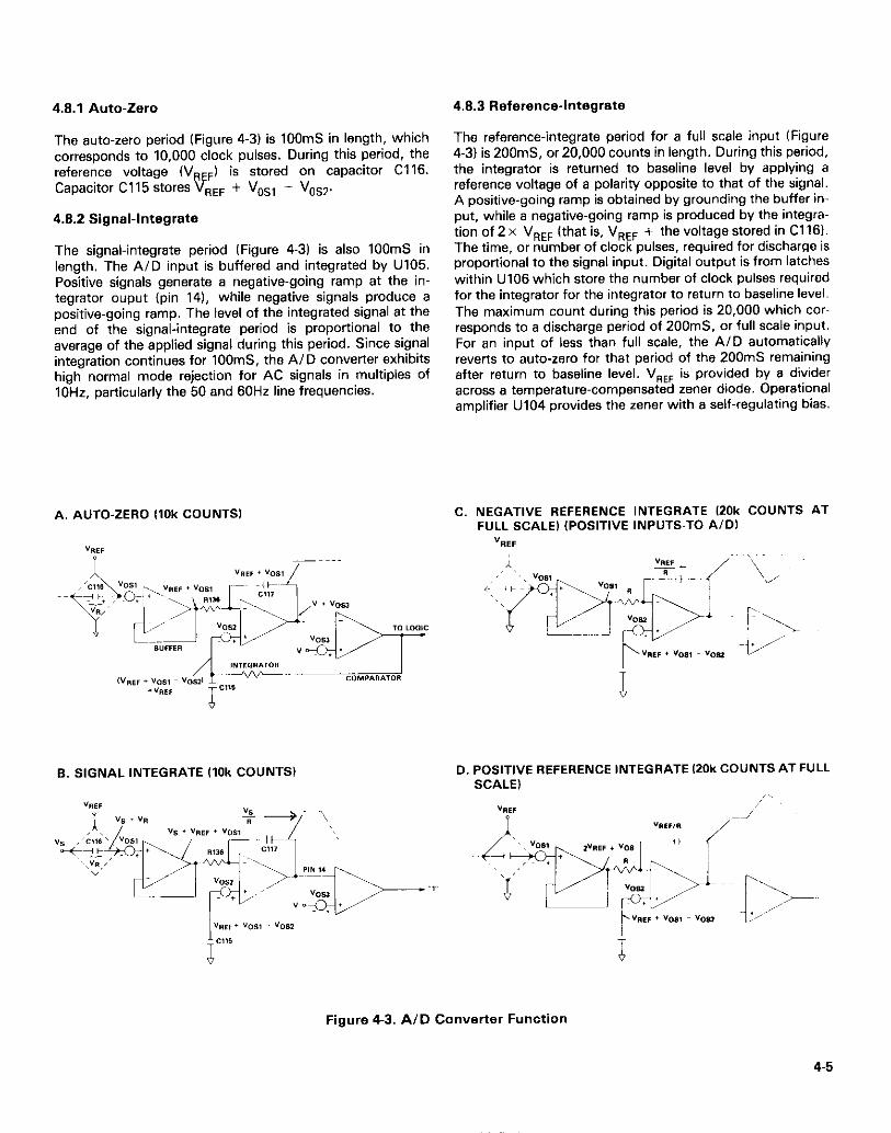
4.8.1 Auto-Zero 4.8.3 Reference-Integrate
The auto-zero period (Figure 4-3) is 1OOmS in length, which corresponds to 10,000 clock pulses. During this period, the reference voltage W,,,) is stored on capacitor Cl% Capacitor Cl15 stores V,,, + V,,, - V,,,.
4.82 Signal-Integrate
The signal-integrate period (Figure 4-3) is also 1OOmS in length. The A/D input is buffered and integrated by U105. Positive signals generate a negative-going ramp at the in- tegrator ouput (pin 14). while negative signals produce a positive-going ramp. The level of the integrated signal at the end of the signal-integrate period is proportional to the average of the applied signal during this period. Since signal integration continues for 100mS. the A/D converter exhibits high normal mode rejection for AC signals in multiples of IOHz, particularly the 50 and 60Hz line frequencies.
The reference-integrate period for a full scale input (Figure 4-3) is ZOOmS, or 20,000 counts in length. During this period, the integrator is returned to baseline level by applying a reference voltage of a polarity opposite to that of the signal. A positive-going ramp is obtained by grounding the buffer in- put, while a negative-going ramp is produced by the integra- tion of 2 x V,,, (that is, V,,, + the voltage stored in Cl 16). The time, or number of clock pulses, required for discharge is proportional to the signal input. Digital output is from latches within U106 which store the number of clock pulses required for the integrator for the integrator to return to baseline level. The maximum count during this period is 20,000 which cor- responds to a discharge period of 200mS. or full scale input. For an input of lass than full scale, the A/D automatically reverts to auto-zaro for that period of the 200117s remaining after return to baseline level. V,,, is provided by a divider across a temperature-compensated zener diode. Operational amplifier U104 provides the zener with a self-regulating bias.
C. NEGATIVE REFERENCE INTEGRATE IZOk COUNTS AT FULL SCALEI (POSITIVE INPUTS-TO AID)
6. SIGNAL INTEGRATE llOk COUNTS) D. POSITIVE REFERENCE INTEGRATE IZOk COUNTS AT FULL SCALE)
Figure 4-3. A/D Converter Function
4-5
4.9 DISPLAY
Five light-emitting diodes (LED) are driven by lJ203, which is a CMOS BCD-to-seven segment decoder/driver with bipolar current-sourcing outputs. Segment currents are. limited to ap- proximately 20mA peak by resistor network R202. The LED readout is a multiplexed, common-cathode configuration with Darlington array U202 sequentially sinking current from each digit. Blanking of the overrange digit is accomplished by gates UlO4C and U104D. U104A and U104B ensure that CMOS-compatible levels are maintained on U104D. regardless of the loading of U202. The minus polarity readout is blanked on AC voltage and resistance ranges by normally open contacts on the AC and 0 pushbuttons.
4.10 AC POWER SUPPLY
When the Model 177 is operated from AC line power, the power supply furnishes +5, + 15, and -15V from regulators VR,lOl, VR102 and VR103, respectively. Full-wave rectified AC from bridge rectifiers CR103 and CR104 is filtered by capacitors C120, Cl23 and Cl25 and is applied to the linear voltage regulators.
4.11 MODEL 1788 BAlTERY PACK
When the Model 1788 Battery Pack is installed in the Model 177. S102 must be set to the BAT position to provide addi- tional secondan/ voltage for battery charging. SlO2 also swit- ches the input to VRlOl from bridge rectifier CR103 to bat- teries BT301. Four 2V. 2.5 ampere-hour lead-acid calls supply approximately 9.8V at full charge. After six hours of use on battery power, the battery pack should be recharged to en- sure long battery life.
4.11.1 Battery Charging Circuit
While the Model 177 is plugged into line power and the bat- tery pack is installed, battery charging proceeds as follows: I, Full-wave rectified from CR103 is applied to the
anode of 0301, which is an SCR which regulates charg- ing voltage. When Q301 is triggered on by a sufficient gate-cathode voltage differential, the batteries receive charge. Charging continues as long as the bridge output voltage exceeds battery voltage by 1V or more. Resistor
R304 limits charging currant when recharging a set of completely discharge calls, a filtered positive output from CR104 (or T301) provides the necessary gate turn-on bias through I7306 and diode CR301. Resistor R303 ensures proper high-temperature operation of CI301.
2. When the battery voltages reach the present float voltages of 9.8V, zener VR301 conducts sufficient current to turn on Q302 and thus remove the gate trigger voltage from Q301. Float voltage is adjusted with R301. This is a factory adjustment which will normally not need field readjust- ment.
4.11.2 Battery Operation and Shutdown Circuit
The Model 177 operates as follows on battery power: I. When the power is turned on, the batteries are connected
to the input of VRlOl to supply + 5V for the logic, display and the clock circuit. The clock output is applied to the A/D converter as described in paragraph 4.7, and U301 which is a divide-by-four binary counter. The outputs of U301 drive a DC-to-DC inverter which is sychronized to the A/D converter to filter out inverter noise. The 25kHz operating frequency is optimal for the small transformer size and results in low switching losses. Blocking capacitors C301 and C302 protect 0307 and 0308 from damage if the drive is lost. Two half-wave rectifiers (CR304 and CR3051 on the secondary of T301 provide rectified AC to filter capacitors C304 and C305, which provide power to + 15 and -15V regulators VR102 and VR103, respectively.
2. To prevent permanent loss of battery capacity caused by deep discharge, a shutdown circuit stops operation on bat- tery power when the battery voltage drops below approx- imately 7.2V. Shutdown is performed by micropower voltage detector U302. The open-collector output (U302, pin 41 saturates low and turns off pass transistor Q309 when the input voltage (at U302. pin 31 drops below 1.15V (typical). Resistor R314 provides sufficient hysteresis to prevent discharge from resuming when the battery voltage rises following disconnection of the load.
4-6
SECTION 5 MAINTENANCE
5.1 INTRODUCTION
This section contains information necessary to maintain the Modal 177 and Model 1788 Battery Pack. Information con- cerning adjustment/calibration, troubleshooting, front panel zero knob removal and replacement, and fuse replacement are contained in this section. Calibration should be performed yearly (every 12 months) or whenever performance verifica- tion (see Section 3) indicates that the Model 177 is out of specifications. If any step in the calibration procedure cannot be performed properly, refer to troubleshooting information in this section, or contact your Keithley representative or the factory.
5.4.1 Calibrating Shield Installation
If the Modal 1788 Battery Pack is installed in the instrument it must be removed and the calibration shield reinstalled before calibration. If the calibration shield has been lost or mis- placed, order Keithley Part Number 29473.
WARNING Disconnect the line cord before removing the cese cover.
1. Turn off the power and disconnect the line cord. Remove four screws from the bottom of the case and separate the top cover from the bottom cover.
2. Push back the ground clip from the upper side of the bat- ten/ pack and remove the battery pack from the spacers.
3. Calibration may be performed on battery power as long as the battery pack is sufficiently charged. Leave the battery pack plugged into the instrument, but set the battery pack behind the Model 177 on the bench or table. Ensure fhaf LINE/BAT switch lS102) is in BAT position.
4. Set the calibration shield in place on the spacers. The shield should read correctly when viewed from the front of the instrument.
5. Slide the ground clip over the top of the calibration shield so that it contacts the upper surface of the shield.
6. If the battery power is not to be used, plug in the line cord and position S102 to the LINE position if the batten, pack has been disconnected.
5.4.2 Warm-Up
Turn the Model 177 on and allow a one hour warm-up time.
5.4.3 Calibration Instructions
WARNING Some procedures require the use of high voltage. Take cere to prevent contact with live circuits which could ceuse electrical shock resulting in injury or death. Use en in- sulated tool when meking adjustments.
NOTE Calibration should be performed by qualified personnel using accurate and reliable test equip- ment.
5.2 RECOMMENDED TEST EQUIPMENT
Recommended test equipment for calibration is listed in Table 5-1. Alternate test equipment may be used. However, the ac- curacy of the alternate test equipment must be at least 10 times better than the Model 177 specifications, or equal to Table 5-l specifications.
5.3 ENVIRONMENTAL CONDITIONS
Calibration should be performed under laboratory conditions having an ambient temperature of 20°C to 26’C (68’F to 78°F). and a relative humidity of lass than 80%. If the instru- ment has been subjected to temperatures outside of this range, or to higher humidity, allow one hour minimum for the instrument to stabilize at the specified environmental condi- tions before beginning the calibration procedure.
5.4 CALIBRATION PROCEDURE
Perform the following adjustments to calibrate the Model 177 and restore its operation to specified limits.
Table 5-1. Recommended Test Equipment For Calibration
AC Calibrator
Decade Resistor 1OOR Per Step 4-Terminal Low Thermal Resistor
Specification O.lV, 1v. 1ov. 1oov. 1ooov f0.002% O.lV, lV, 1ov. 1oov. fO.Ol% 5000, 1.9kQ. 190k0. *O.Ol% 1O:l divider within 50 PPM (See Figure 3-l) !
Mfr. Fluke
Fluke
ESI ESI
Model 343A
5200A
RS725 SRlOlO
5-l
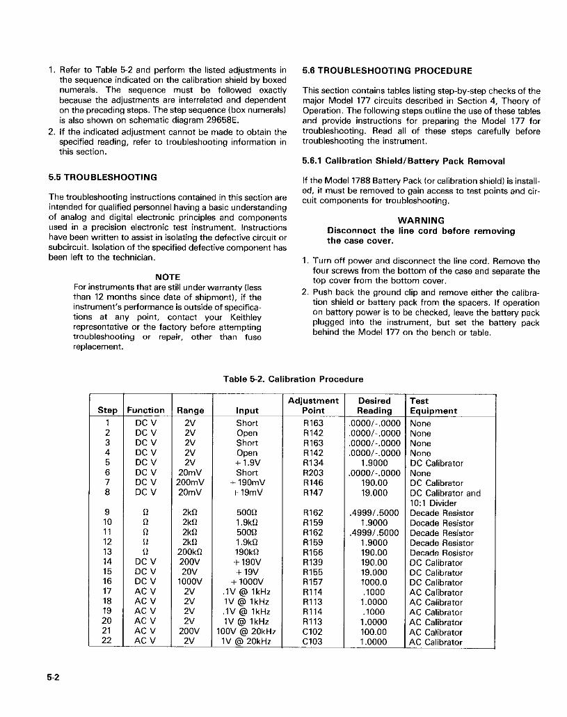
1. Refer to Table 5-2 and perform the listed adjustments in the sequence indicated on the calibration shield by boxed numerals. The sequence must be followed exactly because the adjustments are interrelated and dependent on the preceding steps. The step sequence (box numerals) is also shown on schematic diagram 29658E.
2. If the indicated adjustment cannot be made to obtain the specified reading, refer to troubleshooting information in this section.
5.5 TROUBLESHOOTING
The troubleshooting instructions contained in this section are intended for qualified personnel having a basic understanding of analog and digital electronic principles and components used in a precision electronic test instrument. Instructions have been written to assist in isolating the defective circuit or subcircuit. Isolation of the specified defective component has been left to the technician.
NOTE For instruments that are still under warranty (less than 12 months since date of shioment). if the instrument’s performance is outside of specifica- tions at any point, contact your Keithley representative or the factory before attempting troubleshooting or repair, other than fuse replacement.
5.6 TROUBLESHOOTING PROCEDURE
This section contains tables listing step-by-step checks of the major Model 177 circuits described in Section 4. Theory of Operation. The following steps outline the use of these tables and provide instructions for preparing the Model 177 for troubleshooting. Read all of these steps carefully before troubleshooting the instrument.
5.6.1 Calibration Shield/Battery Peck Removal
If the Model 1788 Battery Pack (or calibration shield) is install- ed, it must be removed to gain access to test points and cir- cuit components for troubleshooting.
WARNING Disconnect the line cord before removing the case cover.
1. Turn off power and disconnect the line cord. Remove the four screws from the bottom of the case and separate the top cover from the bottom cover.
2. Push back the ground clip and remove either the calibra- tion shield or battery pack from the spacers. If operation on battery power is to be checked, leave the battery pack plugged into the instrument, but set the battery pack behind the Model 177 on the bench or table.
Table 5-2. Calibration Procedure
Step :unction Range Input 1 DC v 2v Short 2 DC v 2v Open 3 DC v 2v Short 4 DC v 2v Open 5 DC V 2v f1.9V 6 DC V 20mV Short 7 DC V !OOmV + 190mV 8 DC V 20mV + 19mV
Adjustment Point R163 R142 R163 R142 R134 R203 R146 R147
Desired Reading
oooo/-.oooo oooo/-.oooo oooo/-.oooo oooo/-.oooo
1.9000 3000/-.oooo
190.00 19.000
9 n 2k!l 50011 R162 4999/.5000 10 0 2kfl 1.9kn R159 1.9000 11 0 2kfl 5oon R162 4999/.5000 12 0 2kfl 1.9k0 R159 1.9000 13 n 200kn 190kR R156 190.00 14 DC V 2oov + 19ov R139 190.00 15 DC V 2ov -+ 19v R155 19.000 16 DC v 1ooov + 1ooov R157 1000.0 17 AC V 2v .lV @ 1kHz R114 .lOOO 18 AC V 2v IV @ lktlz R113 1 .oooo 19 AC V 2v .lV @I 1kHz R114 .lOOO 20 AC V 2v 1V @ 1kHr R113 1 .oooo 21 AC V 2oov IOOV @ 20kHr Cl02 100.00 22 AC V 2v 1V @ 20kHz Cl03 1 .oooo
Test Equipment None None None None DC Calibrator None DC Calibrator DC Calibrator and 1O:l Divider Decade Resistor Decade Resistor Decade Resistor Decade Resistor Decade Resistor DC Calibrator DC Calibrator DC Calibrator 4C Calibrator 4C Calibrator 4C Calibrator 4C Calibrator 4C Calibrator .4C Calibrator
5-2
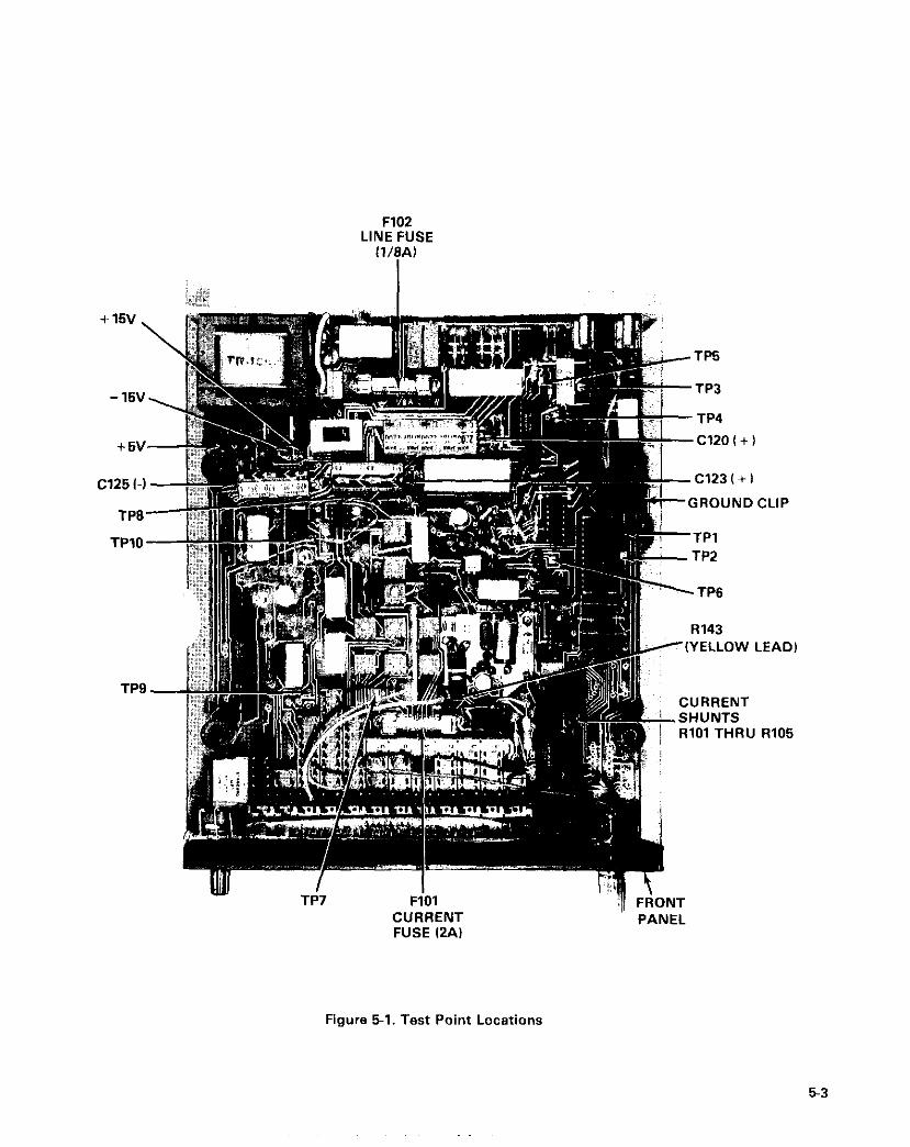
F102 LINE FUSE
(1/8A)
+15v,
-15v
+5v
Cl25 I-1
TPS’
TPlO’
TPS
&..-- TP5
FiOl CURRENT FUSE (2A)
R143 -(YELLOW I
CURRENT .SHUNTS RlOl THRU
PANEL
CLIP
LEAD)
RlOS
Figure 5-l. Test Point Locations
53
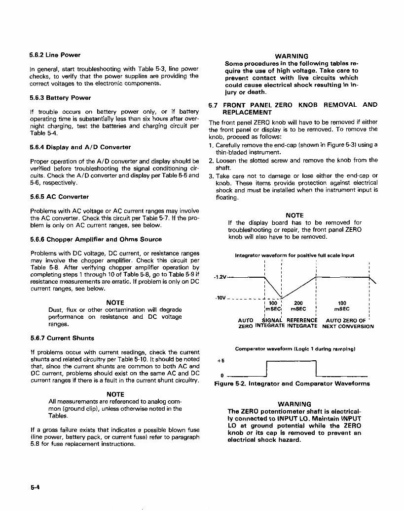
5.6.2 Line Power
In general, start troubleshooting with Table 5-3, line power checks, to verify that the power supplies are providing the correct voltages to the electronic components.
5.6.3 Battery Power
If trouble occurs on battery power only, or if battery operating time is substantially less than six hours after over- night charging, test the batteries and charging circuit per Table 5-4.
5.6.4 Display and A/D Converter
Proper operation of the AID converter and display should be verified before troubleshooting the signal conditioning cir- cuits. Check the A/D converter and display per Table 5-5 and 5-6, respectively.
5.6.5 AC Converter
Problems with AC voltage or AC current ranges may involve the AC converter. Check this circuit per Table 5-l. If the pro- blem is only on AC current ranges, see below.
5.6.6 Chopper Amplifier and Ohms Source
Problems with DC voltage, DC current, or resistance ranges may involve the chopper amplifier. Check this circuit per Table 5-8. After verifying chopper amplifier operation by completing steps 1 through 10 of Table 5-8, QO to Table 5-9 if resistance measurements are erratic. If problem is only on DC current ranges, see below.
NOTE Dust, flux or other contamination will degrade performance on resistance and DC voltage ranges.
5.6.7 Current Shunts
If problems occur with current readings, check the current shunts and related circuitry per Table 5-10. It should be noted that, since the current shunts are common to both AC end DC current, problems should exist on the same AC and DC current ranges if there is a fault in the current shunt circuitry.
NOTE All measurements are referenced to analog com- mon (ground clip), unless otherwise noted in the Tables.
If a gross failure exists that indicates a possible blown fuse (line power, battery pack, or current fuse) refer to paragraph 5.8 for fuse replacement instructions.
WARNING Some procedures in the following tables re- quire the use of high voltege. Take cere to prevent contact with live circuits which could reuse electrical shock resulting in in- jury or death.
5.7 FRONT PANEL ZERO KNOB REMOVAL AND REPLACEMENT
The from panel ZERO knob will have to be removed if either the front panel or display is to be removed. To remove the knob, proceed as follows: 1, Carefully remove the end-cap (shown in Figure 5-31 using a
thin-bladed instrument. 2. Loosen the slotted screw and remove the knob from the
shaft. 3. Take care not to damage or lose either the end-cap or
knob. These items provide protection against electrical shock and must be installed when the instrument input is floating.
NOTE NOTE If the display board has to be removed for If the display board has to be removed for troubleshooting or repair, the front panel ZERO troubleshooting or repair, the front panel ZERO knob will also have to be removed. knob will also have to be removed.
-1.2" n
I
-,o"-~----~- I
( 100 ; ,
200 I 100 ImSEC!
/ InSEC I mSEC I
AUTO ShGNA; REFERENC: AUTO ZERO OF ! ZERO INTEGRATE INTEGRATE NEXT CONVERS,ON
Comparstor waveform Logic 1 during ramping)
‘L-J-l--
Figure 5-2. Integrator end Comparator Waveforms
WARNING The ZERO potentiometer shaft is electrical- ly connected to INPUT LO. Maintain INPUT LO et ground potential while the ZERO knob or its cep is removed to prevent en electrical shock hazard.
5-4
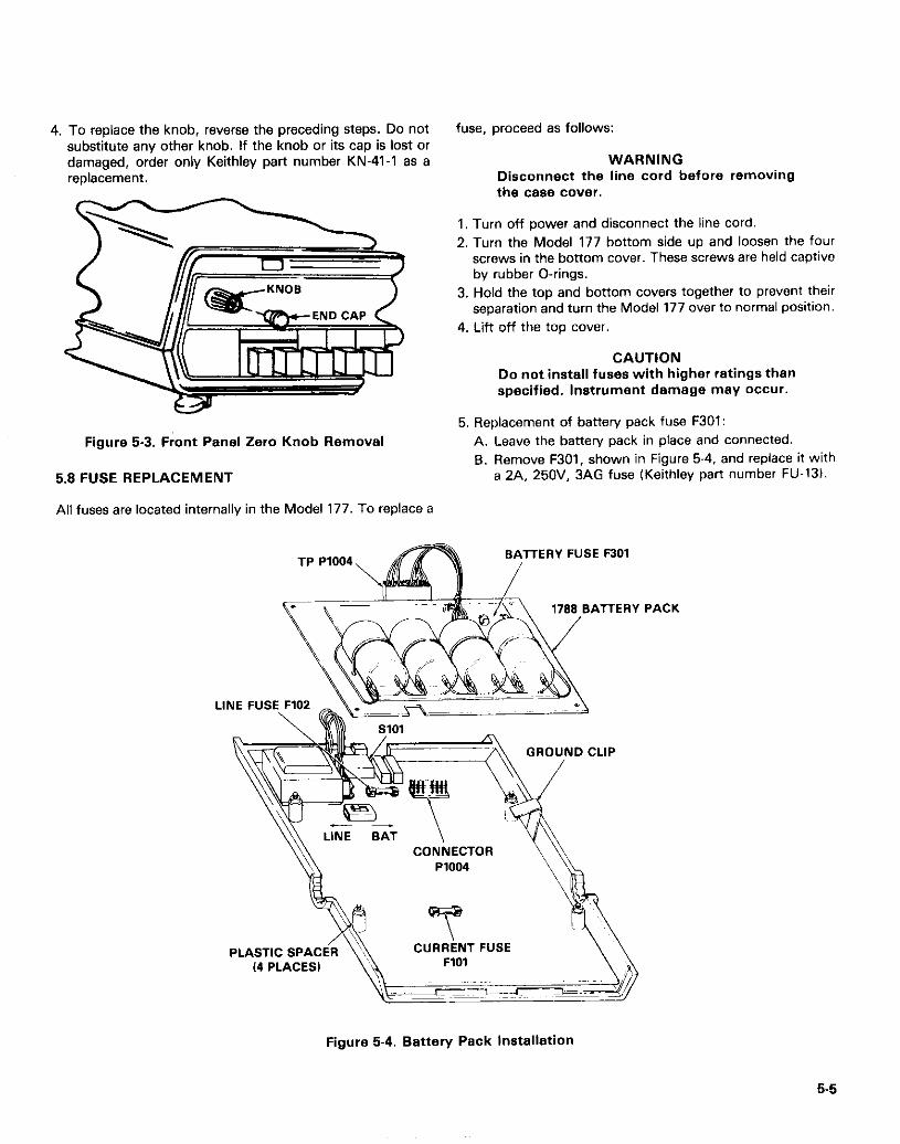
4. To replace the knob, reverse the preceding steps. Do not substitute any other knob. If the knob or its cap is lost or damaged, order only Keithley part number KN-41-l as a replacement.
Figure 5-3. F&t Panel Zero Knob Removal
5.8 FUSE REPLACEMENT
All fuses are located internally in the Model 177. To replace a
fuse, proceed as follows:
WARNING Disconnect the line cord before removing the caaa cover.
1, Turn off power and disconnect the line cord.
2. Turn the Model 177 bottom side up and loosen the four screws in the bottom cover. These screws are held captive by rubber O-rings.
3. Hold the top and bottom covars together to prevent their separation and turn the Modal 177 over to normal position.
4. Lift off the top covar.
CAUTION Do not install fuses with higher ratings than specified. Instrument damage may occur.
5. Replacement of battery pack fuse F301: A. Leave the battery pack in place and connected.
B. Remove F301, shown in Figure 5-4, and replace it with a ZA, 25OV. 3AG fuse (Keithley part number FU-131.
E&,\ 1788,BATTERV
BAITERV FUSE F301
LINE FUSE FlOZ
\\ CONiUECTOR \\
PACK
Figure 5.4. Battery Pack Installation
5-5
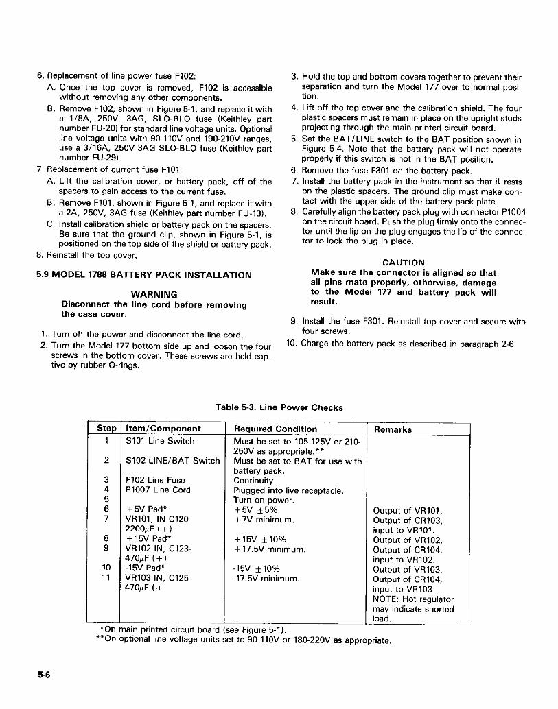
6. Replacement of line power fuse F102: A. Once the top cover is removed, FlO2 is accessible
without removing any other components. B. Remove FIOZ, shown in Figure 5-l. and replace it with
a l/EA, 25OV. 3AG. SLO-BLO fuse (Keithley part number FU-201 for standard line voltage units. Optional line voltage units with 90.IIOV and 190.2lOV ranges, use a 3/16A, 250V 3AG SLO-BLD fuse (Keithley part number FU-291.
7. Replacement of current fuse FlOl:
A. Lift the calibration cover, or battery pack, off of the spacers to gain access to the current fuse.
B. Remove FIOI, shown in Figure 5-l. and replace it with a ZA, 25OV, 3AG fuse (Keithley part number FU-13).
C. Install calibration shield or battery pack on the spacers. Be sure that the ground clip, shown in Figure 5-l. is positioned on the top side of the shield or battery pack.
8. Reinstall the top cover.
5.9 MODEL 1788 BA-ITERY PACK INSTALLATION
WARNING Disconnect the line cord before removing the case ccwar.
1. Turn off the power and disconnect the line cord. 2. Turn the Model 177 bottom side up and loosen the four
screws in the bottom cover. These screws are held cap- tive by rubber O-rings.
3. Hold the top and bottom covers together to prevent their separation and turn the Model 177 over to normal posi- tion.
4. Lift off the top cover and the calibration shield. The four plastic spacers must remain in place on the upright studs projecting through the main printed circuit board.
5. Set the BAT/LINE switch to the BAT position shown in Figure 5-4. Note that the battery pack will not operate properly if this switch is not in the BAT position.
6. Remove the fuse F301 on the battery pack. 7. Install the battery pack in the instrument so that it rests
on the plastic spacers. The ground clip must make con- tact with the upper side of the batten/ pack plate.
8. Carefully align the battery pack plug with connector P1004 on the circuit board. Push the plug firmly onto the connec- tar until the lip on the plug engages the lip of the connec- tar to lock the plug in place.
CAUTION Make sure the connector is aligned so that all pins mate properly, otherwise, damage to the Modal 177 and battery pack will result.
9. Install the fuse F301. Reinstall top cover and secure with four screws.
10. Charge the battery pack as described in paragraph 2.6.
Table 5-3. Line Power Checks
step Item/Component 1 SIOI Line Switch
2 SIOZ LINE/BAT Switch
F102 Line Fuse PI007 Line Cord
8 9
10 11
+ 5V Pad* VRlOl, IN CIZO- 22OO~F ( + ) + 15V Pad* VR102 IN, C123- 47OpF I+ j -15V Pad* VR103 IN, Cl25. 17OpF I-)
<On in ain printed circuit board (St **On optional line voltage units se
Required Condition Must be set to 105.125V or 210. 250V as appropriate.** Must be set to BAT for use with batten/ pack. Continuity Plugged into live receptacle. Turn on power. +5v *5% + 7V minimum.
+15v *lo% + 17.5V minimum.
-15v flO% -17.5V minimum.
Remarks
Output of VRlOl. Output of CR103, input to VRlOl. Output of VRIOZ, Output of CR104, input to VRIOZ. Output of VR103. Output of CR104, input to VR103 NOTE: Hot regulator may indicate shorted load.
?a Figure 5-l). t to 90-I IOV or 180.22OV as appropriate.
5-6
Table 5-4. Battery Power Checks
step 1 2 3 4 5
Item/Component
S102 LINE/BAT Switch PI007 Line Cord F301
5A BT301 Batteries
Each battery cell 1.5-3V for any cell. voltage during charging. 0301 Anode Full wave rectified voltage, 15 VDC
nominal. c304 + + 17.5V minimum.
PI004 pin 8 or U301
12A
13 14
15
0307 and 0308 Base Q307, Q308 Collector
Required Condition Check AC line power per Table 5-3. Turn off power. Move to BAT. Plugged into live receptacle. Remove fuse and connect ammeter to fuse clip 0 to 500mA charging rate, varies with line voltage and battery state of charge. Full charge is =9.8V over 4 cells. R301 adjusts charging rata (float voltage)
Should saturate only when battery approaches full charge. 8.2V zenar. Unplug line cord Et turn power on. IOOkHz 5V square wave.
+ 7V minimum
Square wave, f0.7V at 25kHz. Must oscillate from saturation to twice battery voltage (= 19V) at 25kHz f 17.5V minimum ( *25V typical with fully charged bat.)
Remarks
Charge circuit checks. No charge, see step 5A. Correct charging but short battery operating time, see step 6. If voltage is low and adjusts ment of R301 does not start charging, see steps 7 and following. If voltage is low and adjustment of R301 does start charging, see Table 5-l 1 for adjust- ment of battery charge voltage. High voltage or zero indi- cates damaged cell. Output of CR103
Output of CR104. Triggers Q301 gate thru R306 and CR301 unless Q302 is on.
Discharge checks. Clock input. If no input, see step 12A. Battery voltage input to VRlOl. Output of u301, -4 lnverier
lnverter Output, input to VRIOZ and VR103
57
Table 6-5. Display Checks
Step Item/Component Required Condition Remarks 1 Turn on power. Any function
or range, except OHMS. 2 +5V Pad* or JIOOI, +5v *5% If low, check per Table
pin 7 5-3 3 U202, pins 2, 6, 7, Digit drive. Low = Enabled LED Cathode
9 and 13 4 Ki3; pins 1, 2, 6 HI = Enabled BCD input to U203 seg-
ment decoder/drive 5 U203, pin 2 Negative-going signal lasting Leading digit suppres-
for 200 clock pulses. sion. 6 JIOOI, pin 2 Polarity Line (sign) Polarity output is dis-
HI = Off abled on AC an a. LO = -
7 JIOOI, pin 4 Appropriate DP line high (on). Depress RANGE push- J1002, pins 1, 11 & 12 buttons to check all
DPs.
‘On main printed circuit board. See Figure 5-l
Table 5-6. A/D Converter Checks
St;p 1 Item/Component
2 Display 3 TPI *
4 TPZ* 5
6 Display
7 TP4*
8 TP3* 9 U105, pin 11
10 U105, pin 14
1: U105, U105, pin pin 9 13
13 External Voltage Source.
14 Display
15 TPl 16 U105, pin 14 17 U105, pin 2
*On main printed circuit board, see Figure 5.1,
+ l.OOV Shot? TPI to TP2.
1 .OOOO k2 digits
0 to + 5V square wave at IOOkHz f IOOHz. +1.0 *O.lV +1.0 *0.1v
-1.2 f0.2V
+1v +1v Apply + 1.9OOOV
1.9000 * 1 Digit
Remarks
Input to U106. Chopper out- ’ put.
Reference output. Connects reference output to U106 input. If steps 4 and 6 are correct AID converter is functioning properly. If not, continue with step 7. Clock input to U106.
Stored autozero voltage. X-node voltage to integrator in U105. U105 integrator output voltage. U105 buffer input. U105 buffer output. Calibration point.
If different, check U106 input. Input to U106. Integrator output. Comparator output.
5-8
Table 5-7. AC Converter Checks
step 1
Item/Component Required Condition Turn on power. Select 2VAC range.
2
3
External voltage source. TPlO*
4pply IV rms at 1 kHz,
.99V rms nominal
4
5
TPEX
U103 Pin 6 or TPl*
.993V rms nominal.
+1v
6 External voltage Select 20VAC range. Apply IOV source. rms at 1 kHz.
7 TPIO .099V rms nominal.
8 9
TP8 .993V rms nominal. External voltage Select IOOOVAC range. Apply SOUKB. IOOOOV rms at 1 kHz.
10 TPlO .99V rms nominal.
11
12
External voltage Select 200VAC range. Apply IOOV SOUKB. rms at 20kHz. Display 100.00 nominal.
13
14
External voltage source. Display
Select 2VAC range. Apply IV rms at 20kHz. 1 .OOOO nominal
15
16
External voltage Select IOOOVAC range. Apply SO”Kt?. IOOOV rms at 20kHz. Display 1000.0 * nominal.
17
18
External voltage Select 2VAC range. Apply IV SOWCC?. rms at 45Hz. Display l.OOOOV * nominal.
-
Remarks
VOTE: Full scale input on 311 ranges should produce = 2V rms output at TP8’. Calibrated input.
Dutput of UlOl and faed- back components R108 and Cl03 (nominal gain ,991. output of u102. IQ102 on, nominal gain 1.0031. Output of U103. Gain of U103 adjusted to provide + 1VDC output for 1VAC I ‘h scale) input. Gain check of UIOI and U102. Nominally, .0099 IUlOl) and 10.03 lUlO21. Output of UlOl and feed- back components R109. Cl04 and Cl101 Ion). Output of u102 (Q102 off). Calibrated input. Check gain of UlOl (nominal .00099). Output of UlOl and feed- back components KlOl, RI10 and Cl05 KIOI (Closed). Calibrated input.
High frequency response (compensation C102, C103, ClO4). Calibrated input.
High frequency response. (Compensation C102, c1031.
High frequency response. IC;yansation C102, C103.
Low frequency response. ClOl, C106, C107, C108, c109.
*See Figure 5-l.
5-9
Table 5-8. DC Attenuation end Chopper Amplifier Checks
Step 1
ltemlComponent Required Condition Turn on power. Select 20mVDC range. Short input end adjust F.P. Zero for + .OOOO on display.
2 TP5. TP6” =-7.5V DC (on DMM).
3
4
External voltage source. RI43 (yellow wire slide)“.
Apply + 19mV. Calibrated input.
+ 19mV.
5
6
7
8
9
10
11
12
13
14
15
16
TPl* + 1.9v
External voltage Select 200mVDC range. Apply. source. + 190mV. RI43 + 190mV
TPl +1.9v
External voltage Select 2VDC range. Apply source. + 1.9v. R143, TPl +1.9v
External voltage Select 20VDC range. Apply source. + 19v. R143 +1.9v
External voltage Select 200VDC range. Apply source. + 19ov. R143 +1.9v
I External voltage Select 1OOOV (12OOVI DC source. range. Apply + IOOOV. RI43 +1v
*On maln pnnted circuit board, see Figure 5-l.
Remarks NOTE: Insufficient zero adjustment may indicated leaky FET switches in Chopper Amplifier Circuit. Chopper Drive. Signals are actually 0 to -15 square waves et 390Hz. A steady zero volt or -15V signal indicates a problem in the chopper drive or clock circuitry.
Input to chopper amplifier + 1 attenuation (range resistors). Input to U106, chopper output ( x 100 gain). Calibrated input,
Input to chopper amplifier + 1 attenuation. Input to U106, chopper output t x 10 gain). Calibrated input.
+ 1 attenuation, x 1 chop- per gain. Calibrated input.
f 10 attenuation (range resistors). Calibrated input.
f 100 attenuation (range resistors). Calibrated input.
+ 1000 attenuation (range resistors).
5-10
Table 5-9. Ohms Source end Resistor Checks
Display 4 TP9”
5 INPUT HI to LO
6 INPUT HI to LO
7 1.9kl7 resistor. 8 Display
9 19kR resistor. 10 Display
11 190kC resistor. 12 Display
13 1900kD resistor. 14 Display
15 1OMD resistor 16 Display
..w’IY..Y” -.,..“...-..
Check chopper amplifier operation per Table 5-7, steps 1 thru 10. Select 2kD range. Short Input. .OOOO *I digit. -IV Approximately
Remove short end connect ammeter from INPUT HI to LO. Source current should be approximately ImA, HI terminal negative. Remove ammeter end measure open circuit voltage. Voltage must be -2 to -5v. Apply to INPUT. 1.9000 * 12 digits.
Apply to INPUT. Select 20kD range. 19.000 -f 12 digits.
Apply to INPUT. Select 200kR range. 190.00 f 12 digits.
Apply to INPUT. Select 2000kR range. 1900.0 f 12 digits.
Apply to INPUT. Select 20MI2 range. 10.000 * 12 digits.
NOTE: Reference loading by the ohms source does not affect D readout since AID converter is ratiometric.
I *See Figure 5-l.
Table 5.10. Current Shunt Checks
Step Item/Component Required Condition F
..” ..-...-
Inverted reference voltage plus calibrated offset of u107. If incorrect, check R158 end switching to INPUT HI end chopper amplifier.
HI negative with respect to LO. Display should be blink- ing, indicating overrange. Calibrated resistance. Subtract test lead resistance from reading. Checks accuracy of R158 and feed- beck loop to U107. Calibrated resistance. Source resistors: RI56 R154 (6975kDl. R157 (wiper). Calibrated resistance. Source resistors: R158, RI57 R156 (wiper), R154 l89.75kC. 8.975M). Calibrated resistance. Source resistors: R158, R157. R156. RI55 fwiperl. R154, (all except 6975MRl. Calibrated resistance. Source resistors: all R range resistors. NOTE: To con- veniently measure the resis- tance of all D range resistors, turn power off, set all function switches out end measure resistance INPUT HI to LO. .___
Remarks
L Apply a known % scale current end measure voltage across shunt.
( Cl;;ping must occur et
5-11
Table 5-11. Adjustment of Battery Charae Voltaae
lponent Required Condition Instrument off. Turn full CCW (maximum charge
1 rate). Monitor banery voltage for’9.8V.
When cells reach 9.8V, turn DMM on and adjust to maintain 9.8V across BT301.
Remarks
Fully charged cells require several minutes to reach this level. Dis- charged cells require several hours.
CAUTION Charging to 7 1OV for longer than 30 minutes will reduce battery life.
5-12
SECTION 6 REPLACEABLE PARTS
6.1 INTRODUCTION 6.4 FACTORY SERVICE
This section contains information for ordering replacement If the instrument is to be returned to the factory for sarvice.
parts. please complete the service form which follows this section end return it with the instrument.
6.2 PARTS LISTS 6.5 COMPONENT LOCATION DRAWINGS
Table 6-2 contains a list of parts for the Model 177 mother board, Table 6-3 lists display board parts, end Table 6-4 lists 1. Model 177 PC-476 Component Layout No. 29474D. parts for the optional Modal 1766 Batten/ Pack. Each list is ai- 2. Display Board PC-475 Component Layout No. 29652C. ranged in alphabetical order according to circuit designation. Mechanical parts ere listed on Figure 6-l.
3. Model 1766 Battery Peck PC-451 Component Layout No. 29007c.
6.3 ORDERING INFORMATION 6.6 SCHEMATIC DIAGRAMS
To place en order or to obtain information concerning replacement parts, contact your Keithley representative or
1. Model 1766 Battery Peck: Schematic No. 29659C.
the factors. See the inside front cover for addresses. When 2. Model 177 4% Digit Multimeter: Schematic No. 29656E.
ordering, include the following information: I. Instrument Model Number. 2. Instrument Serial Number. 3. Pert Description. 4. Circuit Designation (if applicable).
5. Keithley Pert Number.
6.7 MAINTENANCE KIT
A maintenance kit is available that contains a complement of spare parts that will maintain up to ten Model 177s. Specify Model 1779 Spare Parts Kit when ordering. A list of the kit parts is given in Table 6-l.
6-1
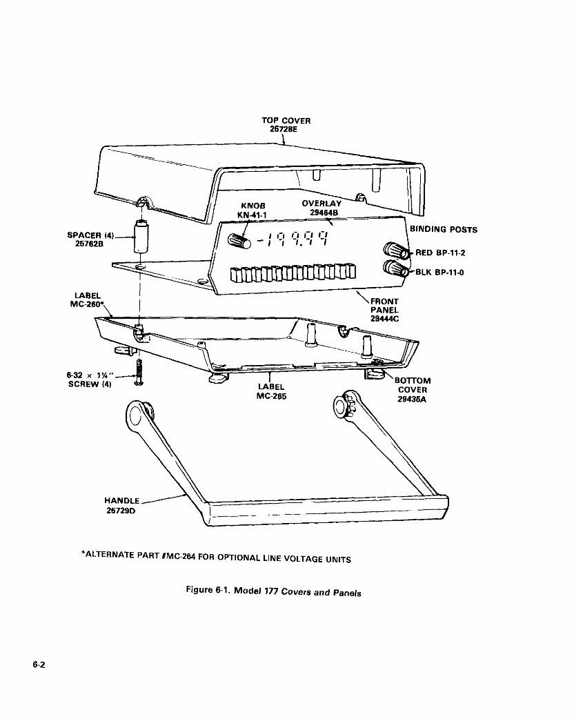
TOP COVER 26729E
KNH.1 294848 -4.u
BINDING PO1 STS
^ - - - - _ _
ELK BP-110
LABEL I \\,I
PI 3c
3ONT 4NEL
A444C
/-
832 x 1 SCREW I41 84 LAblEL
MC-265
HANDLE 26729D
‘ALTERNATE PART #MC-264 FOR OPTIONAL LINE VOLTAGE UNITS
Figure 6-l. Model 177 Covers and Panels
6-2
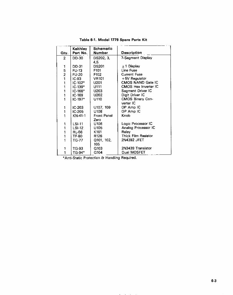
Table 6-1. Model 1779 Spare Parts Kit
my.
2
1 5 2 1 1 1 1 1 1
1 1 1
1 1 1 1 1
1 1
*An
T Keithley Part No. DD-30
DD-31 FU-13 FU-20 K-93 IC-102” IC-139” IC-168” IC-169 IC-197”
IC-203 IC-205 KN-41-1
LSI-11 LSI-12 RL-56 TF-80 TG-77
TG-93 TG-94” Q104
Static Protection Et Hand1
Schematic Number DS202, 3, 4,5 DS201 FlOl F102 Vi3101 u201 Ulll U203 u202 UllO
u107, 109 U108 Front Panel zero U106 u105 KlOl R126 0101, 102, 105 Q103
ing
Description 7-Segment Display
+ 1 Display Line Fuse Current Fuse + 5v Regulator CMOS NAND Gate IC CMOS Hex lnverter IC Segment Driver IC Digit Driver IC CMOS Binary Con- verter IC OP Amp IC OP Amp IC Knob
Loaic Processor IC An&a Processor IC Relay - Thick Film Resistor 2N4392JFET
2N3439 Transistor Dual MOSFET
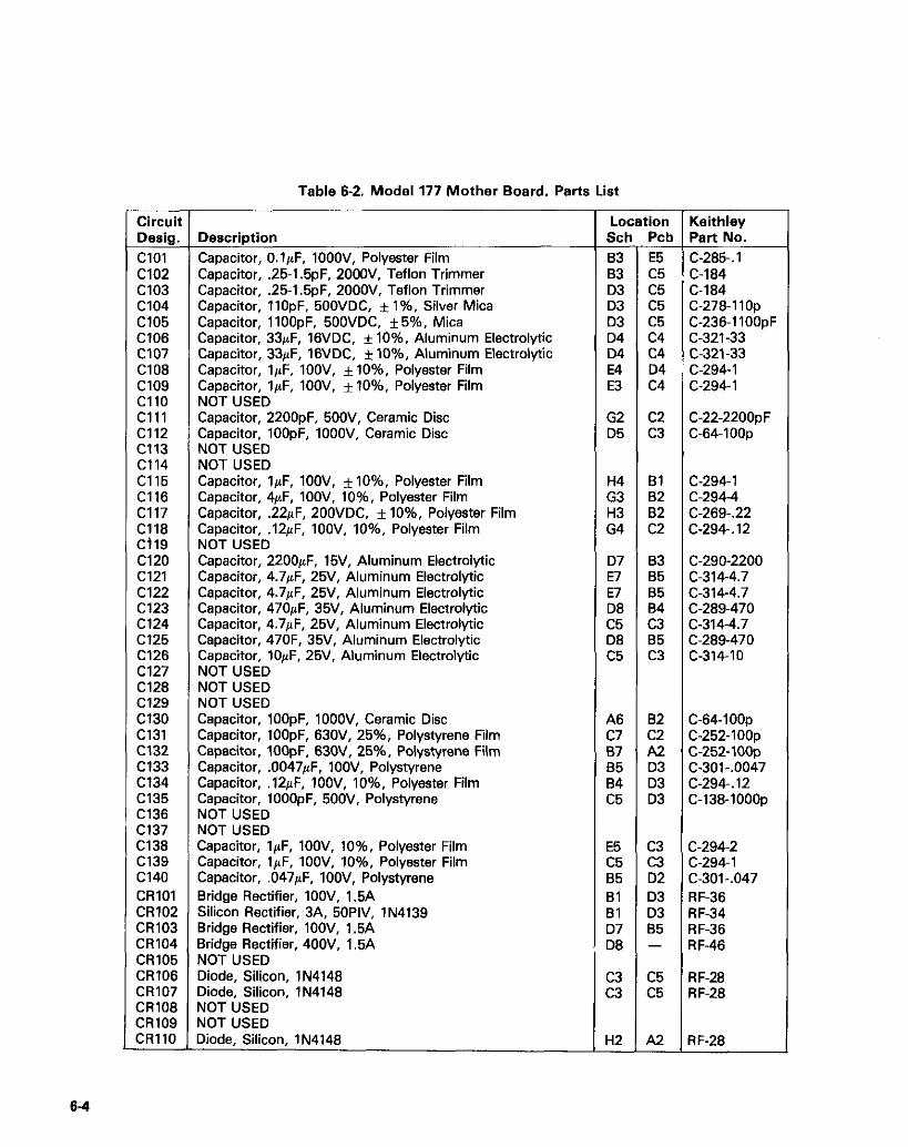
Table 6-2. Model 177 Mother Board. Parts List
Circui Desig. Cl01 Cl02 Cl03 Cl04 Cl05 Cl06 Cl07 Cl08 Cl09 Cl10 Cl11 Cl12 Cl13 Cl14 Cl 15 Cl16 Cl17 Cl18 Cl19 Cl20 Cl21 Cl22 Cl23 Cl24 Cl25 Cl26 Cl27 Cl28 Cl29 Cl30 Cl31 Cl32 Cl33 Cl34 Cl35 Cl36 Cl37 Cl38 Cl39 Cl40 CR101 CR102 CR103 CR104 CR105 CR106 CR107 CR108 CR109 CR110
Description Capacitor, O.lpF, 1OOOV. Polvester Film Cabacitor; .25L115pF, ZO~bOV,.Teflon Trimmer Capacitor, .25-l .5pF, ZOOOV, Teflon Trimmer Capacitor, IlOpF, 500VDC. f 1%. Silver Mica Capacitor, 11OOpF. 500VDC, *5%, Mica Capacitor, 33pF. 16VDC. f 10%. Aluminum Electrolytic Capacitor, 33~F, 16VDC, f lo%, Aluminum Electrolytic Capacitor, 1pF. lOOV, f 10%. Polyester Film Capacitor, lfiF, 1OOV. + 10%. Polvester Film NOT USED Capacitor, 22OOpF. 5OOV. Ceramic Disc Capacitor, 1OOpF. 1OOOV. Ceramic Disc NOT USED NOT USED Capacitor, lpF, 1OOV. f lo%, Polyester Film Capacitor, 4pF. 1OOV. 10%. Polyester Film Capacitor, .22pF, ZOOVDC, f lo%, Polyester Film Capacitor, .lZhF, lOOV, 10%. Polyester Film NOT USED Capacitor, ZZOOpF, 15V. Aluminum Electrolvtic Capacitor, 4.7pF. 25V, Aluminum Electrolytic Capacitor, 4.7pF. 25V, Aluminum Electrolvtic Capacitor, 470/~F, 35V. Aluminum Electrolytic Capacitor, 4.7/rF. 25V. Aluminum Electrolvtic C&∨ 47bF.’ 35V; Aluminum Electrolytic Capacitor, 1OpF. 25V. Aluminum Electrolytic NOT USED NOT USED NOT USED Capacitor, 1OOpF. lOOOV, Ceramic Disc Capacitor, 1OOpF. 63OV, 25%. Polystyrene Film Capacitor, IOOpF, 63OV, 25%. Polystvrene Film Capacitor, .0047&F, lOOV, Polystyrene Capacitor, .lZpF, IOOV, 10%. Polyester Film Capacitor, 1OOOpF. 5OOV. Polystyrene NOT USED NOT USED Capacitor, l+F, lOOV, 1096, Polyester Film Capacitor, lpF, 1OOV. 10%. Polyester Film Capacitor, .047pF, lOOV, Polystyrene Bridge Rectifier, 1OOV. 1.5A Silicon Rectifier, 3A. 5OPIV. lN4139 Bridge Rectifier, lOOV, 1.5A Bridge Rectifier, 4OOV, 1.5A NOT USED Diode, Silicon, lN4148 Diode, Silicon, lN4148 NOT USED NOT USED Diode, Silicon, IN4148
-
-
-
B3 D3 03 D3 D4 D4 E4 E3
G2 D5
Ei H3 G4
D7 E7 E7 D8 c5 D8 c5
A6 c7 87 B5
2
E5 c5 85 El 81 D7 D8
c3 c3
-12 -
Location Sch Pcb 83 E5
c5 c5 c5 c5 c4 c4 D4 c4
c2 c3
Bl B2 82 c2
83 B5 65
iti 85 c3
82 c2 A2 D3 D3 D3
c3 c3 D2 D3 D3 85 -
c5 c5
A2
T Keithley Part No. c-285.1 C-184 C-184 C-278-110~ C-236.11OOpF C-321-33 c-321-33 c-294-1 c-294-1
C-22.22OOpF C-64.100~
c-294-1 c-294-4 C-269-.22 c-294-.12
c-290-2200 c-314-4.7 c-314-4.7 C-289-470 c-314-4.7 C-289-470 c-314-10
C-64-100~ C-252-100~ C-252-100~ c-301-.0047 c-294-.12 C-138-1000~
c-294-2 c-294-1 c-301-.047
RF-36 RF-34 RF-36 RF-46
RF-28 RF-28
RF-28
6-4
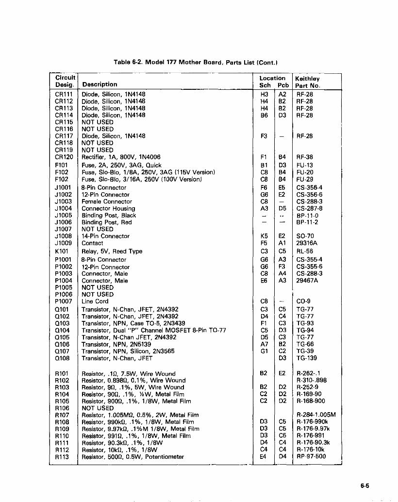
Table 6-2. Model 177 Mother Board. Parts List (Cont.1
Circuil Desig.
CR111 CR1 12 CR113 CR114 CR115 CR1 16 CR117 CR118 CR119 CR120
FlOl F102 F102
JlOOl J1002 J1003 J1004 J1005 J1008 J1007 J1008 J1009 KlOl
PlOOl P1002 P1003 P1004 P1005 P1006 P1007 a101 a102 0103 0104 Q105 Q106 Q107 0108
RlOl R102 R103 R104 R105 R106 R107 RlOB R109 RllO Rlll R112 R113
Description
Diode. Silicon. lN4148 Diode; Silicon; lN4148 Diode, Silicon, lN4148 Diode, Silicon, lN4148 NOT USED NOT USED Diode, Silicon, lN4148 NOT USED NOT USED Rectifier, 1A. BOOV, lN4006
Fuse, 2A. 25OV, 3AG, Quick Fuse, Slo-Blo, l/BA, 25OV. 3AG (115V Version) Fuss, Slo-810, 3/16A, 250V (1OOV VersionJ B-Pin Connector 1ZPin Connsctor Female Connector Connector Housing Binding Post, Black Binding Post, Red NOT USED 14-Pin Connector Contact Relay, 5V. Reed Type
B-Pin Connector 1ZPin Connector Connector, Male Connector, Male NOT USED NOT USED Line Cord Transistor, N-Chan, JFET, 2N4392 Transistor, N-Chan, JFET, 2N4392 Transistor, NPN, Case TO-5, 2N3439 Transistor, Dual “P” Channel MOSFET B-Pin TO-77 Transistor, N-Chan JFET, 2N4392 Transistor, NPN, 2N5139 Transistor, NPN, Silicon, 2N3565 Transistor, N-Chan, JFET
Resistor, .ln, 7.5W, Wire Wound Resistor, 0.898n, 0.1%. Wire Wound Resistor, 90, .l%, 5W, Wire Wound Resistor, 90n. .I %, HW, Metal Film Resistor. 9000, .l%, l/BW, Metal Film NOT USED Resistor, l.O05Ml?, 0.5%, ZW, Meral Film Resistor, SSOkQ, .l %, 1 /BW, Metal Film Resistor, S.S7kn, .l %M l/BW, Metal Film Resistor, 9910, .l%, l/BW, Metal Film Resistor, 90.3kR, ,196. l/BW Resistor, lOkn, .l%, l/BW Resistor. 5000. O.eW, Potentiometer
LOCI Sch H3 H4 H4 B6
F3
Fl
81 C8 C8 F6 G8 CB A3
-
K5 F5 c3
G6 G6 CB E6
C8 c3 D4 Fl c5 D5 A7 Gl
82
82 c2 c2
D3 D3 D3 D4 c4 E4
on Pcb - A2 82 82 03
-
84 D3 84 84 E5 Ez
D5
-
E2 Al
c5 A3 F3 A4 A3
-
c5 c4 c3
Ei 82 c2 D3
E2
D2 D2 D2
c5 c5 c5
E D4
Keithley Part No. RF-28 RF-28 RF-28 RF-28
RF-28
RF-38
FU-13 FU-20 FU-29
(35-3564 CS-356-6 CS-288-3 CS-287-8 BP-11-O BP-11-Z
so-70 29316A RL-56 (35-355-4 CS-355-6 CS-288-3 29467A
co-9 TG-77 TG-77 TG-93 TG-94 TG-77 TG-66 TG-39 TG-139
R-262.. 1 R-310-.898 R-252-9 R-169-90 R-168-900
R-2841.005M R-176-990k R-176.9.37k R-176-991 R-176-90.3k R-176.IOk RP-97-500
65
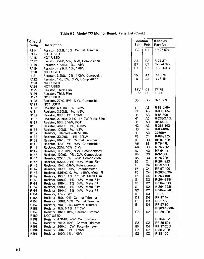
Table 6-2. Model 177 Mother Board, Parts List (Cont.1
Circuit Desig.
R114 R115 R116 R117 R118 Fill9 R120 R121 R122 R123 R124 R125 R126 R127 R128 R129 R130 R131 R132 R133 R134 R135 R136 R137 R138 R139 R140 R141 R142 R143 R144 R145 R146 R147 R148 R149 R150 R151 R152 R153 R154 R155 R156 R157 R158 R159 R160 R161 R162 R163 R184 R165
3escription
3esistor. 50kn, 10%. Cermet Trimmer ‘lOT USED \lOT USED qesistor. 27kQ. 5%. %W. Comoosition 3esistor; 4.32& l’&, 1 ISW qesistor, 4.99k0, 1%. 1/8W UOT USED +.?sistor, 3.9kn. lo%, ll2W. Composition ?esistor, lkR, 5%. SW, Composition UOT USED UOT USED qesistor, Thick Film qesistor, Thick Film UOT USED qesistor. 27kQ. 5%. Yaw. Comoosition UOT UiED qesistor, 6.49kfI. 1%. l/EW qesistor, 3.65kQ, 1 %, l/EW qesistor, 806Q, 1%, 1 IEW ?esistor, 2.15kn, O.l%, l/lOW Metal Film Resistor, 5On, 3/4W. POT Resistor, 4020, 0.1%. 1 I 1OW Resistor, 100kQ. l%, 1/8W Resistor, Selected with VR104 Resistor, 33.2kQ. f 1%. 1/8W Resistor, 50kn. 5%. Cermet Trimmer Resistor, 47kR. 5%. %W, Composition Resistor, 22M, 10%. %W Resistor, lkn, 10%. SW. Potentiometer Resistor, 100kR. I?%, 2W. Composition Resistor, 22kR. 5%, %W, Composition Resistor, 9220, 0.1%. %W, Metal Film Resistor, lOkR, 0.5W. Potentiometer Resistor, 1000, 0.5W. Potentiometer Resistor, 8.95kQ, 0.156, l/lOW. Metal Film Resistor, lOOn, .l%, l/lOW, Metal Film Resistor, 998kR, .l%, ‘/W, Metal Film Resistor, 998kn, .l%, %W, Metal Film Resistor, 998kQ, .l%, %W, Metal Film Resistor, 994kQ. .l%, %W, Metal Film Resistor, Thick Film Resistor, 5kn. 10%. Cermet Trimmer Resistor, 5000. 10%. Cermet Trimmer Resistor, 500, 10%. Cermet Trimmer Resistor, lk0, 0.1%. l/lOW Resistor, 10kQ. 10%. Cermet Trimmer NOT USED Resistor, 4.3MR. I/dW, Composition Resistor, 50kn, lo%,. Cermet Trimmer Resistor, ZOOkfl, .5W. Potentiometer Resistor, 200kR. 1%. 1/8W Resistor, lOOn, l%, 1/8W
I Location Sch Pcb
G2 14 RP-97-6Ok
A7 :2 R-76-27k 87 :3 R-88.4.32k 87 :2 R-88-4.99k
F5 F6
41 R-1.3.9k 41 R-76-l k
SEV SEV
33 TF-79 :3 TF-80
G6 35 R-76.27k
Jl 43 Jl 43 Hl 43 Hl 43 Hl A3 H2 A3 H3 82 Hl A3 F5 c4 Dl D3 A6 !33 A6 83 87 43 85 D3 85 D3 E5 c4 F5 c4 E5 c4 F5 c4 F6 c4 Gl D2 Gl D2 Gl D2 G2 02 Dl 03 Dl 04 El D3 El D4
G2 D2
R-88.6.49k R-88.3.65k R-88-808 R-2632.15k RP-64-50 R-263-402 R-88.100k 27699A R-88.33.2k RP-97.50k R-76.47k R-76.22M RP-64-l k R-3-100k R-76.22k R-264-922 RP-97.10k RP-97-100 R-263.8.95k R-263-100 R-264-998k R-264-998k R-264.998k R-264.994k TF-78 RP-97.5k RP-97-500 RP-97-50 R-263-l .OOOk RP-89.10k
G2 c2 E5 c4 G2 D2 G2 c2
R-76.4.3M RP-89.50k RP-97.200k R-88.200k R-88-100
Keithley Pert No.
6-6
Table 6-2. Model 177 Mother Board, Parts List ICont.1
Circuit Desig.
R166 R167 SlOl 5102 s103 TlOl TlOl UlOl u102 u103 u104 u105 U106 u107 U108 u109 UllO Ulll VRlOl VR102 VRl03 VR104
YlOl
Description
Resistor. 80.6kO. 1%. 1/8W Resistor; lOOk0,‘1%,‘1/8W Switch, Line Selector Switch, Line Battery Switch, 12 Station Pushbutton Transformer, Power (115, 23OV) Transformer, Power 1100, 2OOVl
IC, E-Pin Op-Amp JFET, TL081 IC, BI-FET, Op-Amp, LF351 IC, True RMS-TO-DC Converter, AD536 (TO-100) IC, E-Pin Op-Amp , 741 IC, 4% Digit Analog-Processor, 8052 IC, 4% Digit Logic-Processor, 7103 IC, Linear Op-Amp E-Pin, LM308 IC, J-FET Input Op-Amp, LF355 (selected) IC, Linear Op-Amp E-Pin, LM308 IC, CMOS 14.Stage Binary Converter, 4060 CMOSIMOS Hex Converter, 4089 Regulator, + 5V. 3-Term, TO-220. 7805 Regulator, + 15V. 500mA.78M15 Regulator, -15V. 500mA. 79M15 Regulator, Diode, Selected with R137
Clystal, Quartz fO.Ol%, 1OOkHz
T Location Sch - -
c7 D7 SEV D6 D6
c4 D4 E4 Jl H3 H4 Gl c5 D5 A6 A7 E7 E8 E8
A6
‘cb
A4 B4 E3 A5 A5 c5 c4 05 A2 A2 c2 c2 c3 c3 82 c2 85 85 85
83 -
T Keithley Part No.
R-88.80.6k R-88.100k SW-318 SW-397 294348 TR-168 TR-169
K-196 K-176 IC-172-l IC-42 LSI-12 LSI-11 IC-203 IC-205 IC-203 IC-197 IC-139 IC-93 IC-194 IC-195 27699A
CR-8
6-7
Circuii t Desig. I ET301 c301 C302 c303 c304 c305 CR301 CR302 CR303 CR304 CR305 F301 Q301 Q302 Q303 Q304 0305 0306 Q307 Q308 cl309 Q310 R301 R302 R303 R304 R305 R306 R307 R308 R309 R310 R311 R312 R313 R314 R315 R316 u301 U302
VR301
Table 6-3. Model 1786 Battery Peck, Parts List
Description D Cells for BT301 (4 required)
Capacitor, 4.7/1F, 20V Capacitor, 4.7wF, 20V Capacitor, 1 .OwF, 250V Capacitor, 1OOpF. 35V Capacitor, 1OOpF. 35V Diode, Silicon, lN4148 Diode, Silicon, lN4148 Diode, Silicon, lN4148 Diode, Silicon, lN4148 Diode, Silicon, lN4148
Fuse, 2A, 25OV, 3AG, Quick blow Thyristor, SCR, 106Fl Transistor, NPN, 2N3904 Transistor, PNP, Silicon, TO-92 Case, 2N3905 Transistor, NPN, 2N3904 Transistor, NPN, 2N3904 Transistor, PNP, Silicon, 2N3905 Transistor, NPN, 2N3725 Transistor, NPN, 2N3725 Transistor, PNP, Silicon, MPS-U95 Transistor, PNP, Silicon, TO-92 Case, 2N3905 Resistor, 20kQ. lo%, Cermet Trimmer Resistor, 3300, 10%. ‘/IW. Composition Resistor, lkR, 10%. ‘/4W, Composition Resistor, 3.9kn. 20%. 3W. Wire Wound Resistor, 4.7k0, lo%, %W. Composition Resistor, 3.3kQ. lo%, XW, Composition Resistor, 82I2, 1056, XW, Composition Resistor, 820, 10%. SW, Composition Resistor, lOa, lo%, %W, Composition Resistor, 1On. lo%, %W. Composition Resistor, lOOk0, 1%. l/EW, Composition Resistor, lOOk0, 1%. l/EW, Composition Resistor, lOOkn, 1%. l/EW, Composition Resistor, 6.8M. 10%. 1/4W. Composition Resistor, 578kO. 1%. 1/8W Resistor, 1OOkn. 1%. 1/8W
IC, Dual D-Type Flip-Flop, 4013 IC, l.lV Micro-Power Detector, ICL8211 Regulator, 8.2V. Zener, 1 N785A
I Location Sch I E2
D3 T D4 E4 85 85 83 D4 D4 c5 c5 El
82 B3 D3 03 c4 c4 D3 D4 c2 c2
c3 83 B3 82 84 84 D4 D4 85 El5 D2 D2 D2 D2 D2 D2
c4 D2
83
Pcl
E3 E3 E3 F4 F3 D4 E3 E3 F4 F4
c3 c4 c3 D4 E4 E4 E4 E3 E3 D3 03 c3 c3 D4 D4 D3 c3 E3 E3 F4 F4 E3 E3 E3 E3 E3 E3 D3 E3
:3
Keithley Pert No. BA-33 c-179-4.7 c-179-4.7 C-256-l c-295-100 c-295-100 RF-28 RF-28 RF-28 RF-28 RF-28 FU-13 TG-132 TG-47 TG-53 TG-47 TG-47 TG-53 TG-131 TG-131 TG-133 TG-53 RP-97-20k R-76-330 R-76-lk R-268.3.9k R-76.4.7k R-76.3.3k R-76-82 R-76-82 R-76-10 R-76-10 R-76.100k R-78.100k R-76.100k R-78-6.8M R-88.576k R-88.100k IC-103 IC-177
DZ-61
6-8
DS201 DS202 DS203 DS204 DS205 R201 R202 R203
u201 u202 U203
Table 6-4. Display Board, Parts List
LED, Display, f 1 LED, Display, 7-Segment LED, Display, 7-Segment LED, Dsiplay, 7-Segment LED, Display, 7-Segment Resistor, Thick Film Resistor, Thick Film Resistor, Potentiometer. 2W
IC, CMOS, Quad 2-Input NAND Gate. 4011 IC, Digit Driver, 75492 IC, Segment Driver, 4511
Circuit Desig. Description
C201 I Caoacitor.
A2 E3 E2 E3
-Keithlay Part No.
c-314-4.7 DD-31 DD-30 DD-30 DD-30 DD-30 TF-62 TF-102-3 RP-117.50k
IC-102 IC-169 IC-168
6-9/6-10
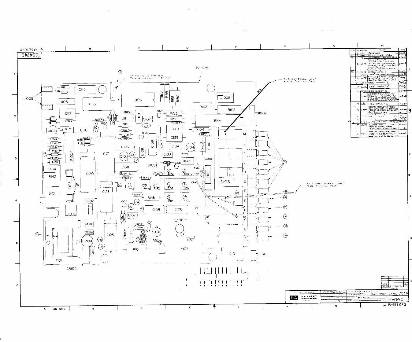
/ JlOO9,>
\
I-
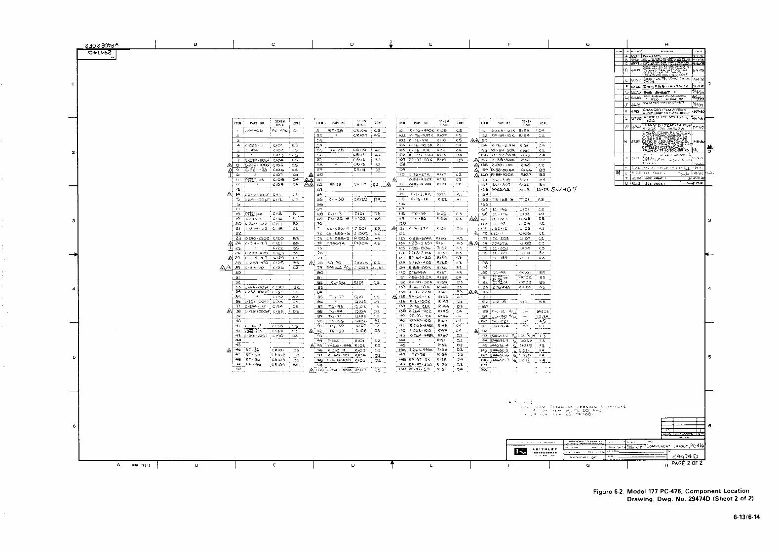
Figure 6.2. Model 177 PC476. Component Location Drawing. Dwg. No. 29474D (Sheet 2 of 2)
6.13/6-14
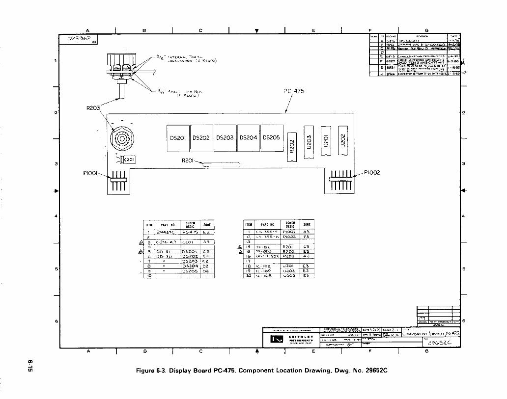
R201, ,
PC;475
/PI002
Figure 83. Display Board PC-475, Component Location Drawing. Dwg. No. 29652C
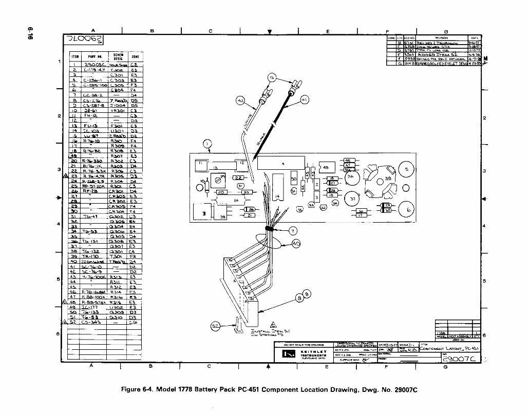
L
Figure 8-4. Model 1778 Battev Pack PC-351 Component Location Drawing, Dwg. No. 29007C
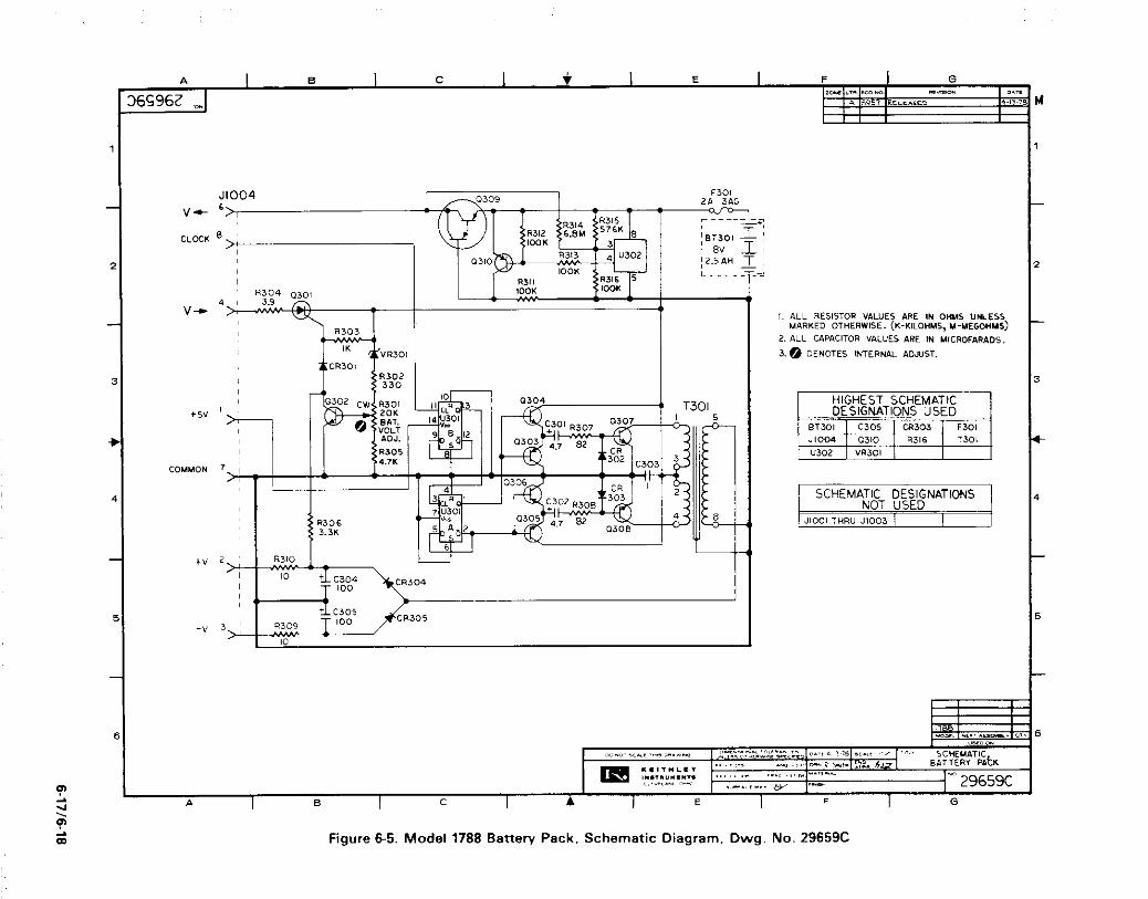
HIGHEST SCHEMATIC DESIGNATIONS USED
BTMl 1 cm5 1 CR303 1 F301 J1004 , 0x0 , R316 1 7301 “302 / “9301 I
Figure 8-5. Model 1788 Batten, Pack. Schematic Diagram. Dwg. No. 29659C
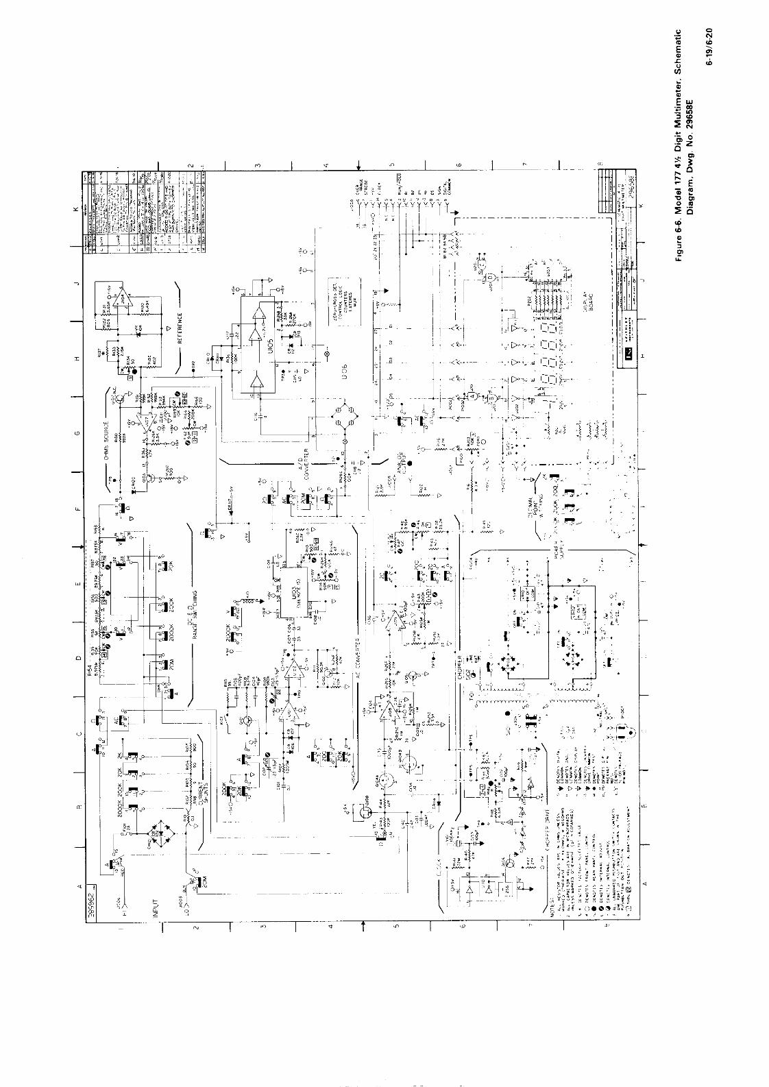
I
II

SERVICE FORM
Model No.
Name
Company
Address
City
Serial No.
State
P.O. No. Date
Phone
-Zip
List all control settings and describe problem. _
~. (Attach additional sheets as necessary.)
Show a block diagram of your measurement system including all instruments connected (whether power is turned on or not). Also describe signal source.
Where is the measurement being performed? (factory, controlled laboratory, out-of-doors, etc.)--~~~
What power line voltage is used? Variation?
Frequency? Ambient Temperature? OF.
Variation? OF. Rel. Humidity? Other?
Any additional information. (If special modifications have been made by the user, please describe below.)
*Be sure to include your name and phone number on this service form