Embed Size (px)
Citation preview

Nanoscale Circuits and Systems Lab
Sameer SonkusaleAssistant Professor, Electrical and Computer Engineering
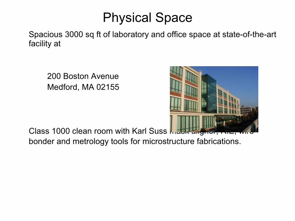
Office: 231A Halligan Hall, 161 College Avenue, MedfordLab: Suite 2700/2850, 200 Boston Ave, Medford
URL: http://nanolab.ee.tufts.edu
Physical SpaceSpacious 3000 sq ft of laboratory and office space at state-of-the-art facility at
200 Boston AvenueMedford, MA 02155
Class 1000 clean room with Karl Suss mask aligner, RIE, wire-bonder and metrology tools for microstructure fabrications.
Where are we located?
200 Boston Ave
To Tufts Main
Starbucks
Office: Halligan Hall
Lab: 200 Boston Ave
Mystic
Valley
Pkwy
Boston Ave
Brown and Brew
Software Facilities• Integrated Circuit Design Environment by Cadence for circuit design,
simulation, layout and verification
• Altium Designer for board level design and layout
• MATLAB for mathematical modeling and simulation
• CODE V from Optical Research Associates for optical simulation
• 3D Electromagnetic Simulation Environment HFSS from ANSOFT
• Agilent EEsof EDA tool for high frequency circuit implementations
• National Instruments LabView Environment for scalable test, measurement and process control applications
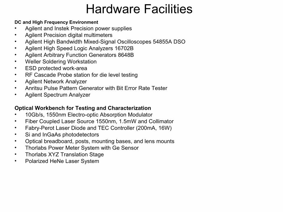
Hardware FacilitiesDC and High Frequency Environment• Agilent and Instek Precision power supplies• Agilent Precision digital multimeters• Agilent High Bandwidth Mixed-Signal Oscilloscopes 54855A DSO• Agilent High Speed Logic Analyzers 16702B• Agilent Arbitrary Function Generators 8648B• Weller Soldering Workstation• ESD protected work-area• RF Cascade Probe station for die level testing• Agilent Network Analyzer • Anritsu Pulse Pattern Generator with Bit Error Rate Tester• Agilent Spectrum Analyzer
Optical Workbench for Testing and Characterization• 10Gb/s, 1550nm Electro-optic Absorption Modulator• Fiber Coupled Laser Source 1550nm, 1.5mW and Collimator• Fabry-Perot Laser Diode and TEC Controller (200mA, 16W)• Si and InGaAs photodetectors• Optical breadboard, posts, mounting bases, and lens mounts• Thorlabs Power Meter System with Ge Sensor• Thorlabs XYZ Translation Stage• Polarized HeNe Laser System
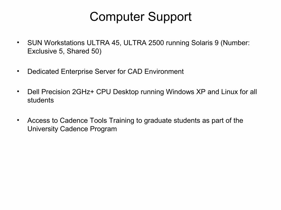
Computer Support
• SUN Workstations ULTRA 45, ULTRA 2500 running Solaris 9 (Number: Exclusive 5, Shared 50)
• Dedicated Enterprise Server for CAD Environment
• Dell Precision 2GHz+ CPU Desktop running Windows XP and Linux for all students
• Access to Cadence Tools Training to graduate students as part of the University Cadence Program
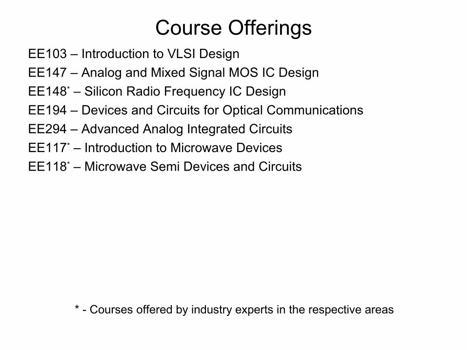
Course OfferingsEE103 – Introduction to VLSI DesignEE147 – Analog and Mixed Signal MOS IC DesignEE148* – Silicon Radio Frequency IC DesignEE194 – Devices and Circuits for Optical CommunicationsEE294 – Advanced Analog Integrated CircuitsEE117* – Introduction to Microwave DevicesEE118* – Microwave Semi Devices and Circuits
* - Courses offered by industry experts in the respective areas
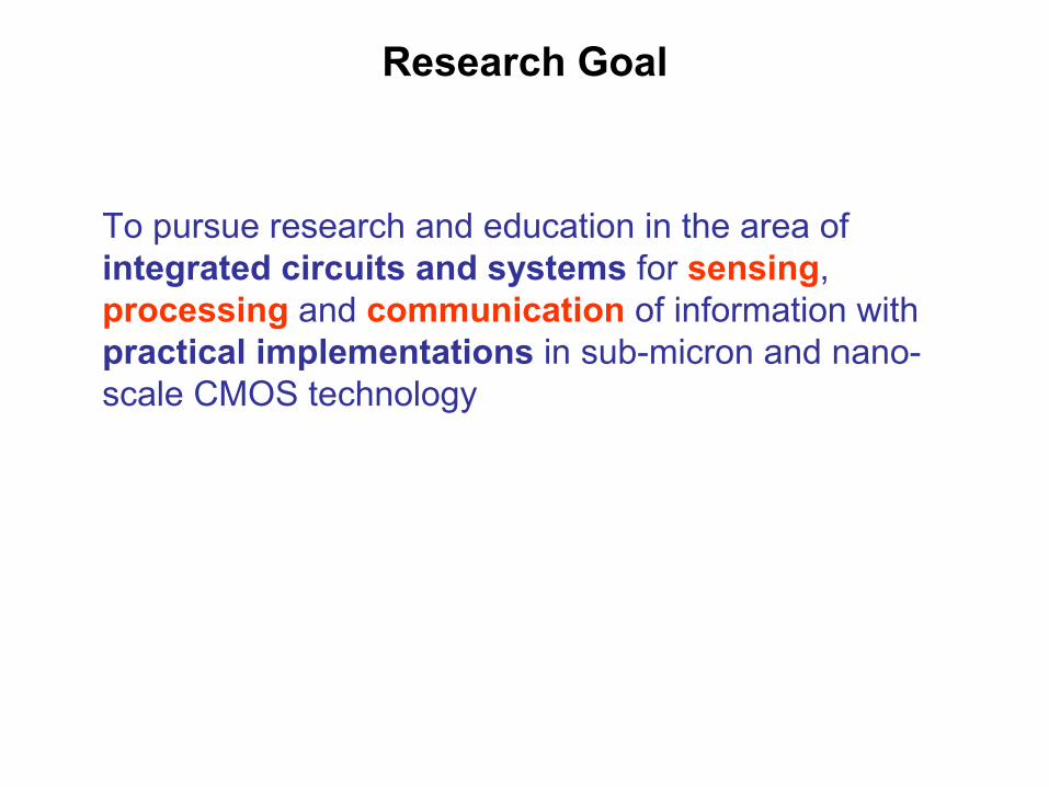
Research Goal
To pursue research and education in the area of integrated circuits and systems for sensing, processing and communication of information with practical implementations in sub-micron and nano-scale CMOS technology
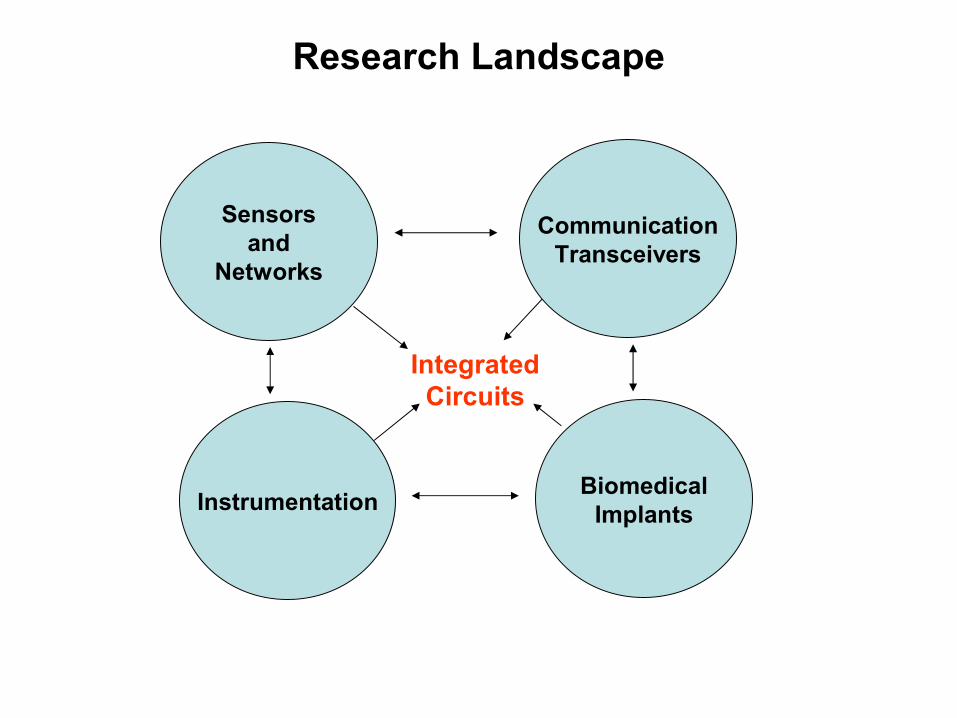
Research Landscape
Sensorsand
Networks
CommunicationTransceivers
Instrumentation BiomedicalImplants
IntegratedCircuits
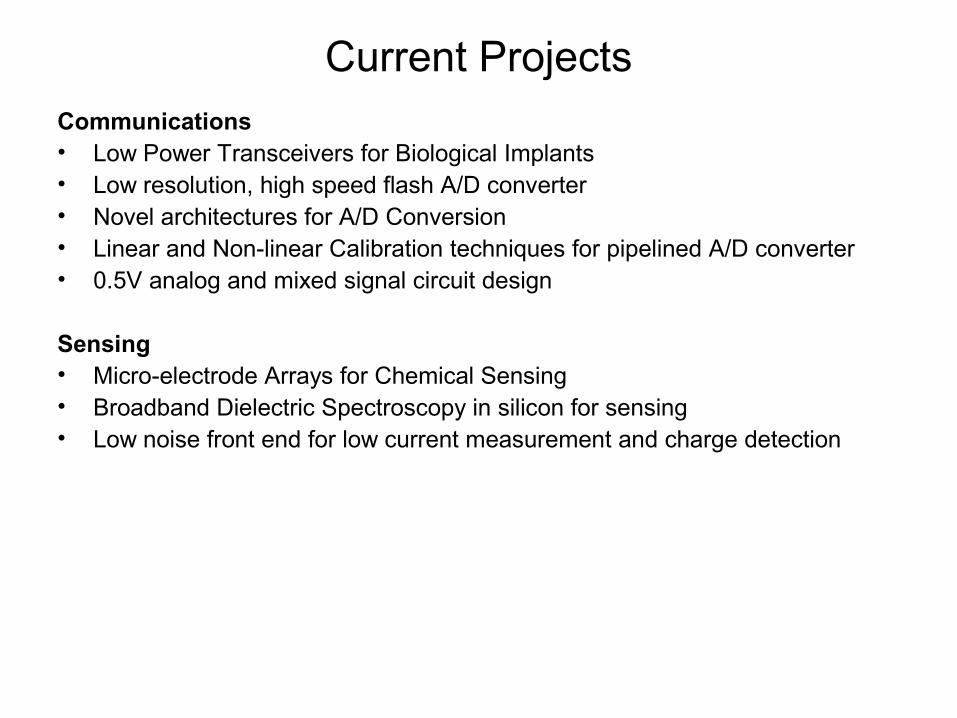
Current ProjectsCommunications• Low Power Transceivers for Biological Implants • Low resolution, high speed flash A/D converter• Novel architectures for A/D Conversion• Linear and Non-linear Calibration techniques for pipelined A/D converter• 0.5V analog and mixed signal circuit design
Sensing• Micro-electrode Arrays for Chemical Sensing• Broadband Dielectric Spectroscopy in silicon for sensing• Low noise front end for low current measurement and charge detection
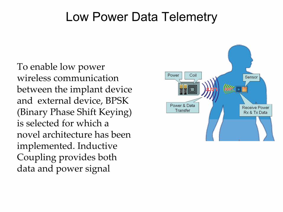
Low Power Data Telemetry
To enable low power wireless communication between the implant device and external device, BPSK (Binary Phase Shift Keying) is selected for which a novel architecture has been implemented. Inductive Coupling provides both data and power signal
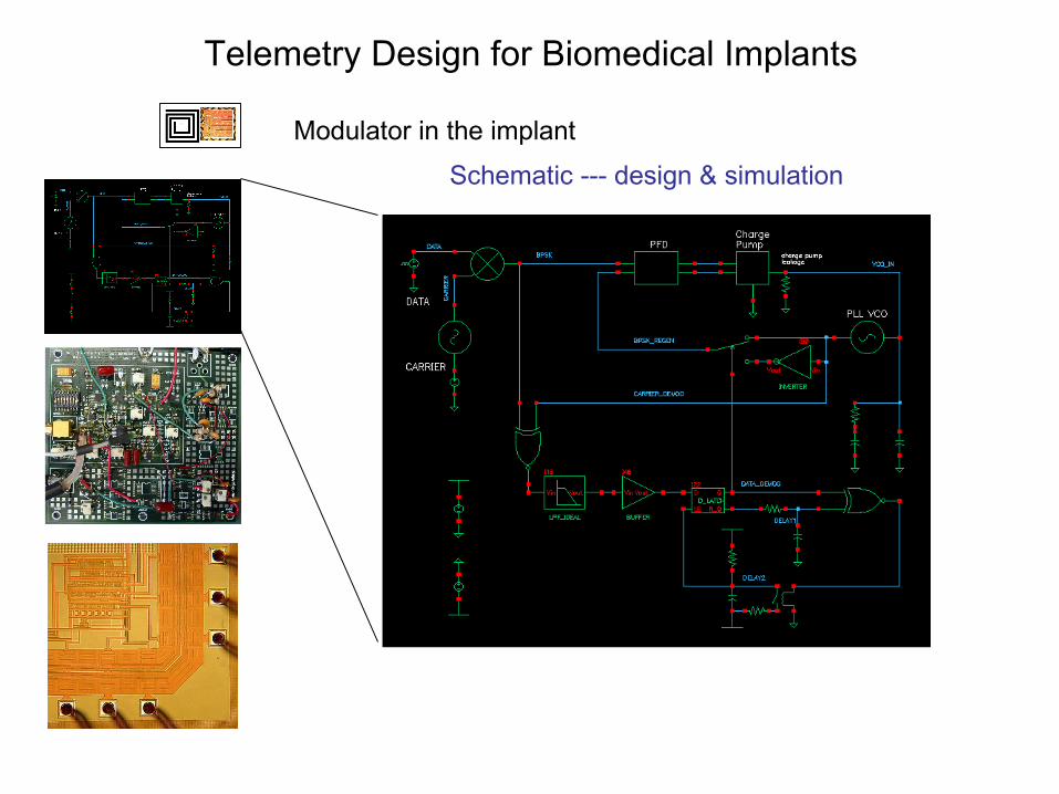
Telemetry Design for Biomedical Implants
Modulator in the implant
Schematic --- design & simulation
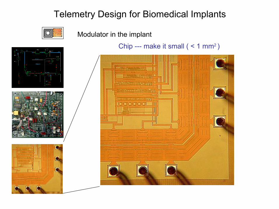
Modulator in the implant
Chip --- make it small ( < 1 mm2 )
Telemetry Design for Biomedical Implants
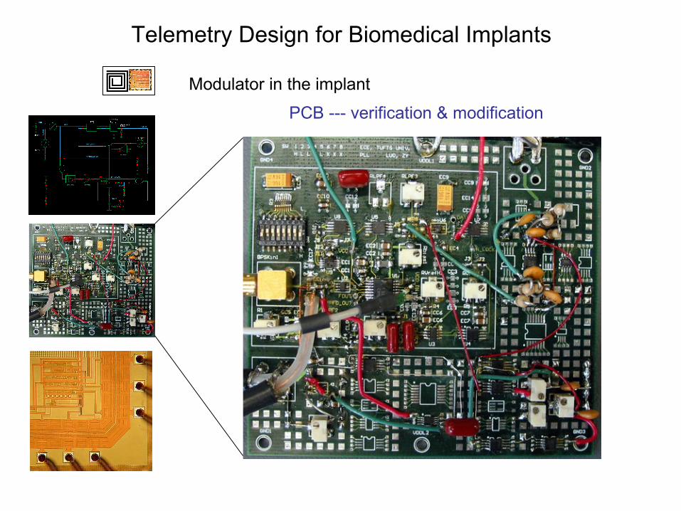
Modulator in the implant
PCB --- verification & modification
Telemetry Design for Biomedical Implants
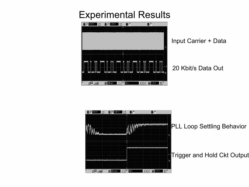
Experimental Results
Input Carrier + Data
20 Kbit/s Data Out
PLL Loop Settling Behavior
Trigger and Hold Ckt Output
Micro-electro-optical Arrays To develop a dense electrode array with on-chip signal
conditioning electronics for electrochemical sensing using various modalities for applications in chemistry, biology and medicine.
– Potentiometric Methods for Sensing– Amperometric Methods for Sensing– Fluorescence Detection
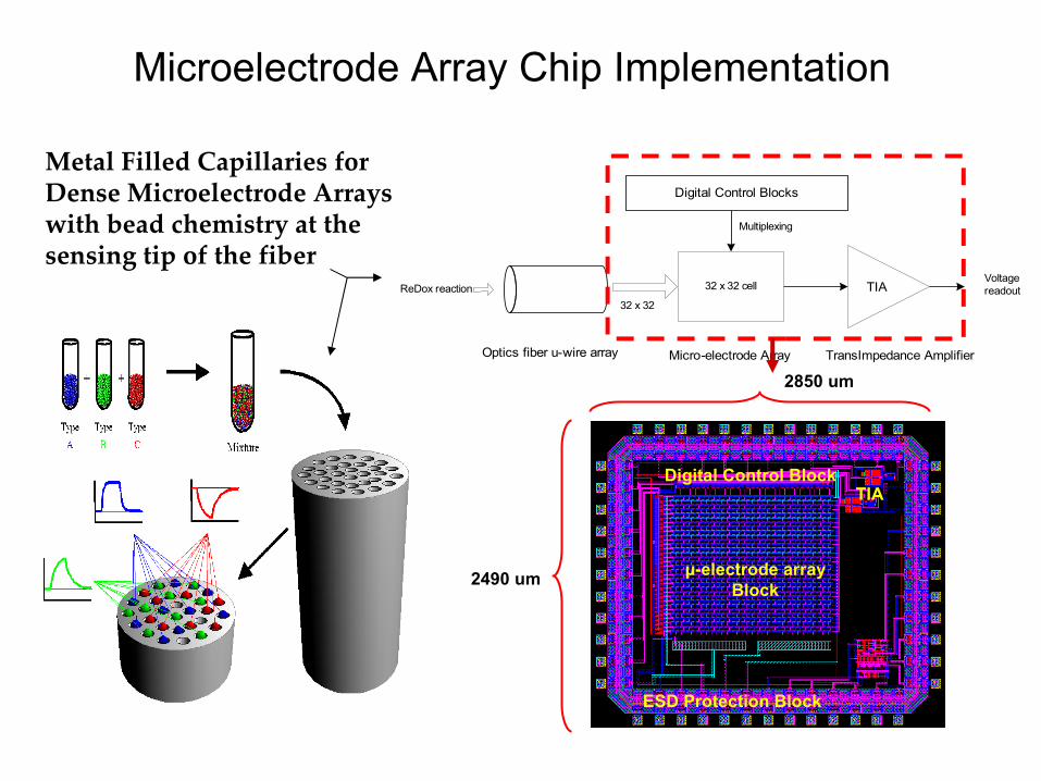
Metal Filled Capillaries forDense Microelectrode Arrays with bead chemistry at the sensing tip of the fiber
32 x 32 cell
TransImpedance AmplifierMicro-electrode Array
Digital Control Blocks
TIA32 x 32
Optics fiber u-wire array
ReDox reactionVoltage readout
Multiplexing
µ-electrode arrayBlock
TIADigital Control Block
ESD Protection Block
2490 um
2850 um
Microelectrode Array Chip Implementation
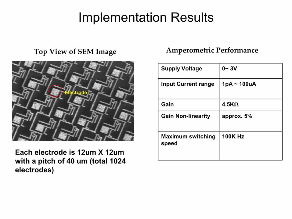
Implementation Results
100K HzMaximum switching speed
approx. 5%Gain Non-linearity
4.5KΩGain
1pA ~ 100uAInput Current range
0~ 3VSupply Voltage
Electrode
Amperometric Performance
Each electrode is 12um X 12um with a pitch of 40 um (total 1024 electrodes)
Top View of SEM Image
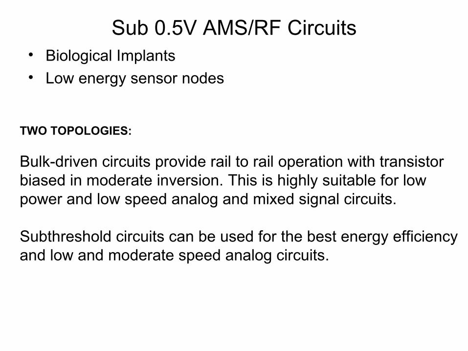
Sub 0.5V AMS/RF Circuits• Biological Implants• Low energy sensor nodes
TWO TOPOLOGIES:
Bulk-driven circuits provide rail to rail operation with transistor biased in moderate inversion. This is highly suitable for low power and low speed analog and mixed signal circuits.
Subthreshold circuits can be used for the best energy efficiency and low and moderate speed analog circuits.
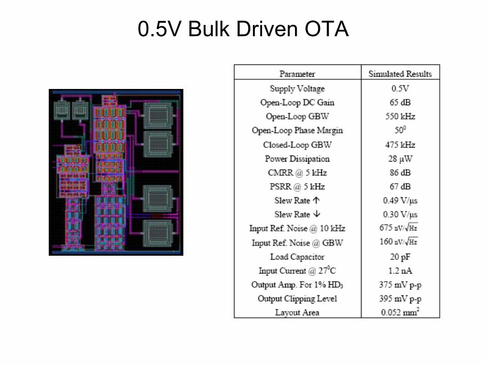
0.5V Bulk Driven OTA
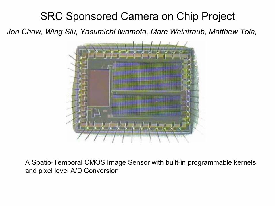
SRC Sponsored Camera on Chip ProjectJon Chow, Wing Siu, Yasumichi Iwamoto, Marc Weintraub, Matthew Toia,
A Spatio-Temporal CMOS Image Sensor with built-in programmable kernelsand pixel level A/D Conversion
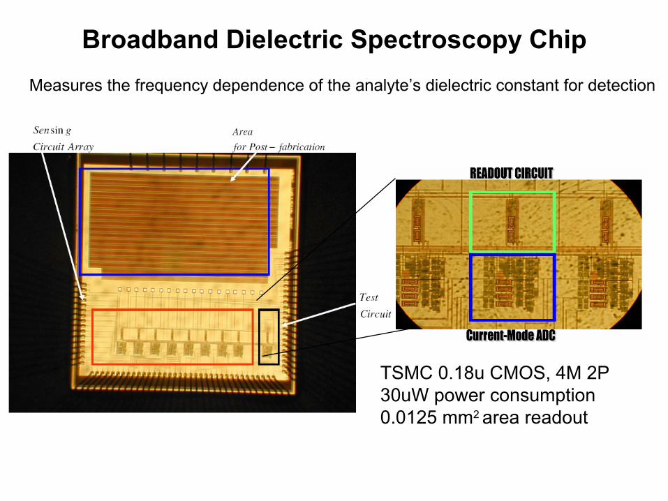
Broadband Dielectric Spectroscopy Chip
TSMC 0.18u CMOS, 4M 2P30uW power consumption0.0125 mm2 area readout
Measures the frequency dependence of the analyte’s dielectric constant for detection
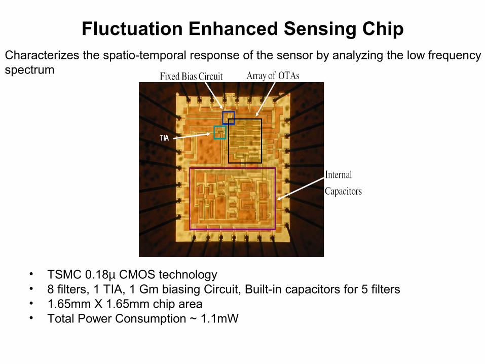
Fluctuation Enhanced Sensing Chip
• TSMC 0.18µ CMOS technology• 8 filters, 1 TIA, 1 Gm biasing Circuit, Built-in capacitors for 5 filters• 1.65mm X 1.65mm chip area• Total Power Consumption ~ 1.1mW
Characterizes the spatio-temporal response of the sensor by analyzing the low frequency spectrum
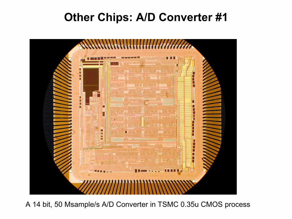
Other Chips: A/D Converter #1
A 14 bit, 50 Msample/s A/D Converter in TSMC 0.35u CMOS process
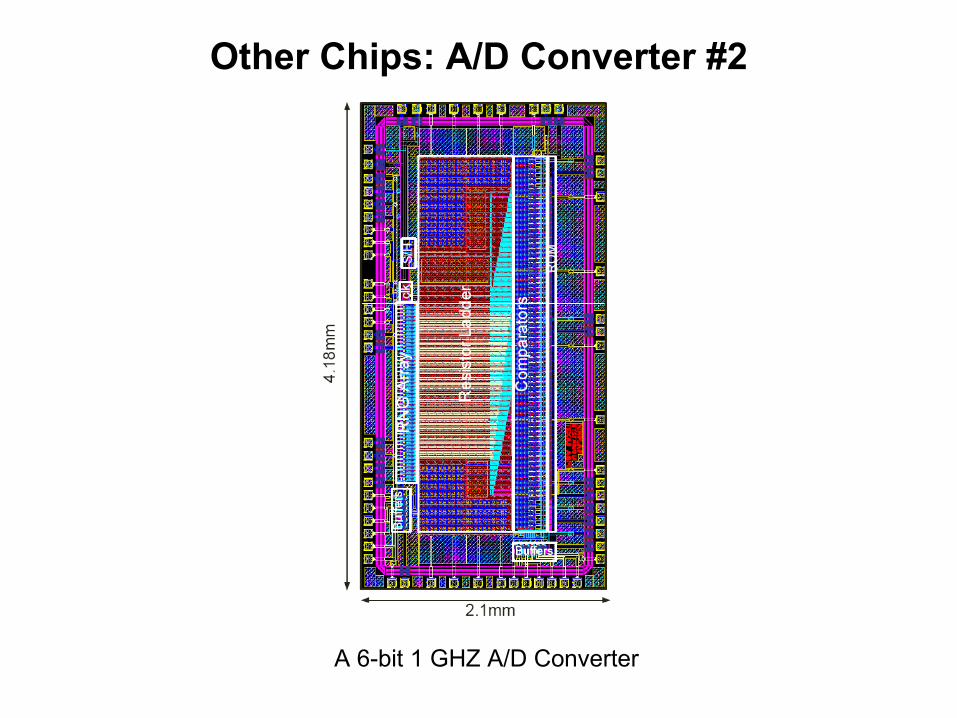
Other Chips: A/D Converter #2
A 6-bit 1 GHZ A/D Converter
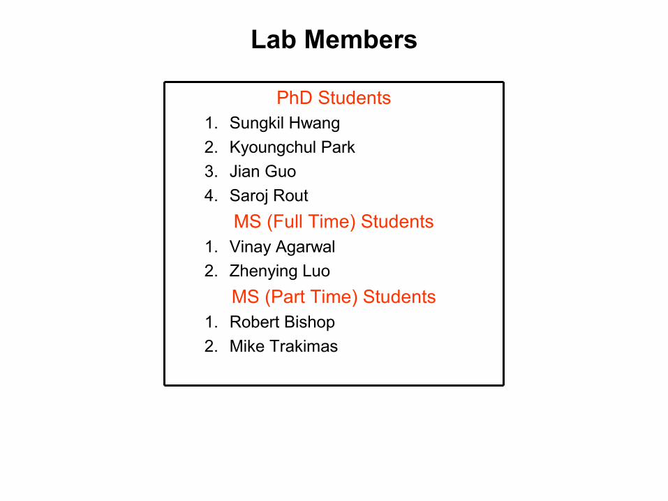
Lab Members
PhD Students1. Sungkil Hwang2. Kyoungchul Park3. Jian Guo4. Saroj Rout
MS (Full Time) Students1. Vinay Agarwal2. Zhenying Luo
MS (Part Time) Students1. Robert Bishop2. Mike Trakimas
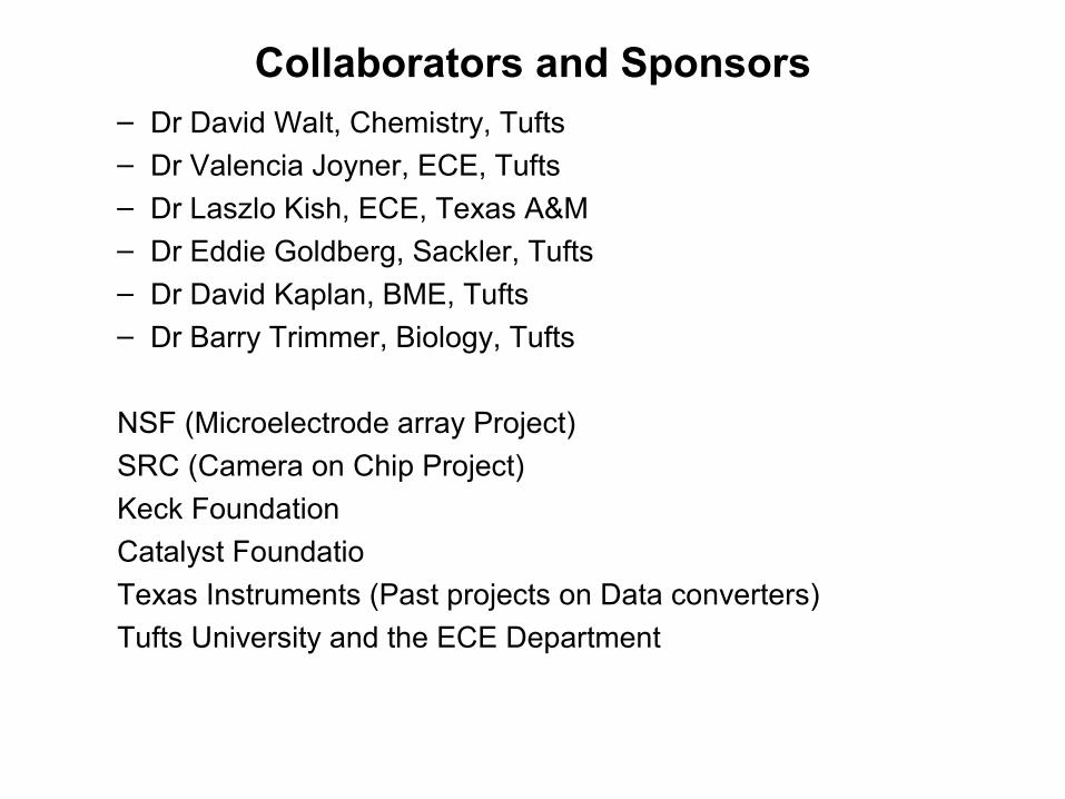
Collaborators and Sponsors– Dr David Walt, Chemistry, Tufts– Dr Valencia Joyner, ECE, Tufts– Dr Laszlo Kish, ECE, Texas A&M– Dr Eddie Goldberg, Sackler, Tufts– Dr David Kaplan, BME, Tufts– Dr Barry Trimmer, Biology, Tufts
NSF (Microelectrode array Project)SRC (Camera on Chip Project)Keck Foundation Catalyst FoundatioTexas Instruments (Past projects on Data converters)Tufts University and the ECE Department