Embed Size (px)
Citation preview
182 PHILlPS TECHNICAL REVIEW VOLUME 27
Integrated circuits with evaporated thin filmsE. C. Munk and A. Rademakers
In this article we shall discuss a form of integratedcircuit in which the conductors, the resistors and thecapacitors (and in some cases the inductors as well) aredeposited as thin films in a pattern of strips and rec-tangles on an insulating substrate. The advantagesusually considered in the integration of circuits havebeen made sufficiently clear in the previous article [11,
and need not therefore be reiterated here.The thin film technique we shall deal with in this
article may be regarded as an extension of the tech-niques in use for making conventional resistors and
539.234 :621.3.049.7
itance or inductance value and the Q that can beachieved with the thin film components may be toolimited.
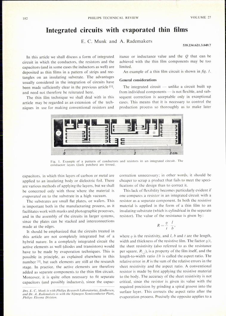
An example of a thin film circuit is shown in jig. J.
General considerations
The integrated circuit - unlike a circuit built upfrom individual components - is not flexible, and sub-sequent correction is acceptable only in exceptionalcases. This means that it is necessary to control theproduction process so thoroughly as to make later
Fig. I. Example of a pattern of conductors and resistors in an integrated circuit. Theconductor layers (dark patches) are tinned.
capacitors, in which thin layers of carbon or metal areapplied to an insulating body or dielectric foil. Thereare various methods of applying the layers, but we shallbe concerned only with those where the material isevaporated on to the substrate in a high vacuum.
The su bstrates are small flat plates, or wafers. Thisis important both in the manufacturing process, as itfacilitates work with masks and photographic processes,and in the assembly of the circuits in larger systems,since the plates can be stacked and interconnectionsmade at the edges.It should be emphasized that the circuits treated in
this article are not completely integrated but of ahybrid nature. In a completely integrated circuit theactive elements as well (diodes and transistors) wouldhave to be made by evaporation techniques. This ispossible in principle, as explained elsewhere in thisnumber [21, but such elements are still at the researchstage. In practice, the active elements are thereforeadded as separate components to the thin film circuit.Moreover, it is quite often necessary to fit separatecapacitors (and possibly inductors), since the capac-
Drs. E. C. Munk is witli Philips Research Laboratories, Eindhoven,and Dr. A. Rademakers is with the Nijmegen Semiconductor Plant,Philips Elcoma Division.
correction unnecessary; in other words, it should becheaper to scrap a product that fails to meet the speci-fications of the design than to correct it.
This lack of flexibility becomes particularly evident ifone compares a resistor in an integrated circuit with aresistor as a separate component. In both the resistivematerial is applied in the form of a thin film to aninsulating substrate (which is cylindrical in the separateresistor). The val ue of the resistance is given by:
e IR=- -
tb'
where e is the resistivity, and I, band t are the length,width and thickness ofthe resistive film. The factor elt,the sheet resistivity (also referred to as the resistanceper square, RO), is a property of the film itself, and thelength-to-width ratio lib is called the aspect ratio. Therelative error in R is the sum of the relative errors in. thesheet resistivity and the aspect ratio. A conventionalresistor is made by first applying the resistive materialto the body. The accuracy of the sheet resistivity is notcritical, since the resistor is given its value with therequired precision by grinding a spiral groove into thesurface layer. This corrects the aspect ratio after theevaporation process. Precisely the opposite applies to a
1966, No. 7 TH1N-FILM INTEGRATED CIRCUITS 183
resistor in a thin film circuit: the dimensions of theresistor are fixed before the film is deposited on thesubstrate. If there are to be no subsequent corrections,the aspect ratio and the sheet resistivity are thereforeestablished independently of one another, which meansthat this must be done with tolerances which togetherdo not exceed the rated tolerance of the resistor. Therequirements for the process of applying ~he resistivelayer are therefore much stricter than in the manufac-ture of separate resistors. These requirements becomeeven harder to meet if the films for the resistors in alarge number of circuits are to be evaporated simul-taneously. The resistive layer must then not only beextremely homogeneous over the entire surface of eachsubstrate, but must also be identical from one substrateto another. These requirements can be met by using theevaporation technique.
The problem can be solved in an entirely different way ifsubsequent individual corrections to the sheet resistivity areallowed. The methods developed by IBM and the Bell Laborator-ies are examples of this approach [3][4]. In both methodsrelatively thick films are used, and the thickness is reduced afterdeposition in the required pattern. In the IBM method theresistive material, in the form of a paste, is screen-printed in therequired pattern upon ceramic wafers. After heat-treatment, theresistance is corrected by sand-blasting. In the second method theresistive material (tantalum with tantalum nitride TaN) is appliedto wafer substrates by sputtering in a gas discharge. After de.position, part of the film is converted by electrolytic oxidationinto non-conducting Ta205. The latter process can now be sowell controlled that a very high accuracy can be achieved. Duringthe process, however, each resistor has to be individually checked.Moreover, optimum properties can only be obtained provided thesheet resistivity is given a relatively Iow value (e.g. 40 Q). Thismeans that resistors with a high nominal value can only beproduced if the aspect ratio has a high value, and this makes itdifficult to meet the requirement for small dimensions.
By way of introduetion to the subject, let us make anestimate of the thicknesses of the films used in thesetechniques. Suppose that we wish to form a combi-nation of resistors with a tolerance of 5%, the highestnominal value among them being 10000 0. Wechoose for this a strip 1 cm long and 100 (.Lmwide.The aspect ratio is then 100 and so the sheet resistivityis 100 0. If we now unsuspectingly put in the bulkresistivity value for say aluminium (2.5 X 10⁻⁸ Om), wearrive at a film thickness of 0.25 nm! The tolerance of5% now has to be shared between the aspect ratio andthe sheet resistivity. This implies that we have toreproduce not only the width of 100 (.Lmbut also thethickness of 0.25 nm with a tolerance certainly below5%. This is scarcely practicable, and it follows thatmaterials of higher resistivity must be used. These areto be found in alloys having resistivities of the order of100 X 10-8 Om. Even with such alloys, the film thick-
nesses are still extremely small, i.e. of the order of10 nm.Various other considerations besides those already
mentioned play a role in the fabrication of evaporatedresistive films. In particular we should mention theefforts to achieve films of low temperature coefficientand high stability: this will be discussed later.If capacitors are to be built up from evaporated thin
films (a dielectric layer between two metal layers)similar considerations indicate the requirements to bemet in the control of the evaporation process, inparticular for the deposition of the dielectric layer. Forthe conductors, the process is of course less critical.
For inductances the thin-film technique is by itsnature not particularly suitable. Without going intodetail, two points may be mentioned in passing: thethree-dimensional character is of more significaneewith the inductor than with other elements, and it isdifficult to concentrate magnetic energy in a smallvolume. For simple requirements, inductors may beevaporated in the form of spirals. In practice thismethod cannot be used for inductances greater than afew tens of (.LHat the most, and to achieve a fairlyreasonable Q the films have to be thickened, e.g. witha layer of gold.
Thin-film effects
Before going further into the production of thin-filmcircuits, we shall first discuss some physical peculiaritiesof thin metal films.The resistance of thin metal films is usually greater
than the value calculated on the basis of the film thick-ness and the resistivity of the metal; in other words the"effective resistivity" of the film is greater than that ofthe bulk metal.An effect of this nature is to be expected in principle
from the theory of electrical conduction in metals. Hereif the thickness of the films becomes smaller than themean free path of the conduction electrons, the scatter-ing of the electrons at the surface will make a percep-tible extra contribution to the resistance. It has in factproved possible to determine fairly accurately the meanfree path from resistance measurements on thin films, atleast for very pure metals in virtually ideal thin films.Ideal films, that is to say films that are continuous,
uniform and homogeneous, are however very rarelyencountered. Usually resistance anomaly in thin films
[1] P. w. Haaijman, Integration of electronic circuits, Philipstech. Rev. 27, 180-181, 1966.
[2] H. C. de Graaff and H. Koelmans, The thin-film transistor,Philips tech. Rev. 27, 200-206, 1966. .
[3] E. M. Davis, W. E. Harding, R. S. Schwartz and J. J. Coming,Solid logic technology: versatile, high-performance micro-electronics, IBM J. Res. DeveI. 8, 102-114, 1964.
[4] D. A. McLean, N. Schwartz and E. D. Tidd, Tantalum-filmtechnology, Proc. IEEE 52, 1450-1462, 1964.
,
184 PHILlPS TECHNICAL REVIEW VOLUME 27
a
c
e
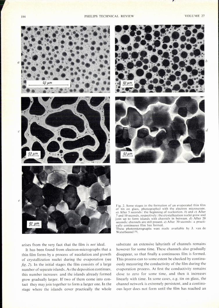
arises from the very fact that the film is not ideal.It has been found from electron-micrographs that a
thin film forms by a process of nucelation and growthof crystallization nuclei during the evaporation (seejig. 2). In the initial stages the film consists of a largenumber of separate islands. As the deposition continues.this number increases and the islands already formedgrow gradually larger. If two of them come into con-tact they may join together to form a larger one. In thestage where the islands cover practically the whole
b
d
Fig. 2. Some stages in the formation of an evaporated thin filmof tin on glass, photographed with the electron microscope.a) After 5 seconds: the beginning of nucleation. b) and c) After7 and 10 seconds, respectively: the crystallization nuclei grow andjoin up to form islands with channels in between. d) After 20seconds: channels are still present. e) After 30 seconds: a practi-cally continuous film has formed.These photomicrographs were made available by J. van deWaterbeemd [5].
substrate an extensive labyrinth of channels remainshowever for some time. These channels also graduallydisappear, so that finally a continuous film is formed.This process can to some extent be checked by continu-ously measuring the conductivity of the film during theevaporation process. At first the conductivity remainsclose to zero for some time, and then it increaseslinearly with time. l n some cases, e.g. tin on glass, thechannel network is extremely persistent, and a continu-ous layer does not form until the film has reached an
1966, No. 7... <.,
THIN-FILM INTEGRATED CIRCq:ITS 185
appreciable thickness, of the order of a few tenths of amicron tsi,A structure may also be formed in other ways. If,
for example, an unbroken, homogeneous thin. film isheated in air, recrystallization takes place in the film.It is possible that oxidation at the grain boundariescauses some electrical separation between the variousdomains.The presence of such structures obviously has con-
siderable influence on the resistance. Quite often elec-trical conduction occurs even before the island systemhas completely closed. How this conduction comesabout is not yet quite clear. It is probable that therm-ionic emission or tunnel processes play some part inthe transport of electrons from one island to another.Where the grain boundaries are oxidized the con-duction must take place through the oxide films.These phenomena have a considerable effect on the
temperature coefficientof resistance. In general, thermalexcitation of the electrons is necessary to (or at leastassists) the kinds of conduction we have referred to, sothat more electrons take part in the conduction as thetemperature increases. This makes a negative contribu-tion to the temperature coefficient. The result is that thetemperature coefficient, which is positive in the bulkmetal (higher resistance at higher temperatures), issmaller for thinner films and in extremely thin filmsmay even be negative.
For practical purposes the thin-film effects are there-fore advantageous in two respects: the effective resist-ivity is greater than in the bulk metal and the temper-ature coefficient is smaller.
Choice of material and evaporation technique
Substrate
The first requirement of a substrate is that it must besufficiently smooth. In order to deposit a film having athickness of the order of 10 nm with adequate precision,the roughness of the substrate surface should at themost be ofthe order of 10 nm. A further requirement isthat the material should be sufficiently heat-resistant,for during the vacuum evaporation process it has to beheated to 250-300 °C to obtain a stable and firmlybonded film. Other requirements that may have to bemet depend on the heat generation in the circuit.Because ofthe miniaturization the dissipation per unitvolume may be substantially greater than in conven-tional circuits. Ifthis results in a high operating temper-ature, the electrical quality must be correspondinglyhigh, so that for example ion transport damage in thesubstrate does not occur. On the other hand, highoperating temperatures can be avoided by measures toensure adequate heat removal. This sets requirements
on the thermal conductivity of the substrate ..Glass is a useful material for this purpose. It ,i~
sufficiently smooth and heat-resistant. A type of glasswith adequate electrical quality must be chosen ~cheapsoda-lime glass, for example, has limitations in thisrespect. above 100 ~c,Normal organic materials areruled out because they are not heat-resistant. Ceramicsare not as a rule smooth enough; even after thoroughlapping they cannot be made much smoother than0.5 [.Lm.Ceramic substrates coated with a thin layer ofglass can, however, be used. If thermal conductivity isimportant, one might consider using ceramics such asporcelain and steatite, which are a few times better thanglass in this respect. Sintered AhOa or sintered-Beï),whose thermal conductivities are about ten and ahundred times betterthan glass respectively, could alsobe employed.
Resistors
We shall now consider the resistivefilms in somewhatmore detail, confining ourselves to a type made byPhilips. The starting material is a nickel-chromium alloy.In wire form and with the composit!.pn 80% Ni, ,10%Cr, this has a resistivity of roughly 100 X .10-8 Qm. Dueto oxidation and the thin-film effectsmentioned above,the effective resistivity in the vacuum-deposited form isconsiderably higher. say 400 X 10-8 Qm: Moreover; ifthe composition is suitably chosen" the températurecoefficient of NiCr is small.NiCr has two further important properties that
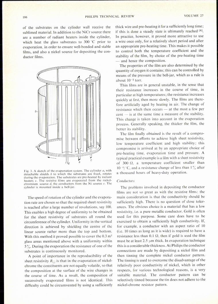
strongly indicate the choice of this material. FirstIy, itadheres well to glass, - clearly an important feature.Secondly, the material begins to evaporate quite rapidlyat temperatures below the melting point. This meansthat a solid source can be used for evaporation. A linearsource can therefore be used, and this is of considerableadvantage in the uniform coating oflarge areas. This ismuch more difficult if the source is a molten metal. 'The vacuum-evaporation equipment, which is
completely contained in a bell-jar, is illustrated infig. 3.The substrates are fixed to the inside of a cylinder whichrotates at a uniform speed around its axis during theevaporation. Inside the cylinder, parallel with its axis,is a linear NiCr' source in the form of a wire or strip,which is heated by an electric current to a temperaturejust below the melting point. The extent of the sourceallows a reasonable rate of deposition. For instance,with an 80 cm nickel-chromium wire of 2mm diameteras the source, a film of sheet resistivity RO = 300 Q canbe deposited on an area of 0.3 m2 in 10 minutes. Thesource is partly screened, so that only a few at a time
[5] J. van de Waterbeemd, Philips Res. Repts. 21, 27-48, 1966,(No. I).
186 PHJLIPS TECHNICAL REVIEW VOLUME 27
of the substrates on the cylinder wall receive thesublimed material. In addition to the NiCr source thereare a number of radiant heaters inside the cylinder,which heat the glass substrates to 300°C prior toevaporation, in order to ensure well-bonded and stablefilms, and also a nickel source for depositing the con-ductor films.
b
c ~
..------... ,n~,- "-TI .) L ,~
I
~
, I
i
11
I'
-I1
Iilllil= -cr 'Q,( I~v- 1----- v11~ v~a
uc
Fig. 3. A sketch of the evaporation system. The cylinder a, withdetachable shields b to which the substrates are fixed, rotatesduring the evaporation. The substrates are pre-heated by radiantheaters c. The resistive films are evaporated from the nickeI-chromium source d, the conductors from the Ni source e. Thecylinder is mounted inside a bell-jar.
The speed of rotation of the cyl inder and the evapora-tion rate are chosen so that the required sheet resistivityis reached after a large number of revolutions, say 100.This enables a high degree ofuniformity to be obtainedfor the sheet resistivity of substrates all round thecircumference ofthe cylinder. Uniformity in the verticaldirection is achieved by shielding the centre of thelinear source rather more than the top and bottom.With this method it proved possible to cover the 0.3 m2
glass areas mentioned above with a uniformity within5%. During the evaporation the resistance of one ofthesubstrates is continuously monitored.
A point of importance in the reproducibility of thesheet resistivity RO is that in the evaporation of nickel-chrome the constituents are not equally volatile, so thatthe composition at the surface of the wire changes inthe course of time. As a result, the composition ofsuccessively evaporated films is not identical. Thisdifficulty could be circumvented by using a sufficiently
thick wire and pre-heating it for a sufficiently long time;if this is done a steady state is ultimately reached [6l.
In practice, however, it proved more attractive to usea wire once only, for a relatively short period and afteran appropriate pre-heating time. This makes it possibleto control both the temperature coefficient and thestability of the film, by choice of the pre-heating time- and hence the composition.
The properties of the film are also determined by thequantity of oxygen it contains; this can be controlled bymeans of the pressure in the bell-jar, which as a rule isabout 10-5 torr .
Thin films are in general unstable, in the sense thattheir resistance increases in the course of time, inparticular at high temperatures; the resistance increasesquickly at first, then more slowly. The films are there-fore artificially aged by heating in air. The change ofresistance which then occurs - at the most a few percent - is at the same time a measure of the stability.This change is taken into account in the evaporationprocess. Generally speaking, the thicker the film, thebetter its stability.
The film finally obtained is the result of a compro-mise between efforts to achieve high sheet resistivity,low temperature coefficient and high stability; thiscompromise is arrived at by an appropriate choice ofpre-heating time, evaporation time and pressure. Atypical practical example is a film with a sheet resistivityof 300 Q, a temperature coefficient smaller thanIO-4;oC, and a resistance change of less than I % aftera thousand hours of heavy-duty operation.
Conductors
The problems involved in depositing the conductorfilms are not so great as with the resistive films: themain consideration is that the conductivity should besufficiently high. There is no question of close toler-ances. The obvious choice is a material that has a lowresistivity, i.e. a pure metallic conductor. Gold is oftenused for this purpose. Some care does have to beexercised to obtain a sufficiently high conductivity. If,for example, a conductor with an aspect ratio of 10(i.e. 10 times as long as it is wide) is required to have aresistance less than 0.1 Q, then if gold is used the filmmust be at least 2.5 [.Lmthick. In evaporation techniquethis is a considerable thickness. At Philips the conductorconnections are made by depositing a nickel film andthen tinning the complete nickel conductor pattern.The tinning is used to overcome the disadvantage oftherelatively poor conductivity of nickel, which in otherrespects, for various technological reasons, is a verysuitable material. The conductor pattern can beselectively tinned because the tin does not adhere to thenickel-chrome resistor pattern.
1966, No. 7 THIN-FILM INTEGRATED CIRCUiTS 187
Dielectrics
Dielectric films as well can be deposited as the di-electrics for the capacitors in the circuit. The object isto obtain the highest possible capacitance per unit areawhile ensuring that the breakdown voltage remains at asafe margin above the working voltage. Low dielectriclosses and not too high a temperature coefficient arealso desirable.
The film that has been most investigated and used isa silicon oxide film produced by evaporating siliconmonoxide. The cornposition of the film again dependson what exactly happens in the vacuum during evapora-tion. It is certain that there is more oxygen present inthe deposited film than indicated by the formula SiO.A safe field-strength for films of this kind is 10 VIfLm.At an operating voltage of a few volts the minimumthickness must then be 0.5-1 fi.m, which, for Sr = 4to 5, gives a capacitance of 40 to 80 pF per mmê.
Dielectric films are much more sensitive to imperfec-tions than resistive films. If there is a hole in the di-electric film, the result will be a short-circuit when thenext electrode is deposited, whereas in the resistive filmthe current would simply flow around the hole. It istherefore particularly important to avoid dust whenmaking dielectric films. Experience has shown that thechance of short-circuiting increases sharply with thesize of the surface. In practice the capacitances used arelimited to a few thousand pF.
Various ways of increasing the capacitance per unitarea have been tried, so far without conspicuoussuccess. One is to use much thinner dielectric layerssuch as those found in the electrolytic capacitor. This isdone for example by evaporating tantalum, anodicallyoxidizing it and then, after it has been dried, evaporat-ing an upper electrode on to it r41. By this method1000 pF/mm2 can be achieved for voltages of the sameorder as mentioned above (5 to 10 V). As yet, however,reasonably reliable capacitors have been made by thismethod on only a modest scale. Much less progress hasbeen made in efforts to deposit materials that have arelatively high dielectric constant, such as Ti02 andBaTi03.It has proved to be a practical proposition to use thin
ceramic wafers ofthe latter materials (e.g. 0.1 mm thick)which have been provided with evaporated electrodes.If these are soldered flat in the circuit they take up littlespace, and the existing choice of materials and thick-nesses makes it possible to achieve capacitances up to200 pF/mm2.
Generating the pattern
In addition to the problem of producing films withspecific properties there is also the problem of how to
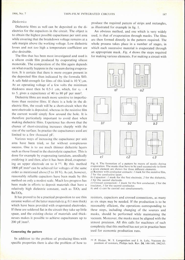
produce the required pattern of strips and rectangles,as illustrated for example in fig. I.An obvious method, and one which is very widely
used, is that of evaporation through masks. The filmsare then formed directly in the pattern required. Thewhole process takes place in a number of stages, inwhich each successive material is evaporated throughan appropriate mask. Fig. 4 shows the steps requiredfor making various elements. For making a circuit with
a7
"----,I II I
"'---,f" J:I;):~'; I
r-g. '1+--'h-l
I II IJ JJ JI. .I --- .•••• '('L_,,,t,: -- _ ....J
r _.J L_-,
I II II II II IL J
b7 b2 b3
Fig. 4. The formation of a pattern by means of masks duringevaporation. The masks that have to be used successively to forma given element are shown for three different elements.a) Resistor with conductor contacts: } mask for the resistive film,2 for the conductive layer.bl Capacitor: I mask for the first electrode, 2 for the dielectric,3 for the second electrode.cl Crossed connection: 1 mask for the first conductor, 2 for theinsulator, 3 for the second conductor.bl and c) can be carried out simultaneously.
resistors, capacitors and crossed connections, as manyas six steps may be needed. If the production is to bereasonably efficient, the operations corresponding tothese steps, including changing of the sources andmasks, should be performed while maintaining thevacuum. Moreover, the masks must be aligned with theutmost precision. All this calls for machines of suchcomplexity that this method has not yet in practice beenused for economic production runs.
[6.] P. Huijer, W. T. Langendam and J. A. Lely, Vacuum de-position of resistors, Philips tech. Rev. 24, 144-149, 1962/63.
188 PHILlPS TECHNICAL REVIEW VOLUME 27
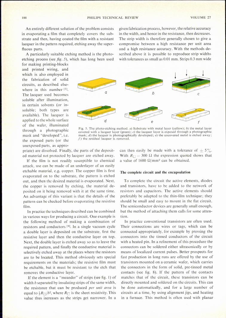
Fig. 5. The photo-etching method. a) Substrate with metal layer (yellow); b) the metal layercovered with a lacquer layer (green); c) the lacquer layer is exposed through a photographicmask; d) the lacquer is photographically developed; e) the uncovered metal is etched away;f) the residual lacquer is removed.
An entirely different solution of the problem consistsin evaporating a film that completely covers the sub-strate and then, having coated the film with a resistantlacquer in the pattern required, etching away the super-fluous parts.
A particularly suitable etching method is the photo-etching process (see fig. 5), which has long been usedfor making printing-blocksand printed wiring, andwhich is also employed inthe fabrication of solidcircuits, as described else-where in this number [71.
The lacquer used becomessolu bie after illumination,in certain solvents (or in-soluble; both types areavailable). The lacquer isapplied to the whole surfaceof the wafer, illuminatedthrough a photographicmask and "developed", i.e.the exposed parts (or theunexposed parts, as appro-priate) are dissolved. Finally, the parts of the deposit-ed material not protected by lacquer are etched away.If the film is not readily susceptible to chemical
attack, use can be made of an underlayer of an easilyetchable material, e.g. copper. The copper film is firstevaporated on to the substrate, the pattern is etchedout, and then the desired material is evaporated. Next,the copper is removed by etching, the material de-posited on it being removed with it at the same time.An advantage of this variant is that the details of thepattern can be checked before evaporating the resistivefilm.
In practice the techniques described can be combinedin various ways for producing a circuit. One example isthe following method of making a combination ofresistors and conductors [81. In a single vacuum cyclea double layer is deposited on the substrate, first theresistive layer and then the conductive layer on top.Next, the double layer is etched away so as to leave therequired pattern, and finally the conductive material isselectively etched away at the places where the resistorsare to be located. This method obviously sets specialrequirements on the materials; the resistive film mustbe etchable, but it must be resistant to the etch thatremoves the conductive layer.
If the element is a "meander" of strips (see fig. 1) ofwidth b separated by insulating strips ofthe same width,the resistance that can be produced per unit area isequal to tRofb2, where RO is the sheet resistivity. Thisvalue thus increases as the strips get narrower. In a
given fabrication process, however, the relative accuracyin the width, and hence in the resistance, then decreases.The strip width is therefore generally chosen to give acompromise between a high resistance per unit areaand a high resistance accuracy. With the methods de-scribed above it is possible to reproduce strip widthswith tolerances as small as 0.01 mm. Strips 0.3 mm wide
~/1'/ /h /H .....<>:::•.
e
can then easily be made with a tolerance of ± 5%.With Ro = 300 D the expression quoted shows thata value of 1600 Dfmm2 can be obtained.
The complete circuit and the encapsulation
To complete the circuit the active elements, diodesand transistors, have to be added to the network ofresistors and capacitors. The active elements shouldpreferably be adapted to the thin-film technique; theyshould be small and easy to mount in the flat circuit.The semiconductor devices are generally small enough,but the method of attaching them calls for some atten-tion.
In practice conventional transistors are often used.Their connections are wires or tags, which can beconnected appropriately, for example by pressing theconnectors into the tinned conductors of the circuitwith a heated pin. In a refinement of this procedure theconnectors can be soldered either ultrasonically or bymeans of localized current pulses. Better prospects forfast production in long runs are offered by the use oftransistors mounted on a ceramic wafer, which carriesthe connectors in the form of solid, pre-tinried metalcontacts (see fig. 8). If the pattern of the contactsmatches that of the circuit, these transistors can bedirectly mounted and soldered on the circuits. This canbe done automatically, and for a large number ofcircuits at a time, by using alignment jigs, and heatingin a furnace. This method is often used with planar
1966, No. 7 THIN-FILM INTEGRATED CIRCUITS 189
silicon transistors. In a promising variant of thesetransistors the ceramic wafer is completely dispensedwith, and the silicon crystal is soldered directly into thecircuit. The crystals, which are about 0.6 X 0.6 mm, arepre-coated with an extremely thin layer of glass. Thecontacts are minute tinned beads mounted in smallholes in the glass film [9l.
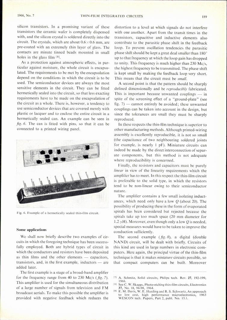
As a proteetion against atmospheric effects, in par-ticular against moisture, the whole circuit is encapsu-lated. The requirements to be met by the encapsulationdepend on the conditions in which the circuit is to beused. The semiconductor devices are always the mostsensitive elements in the circuit. They can be fittedhermetically sealed into the circuit, so that less exactingrequirements have to be made on the encapsulation ofthe circuit as a whole. There is, however, a tendency touse semiconductor devices that are covered merely withplastic or lacquer and to enclose the entire circuit in aherrnetically sealed can. An example can be seen injig.6. The can is fitted with pins, so that it can beconnected to a printed wiring panel.
Fig. 6. Example of a hermetically sealed thin-film circuit.
Some applications
We shall now briefly describe two examples of cir-cuits in which the foregoing technique has been success-fully employed. Both are hybrid types of circuit inwhich the conductors and resistors have been depositedas thin films and the other elements - capacitors,transistors, and, in the first example, inductors - areadded later.
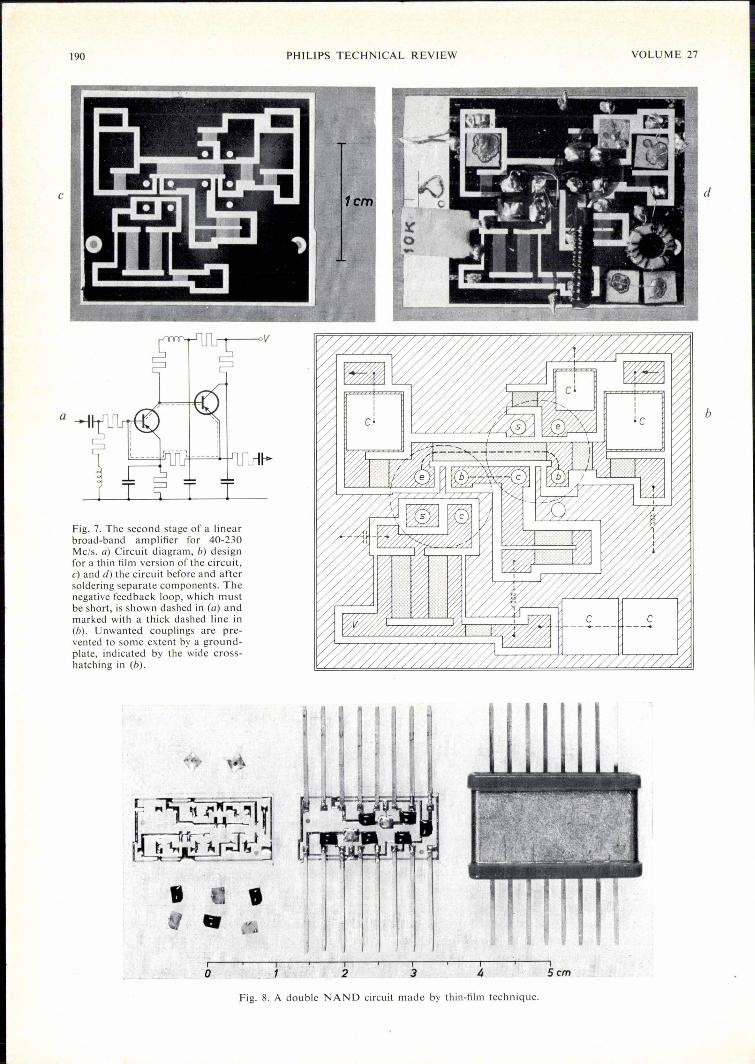
The first example is a stage of a broad-band amplifierfor the frequency range from 40 to 230 Mc/s (jig. 7).This amplifier is used for the simultaneous distributionof a large number of signals from television and FMbroadcast aerials. To make this possible the amplifier isprovided with negative feedback which reduces the
distortion to a level at which signals do not interferewith one another. Apart from the transit times in thetransistors, capacitive and inductive elements alsocontribute to the parasitic phase shift in the feedbackloop. To prevent oscillation tendencies the parasiticphase shift should be kept a great deal smaller than 1800
up to that frequency at which the loop gain has droppedto unity. This frequency is much higher than 230 Mc/s,the highest frequency to be transmitted. The phase shiftis kept small by making the feedback loop very short.This means that the circuit must be small.
A second point is that the pattern should be sharplydefined dimensionally and be reproducibly fabricated.This is important because unwanted couplings - inspite of the screening effect of a "ground-plate" (seefig. 7) - cannot entirely be avoided; these unwantedcouplings can be taken into account in the design, butsince the tolerances are small they must be sharplyreproduced.
In these respects the thin-film technique is superior toother manufacturing methods. Although printed-wiringassembly is excellently reproducible, it is not so small(the capacitance of two neighbouring soldered jointsfor example, is nearly I pF). Miniature circuits canindeed be made by the direct interconnection of separ-ate components, but this method is not adequatewhere reproduci bility is concerned.
Finally, the resistors and capacitors must be purelylinear in view of the linearity requirements which theamplifier has to meet. In this respect the thin-film circuitis preferable to the solid type, in which the resistorstend to be non-linear owing to their semiconductornature.
The amplifier contains a few small isolating induct-ances, which need only have a low Q (about 20). Thepossibility of producing these in the form of evaporatedspirals has been considered but rejected because thespirals take up too much space (20 mm diameter for1.2 fI.H).Moreover, even though only a low Q is needed,special measures would have to be taken to improve theconduction sufficiently.
The second example (jig.8), a digital (doubleNAND) circuit, will be dealt with briefly. Circuits ofthis kind are used in large numbers in electronic com-puters. Here again, the principal virtue of the thin-filmtechnique is that it makes miniature circuits possible, sothat compact computers can be built. Moreover
[7] A. Schmitz, Solid circuits, Philips tech. Rev. 27, 192-199,1966.
[8] See C. W. Skaggs, Photo-etching thin-film circuits, Electronics37, No. 18, 94-98, 1964.
[9] E. M. Davis, W. E. Harding and R. S. Schwartz, An approachto low cost, high performance microelectronics, 1963WESCON tech. Papers, Part 2, publ. No. 13.1.
I I •• 'u
0 _,1y
2~. 3 .4
190
c
Fig, 7. The second stage of a linearbroad-band amplifier for 40-230Mc/s. a) Circuit diagram, b) designfor a thin film version of the circuit,c) and d) the circuit before and aftersoldering separate components. Thenegative feedback loop, which mustbe short, is shown dashed in (a) andmarked with a thick dashed line in(b). Unwanted couplings are pre-vented to some extent by a ground-plate, indicated by the wide cross-hatching in (b).
PHILIPS TECHNICAL REVIEW VOLUME 27
d
b
Fig. 8. A double NAND circuit made by thin-film technique.
5cm
1966, No. 7 THIN-FILM INTEGRATED CIRCUITS 191
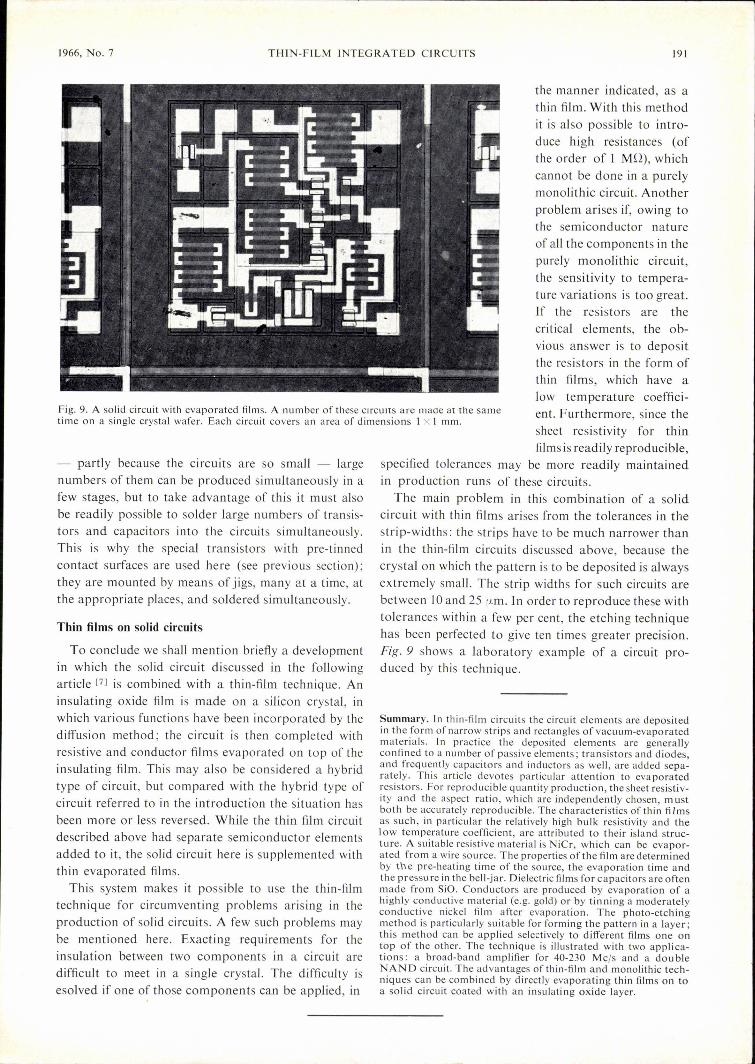
Fig. 9. A solid circuit with evaporated films. A number of these Circuits are made at the sametime on a single crystal wafer. Each circuit covers an area of dimensions 1 X I mm.
- partly because the circuits are so small - largenumbers of them can be produced simultaneously in afew stages, but to take advantage of this it must alsobe readily possible to solder large numbers of transis-tors and capacitors into the circuits simultaneously.This is why the special transistors with pre-tinnedcontact surfaces are used here (see previous section);they are mounted by means of jigs, many at a time, atthe appropriate places, and soldered simultaneously.
Thin films on solid circuits
To conclude we shall mention briefly a developmentin which the solid circuit discussed in the followingarticle [7] is combined with a thin-film technique. Aninsulating oxide film is made on a silicon crystal, inwhich various functions have been incorporated by thediffusion method; the circuit is then completed withresistive and conductor films evaporated on top of theinsulating film. This mayalso be considered a hybridtype of circuit, but compared with the hybrid type ofcircuit referred to in the introduetion the situation hasbeen more or less reversed. While the thin film circuitdescribed above had separate semiconductor elementsadded to it, the solid circuit here is supplemented withthin evaporated films.
This system makes it possible to use the thin-filmtechnique for circumventing problems arising in theproduction of solid circuits. A few such problems maybe mentioned here. Exacting requirements for theinsulation between two components in a circuit aredifficult to meet in a single crystal. The difficulty isesolved if one of those components can be applied, in
the manner indicated, as athin film. With this methodit is also possible to intro-duce high resistances (ofthe order of 1 MD), whichcannot be done in a purelymonolithic circuit. Anotherproblem arises if, owing tothe semiconductor natureof all the components in thepurely monolithic circuit,the sensitivity to tempera-ture variations is too great.If the resistors are thecritical elements, the ob-vious answer is to depositthe resistors in the form ofthin films, which have alow temperature coeffici-ent. Furthermore, since thesheet resistivity for thinfilms is readily reproducible,
specified tolerances may be more readily maintainedin production runs of these circuits.
The main problem in this combination of a solidcircuit with thin films arises from the tolerances in thestrip-widths: the strips have to be much narrower thanin the thin-film circuits discussed above, because thecrystal on which the pattern is to be deposited is alwaysextremely small. The strip widths for such circuits arebetween 10 and 25 (J.m.In order to reproduce these withtolerances within a few per cent, the etching techniq uehas been perfected to give ten times greater precision.Fig. 9 shows a laboratory example of a circuit pro-duced by this technique.
Summary. In thin-film circuits the circuit elements are depositedin the form of narrow strips and rectangles of vacuum-evaporatedmaterials. In practice the deposited elements are generallyconfined to a number of passive elements; transistors and diodes,and frequently capacitors and inductors as well, are added sepa-rately. This article devotes particular attention to evaporatedresistors. For reproducible quantity production, the sheet resistiv-ity and the aspect ratio, which are independently chosen, mustboth be accurately reproducible. The characteristics of thin filmsas such, in particular the relatively high bulk resistivity and thelow temperature coefficient, are attributed to their island struc-ture. A suitable resistive material is NiCr, which can be evapor-ated from a wire source. The properties ofthe film are determinedby the pre-heating time of the source, the evaporation time andthe pr essu re in the bell-jar. Dielectric films for capacitors are oftenmade from SiO. Conductors are produced by evaporation of ahighly conductive material (e.g. gold) or by tinning a moderatelyconductive nickel film after evaporation. The photo-etchingmethod is particularly suitable for forming tbe pattern in a layer;this method can be applied selectively to different films one ontop of the other. The technique is illustrated with two applica-tions: a broad-band amplifier for 40-230 Mc/s and a dou bleNAND circuit. The advantages of thin-film and monolithic tech-niques can be combined by directly evaporating thin films on toa solid circuit coated with an insulating oxide layer.