Embed Size (px)
Citation preview

April 1996
1-7
© 1996 Actel Corporation
Inte
gra
tor
1
Integrator Series FPGAs– 1200XL and 3200DX Familes
Features
High Capacity
• 2,500 to 40,000 logic gates• Up to 4 Kbits configurable dual-port SRAM• Fast wide-decode circuitry• Up to 288 user-programmable I/O Pins
High Performance
• 225 MHz performance• 5 ns Dual-Port SRAM Access • 100 MHz FIFOs• 7.5 ns 35-bit Address Decode
Ease-of-Integration
• Synthesis-friendly architecture supports ASIC design methodologies
• 95-100% device utilization using automatic Place and Route Tools
• Deterministic, user-controllable timing via DirectTime software tools
• Supported by Actel Designer Series development system with interfaces to popular design environments such as
Cadence, Escalade, Exemplar, IST, Mentor Graphics, Synopsys and Viewlogic
• JTAG 1149.1 Boundary Scan Testing
General Description
Actel’s Integrator Series FPGAs are the first programmablelogic devices optimized for high-speed system logicintegration. Based on Actel's proprietary PLICE antifusetechnology and state-of-the-art 0.6-micron double metalCMOS process, the Integrator Series devices offer afine-grained, register-rich architecture with the industry’sfastest embedded dual-port SRAM and wide decode circuitry.
3200DX and 1200XL FPGAs were designed to integratesystem logic which is typically implemented in multipleCPLDs, PALs and FPGAs. These devices provide the featuresand performance required for today’s complex, high-speeddigital logic systems. The 3200DX family offers the industry’sfastest dual-port SRAM for implementing fast FIFOs, LIFOsand temporary data storage. The large number of storageelements can efficiently address applications requiring widedatapath manipulation and transformation functions such astelecommunications, networking and DSP.
Integrator Series Product Profile
Device A1225XL A1240XL A3265DX A1280XL A32100DX A32140DX A32200DX A32300DX A32400DX
Capacity
Logic Gates
1
SRAM Bits2,500N/A
4,000N/A
6,500N/A
8,000N/A
10,0002,048
14,000N/A
20,0002,560
30,0003,072
40,0004,096
Logic Modules
SequentialCombinatorialDecode
231220N/A
348336N/A
51047520
624608N/A
73869822
95491224
1276122628
1944188532
25922560
34
SRAM Modules (64x4 or 32x8)
NA NA NA NA 8 NA 10 12 16
Dedicated Flip-Flops
231 348 510 624 738 954 1,276 1,944 2,592
Clocks
2 2 2 2 6 2 6 6 6
User I/O
(maximum)
83 104 126 140 152 176 202 250 288
JTAG
No No No No Yes Yes Yes Yes Yes
Packages
PL84PQ100VQ100PG100
PL84 PQ100PQ144TQ176PG132
PL84PQ160TQ176
PL84PQ160 PQ208TQ176PG176 CQ172
PL84PQ160TQ176BG240
PQ160PQ208TQ176BG240
PQ208RQ208RQ240 BG240BG432
BG432 BG432
Note 1:
Logic gate capacity does not include SRAM bits as logic.

1-8
Ordering Information
Application (Temperature Range)C = Commercial (0 to +70°C)I = Industrial (–40 to +85°C)M = Military (–55 to +125°C)B = MIL-STD-883
Package TypePG = Ceramic Pin Grid ArrayPL = Plastic Leaded Chip CarrierPQ = Plastic Quad FlatpackRQ = Plastic Power Quad FlatpackTQ = Thin (1.4 mm) Quad FlatpackCQ = Ceramic Quad FlatpackBG = Plastic Ball Grid ArrayVQ = Very Thin (1.0 mm) Quad Flatpack
Speed GradeBlank = Standard Speed
1 = Approximately 15% faster than Standard2 = Approximately 25% faster than Standard
Part NumberA1225 = 2500 GatesA1240 = 4000 GatesA3265 = 6500 GatesA1280 = 8000 GatesA32100 = 10000 GatesA32140 = 14000 GatesA32200 = 20000 GatesA32300 = 30000 GatesA32400 = 40000 Gates
Die RevisionXL = 1200XL FamilyDX = 3200DX Family
Package Lead Count
A1225 – PQ 100 CXL
Operating VoltageV = 3.3 Volt
Blank = 5.0 Volt
V

1-9
Integrator Series FPGAs – 1200XL and 3200DX Familes
Inte
gra
tor
1
Product Plan
Speed Grade Application
Std –1* –2* C I M B
A1225XL Device
84-pin Plastic Leaded Chip Carrier (PLCC)
— —
100-pin Plastic Quad Flatpack (PQFP)
— —
100-pin Very Thin Plastic Quad Flatpack (VQFP)
—
100-pin Ceramic Pin Grid Array (CPGA)
— — —
A1225XLV Device
84-pin Plastic Leaded Chip Carrier (PLCC) P — — P — — —
100-pin Very Thin Plastic Quad Flatpack (VQFP) P — — P — — —
A1240XL Device
84-pin Plastic Leaded Chip Carrier (PLCC)
— —
100-pin Plastic Quad Flatpack (PQFP) P P P P P — —
132-pin Ceramic Pin Grid Array (CPGA)
— — —
144-pin Plastic Quad Flatpack (PQFP)
— —
176-pin Thin Plastic Quad Flatpack (TQFP)
— —
A1240XLV Device
84-pin Plastic Leaded Chip Carrier (PLCC) P — — P — — —
176-pin Thin Plastic Quad Flatpack (TQFP) P — — P — — —
A3265DX Device
84-pin Plastic Leaded Chip Carrier (PLCC)
— —
160-pin Plastic Quad Flatpack (PQFP)
— —
176-pin Thin Plastic Quad Flatpack (TQFP)
— —
A3265DXV Device
84-pin Plastic Leaded Chip Carrier (PLCC) P — — P — — —
176-pin Thin Plastic Quad Flatpack (TQFP) P — — P — — —
A1280XL Device
84-pin Plastic Leaded Chip Carrier (PLCC)
— —
160-pin Plastic Quad Flatpack (PQFP)
— —
172-pin Ceramic Quad Flatpack (CQFP)
— P P
176-pin Thin Plastic Quad Flatpack (TQFP)
— —
176-pin Ceramic Pin Grid Array (CPGA)
— P P
208-pin Plastic Quad Flatpack (PQFP) P P P P P — —
A1280XLV Device
84-pin Plastic Leaded Chip Carrier (PLCC) P — — P — — —
176-pin Thin Plastic Quad Flatpack (TQFP) P — — P — — —
Applications: C = Commercial Availability:
= Available * Speed Grade: –1 = Approx. 15% faster than StandardI = Industrial P = Planned –2 = Approx. 25% faster than StandardM = Military — = Not PlannedB = MIL-STD-883

1-10
A32100DX Device
84-pin Plastic Leaded Chip Carrier (PLCC) P P P P P — —
160-pin Plastic Quad Flatpack (PQFP) P P P P P — —
176-pin Thin Plastic Quad Flatpack (TQFP) P P P P P — —
240-pin Plastic Super Ball Grid Array (SBGA) P P P P P — —
A32140DX Device
160-pin Plastic Quad Flatpack (PQFP)
— —
176-pin Thin Plastic Quad Flatpack (TQFP)
— —
208-pin Plastic Quad Flatpack (PQFP)
— —
240-pin Plastic Super Ball Grid Array (SBGA)
— —
A32140DXV Device
176-pin Thin Plastic Quad Flatpack (TQFP) P — — P — — —
208-pin Plastic Quad Flatpack (PQFP) P — — P — — —
A32200DX Device
208-pin Plastic Quad Flatpack (PQFP)
P
P — —
208-pin Plastic Power Quad Flatpack (RQFP)
P
P — —
240-pin Plastic Power Quad Flatpack (RQFP)
P
P — —
240-pin Plastic Super Ball Grid Array (SBGA) P P P P P — —
432-pin Plastic Super Ball Grid Array (SBGA) P P P P P — —
A32300DX Device
432-pin Plastic Super Ball Grid Array (SBGA) P P P P P — —
A32400DX Device
432-pin Plastic Super Ball Grid Array (SBGA) P P P P P — —
Product Plan
(continued)
Speed Grade Application
Std –1* –2* C I M B
Applications: C = Commercial Availability:
= Available * Speed Grade: –1 = Approx. 15% faster than StandardI = Industrial P = Planned –2 = Approx. 25% faster than StandardM = Military — = Not PlannedB = MIL-STD-883

1-11
Integrator Series FPGAs – 1200XL and 3200DX Familes
Inte
gra
tor
1
Integrator Series devices are supported by Actel’s DesignerSeries Development software which provides a seamlessintegration into any ASIC design flow. The Designer Seriesdevelopment tools offer automatic placement and routing(even with pre-assigned pins), static timing analysis, userprogramming, and debug and diagnostic probe capabilities.In addition, the DirectTime tool provides deterministic aswell as controllable timing. DirectTime allows the designer tospecify the performance requirements of individual paths andsystem clock(s). Using these specifications, the software willautomatically optimize the placement and routing of the logicto meet these constraints. Included with the Designer Seriestools is Actel’s ACTGen™ Macro Builder. ACTGen allows thedesigner to quickly build fast, efficient logic functions such ascounters, adders, FIFOs, and RAM.
The Designer Series tools provide designers the capability tomove up to High-Level Description Languages, such as VHDL
and Verilog, or use schematic design entry with interfaces tomost EDA tools. Designer Series is supported on the followingdevelopment platforms: 486 and Pentium PC, Sun® and HP®workstations. The software provides CAE interfaces toCadence, Mentor Graphics®, Escalade, OrCAD™ andViewlogic® design environments. Additional developmenttools are supported through Actel's Industry AllianceProgram, including DATA I/O (ABEL FPGA) and MINC.
Actel’s FPGAs are an ideal solution for shortening the systemdesign and development cycle and offers a cost-effectivealternative for low volume production runs. The 3200DX and1200XL devices are an excellent choice for integrating logicthat is currently implemented in multiple PALs, CPLDs andFPGAs. Some example applications include high-speedcontrollers and address decoding, peripheral bus interfaces,DSP, and co-processor functions.
Plastic Device Resources
User I/Os
Device PLCC 84-pin
VQFP 100-pin
PQFP100-pin
PQFP 144-pin
PQFP 160-pin
PQFP 208-pin
RQFP240-pin
TQFP 176-pin
SBGA240-pin
SBGA432-pin
A1225XL 72 83 83 — — — — — — —
A1240XL 72 — 83 104 — — — 103 — —
A3265DX 72 — — — 125 — — 126 — —
A1280XL 72 — — — 125 140 — 140 — —
A32100DX 72 — — — 125 152 — 150 152 —
A32140DX — — — — 125 176 — 150 176 —
A32200DX — — — — — 176* 202 — — 202
A32300DX — — — — — — — — — 250
A32400DX — — — — — — — — — 288
Package Definitions
(Consult your local Actel Sales Representative for product availability.)
PLCC = Plastic Leaded Chip Carrier, PQFP = Plastic Quad Flat Pack, TQFP = Thin Quad Flat Pack, BGA = Ball Grid Array, VQFP = Very Thin Quad Flat Pack, RQFP = Plastic Power Quad Flat Pack
• Also available in RQFP 208-pin.
Hermetic Device Resources
User I/Os
DeviceCPGA
176-pinCQFP
172-pin
A1280XL 140 140
Package Definitions
(Consult your local Actel Sales Representative for product availability.)
CPGA = Ceramic Pin Grid Array, CQFP = Ceramic Quad Flat Pack

1-12
Pin Description
CLKA, CLKB Clock A and Clock B (input)
TTL Clock inputs for clock distribution networks. The Clockinput is buffered prior to clocking the logic modules. This pincan also be used as an I/O.
DCLK Diagnostic Clock (Input)
TTL Clock input for diagnostic probe and deviceprogramming. DCLK is active when the MODE pin is HIGH.This pin functions as an I/O when the MODE pin is LOW.
GND Ground (Input)
Input LOW supply voltage.
I/O Input/Output (Input, Output)
I/O pin functions as an input, output, three-state orbi-directional buffer. Input and output levels are compatiblewith standard TTL and CMOS specifications. Unused I/O pinsare automatically driven LOW by the Designer Seriessoftware.
MODE Mode (Input)
The MODE pin controls the use of multi-function pins (DCLK,PRA, PRB, SDI, TDO). When the MODE pin is HIGH, thespecial functions are active. To provide Actionprobecapability, the MODE pin should be terminated to GNDthrough a 10K resistor so that the MODE pin can be pulledhigh when required.
NC No Connection
This pin is not connected to circuitry within the device.
PRA/I/O Probe A (Output)
The Probe A pin is used to output data from any user-defineddesign node within the device. This independent diagnosticpin is used in conjunction with the Probe B pin to allowreal-time diagnostic output of any signal path within thedevice. The Probe A pin can be used as a user-defined I/Owhen debugging has been completed. The pin's probecapabilities can be permanently disabled to protectprogrammed design confidentiality. PRA is active when theMODE pin is HIGH. This pin functions as an I/O when theMODE pin is LOW.
PRB/I/O Probe B (Output)
The Probe B pin is used to output data from any user-defineddesign node within the device. This independent diagnosticpin is used in conjunction with the Probe A pin to allowreal-time diagnostic output of any signal path within thedevice. The Probe B pin can be used as a user-defined I/Owhen debugging has been completed. The pin’s probecapabilities can be permanently disabled to protect
programmed design confidentiality. PRB is active when theMODE pin is HIGH. This pin functions as an I/O when theMODE pin is LOW.
QCLKA/B,C,D Quadrant Clock (Input/Output)
These four pins are the quadrant clock inputs. When not usedas a register control signal, these pins can function as generalpurpose I/O.
SDI Serial Data Input (Input)
Serial data input for diagnostic probe and deviceprogramming. SDI is active when the MODE pin is HIGH. Thispin functions as an I/O when the MODE pin is LOW.
TCK Test Clock
Clock signal to shift the JTAG data into the device. This pinfunctions as an I/O when the JTAG fuse is not programmed.
TDI Test Data In
Serial data input for JTAG instructions and data. Data isshifted in on the rising edge of TCLK. This pin functions as anI/O when the JTAG fuse is not programmed.
TDO Test Data Out
Serial data output for JTAG instructions and test data. Thispin functions as an I/O when the JTAG fuse is notprogrammed.
TMS Test Mode Select
Serial data input for JTAG test mode. Data is shifted in on therising edge of TCLK. This pin functions as an I/O when theJTAG fuse is not programmed.
V
CC
Supply Voltage (Input)
Input HIGH supply voltage.
Note:
TCK, TDI, TDO, TMS are only available on devicescontaining JTAG circuitry.
Integrator Series Architectural Overview
The 1200XL and 3200DX architecture is composed offine-grained building blocks which produce fast, efficientlogic designs. All devices within the Integrator Series arecomposed of Logic Modules, Routing Resources, ClockNetworks, and I/O modules which are the building blocks todesign fast logic designs. In addition, a subset of devicescontain embedded dual-port SRAM and wide decode modules.The dual-port SRAM modules are optimized for high-speeddata path functions such as FIFOs, LIFOs, and scratchpadmemory. “Integrator Series Product Profile” on page 1-7 liststhe specific logic resources contained within each device.

1-13
Integrator Series FPGAs – 1200XL and 3200DX Familes
Inte
gra
tor
1
Logic Modules
3200DX and 1200XL devices contain three types of logicmodules: combinatorial (C-modules), sequential(S-modules), and decode (D-modules). 1200XL devicescontain only the C-module and S-module, while the 3200DXdevices contain D-modules and dual-port SRAM modules; inaddition to the S-module and C-module.
The C-module is shown in Figure 1 and implements thefollowing function:
Y=!S1*!S0*D00+!S1*S0*D01+S1*!S0*D01+S1*S0*D11
where:
S0=A0*B0
S1=A1+B1
The S-module shown in Figure 2 is designed to implementhigh-speed sequential functions within a single logic module.The S-module implements the same combinatorial logicfunction as the C-module while adding a sequential element.The sequential element can be configured as either a D
flip-flop or a transparent latch. To increase flexibility, theS-module register can be by-passed so that it implementspurely combinatorial logic.
Figure 1 •
C-module Implementation
D00
D00
D10
D11
S0
S1
Y
A0
B0
A1
B1
Figure 2 •
S-module Implementation
D11
D01
D00
D10Y OUT
S1
S0
Up to 7-input function plus D-type flip-flop with clear
D11
D01
D00
D10Y
S1
S0
Up to 7-input function plus latch
Y
Up to 4-input function plus latch with clear
D11
D01
D00
D10
Y OUT
S1
S0
Up to 8-input function (same as C-module)
SD1
D0
CLR
D Q
OUT
CLR
D Q
OUT
GATE
D Q
GATE

1-14
3200DX devices contain a third type of logic module,D-modules, which are arranged around the periphery ofdevice. D-modules contain wide decode circuitry whichprovides a fast, wide-input AND function similar to that foundin product term architectures (Figure 3). The D-moduleallows 3200DX devices to perform wide decode functions atspeeds comparable CPLDs and PAL devices. The output of theD-module has a programmable inverter for active HIGH orLOW assertion. The D-module output is hardwired to anoutput pin or can be fed back into the array to beincorporated into other logic.
Dual-Port SRAM Modules
Several 3200DX devices contain dual-port SRAM modules thathave been optimized for synchronous or asynchronousapplications. The SRAM modules are arranged in 256 bitblocks which can be configured as 32 x 8 or 64 x 4 (refer to“Integrator Series Product Profile” on page 7 for the numberof SRAM blocks within a particular device). SRAM modules
can be cascaded together to form memory spaces ofuser-definable width and depth. A block diagram of the3200DX dual-port SRAM block is shown in Figure 4.
The 3200DX SRAM modules are true dual-port structurescontaining independent READ and WRITE ports. Each SRAMmodule contains six bits of read and write addressing(RDAD[5:0] and WRAD[5:0] respectively) for 64x4 bit blocks.When configured in byte mode, the highest order address bits(RDAD5 and WRAD5) are not used. The read and write portsof the SRAM block contain independent clocks (RCLK andWCLK) with programmable polarities offering active HIGH or
LOW implementation. The SRAM block contains eight datainputs (WD[7:0]) and eight outputs (RD[7:0]) which areconnected to segmented vertical routing tracks.
The 3200DX dual-port SRAM blocks are ideal for high-speedbuffered applications requiring fast FIFO and LIFO queues.Actel’s ACTGen Macro Builder provides the capability toquickly design memory functions, such as FIFOs, LIFOs, and
Figure 3 •
D-Module Implementation
7 inputs
hardwire to I/O
feedback to array
Programmable inverter
Figure 4 •
3200DX Dual-Port SRAM Block
SRAM Module32 x 8 or 64 x 4
(256 bits)
ReadPort
Logic
WritePort
Logic
RD[7:0]
Routing Tracks
Latches
ReadLogic
[5:0] RDAD[5:0]
REN
RCLK
LatchesWD[7:0]
LatchesWRAD[5:0]
WriteLogic
MODE
BLKENWEN
WCLK
[5:0]
[7:0]

1-15
Integrator Series FPGAs – 1200XL and 3200DX Familes
Inte
gra
tor
1
RAM arrays. Additionally, unused SRAM blocks need not bewasted since they can be used to implement registers forother logic within the design.
I/O Modules
The I/O modules provide the interface between the devicepins and the logic array. Figure 5 is a block diagram of the I/Omodule. A variety of user functions, determined by a librarymacro selection, can be implemented in the module (refer tothe Macro Library Guide for more information). I/O modulescontain a tri-state buffer, input and output latches which canbe configured for input, output, or bi-directional pins(Figure 5).
The Integrator Series devices contain flexible I/O structuresin that each output pin has a dedicated output enablecontrol. The I/O module can be used to latch input and/oroutput data, providing a fast setup time. In addition, the ActelDesigner software tools can build a D flip-flop, using aC-module, to register input and/or output signals.
Actel’s Designer Series development tools provide a designlibrary of I/O macros. The I/O macro library providesmacrofunctions which can implement all I/O configurationssupported by the Integrator Series FPGAs.
Routing Structure
The Integrator Series architecture uses Vertical andHorizontal routing tracks to interconnect the various logicand I/O modules. These routing tracks are metalinterconnects that may either be of continuous length orbroken into pieces called segments. Varying segment lengthsallows the interconnect of over 90% of design tracks to occurwith only two antifuse connections. Segments can be joined
together at the ends, using antifuses, to increase their lengthsup to the full length of the track. All interconnects can beaccomplished with a maximum of four antifuses.
Horizontal Routing
Horizontal channels are located between the rows of modulesand are composed of several routing tracks. The horizontalrouting tracks within the channel are divided into one ormore segments. The minimum horizontal segment length isthe width of a module-pair, and the maximum horizontalsegment length is the full length of the channel. Any segmentthat spans more than one-third the row length is considered along horizontal segment. A typical channel is shown inFigure 6. Non-dedicated horizontal routing tracks are used toroute signal nets. Dedicated routing tracks are used for theglobal clock networks and for power and ground tie-off tracks.
Vertical Routing
Another set of routing tracks run vertically through themodule. Vertical tracks are of three types: input, output, andlong. Vertical tracks are also divided into one or moresegments. Each segment in an input track is dedicated to theinput of a particular module. Each segment in an output trackis dedicated to the output of a particular module. Longsegments are uncommitted and can be assigned duringrouting. Each output segment spans four channels (two aboveand two below), except near the top and bottom of the arraywhere edge effects occur. LVTs contain either one or twosegments. An example of vertical routing tracks andsegments is shown in Figure 6.
Antifuse Structures
An antifuse is a “normally open” structure as opposed to thenormally closed fuse structure used in PROMs or PALs. Theuse of antifuses to implement a Programmable Logic Deviceresults in highly testable structures as well as efficientprogramming algorithms. The structure is highly testable
Figure 5 • I/O Module
G/CLK*
Q D
EN
PAD
* Can be configured as a Latch or D Flip-Flop
From Array
To Array
(using C-module)
G/CLK*
Q D
Figure 6 • Routing Structure
Vertical routing tracks
Antifuses
Logic Segmentedhorizontalroutingtracks
Modules

1-16
because there are no pre-existing connections; therefore,temporary connections can be made using pass transistors.These temporary connections can isolate individual antifusesto be programmed as well as isolate individual circuitstructures to be tested. This can be done both before andafter programming. For example, all metal tracks can betested for continuity and shorts between adjacent tracks, andthe functionality of all logic modules can be verified.
Clock Networks
Two low-skew, high fanout clock distribution networks areprovided in each 3200DX device. These networks are referredto as CLK0 and CLK1. Each network has a clock module(CLKMOD) that selects the source of the clock signal andmay be driven as follows:
1. Externally from the CLKA pad
2. Externally from the CLKB pad
3. Internally from the CLKINA input
4. Internally from the CLKINB input
The clock modules are located in the top row of I/O modules.Clock drivers and a dedicated horizontal clock track arelocated in each horizontal routing channel.
The user controls the clock module by selecting one of twoclock macros from the macro library. The macro CLKBUF isused to connect one of the two external clock pins to a clocknetwork, and the macro CLKINT is used to connect aninternally generated clock signal to a clock network. Sinceboth clock networks are identical, the user does not carewhether CLK0 or CLK1 is being used. The clock input padsmay also be used as normal I/Os, bypassing the clocknetworks (see Figure 7).
The 3200DX devices which contain SRAM modules (all exceptA3265DX and A32140DX) have four additional register controlresources, called Quadrant Clock Networks (Figure 8). Eachquadrant clock provides a local, high-fanout resource to thecontiguous logic modules within its quadrant of the device.Quadrant clock signals can originate from specific I/O pins orfrom the internal array and can be used as a secondaryregister clock, register clear, or output enable.
Test Circuitry
Both 3200DX and 1200XL devices provide the means to testand debug a design once it is programmed into a device.3200DX and 1200XL devices contain Actel’s Actionprobe®test facility. Once a device has been programmed, theActionprobe test facility allows the designer to probe anyinternal node during device operation to aid in debugging adesign. In addition, 3200DX devices contain JTAG 1149.1Boundary Scan Test.
JTAG Boundary Scan Testing (BST)
Device pin spacing is decreasing with the advent of fine-pitchpackages such as TQFP and BGA packages andmanufacturers are routinely implementing surface-mounttechnology with multi-layer PC boards. Boundary scan isbecoming an attractive tool to help systems manufacturerstest their PC boards. The Joint Test Action Group (JTAG)developed the IEEE Boundary Scan standard 1149.1 tofacilitate board-level testing during manufacturing.
IEEE Standard 1149.1 defines a 4-pin Test Access Port (TAP)interface for testing integrated circuits in a system. The3200DX family provides four JTAG BST pins: Test Data In(TDI), Test Data Out (TDO), Test Clock (TCLK) and TestMode Select (TMS). Devices are configured in a JTAG “chain”where BST data can be transmitted serially between devicesvia TDO to TDI interconnections. The TMS and TCLK signalsare shared between all devices in the JTAG chain so that allcomponents operate in the same state.
The 3200DX family implements a subset of the IEEE 1149.1Boundary Scan Test (BST) instruction in addition to a privateinstruction to allow the use of Actel’s Actionprobe facilitywith JTAG BST. Refer to the IEEE 1149.1 specification fordetailed information regarding JTAG testing.
JTAG Architecture
The 3200DX JTAG BST circuitry consist of a Test Access Port(TAP) controller, JTAG instruction register, JPROBE register,bypass register and boundary scan register. Figure 9 is a blockdiagram of the 3200DX JTAG circuitry.
Figure 7 • Clock Networks
CLKB
CLKA
FROMPADS
CLOCKDRIVERS
CLKMOD
CLKINB
CLKINA
S0S1
INTERNALSIGNAL
CLKO(17)
CLKO(16)
CLKO(15)
CLKO(2)
CLKO(1)
CLOCK TRACKS

1-17
Integrator Series FPGAs – 1200XL and 3200DX Familes
Inte
gra
tor
1
Figure 8 • Quadrant Clock Network
Figure 9 • JTAG BST Circuitry
Quad Clock
Module
QCLKA
QCLKB
*QCLK1IN
S0 S1
QCLK1
Quad Clock
Module*QCLK2IN
S0 S1
QCLK2
Quad Clock
Module
QCLKC
QCLKD
*QCLK3IN
S0S1
QCLK3
Quad Clock
Module*QCLK4IN
S0S1
QCLK4
*QCLK1IN, QCLK2IN, QCLK3IN, and QCKL4IN are internally generated signals.
JPROBE Register
Boundary Scan Register
InstructionDecode
Control Logic
TAP Controller
InstructionRegister
BypassRegister
TMS
TCLK
TDI
OutputMUX TDO

1-18
When a device is operating in JTAG BST mode, four I/O pinsare used for the TDI, TDO, TMS, and TCLK signals. An activereset (nTRST) pin is not supported, however the 3200DXcontains power-on reset circuitry which resets the JTAG BSTcircuitry upon power-up. During normal device operation, theJTAG pins should be held LOW to disable the JTAG circuitry.The following table summarizes the functions of the JTAGBST signals.
JTAG BST Instructions
JTAG BST testing within the 3200DX devices is controlled bya Test Access Port (TAP) state machine. The TAP controllerdrives the three-bit instruction register, a bypass register, andthe boundary scan data registers within the device. The TAPcontroller uses the TMS signal to control the JTAG testing ofthe device. The JTAG test mode is determined by the bitstream entered on the TMS pin. The table in the next columndescribes the JTAG instructions supported by the 3200DX.
Actionprobe
If a device has been successfully programmed and thesecurity fuse has not been programmed, any internal logic orI/O module output can be observed using the Actionprobecircuitry and the PRA and/or PRB pins. The Actionprobediagnostic system provides the software and hardwarerequired to perform real-time debugging. Refer to “Using theActionprobe for System-Level Debug” application note onpage 4-123 for further information.
JTAG Signal Name Function
TDI Test Data In Serial data input for JTAG instructions and data. Data is shifted in on the rising edge of TCLK.
TDO Test Data Out
Serial data output for JTAG instructions and test data.
TMS Test Mode Select
Serial data input for JTAG test mode. Data is shifted in on the rising edge of TCLK.
TCLK Test Clock Clock signal to shift the JTAG data into the device.
Test Mode Code Description
EXTEST 000 Allows the external circuitry and board-level interconnections to be tested by forcing a test pattern at the output pins and capturing test results at the input pins.
SAMPLE/PRELOAD
001 Allows a snapshot of the signals at the device pins to be captured and examined during device operation.
INTEST 010 Refer to IEEE 1149.1 Specification
JPROBE 011 A private instruction allowing the user to connect Actel’s Micro Probe registers to the JTAG chain.
USER INSTRUCTION
100 Allows the user to build application-specific instructions such as RAM READ and RAM WRITE.
HIGH Z 101 Refer to IEEE 1149.1 Specification
CLAMP 110 Refer to IEEE 1149.1 Specification
BYPASS 111 Enables the by bypass register between the TDI and TDO pins. The test data passes through the selected device to adjacent devices in the JTAG chain.

1-19
Integrator Series FPGAs – 1200XL and 3200DX Familes
Inte
gra
tor
1
5.0V Operating Conditions
Absolute Maximum Ratings1
Free air temperature range
Symbol Parameter Limits Units
VCC DC Supply Voltage –0.5 to +7.0 V
VI Input Voltage –0.5 to VCC +0.5 V
VO Output Voltage –0.5 to VCC +0.5 V
IIO I/O Source/Sink Current2
±20 mA
TSTG Storage Temperature –65 to +150 °C
Notes:1. Stresses beyond those listed under “Absolute Maximum
Ratings” may cause permanent damage to the device. Exposureto absolute maximum rated conditions for extended periodsmay affect device reliability. Device should not be operatedoutside the Recommended Operating Conditions.
2. Device inputs are normally high impedence and drawextremely low current. However, when input voltage is greaterthan VCC + 0.5 V or less than GND – 0.5 V, the internalprotection diode will be forward biased and can draw excessivecurrent.
Recommended Operating Conditions
Parameter Commercial Industrial Military Units
Temperature Range1
0 to +70
–40 to +85
–55 to +125
°C
Power Supply Tolerance ±5 ±10 ±10 %VCC
Note:1. Ambient temperature (TA) is used for commercial and
industrial; case temperature (TC) is used for military.
Electrical Specifications
Symbol ParameterCommercial Industrial Military
UnitsMin. Max. Min. Max. Min. Max.
VOH1 (IOH = –10 mA) 2 2.4 V
(IOH = –6 mA) 3.84 V
(IOH = –4 mA) 3.7 3.7 V
VOL1 (IOL = 10 mA) 2 0.5 V
(IOL = 6 mA) 0.33 0.40 0.40 V
VIL –0.3 0.8 –0.3 0.8 –0.3 0.8 V
VIH 2.0 VCC + 0.3 2.0 VCC + 0.3 2.0 VCC + 0.3 V
Input Transition Time tR, tF2 500 500 500 ns
CIO I/O Capacitance2, 3 10 10 10 pF
Standby Current, ICC4 (typical = 1 mA) 1.5 10 20 mA
ICC(D) Dynamic VCC Supply Current See “Power Dissipation” on page 1-21
Notes:1. Only one output tested at a time. VCC = min.
2. Not tested, for information only.
3. Includes worst-case 176 CPGA package capacitance. VOUT = 0 V, f = 1 MHz.
4. All outputs unloaded. All inputs = VCC or GND, typical ICC = 1 mA. ICC limit includes IPP and ISV during normal operation.

1-20
3.3V Operating Conditions
Absolute Maximum Ratings1
Free air temperature range
Recommended Operating Conditions
Symbol Parameter Limits Units
VCC DC Supply Voltage –0.5 to +7.0 V
VI Input Voltage –0.5 to VCC +0.5 V
VO Output Voltage –0.5 to VCC +0.5 V
IIOI/O Source Sink
Current2±20 mA
TSTG Storage Temperature –65 to +150 °C
Notes:1. Stresses beyond those listed under “Absolute Maximum
Ratings” may cause permanent damage to the device. Exposureto absolute maximum rated conditions for extended periodsmay affect device reliability. Device should not be operatedoutside the Recommended Operating Conditions.
2. Device inputs are normally high impedance and drawextremely low current. However, when input voltage is greaterthan VCC + 0.5 V or less than GND – 0.5 V, the internalprotection diodes will forward bias and can draw excessivecurrent.
Parameter Commercial Units
Temperature Range1 0 to +70 °C
Power Supply Tolerance ±5 %V
Note:1. Ambient temperature (TA) is used for commercial.
Electrical Specifications
ParameterCommercial
UnitsMin. Max.
VOH1
(IOH = –4 mA) 2.15 V
(IOH = –3.2 mA) 2.4 V
VOL1 (IOL = 6 mA) 0.4 V
VIL –0.3 0.8 V
VIH 2.0 VCC + 0.3 V
Input Transition Time tR, tF2 500 ns
CIO I/O Capacitance2, 3 10 pF
Standby Current, ICC4 (typical = 0.3 mA) 0.75 mA
ICC(D) Dynamic VCC Supply Current See “Power Dissipation” on page 1-21
Notes:1. Only one output tested at a time. VCC = min.2. Not tested, for information only.3. Includes worst-case 84-pin PLCC package capacitance. VOUT = 0 V, f = 1 MHz.4. Typical standby current = 0.3 mA. All outputs unloaded. All inputs = VCC or GND.

1-21
Integrator Series FPGAs – 1200XL and 3200DX Familes
Inte
gra
tor
1
Package Thermal CharacteristicsThe device junction to case thermal characteristic is θjc, andthe junction to ambient air characteristic is θja. The thermalcharacteristics for θja are shown with two different air flowrates.
Maximum junction temperature is 150°C.
A sample calculation of the absolute maximum powerdissipation allowed for a PQFP 160-pin package atcommercial temperature is as follows:
Power Dissipation
General Power Equation
P = [ICCstandby + ICCactive] * VCC + IOL* VOL* N + IOH * (VCC – VOH) * M
Where:
ICCstandby is the current flowing when no inputs oroutputs are changing.
ICCactive is the current flowing due to CMOS switching.
IOL, IOH are TTL sink/source currents.
VOL, VOH are TTL level output voltages.
N equals the number of outputs driving TTL loads to VOL.
M equals the number of outputs driving TTL loads to VOH.
An accurate determination of N and M is problematicbecause their values depend on the family type, designdetails, and on the system I/O. The power can be divided intotwo components: static and active.
Static Power Component
Actel FPGAs have small static power components thatresult in lower power dissipation than PALs or PLDs. Byintegrating multiple PALs/PLDs into one FPGA, an evengreater reduction in board-level power dissipation canbe achieved.
The power due to standby current is typically a smallcomponent of the overall power. Standby power iscalculated below for commercial, worst case conditions.
ICC VCC Power2 mA 5.25 V 10.5 mW
The static power dissipation by TTL loads depends on thenumber of outputs driving high or low and the DC loadcurrent. Again, this number is typically small. For instance, a32-bit bus sinking 4 mA at 0.33 V will generate 42 mW with alloutputs driving low and 140 mW with all outputs driving high.The actual dissipation will average somewhere between asI/Os switch states with time.
Active Power Component
Power dissipation in CMOS devices is usually dominated bythe active (dynamic) power dissipation. This component isfrequency dependent, a function of the logic and the externalI/O. Active power dissipation results from charging internalchip capacitances of the interconnect, unprogrammedantifuses, module inputs, and module outputs, plus externalcapacitance due to PC board traces and load device inputs.An additional component of the active power dissipation isthe totem-pole current in the CMOS transistor pairs. The neteffect can be associated with an equivalent capacitance thatcan be combined with frequency and voltage to representactive power dissipation.
Package TypePin Count
θja Maximum Power Dissipation
Still Air 300 ft/min Still Air 300 ft/min
Plastic Quad Flatpack 160 36 °C/W 30 °C/W 2.2 W 2.6 W
Plastic Quad Flatpack 208 25 °C/W 16.2 °C/W 3.2 W 4.9 W
Plastic Leaded Chip Carrier 84 37 °C/W 28 °C/W 2.2 W 2.9 W
Thin Quad Flatpack 176 32 °C/W 25 °C/W 2.5 W 3.2 W
Power Quad Flatpack 208 16.8 °C/W 11.4 °C/W 4.8 W 7.0 W
Power Quad Flatpack 240 16.1 °C/W 10.6 °C/W 5.0 W 7.5 W
Ball Grid Array 240 14.0 °C/W 10.0 °C/W 5.7 W 8.0 W
Ball Grid Array 432 10.0 °C/W 8.0 ° C/W 8.0 W 10.0 W
Max. junction temp. ( ° C) – Max. commercial temp. θ
ja ( ° C/W)
----------------------------------------------------------------------------------------------------------------------------- 150
°
C – 70 ° C30
°
C/W
--------------------------------- 2.6W= =

1-22
Equivalent Capacitance
The power dissipated by a CMOS circuit can be expressed byEquation 1.
Power (
µ
W) = C
EQ
* V
CC2
* F (1)
Where:
C EQ is the equivalent capacitance expressed in picofarads (pF).
V
CC
is power supply in volts (V).
F is the switching frequency in megahertz (MHz).
Equivalent capacitance is calculated by measuring I
CCactive
ata specified frequency and voltage for each circuit componentof interest. Measurements have been made over a range offrequencies at a fixed value of V
CC
. Equivalent capacitance isfrequency independent so that the results may be used over awide range of operating conditions. Equivalent capacitancevalues are shown below.
C
EQ
Values for Actel FPGAs
Modules (C
EQM
) 5.2
Input Buffers (C
EQI
) 11.6
Output Buffers (C
EQO
) 23.8
Routed Array Clock Buffer Loads (C
EQCR
) 3.5
To calculate the active power dissipated from the completedesign, the switching frequency of each part of the logic mustbe known. Equation 2 shows a piece-wise linear summationover all components.
Power = V
CC2
* [(m x
C
EQM
* f
m
)
Modules
+ (n *
C
EQI
* f
n
)
Inputs
+ (p * (
C
EQO
+ C
L
) * f
p
)
outputs
+ 0.5 * (q
1
*
C
EQCR
* f
q1
)
routed_Clk1
+ (r
1
* f
q1
)
routed_Clk1
+ 0.5 * (q
2
*
C
EQCR
* f
q2
)
routed_Clk2
+ (r
2
* f
q2
)
routed_Clk2
(2)
Where:
m = Number of logic modules switching at frequency f
m
n = Number of input buffers switching at frequency fnp = Number of output buffers switching at frequency fpq1 = Number of clock loads on the first routed array
clock
q2 = Number of clock loads on the second routed arrayclock
r1 = Fixed capacitance due to first routed array clock
r2 = Fixed capacitance due to second routed array clock
CEQM = Equivalent capacitance of logic modules in pF
CEQI = Equivalent capacitance of input buffers in pF
CEQO = Equivalent capacitance of output buffers in pF
CEQCR = Equivalent capacitance of routed array clock in pF
CL = Output load capacitance in pF
fm = Average logic module switching rate in MHz
fn = Average input buffer switching rate in MHz
fp = Average output buffer switching rate in MHz
fq1 = Average first routed array clock rate in MHz
fq2 = Average second routed array clock rate in MHz
Fixed Capacitance Values for Actel FPGAs (pF)
Determining Average Switching Frequency
To determine the switching frequency for a design, you musthave a detailed understanding of the data input values to thecircuit. The following guidelines are meant to representworst-case scenarios so that they can be generally used topredict the upper limits of power dissipation. Theseguidelines are as follows:
Device Typer1
routed_Clk1r2
routed_Clk2A1225XL 106 106A1240XL 134 134A3265DX 158 158A1280XL 168 168A32100DX 178 178A32140DX 190 190A32200DX 230 230A32300DX 285 285
Logic Modules (m) = 80% of combinatorial modules
Inputs switching (n) = # of inputs/4
Outputs switching (p) = # outputs/4
First routed array clock loads (q1) = 40% of sequential modules
Second routed array clock loads (q2)
= 40% of sequential modules
Load capacitance (CL) = 35 pF
Average logic module switching rate (fm)
= F/10
Average input switching rate (fn) = F/5
Average output switching rate (fp) = F/10
Average first routed array clock rate (fq1)
= F
Average second routed array clock rate (fq2)
= F/2

1-23
Integrator Series FPGAs – 1200XL and 3200DX Familes
Inte
gra
tor
1
1200XL Timing Model*
*Values shown for A1225XL-2 at worst-case commercial conditions. † Input Module Predicted Routing Delay
Output DelaysInternal DelaysInput Delays
tINH = 0.0 nstINSU = 0.3 ns
I/O Module
D Q
tINGL = 2.6 ns
tINYL = 1.3 ns tIRD2 = 3.2 ns†
CombinatorialLogic Module
tPD = 2.6 ns
SequentialLogic Module
I/O Module
tRD1 = 0.8 nstDLH = 3.8 ns
I/O Module
ARRAYCLOCKS
FMAX = 225 MHz
Combin-atorial Logicincluded in tSUD
D Q D Q
tOUTH = 0.0 nstOUTSU = 0.3 ns
tGLH = 4.2 ns
tDLH = 3.8 ns
tENHZ = 5.4 nstRD1 = 0.8 ns
tCO = 2.6 nstSUD = 0.4 nstHD = 0.0 ns
tRD4 = 2.0 nstRD8 = 3.2 ns
PredictedRoutingDelays
tCKH = 5.1 ns
G
G
FO = 256
tRD2 = 1.3 ns
tLCO = 10.7 ns (64 loads, pad-pad)

1-24
3200DX Timing Model (Logic Functions using Array Clocks)*
*Values shown for A3265DX-2 at worst-case commercial conditions.
Output DelaysInternal DelaysInput Delays
tINH = 0.0 nstINSU = 0.3 ns
I/O Module
D Q
tINGO = 2.6 ns
tINPY = 1.3 ns tIRD1 = 3.2 ns
CombinatorialModule
tPD = 2.5 ns
SequentialLogic Module
I/O Module
tRD1 = 1.3 nstDLH = 3.7 ns
I/O Module
ARRAYCLOCKS
FMAX = 200 MHz
Combin-atorial Logicincluded in tSUD
D Q D Q
tLH = 0.0 nstLSU = 0.3 nstGHL= 4.6 ns
tDLH = 3.7 ns
tENHZ = 3.7 ns
tRD1 = 1.3 ns
tCO = 2.5 nstSUD = 0.3 nstHD = 0.0 ns
PredictedRoutingDelays
G
G
DecodeModule
tPDD = 2.9 ns
tRDD = 0.3 ns
tRD2 = 1.8 nstRD4 = 2.6 ns
tCKH = 5.1 ns

1-25
Integrator Series FPGAs – 1200XL and 3200DX Familes
Inte
gra
tor
1
3200DX Timing Model (Logic Functions using Quadrant Clocks)*
* Preliminary values shown for A32200DX-2 at worst-case commercial conditions.
** Load dependent.
Output DelaysInternal DelaysInput Delays
tINH = 0.0 nstINSU = 0.3 ns
I/O Module
D Q
tINGO = 2.6 ns
tINPY = 1.3 ns tIRD1 = 3.2 ns
CombinatorialModule
tPD = 2.5 ns
SequentialLogic Module
I/O Module
tRD1 = 1.3 nstDLH = 3.7 ns
I/O Module
QUADRANTCLOCKS
FMAX = 100 MHz
Combin-atorial Logicincluded in tSUD
D Q D Q
tLH = 0.0 nstLSU = 0.3 nstGHL= 4.6 ns
tDLH = 3.7 ns
tENHZ = 3.7 ns
tRD1 = 1.3 ns
tCO = 2.5 nstSUD = 0.3 nstHD = 0.0 ns
PredictedRoutingDelays
G
G
DecodeModule
tPDD = 2.9 ns
tRDD = 0.3 ns
tRD2 = 1.8 nstRD4 = 2.6 ns
tCKH = 12 ns**

1-26
3200DX Timing Model (SRAM Functions)*
*Values shown for A32200DX-2 at worst-case commercial conditions.
tINH = 0.0 nstINSU = 0.3 ns
Input Delays
I/O Module
D Q
tINGO = 2.6 ns
tINPY = 1.3 ns tIRD1 = 3.2 ns
ARRAYCLOCKS
FMAX = 100 MHz
G
tGHL= 4.6 nstLSU = 0.3 ns
I/O Module
D Q
tLH = 0.0 ns
tDLH = 3.7 ns
G
WD [7:0]
WRAD [5:0]
BLKEN
WEN
WCLK
tADSU = 1.8 nstADH = 0.0 ns
tWENSU = 2.9 nstBENS = 2.9 ns
RD [7:0]
RDAD [5:0]
REN
RCLK
tADSU = 1.8 nstADH = 0.0 ns
tRENSU = 0.8 ns
•
•
•
tRD1 = 2.0 ns
Predicted Routing Delays
tRCO = 3.8 ns

1-27
Integrator Series FPGAs – 1200XL and 3200DX Familes
Inte
gra
tor
1
Parameter Measurement
Output Buffer Delays
AC Test Loads
Input Buffer Delays Module Delays
To AC test loads (shown below)PADD
E
TRIBUFF
In 50%
PADVOL
VOH
1.5 V
tDLH
50%
1.5 V
tDHL
E 50%
PADVOL
1.5 V
tENZL
50%
10%
tENLZ
E 50%
PADGND
VOH
1.5 V
tENZH
50%
90%
tENHZ
VCC
Load 1(Used to measure propagation delay)
Load 2(Used to measure rising/falling edges)
35 pF
To the output under testVCC GND
35 pF
To the output under test
R to VCC for tPLZ/tPZLR to GND for tPHZ/tPZHR = 1 kΩ
PAD YINBUF
PAD
3 V
0 V1.5 V
YGND
VCC
50%
tINYH
1.5 V
50%
tINYL
SAB
Y
S, A or B
Y
50%
tPLH
Y
50%
50% 50%
50% 50%tPHL
tPHLtPLH

1-28
Sequential Module Timing Characteristics
Flip-Flops and Latches
Note: D represents all data functions involving A, B, and S for multiplexed flip-flops.
(Positive edge triggered)
DE
CLK CLR
PRE Y
D1
G, CLK
E
Q
PRE, CLR
tWCLKA
tWASYN
tHD
tSUENA
tSUD
tRS
tA
tWCLKI
tCO
tHENA

1-29
Integrator Series FPGAs – 1200XL and 3200DX Familes
Inte
gra
tor
1
Sequential Timing Characteristics (continued)
Input Buffer Latches
Output Buffer Latches
G
PAD
PADCLK
DATA
G
CLK
tINH
CLKBUF
tINSU
tSUEXT
tHEXT
IBDLDATA
D
G
tOUTSU
tOUTH
PAD
OBDLHS
D
G

1-30
Decode Module Timing
SRAM Timing Characteristics
A–G, H
Y
tPLH
50%
VCC
VCC
tPHL
Y
ABCDEFG
H
WRAD [5:0]
BLKEN
WEN
WCLK
RDAD [5:0]
LEW
REN
RCLK
RD [7:0]WD [7:0]
Write Port Read Port
RAM Array
32x8 or 64x4
(256 bits)

1-31
Integrator Series FPGAs – 1200XL and 3200DX Familes
Inte
gra
tor
1
Dual-Port SRAM Timing Waveforms
3200DX SRAM Write Operation
3200DX SRAM Synchronous Read Operation
Note: Identical timing for falling-edge clock.
WCLK
WD[7:0]WRAD[5:0]
WEN
BLKEN Valid
Valid
tRCKHLtRCKHL
tWENSU
tBENSU
tWENH
tBENH
tADSU tADH
Note: Identical timing for falling-edge clock.
RCLK
REN
RDAD[5:0]
RD[7:0] Old Data
Valid
tRCKHLtCKHL
tRENH
tRCO
tADH
tDOH
tADSU
New Data
tRENSU

1-32
3200DX SRAM Asynchronous Read Operation—Type 1
3200DX SRAM Asynchronous Read Operation—Type 2
(Read Address Controlled)
(Write Address Controlled)
RDAD[5:0]
RD[7:0] Data 1
tRDADV
tDOH
ADDR2ADDR1
Data 2
tRPD
WEN
WD[7:0]
WCLK
RD[7:0] Old Data
Valid
tWENH
tRPD
tWENSU
New Data
tDOH
tADSU
WRAD[5:0]BLKEN
tADH

1-33
Integrator Series FPGAs – 1200XL and 3200DX Familes
Inte
gra
tor
1
Predictable Performance: Tight Delay Distributions
Propagation delay between logic modules depends on theresistive and capacitive loading of the routing tracks, theinterconnect elements, and the module inputs being driven.Propagation delay increases as the length of routing tracks,the number of interconnect elements, or the number ofinputs increases.
From a design perspective, the propagation delay can bestatistically correlated or modeled by the fanout (number ofloads) driven by a module. Higher fanout usually requiressome paths to have longer routing tracks.
The Integrator Series delivers a very tight fanout delaydistribution. This tight distribution is achieved in two ways:by decreasing the delay of the interconnect elements and bydecreasing the number of interconnect elements per path.
Actel’s patented PLICE antifuse offers a very lowresistive/capacitive interconnect. The antifuses, fabricated in0.6 micron lithography, offer nominal levels of 100 ohmsresistance and 7.0 femtofarad (fF) capacitance per antifuse.
The Integrator Series fanout distribution is also tight due tothe low number of antifuses required for each interconnectpath. The proprietary architecture limits the number ofantifuses per path to a maximum of four, with 90% ofinterconnects using two antifuses.
Timing Characteristics
Timing characteristics for devices fall into three categories:family dependent, device dependent, and design dependent.The input and output buffer characteristics are common toall Integrator Series members. Internal routing delays aredevice dependent. Design dependency means actual delays
are not determined until after placement and routing of theuser’s design is complete. Delay values may then bedetermined by using the Designer Series utility orperforming simulation with post-layout delays.
Critical Nets and Typical Nets
Propagation delays are expressed only for typical nets, whichare used for initial design performance evaluation. Since thearchitecture provides deterministic timing and abundantrouting resources, Actel’s Designer Series development toolsoffers DirectTime; a timing-driven place and route tool. UsingDirectTime, the designer may specify timing-critical nets andsystem clock frequency. Using these timing specifications,the place and route software optimized the layout of thedesign to meet the user’s specifications.
Long Tracks
Some nets in the design use long tracks. Long tracks arespecial routing resources that span multiple rows, columns,or modules. Long tracks employ three and sometimes fourantifuse connections. This increases capacitance andresistance, resulting in longer net delays for macrosconnected to long tracks. Typically, up to 6% of nets in a fullyutilized device require long tracks. Long tracks contributeapproximately 3 ns to 6 ns delay. This additional delay isrepresented statistically in higher fanout (FO=8) routingdelays in the data sheet specifications section.
Timing Derating
A best case timing derating factor of 0.45 is used to reflectbest case processing. Note that this factor is relative to the“standard speed” timing parameters, and must be multipliedby the appropriate voltage and temperature derating factorsfor a given application.
Timing Derating Factor (Temperature and Voltage)
Timing Derating Factor for Designs at Typical Temperature (TJ = 25°C) and Voltage (5.0 V)
Note: This derating factor applies to all routing and propagation delays.
Industrial Military
Min. Max. Min. Max.
(Commercial Specification) x 0.69 1.11 0.67 1.23
(Maximum Specification, Worst-Case Condition) x 0.85

1-34
Temperature and Voltage Derating Factors (normalized to Worst-Case Commercial, TJ = 4.75 V, 70°C)
–55 –40 0 25 70 85 125
4.50 0.75 0.79 0.86 0.92 1.06 1.11 1.23
4.75 0.71 0.75 0.82 0.87 1.00 1.05 1.16
5.00 0.69 0.72 0.80 0.85 0.97 1.02 1.13
5.25 0.68 0.69 0.77 0.82 0.95 0.98 1.09
5.50 0.67 0.69 0.76 0.81 0.93 0.97 1.08
Note: This derating factor applies to all routing and propagation delays.
0.6
0.7
0.8
0.9
1.0
1.1
1.2
1.3
4.50 4.75 5.00 5.25 5.50
Der
atin
g F
acto
r
Voltage (V)
125°C
85°C70°C
25°C
0°C
–40°C–55°C
Junction Temperature and Voltage Derating Curves (normalized to Worst-Case Commercial, TJ = 4.75 V, 70°C)

1-35
Integrator Series FPGAs – 1200XL and 3200DX Familes
Inte
gra
tor
1
A1225XL Timing Characteristics
(Worst-Case Commercial Conditions, VCC = 4.75 V, TJ = 70°C)
Notes:1. For dual-module macros, use tPD1 + tRD1 + tPDn, tCO + tRD1 + tPDn or tPD1 + tRD1 + tSUD, whichever is appropriate.2. Routing delays are for typical designs across worst-case operating conditions. These parameters should be used for estimating device
performance. Post-route timing analysis or simulation is required to determine actual worst-case performance. Post-route timing is basedon actual routing delay measurements performed on the device prior to shipment.
3. Data applies to macros based on the S-module. Timing parameters for sequential macros constructed from C-modules can be obtained fromthe DirectTime Analyzer utility.
4. Setup and hold timing parameters for the Input Buffer Latch are defined with respect to the PAD and the D input. External setup/hold timingparameters must account for delay from an external PAD signal to the G inputs. Delay from an external PAD signal to the G input subtracts(adds) to the internal setup (hold) time.
5. VCC = 3.0 V for 3.3V specifications.
Logic Module Propagation Delays1 ‘–2’ Speed ‘–1’ Speed ‘Std’ Speed 3.3V Speed5
Parameter Description Min. Max. Min. Max. Min. Max. Min. Max. Units
tPD1 Single Module 2.6 3.0 3.5 4.2 ns
tCO Sequential Clk to Q 2.6 3.0 3.5 4.2 ns
tGO Latch G to Q 2.6 3.0 3.5 4.2 ns
tRS Flip-Flop (Latch) Reset to Q 2.6 3.0 3.5 4.2 ns
Predicted Routing Delays2
tRD1 FO=1 Routing Delay 0.8 0.9 1.1 1.3 ns
tRD2 FO=2 Routing Delay 1.3 1.4 1.7 2.0 ns
tRD3 FO=3 Routing Delay 1.7 1.8 2.2 2.6 ns
tRD4 FO=4 Routing Delay 2.0 2.3 2.7 3.2 ns
tRD8 FO=8 Routing Delay 3.2 3.5 4.2 5.0 ns
Sequential Timing Characteristics3,4
tSUD Flip-Flop (Latch) Data Input Setup 0.4 0.4 0.5 0.6 ns
tHD Flip-Flop (Latch) Data Input Hold 0.0 0.0 0.0 0.0 ns
tSUENA Flip-Flop (Latch) Enable Setup 0.8 0.9 1.0 1.2 ns
tHENA Flip-Flop (Latch) Enable Hold 0.0 0.0 0.0 0.0 ns
tWCLKA Flip-Flop (Latch) Clock Active Pulse Width 3.2 3.6 4.3 5.2 ns
tWASYN Flip-Flop (Latch) Asynchronous Pulse Width 3.2 3.6 4.3 5.2 ns
tA Flip-Flop Clock Input Period 6.5 7.4 8.7 10.4 ns
tINH Input Buffer Latch Hold 0.0 0.0 0.0 0.0 ns
tINSU Input Buffer Latch Setup 0.3 0.4 0.4 0.5 ns
tOUTH Output Buffer Latch Hold 0.0 0.0 0.0 0.0 ns
tOUTSU Output Buffer Latch Setup 0.3 0.4 0.4 0.5 ns
fMAX Flip-Flop (Latch) Clock Frequency 225.0 200.0 170.0 115.0 MHz

1-36
A1225XL Timing Characteristics (continued)
(Worst-Case Commercial Conditions)
Note:1. These parameters should be used for estimating device performance. Optimization techniques may further reduce delays by 0 to 3 ns. Routing
delays are for typical designs across worst-case operating conditions. Post-route timing analysis or simulation is required to determineactual worst-case performance. Post-route timing is based on actual routing delay measurements performed on the device prior to shipment.
Input Module Propagation Delays ‘–2’ Speed ‘–1’ Speed ‘Std’ Speed 3.3V Speed
Parameter Description Min. Max. Min. Max. Min. Max. Min. Max. Units
tINYH Pad to Y High 1.1 1.2 1.4 1.7 ns
tINYL Pad to Y Low 1.3 1.4 1.7 2.0 ns
tINGH G to Y High 2.0 2.3 2.7 3.2 ns
tINGL G to Y Low 2.6 3.0 3.5 4.2 ns
Input Module Predicted Routing Delays1
tIRD1 FO=1 Routing Delay 2.9 3.3 3.9 4.7 ns
tIRD2 FO=2 Routing Delay 3.2 3.6 4.3 5.2 ns
tIRD3 FO=3 Routing Delay 3.8 4.2 5.0 6.0 ns
tIRD4 FO=4 Routing Delay 4.1 4.6 5.4 6.5 ns
tIRD8 FO=8 Routing Delay 5.2 5.9 6.9 8.3 ns
Global Clock Network
tCKH Input Low to High FO = 32FO = 256
5.15.7
5.86.5
6.87.6
8.29.1
ns
tCKL Input High to Low FO = 32FO = 256
5.05.7
5.76.5
6.77.6
8.09.1
ns
tPWH Minimum Pulse Width High
FO = 32FO = 256
2.62.7
3.03.1
3.53.6
4.24.3
ns
tPWL Minimum Pulse Width Low FO = 32FO = 256
2.62.7
3.03.1
3.53.6
4.24.3
ns
tCKSW Maximum Skew FO = 32FO = 256
0.80.8
0.90.9
1.01.0
1.21.2
ns
tSUEXT Input Latch External Setup FO = 32FO = 256
0.00.0
0.00.0
0.00.0
0.00.0
ns
tHEXT Input Latch External Hold FO = 32FO = 256
2.63.2
2.93.7
3.44.3
4.15.2
ns
tP Minimum Period FO = 32FO = 256
5.45.6
6.16.3
7.27.4
8.68.9
ns
fMAX Maximum Frequency FO = 32FO = 256
225.0200.0
200.0180.0
170.0155.0
115.0105.0
MHz

1-37
Integrator Series FPGAs – 1200XL and 3200DX Familes
Inte
gra
tor
1
A1225XL Timing Characteristics (continued)
(Worst-Case Commercial Conditions)
Notes:1. Delays based on 35 pF loading.2. SSO information can be found in the “Simultaneously Switching Output Limits for Actel FPGAs” application note on page 4-125.
Output Module Timing ‘–2’ Speed ‘–1’ Speed ‘Std’ Speed 3.3V Speed
Parameter Description Min. Max. Min. Max. Min. Max. Min. Max. Units
TTL Output Module Timing1
tDLH Data to Pad High 3.8 4.3 5.0 6.0 ns
tDHL Data to Pad Low 4.1 4.6 5.4 6.5 ns
tENZH Enable Pad Z to High 3.8 4.3 5.0 6.0 ns
tENZL Enable Pad Z to Low 4.1 4.7 5.5 6.5 ns
tENHZ Enable Pad High to Z 5.4 6.1 7.2 8.6 ns
tENLZ Enable Pad Low to Z 5.4 6.1 7.2 8.6 ns
tGLH G to Pad High 4.2 4.8 5.6 6.7 ns
tGHL G to Pad Low 4.7 5.4 6.3 7.6 ns
tLCO I/O Latch Clock-Out (pad-to-pad),64 clock loading 9.0 10.0 12.0 14.4 ns
tACO Array Clock-Out (pad-to-pad),64 clock loading 12.8 14.4 17.0 20.4 ns
dTLH Capacitive Loading, Low to High 0.04 0.04 0.05 0.06 ns/pF
dTHL Capacitive Loading, High to Low 0.05 0.06 0.07 0.08 ns/pF
CMOS Output Module Timing1
tDLH Data to Pad High 4.8 5.4 6.4 7.7 ns
tDHL Data to Pad Low 3.4 3.8 4.5 5.4 ns
tENZH Enable Pad Z to High 3.8 4.3 5.0 6.0 ns
tENZL Enable Pad Z to Low 4.1 4.7 5.5 6.6 ns
tENHZ Enable Pad High to Z 5.4 6.1 7.2 8.6 ns
tENLZ Enable Pad Low to Z 5.4 6.1 7.2 8.6 ns
tGLH G to Pad High 4.2 4.8 5.6 6.7 ns
tGHL G to Pad Low 4.7 5.4 6.3 7.6 ns
tLCO I/O Latch Clock-Out (pad-to-pad),64 clock loading 10.7 11.8 14.2 17.0 ns
tACO Array Clock-Out (pad-to-pad),64 clock loading 15.0 17.0 20.0 24.0 ns
dTLH Capacitive Loading, Low to High 0.05 0.06 0.07 0.08 ns/pF
dTHL Capacitive Loading, High to Low 0.05 0.05 0.06 0.07 ns/pF

1-38
A1240XL Timing Characteristics
(Worst-Case Commercial Conditions, VCC = 4.75 V, TJ = 70°C)
Notes:1. For dual-module macros, use tPD1 + tRD1 + tPDn, tCO + tRD1 + tPDn or tPD1 + tRD1 + tSUD, whichever is appropriate.2. Routing delays are for typical designs across worst-case operating conditions. These parameters should be used for estimating device
performance. Post-route timing analysis or simulation is required to determine actual worst-case performance. Post-route timing is basedon actual routing delay measurements performed on the device prior to shipment.
3. Data applies to macros based on the S-module. Timing parameters for sequential macros constructed from C-modules can be obtained fromthe DirectTime Analyzer utility.
4. Setup and hold timing parameters for the Input Buffer Latch are defined with respect to the PAD and the D input. External setup/hold timingparameters must account for delay from an external PAD signal to the G inputs. Delay from an external PAD signal to the G input subtracts(adds) to the internal setup (hold) time.
5. VCC = 3.0 V for 3.3V specifications.
Logic Module Propagation Delays1 ‘–2’ Speed ‘–1’ Speed ‘Std’ Speed 3.3V Speed5
Parameter Description Min. Max. Min. Max. Min. Max. Min. Max. Units
tPD1 Single Module 2.6 3.0 3.5 4.2 ns
tCO Sequential Clk to Q 2.6 3.0 3.5 4.2 ns
tGO Latch G to Q 2.6 3.0 3.5 4.2 ns
tRS Flip-Flop (Latch) Reset to Q 2.6 3.0 3.5 4.2 ns
Predicted Routing Delays2
tRD1 FO=1 Routing Delay 1.1 1.2 1.4 1.7 ns
tRD2 FO=2 Routing Delay 1.3 1.4 1.7 2.0 ns
tRD3 FO=3 Routing Delay 1.7 1.9 2.2 2.6 ns
tRD4 FO=4 Routing Delay 2.3 2.6 3.0 3.6 ns
tRD8 FO=8 Routing Delay 3.4 3.8 4.5 5.4 ns
Sequential Timing Characteristics3, 4
tSUD Flip-Flop (Latch) Data Input Setup 0.4 0.4 0.5 0.6 ns
tHD Flip-Flop (Latch) Data Input Hold 0.0 0.0 0.0 0.0 ns
tSUENA Flip-Flop (Latch) Enable Setup 0.8 0.9 1.0 1.2 ns
tHENA Flip-Flop (Latch) Enable Hold 0.0 0.0 0.0 0.0 ns
tWCLKA Flip-Flop (Latch) Clock Active Pulse Width 3.4 3.8 4.5 5.4 ns
tWASYN Flip-Flop (Latch) Asynchronous Pulse Width 3.4 3.8 4.5 5.4 ns
tA Flip-Flop Clock Input Period 6.8 7.7 9.1 10.9 ns
tINH Input Buffer Latch Hold 0.0 0.0 0.0 0.0 ns
tINSU Input Buffer Latch Setup 0.3 0.4 0.4 0.5 ns
tOUTH Output Buffer Latch Hold 0.0 0.0 0.0 0.0 ns
tOUTSU Output Buffer Latch Setup 0.3 0.4 0.4 0.5 ns
fMAX Flip-Flop (Latch) Clock Frequency 215.0 190.0 160.0 105.0 MHz

1-39
Integrator Series FPGAs – 1200XL and 3200DX Familes
Inte
gra
tor
1
A1240XL Timing Characteristics (continued)
(Worst-Case Commercial Conditions)
Note:1. These parameters should be used for estimating device performance. Optimization techniques may further reduce delays by 0 to 3 ns. Routing
delays are for typical designs across worst-case operating conditions. Post-route timing analysis or simulation is required to determineactual worst-case
Input Module Propagation Delays ‘–2’ Speed ‘–1’ Speed ‘Std’ Speed 3.3V Speed
Parameter Description Min. Max. Min. Max. Min. Max. Min. Max. Units
tINYH Pad to Y High 1.1 1.2 1.4 1.7 ns
tINYL Pad to Y Low 1.3 1.4 1.7 2.0 ns
tINGH G to Y High 2.0 2.3 2.7 3.2 ns
tINGL G to Y Low 2.6 3.0 3.5 4.2 ns
Input Module Predicted Routing Delays1
tIRD1 FO=1 Routing Delay 2.9 3.3 3.9 4.7 ns
tIRD2 FO=2 Routing Delay 3.4 3.8 4.5 5.4 ns
tIRD3 FO=3 Routing Delay 3.8 4.3 5.1 6.1 ns
tIRD4 FO=4 Routing Delay 4.1 4.7 5.5 6.6 ns
tIRD8 FO=8 Routing Delay 5.6 6.3 7.4 8.9 ns
Global Clock Network
tCKH Input Low to High FO = 32FO = 256
5.15.7
5.86.5
6.87.6
8.29.1
ns
tCKL Input High to Low FO = 32FO = 256
5.05.7
5.76.5
6.77.6
8.09.1
ns
tPWH Minimum Pulse Width High
FO = 32FO = 256
2.72.9
3.13.3
3.63.9
4.34.7
ns
tPWL Minimum Pulse Width Low FO = 32FO = 256
2.72.9
3.13.3
3.63.9
4.34.7
ns
tCKSW Maximum Skew FO = 32FO = 256
0.80.8
0.90.9
1.01.0
1.21.2
ns
tSUEXT Input Latch External Setup FO = 32FO = 256
0.00.0
0.00.0
0.00.0
0.00.0
ns
tHEXT Input Latch External Hold FO = 32FO = 256
2.63.2
2.93.7
3.44.3
4.15.2
ns
tP Minimum Period FO = 32FO = 256
5.66.0
6.36.8
7.48.0
8.99.6
ns
fMAX Maximum Frequency FO = 32FO = 256
215.0195.0
190.0170.0
160.0144.0
105.095.0
MHz

1-40
A1240XL Timing Characteristics (continued)
(Worst-Case Commercial Conditions)
Notes:1. Delays based on 35 pF loading.2. SSO information can be found in the “Simultaneously Switching Output Limits for Actel FPGAs” application note on page 4-125.
Output Module Timing ‘–2’ Speed ‘–1’ Speed ‘Std’ Speed 3.3V Speed
Parameter Description Min. Max. Min. Max. Min. Max. Min. Max. Units
TTL Output Module Timing1
tDLH Data to Pad High 3.8 4.3 5.0 6.0 ns
tDHL Data to Pad Low 4.1 4.6 5.4 6.5 ns
tENZH Enable Pad Z to High 3.8 4.3 5.0 6.0 ns
tENZL Enable Pad Z to Low 4.1 4.7 5.5 6.6 ns
tENHZ Enable Pad High to Z 5.4 6.1 7.2 8.6 ns
tENLZ Enable Pad Low to Z 5.4 6.1 7.2 8.6 ns
tGLH G to Pad High 4.2 4.8 5.6 6.7 ns
tGHL G to Pad Low 4.7 5.4 6.3 7.6 ns
tLCO I/O Latch Clock-Out (pad-to-pad),64 clock loading 9.2 10.5 12.3 14.8 ns
tACO Array Clock-Out (pad-to-pad),64 clock loading 12.9 14.6 17.2 20.6 ns
dTLH Capacity Loading, Low to High 0.04 0.04 0.05 0.06 ns/pF
dTHL Capacity Loading, High to Low 0.05 0.06 0.07 0.08 ns/pF
CMOS Output Module Timing1
tDLH Data to Pad High 4.8 5.4 6.4 7.7 ns
tDHL Data to Pad Low 3.4 3.8 4.5 5.4 ns
tENZH Enable Pad Z to High 3.8 4.3 5.0 6.0 ns
tENZL Enable Pad Z to Low 4.1 4.7 5.5 6.6 ns
tENHZ Enable Pad High to Z 5.4 6.1 7.2 8.6 ns
tENLZ Enable Pad Low to Z 5.4 6.1 7.2 8.6 ns
tGLH G to Pad High 4.2 4.8 5.6 6.7 ns
tGHL G to Pad Low 4.7 5.4 6.3 7.6 ns
tLCO I/O Latch Clock-Out (pad-to-pad),64 clock loading 10.9 12.4 14.5 17.4 ns
tACO Array Clock-Out (pad-to-pad),64 clock loading 15.2 17.2 20.3 24.4 ns
dTLH Capacity Loading, Low to High 0.05 0.06 0.07 0.08 ns/pF
dTHL Capacity Loading, High to Low 0.05 0.05 0.06 0.07 ns/pF

1-41
Integrator Series FPGAs – 1200XL and 3200DX Familes
Inte
gra
tor
1
A3265DX Timing Characteristics
(Worst-Case Commercial Conditions)
Notes:1. For dual-module macros, use tPD1 + tRD1 + tPDn, tCO + tRD1 + tPDn or tPD1 + tRD1 + tSUD, whichever is appropriate.2. Routing delays are for typical designs across worst-case operating conditions. These parameters should be used for estimating device
performance. Post-route timing analysis or simulation is required to determine actual worst-case performance. Post-route timing is basedon actual routing delay measurements performed on the device prior to shipment.
3. Data applies to macros based on the S-module. Timing parameters for sequential macros constructed from C-modules can be obtained fromthe DirectTime Analyzer utility.
4. Setup and hold timing parameters for the Input Buffer Latch are defined with respect to the PAD and the D input. External setup/hold timingparameters must account for delay from an external PAD signal to the G inputs. Delay from an external PAD signal to the G input subtracts(adds) to the internal setup (hold) time.
5. VCC = 3.0 V for 3.3V specifications.
Advanced Information Preliminary Information
Logic Module Propagation Delays1 ‘–2’ Speed ‘–1’ Speed ‘Std’ Speed 3.3V Speed5
Parameter Description Min. Max. Min. Max. Min. Max. Min. Max. Units
Combinatorial Functions
tPD Internal Array Module Delay 2.6 3.0 3.5 4.2 ns
tPDD Internal Decode Module Delay 2.9 3.3 3.9 4.7 ns
Predicted Routing Delays2
tRD1 FO=1 Routing Delay 1.3 1.4 1.7 2.0 ns
tRD2 FO=2 Routing Delay 1.8 2.0 2.4 2.9 ns
tRD3 FO=3 Routing Delay 2.2 2.5 2.9 3.5 ns
tRD4 FO=4 Routing Delay 2.6 3.0 3.5 4.2 ns
tRD5 FO=8 Routing Delay 5.0 5.7 6.7 8.0 ns
tRDD Decode-to-Output Routing Delay 0.3 0.4 0.5 0.6 ns
Sequential Timing Chatacteristics3, 4
tCO Flip-Flop Clock-to-Output 2.5 3.0 3.5 4.2 ns
tGO Latch Gate-to-Output 2.5 3.0 3.5 4.2 ns
tSU Flip-Flop (Latch) Setup Time 0.3 0.4 0.5 0.6 ns
tH Flip-Flop (Latch) Hold Time 0.0 0.0 0.0 0.0 ns
tRO Flip-Flop (Latch) Reset to Output 2.5 3.0 3.5 4.2 ns
tSUENA Flip-Flop (Latch) Enable Setup 0.8 0.9 1.0 1.2 ns
tHENA Flip-Flop (Latch) Enable Hold 0.0 0.0 0.0 0.0 ns
tWCLKA Flip-Flop (Latch) Clock Active Pulse Width 3.7 4.2 4.9 5.9 ns
tWASYN Flip-Flop (Latch) Asynchronous Pulse Width 3.7 4.2 4.9 5.9 ns

1-42
A3265DX Timing Characteristics (continued)
(Worst-Case Commercial Conditions)
Note:1. Routing delays are for typical designs across worst-case operating conditions. These parameters should be used for estimating device
performance. Post-route timing analysis or simulation is required to determine actual worst-case performance.
Advanced Information Preliminary Information
Input Module Propagation Delays ‘–2’ Speed ‘–1’ Speed ‘Std’ Speed 3.3V Speed
Parameter Description Min. Max. Min. Max. Min. Max. Min. Max. Units
tINPY Input Data Pad to Y 1.3 1.4 1.7 2.0 ns
tINGO Input Latch Gate-to-Output 2.6 3.0 3.5 4.2 ns
tINH Input Latch Hold 0.0 0.0 0.0 0.0 ns
tINSU Input Latch Setup 0.3 0.3 0.4 0.5 ns
tILA Latch Active Pulse Width 3.7 4.2 4.9 5.9 ns
Input Module Predicted Routing Delays1
tIRD1 FO=1 Routing Delay 3.2 3.7 4.3 5.2 ns
tIRD2 FO=2 Routing Delay 3.7 4.2 4.9 5.9 ns
tIRD3 FO=3 Routing Delay 4.0 4.5 5.3 6.4 ns
tIRD4 FO=4 Routing Delay 4.6 5.2 6.1 7.3 ns
tIRD5 FO=8 Routing Delay 6.6 7.5 8.8 10.6 ns
Global Clock Network
tCKH Input Low to High FO=32FO=256
5.15.7
5.86.5
6.87.6
8.29.1
nsns
tCKL Input High to Low FO=32FO=256
5.05.7
5.76.5
6.77.6
8.09.1
nsns
tPW Minimum Pulse Width FO=32FO=256
2.53.0
3.03.7
3.54.6
4.25.5
nsns
tCKSW Maximum Skew FO=32FO=256
0.80.8
0.90.9
1.01.0
1.21.2
nsns
tSUEXT Input Latch External Setup FO=32FO=256
0.00.0
0.00.0
0.00.0
0.00.0
nsns
tHEXT Input Latch External Hold FO=32FO=256
2.63.2
2.63.2
3.44.3
4.15.2
nsns
tP Minimum Period (1/fmax) FO=32FO=256
4.56.0
6.07.4
7.08.7
8.410.4
nsns
fMAX Maximum Datapath Frequency
FO=32FO=256
200.0180.0
167.0150.0
143.0130.0
120.0110.0
MHzMHz
1-43
Integrator Series FPGAs – 1200XL and 3200DX Familes
Inte
gra
tor
1
A3265DX Timing Characteristics (continued)
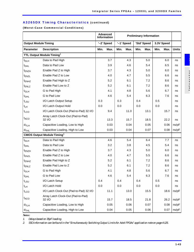
(Worst-Case Commercial Conditions)
Notes:1. Delays based on 35pF loading.2. SSO information can be found in the “Simultaneously Switching Output Limits for Actel FPGAs” application note on page 4-125.
Advanced Information Preliminary Information
Output Module Timing ‘–2’ Speed ‘–1’ Speed ‘Std’ Speed 3.3V Speed
Parameter Description Min. Max. Min. Max. Min. Max. Min. Max. Units
TTL Output Module Timing1
tDLH Data to Pad High 3.7 4.3 5.0 6.0 ns
tDHL Data to Pad Low 3.9 4.6 5.4 6.5 ns
tENZH Enable Pad Z to High 3.7 4.3 5.0 6.0 ns
tENZL Enable Pad Z to Low 4.0 4.7 5.5 6.6 ns
tENHZ Enable Pad High to Z 5.2 6.1 7.2 8.6 ns
tENLZ Enable Pad Low to Z 5.2 6.1 7.2 8.6 ns
tGLH G to Pad High 4.1 4.8 5.6 6.7 ns
tGHL G to Pad Low 4.6 5.4 6.3 7.6 ns
tLSU I/O Latch Output Setup 0.3 0.3 0.4 0.5 ns
tLH I/O Latch Output Hold 0.0 0.0 0.0 0.0 ns
tLCO I/O Latch Clock-Out (Pad-to-Pad) 32 I/O 9.4 11.0 13.1 15.7 ns
tACOArray Latch Clock-Out (Pad-to-Pad) 32 I/O 13.3 15.7 18.5 22.2 ns
dTLH Capacitive Loading, Low to High 0.03 0.04 0.05 0.06 ns/pF
dTHL Capacitive Loading, High to Low 0.03 0.04 0.07 0.08 ns/pF
CMOS Output Module Timing1
tDLH Data to Pad High 4.6 5.4 6.4 7.7 ns
tDHL Data to Pad Low 3.2 3.8 4.5 5.4 ns
tENZH Enable Pad Z to High 3.7 4.3 5.0 6.0 ns
tENZL Enable Pad Z to Low 4.0 4.7 5.5 6.6 ns
tENHZ Enable Pad High to Z 5.2 6.1 7.2 8.6 ns
tENLZ Enable Pad Low to Z 5.2 6.1 7.2 8.6 ns
tGLH G to Pad High 4.1 4.8 5.6 6.7 ns
tGHL G to Pad Low 4.6 5.4 6.3 7.6 ns
tLSU I/O Latch Setup 0.4 0.4 0.4 0.5 ns
tLH I/O Latch Hold 0.0 0.0 0.0 0.0 ns
tLCO I/O Latch Clock-Out (Pad-to-Pad) 32 I/O 11.1 13.0 15.5 18.6 ns/pF
tACOArray Latch Clock-Out (Pad-to-Pad) 32 I/O 15.7 18.5 21.8 26.2 ns/pF
dTLH Capacitive Loading, Low to High 0.05 0.06 0.07 0.08 ns/pF
dTHL Capacitive Loading, High to Low 0.04 0.05 0.06 0.07 ns/pF

1-44
A1280XL Timing Characteristics
(Worst-Case Commercial Conditions, VCC = 4.75 V, TJ = 70°C)
Notes:1. For dual-module macros, use tPD1 + tRD1 + tPDn, tCO + tRD1 + tPDn, or tPD1 + tRD1 + tSUD, whichever is appropriate.2. Routing delays are for typical designs across worst-case operating conditions. These parameters should be used for estimating device
performance. Post-route timing analysis or simulation is required to determine actual worst-case performance. Post-route timing is basedon actual routing delay measurements performed on the device prior to shipment.
3. Data applies to macros based on the S-module. Timing parameters for sequential macros constructed from C-modules can be obtained fromthe DirectTime Analyzer utility.
4. Setup and hold timing parameters for the Input Buffer Latch are defined with respect to the PAD and the D input. External setup/hold timingparameters must account for delay from an external PAD signal to the G inputs. Delay from an external PAD signal to the G input subtracts(adds) to the internal setup (hold) time.
5. VCC = 3.0 V for 3.3V specifications.
Logic Module Propagation Delays1 ‘–2’ Speed ‘–1’ Speed ‘Std’ Speed 3.3V Speed5
Parameter Description Min. Max. Min. Max. Min. Max. Min. Max. Units
tPD1 Single Module 2.6 3.0 3.5 4.2 ns
tCO Sequential Clk to Q 2.6 3.0 3.5 4.2 ns
tGO Latch G to Q 2.6 3.0 3.5 4.2 ns
tRS Flip-Flop (Latch) Reset to Q 2.6 3.0 3.5 4.2 ns
Predicted Routing Delays2
tRD1 FO=1 Routing Delay 1.3 1.4 1.7 2.0 ns
tRD2 FO=2 Routing Delay 1.8 2.0 2.4 2.9 ns
tRD3 FO=3 Routing Delay 2.2 2.5 2.9 3.5 ns
tRD4 FO=4 Routing Delay 2.6 3.0 3.5 4.2 ns
tRD8 FO=8 Routing Delay 5.0 5.7 6.7 8.0 ns
Sequential Timing Characteristics3,4
tSUD Flip-Flop (Latch) Data Input Setup 0.4 0.4 0.5 0.6 ns
tHD Flip-Flop (Latch) Data Input Hold 0.0 0.0 0.0 0.0 ns
tSUENA Flip-Flop (Latch) Enable Setup 0.8 0.9 1.0 1.2 ns
tHENA Flip-Flop (Latch) Enable Hold 0.0 0.0 0.0 0.0 ns
tWCLKA Flip-Flop (Latch) Clock Active Pulse Width 3.7 4.3 4.9 5.9 ns
tWASYN Flip-Flop (Latch) Asynchronous Pulse Width
3.7 4.34.9 5.9 ns
tA Flip-Flop Clock Input Period 8.0 8.7 10 12 ns
tINH Input Buffer Latch Hold 0.0 0.0 0.0 0.0 ns
tINSU Input Buffer Latch Setup 0.3 0.4 0.4 0.5 ns
tOUTH Output Buffer Latch Hold 0.0 0.0 0.0 0.0 ns
tOUTSU Output Buffer Latch Setup 0.3 0.4 0.4 0.5 ns
fMAX Flip-Flop (Latch) Clock Frequency 200.0 167.0 130.0 110.0 MHz

1-45
Integrator Series FPGAs – 1200XL and 3200DX Familes
Inte
gra
tor
1
A1280XL Timing Characteristics (continued)
(Worst-Case Commercial Conditions)
Note:1. These parameters should be used for estimating device performance. Optimization techniques may further reduce delays by 0 to 4 ns. Routing
delays are for typical designs across worst-case operating conditions. Post-route timing analysis or simulation is required to determineactual worst-case performance. Post-route timing is based on actual routing delay measurements performed on the device prior to shipment.
Input Module Propagation Delays ‘–2’ Speed ‘–1’ Speed ‘Std’ Speed 3.3V Speed
Parameter Description Min. Max. Min. Max. Min. Max. Min. Max. Units
tINYH Pad to Y High 1.1 1.2 1.4 1.7 ns
tINYL Pad to Y Low 1.3 1.4 1.7 2.0 ns
tINGH G to Y High 2.0 2.3 2.7 3.2 ns
tINGL G to Y Low 2.6 3.0 3.5 4.2 ns
Input Module Predicted Routing Delays1
tIRD1 FO=1 Routing Delay 3.2 3.7 4.3 5.2 ns
tIRD2 FO=2 Routing Delay 3.7 4.2 4.9 5.9 ns
tIRD3 FO=3 Routing Delay 4.0 4.5 5.3 6.4 ns
tIRD4 FO=4 Routing Delay 4.6 5.2 6.1 7.3 ns
tIRD8 FO=8 Routing Delay 6.6 7.5 8.8 10.6 ns
Global Clock Network
tCKH Input Low to High FO = 32FO = 384
5.15.7
5.86.5
6.87.6
8.29.1
ns
tCKL Input High to Low FO = 32FO = 384
5.05.7
5.76.5
6.77.6
8.09.1
ns
tPWH Minimum Pulse Width High
FO = 32FO = 384
3.23.5
3.53.9
4.34.6
5.25.5
ns
tPWL Minimum Pulse Width Low FO = 32FO = 384
3.23.5
3.53.9
4.34.6
5.25.5
ns
tCKSW Maximum Skew FO = 32FO = 384
0.80.8
0.90.9
1.01.0
1.21.2
ns
tSUEXT Input Latch External Setup FO = 32FO = 384
0.00.0
0.00.0
0.00.0
0.00.0
ns
tHEXT Input Latch External Hold FO = 32FO = 384
2.63.2
2.93.7
3.44.3
4.15.2
ns
tP Minimum Period FO = 32FO = 384
6.57.2
7.48.0
8.79.6
10.411.5
ns
fMAX Maximum Frequency FO = 32FO = 384
200.0180.0
167.0150.0
143.0130.0
120.0110.0
MHz

1-46
A1280XL Timing Characteristics (continued)
(Worst-Case Commercial Conditions)
Notes:1. Delays based on 35 pF loading.2. SSO information can be found in the “Simultaneously Switching Output Limits for Actel FPGAs” application note on page 4-125.
Output Module Timing ‘–2’ Speed ‘–1’ Speed ‘Std’ Speed 3.3V Speed
Parameter Description Min. Max. Min. Max. Min. Max. Min. Max. Units
TTL Output Module Timing1
tDLH Data to Pad High 3.8 4.3 5.0 6.0 ns
tDHL Data to Pad Low 4.1 4.6 5.4 6.5 ns
tENZH Enable Pad Z to High 3.8 4.3 5.0 6.0 ns
tENZL Enable Pad Z to Low 4.1 4.7 5.5 6.6 ns
tENHZ Enable Pad High to Z 5.4 6.1 7.2 8.6 ns
tENLZ Enable Pad Low to Z 5.4 6.1 7.2 8.6 ns
tGLH G to Pad High 4.2 4.8 5.6 6.7 ns
tGHL G to Pad Low 4.7 5.4 6.3 7.6 ns
tLCO I/O Latch Clock-Out (pad-to-pad),64 clock loading
9.8 11.0 13.1 15.7 ns
tACO Array Clock-Out (pad-to-pad),64 clock loading
13.9 15.7 18.5 22.2 ns
dTLH Capacitive Loading, Low to High 0.04 0.04 0.05 0.06 ns/pF
dTHL Capacitive Loading, High to Low 0.05 0.06 0.07 0.08 ns/pF
CMOS Output Module Timing1
tDLH Data to Pad High 4.8 5.4 6.4 7.7 ns
tDHL Data to Pad Low 3.4 3.8 4.5 5.4 ns
tENZH Enable Pad Z to High 3.8 4.3 5.0 6.0 ns
tENZL Enable Pad Z to Low 4.1 4.7 5.5 6.6 ns
tENHZ Enable Pad High to Z 5.4 6.1 7.2 8.6 ns
tENLZ Enable Pad Low to Z 5.4 6.1 7.2 8.6 ns
tGLH G to Pad High 4.2 4.8 5.6 6.7 ns
tGHL G to Pad Low 4.7 5.4 6.3 7.6 ns
tLCO I/O Latch Clock-Out (pad-to-pad),64 clock loading
11.6 13.0 15.5 18.6 ns
tACO Array Clock-Out (pad-to-pad),64 clock loading
16.4 18.5 21.8 26.2 ns
dTLH Capacitive Loading, Low to High 0.05 0.06 0.07 0.08 ns/pF
dTHL Capacitive Loading, High to Low 0.05 0.05 0.06 0.07 ns/pF

1-47
Integrator Series FPGAs – 1200XL and 3200DX Familes
Inte
gra
tor
1
A32140DX Timing Characteristics
(Worst-Case Commercial Conditions)
Notes:1. For dual-module macros, use tPD1 + tRD1 + tPDn, tCO + tRD1 + tPDn, or tPD1 + tRD1 + tSUD, whichever is appropriate.2. Routing delays are for typical designs across worst-case operating conditions. These parameters should be used for estimating device
performance. Post-route timing analysis or simulation is required to determine actual worst-case performance. Post-route timing is basedon actual routing delay measurements performed on the device prior to shipment.
3. Data applies to macros based on the S-module. Timing parameters for sequential macros constructed from C-modules can be obtained fromthe DirectTime Analyzer utility.
4. Setup and hold timing parameters for the Input Buffer Latch are defined with respect to the PAD and the D input. External setup/hold timingparameters must account for delay from an external PAD signal to the G inputs. Delay from an external PAD signal to the G input subtracts(adds) to the internal setup (hold) time.
Advanced Information Preliminary Information
Logic Module Propagation Delays1 ‘–2 Speed ‘–1’ Speed ‘Std’ Speed
Parameter Description Min. Max. Min. Max. Min. Max. Units
Combinatorial Functions
tPD Internal Array Module Delay 2.6 3.0 3.5 ns
tPDD Internal Decode Module Delay 2.9 3.3 3.9 ns
Predicted Routing Delays2
tRD1 FO=1 Routing Delay 1.3 1.4 1.7 ns
tRD2 FO=2 Routing Delay 2.0 2.2 2.6 ns
tRD3 FO=3 Routing Delay 2.9 3.3 3.8 ns
tRD4 FO=4 Routing Delay 3.5 3.9 4.6 ns
tRD5 FO=8 Routing Delay 6.3 7.1 8.4 ns
tRDD Decode-to-Output Routing Delay 0.3 0.4 0.5 ns
Sequential Timing Characteristics3, 4
tCO Flip-Flop Clock-to-Output 2.6 3.0 3.5 ns
tGO Latch Gate-to-Output 2.6 3.0 3.5 ns
tSU Flip-Flop (Latch) Setup Time 0.4 0.4 0.5 ns
tH Flip-Flop (Latch) Hold Time 0.0 0.0 0.0 ns
tRO Flip-Flop (Latch) Reset to Output 2.6 3.0 3.5 ns
tSUENA Flip-Flop (Latch) Enable Setup 0.8 0.9 1.0 ns
tHENA Flip-Flop (Latch) Enable Hold 0.0 0.0 0.0 ns
tWCLKA Flip-Flop (Latch) Clock Active Pulse Width 3.7 4.2 4.9 ns
tWASYN Flip-Flop (Latch) Asynchronous Pulse Width 3.7 4.2 4.9 ns

1-48
A32140DX Timing Characteristics (continued)
(Worst-Case Commercial Conditions)
Note:1. Routing delays are for typical designs across worst-case operating conditions. These parameters should be used for estimating device
performance. Post-route timing analysis or simulation is required to determine actual worst-case performance.
Advanced Information Preliminary Information
Input Module Propagation Delays ‘–2’ Speed ‘–1’ Speed ‘Std’ Speed
Parameter Description Min. Max. Min. Max. Min. Max. Units
tINPY Input Data Pad to Y 1.3 1.4 1.7 ns
tINGO Input Latch Gate-to-Output 2.6 3.0 3.5 ns
tINH Input Latch Hold 0.0 0.0 0.0 ns
tINSU Input Latch Setup 0.3 0.3 0.4 ns
tILA Latch Active Pulse Width 3.7 4.2 4.9 ns
Input Module Predicted Routing Delays1
tIRD1 FO=1 Routing Delay 3.2 3.7 4.3 ns
tIRD2 FO=2 Routing Delay 3.7 4.2 4.9 ns
tIRD3 FO=3 Routing Delay 4.0 4.5 5.3 ns
tIRD4 FO=4 Routing Delay 4.6 5.2 6.1 ns
tIRD5 FO=8 Routing Delay 6.6 7.5 8.8 ns
Global Clock Network
tCKH Input Low to High FO=32FO=486
5.15.7
5.86.5
6.87.6
nsns
tCKL Input High to Low FO=32FO=486
5.05.7
5.76.5
6.77.6
nsns
tPW Minimum Pulse Width FO=32FO=486
3.23.5
3.73.9
4.34.6
nsns
tCKSW Maximum Skew FO=32FO=486
0.80.8
0.90.9
1.01.0
nsns
tSUEXT Input Latch External Setup FO=32FO=486
0.00.0
0.00.0
0.00.0
nsns
tHEXT Input Latch External Hold FO=32FO=486
2.63.2
2.93.7
3.44.3
nsns
tP Minimum Period (1/fmax) FO=32FO=486
6.57.2
7.48.2
8.79.6
nsns
fMAX Maximum Datapath Frequency FO=32FO=486
153.0140.0
133.0123.0
115.0105.0
MHzMHz

1-49
Integrator Series FPGAs – 1200XL and 3200DX Familes
Inte
gra
tor
1
A32140DX Timing Characteristics (continued)
(Worst-Case Commercial Conditions)
Notes:1. Delays based on 35 pF loading.2. SSO information can be found in the “Simultaneously Switching Output Limits for Actel FPGAs” application note on page 4-125.
Advanced Information Preliminary Information
Output Module Timing ‘–2 Speed ‘–1’ Speed ‘Std’ Speed
Parameter Description Min. Max. Min. Max. Min. Max. Units
TTL Output Module Timing1
tDLH Data to Pad High 3.7 4.3 5.0 ns
tDHL Data to Pad Low 3.9 4.6 5.4 ns
tENZH Enable Pad Z to High 3.7 4.3 5.0 ns
tENZL Enable Pad Z to Low 4.0 4.7 5.5 ns
tENHZ Enable Pad High to Z 5.2 6.1 7.2 ns
tENLZ Enable Pad Low to Z 5.2 6.1 7.2 ns
tGLH G to Pad High 4.1 4.8 5.6 ns
tGHL G to Pad Low 4.6 5.4 6.3 ns
tLSU I/O Latch Output Setup 0.3 0.3 0.4 ns
tLH I/O Latch Output Hold 0.0 0.0 0.0 ns
tLCO I/O Latch Clock-Out (Pad-to-Pad) 32 I/O 9.4 11.0 13.1 ns
tACO Array Latch Clock-Out (Pad-to-Pad) 32 I/O 13.3 15.7 18.5 ns
dTLH Capacitive Loading, Low to High 0.03 0.04 0.05 ns/pF
dTHL Capacitive Loading, High to Low 0.03 0.04 0.07 ns/pF
CMOS Output Module Timing1
tDLH Data to Pad High 4.6 5.4 6.4 ns
tDHL Data to Pad Low 3.2 3.8 4.5 ns
tENZH Enable Pad Z to High 3.7 4.3 5.0 ns
tENZL Enable Pad Z to Low 4.0 4.7 5.5 ns
tENHZ Enable Pad High to Z 5.2 6.1 7.2 ns
tENLZ Enable Pad Low to Z 5.2 6.1 7.2 ns
tGLH G to Pad High 4.1 4.8 5.6 ns
tGHL G to Pad Low 4.6 5.4 6.3 ns
tLSU I/O Latch Setup 0.4 0.4 0.4 ns
tLH I/O Latch Hold 0.0 0.0 0.0 ns
tLCO I/O Latch Clock-Out (Pad-to-Pad) 32 I/O 11.1 13.0 15.6 ns/pF
tACO Array Latch Clock-Out (Pad-to-Pad) 32 I/O 15.7 18.5 21.8 ns/pF
dTLH Capacitive Loading, Low to High 0.05 0.06 0.07 ns/pF
dTHL Capacitive Loading, High to Low 0.04 0.05 0.06 ns/pF

1-50
A32200DX Timing Characteristics
(Worst-Case Commercial Conditions)
Advanced Information
Logic Module Propagation Delays ‘–2 Speed ‘–1’ Speed ‘Std’ Speed
Parameter Description Min. Max. Min. Max. Min. Max. Units
Combinatorial Functions
tPD Internal Array Module Delay 2.6 3.0 3.5 ns
tPDD Internal Decode Module Delay 2.9 3.3 3.9 ns
Predicted Module Routing Delays
tRD1 FO=1 Routing Delay 2.0 2.2 2.6 ns
tRD2 FO=2 Routing Delay 2.5 2.9 3.4 ns
tRD3 FO=3 Routing Delay 2.9 3.3 3.8 ns
tRD4 FO=4 Routing Delay 3.4 3.9 4.6 ns
tRD5 FO=8 Routing Delay 6.8 7.7 9.1 ns
tRDD Decode-to-Output Routing Delay 0.3 0.4 0.5 ns
Sequential Timing Characteristics
tCO Flip-Flop Clock-to-Output 2.6 3.0 3.5 ns
tGO Latch Gate-to-Output 2.6 3.0 3.5 ns
tSU Flip-Flop (Latch) Setup Time 0.4 0.4 0.5 ns
tH Flip-Flop (Latch) Hold Time 0.0 0.0 0.0 ns
tRO Flip-Flop (Latch) Reset to Output 2.6 3.0 3.5 ns
tSUENA Flip-Flop (Latch) Enable Setup 0.8 0.9 1.0 ns
tHENA Flip-Flop (Latch) Enable Hold 0.0 0.0 0.0 ns
tWCLKA Flip-Flop (Latch) Clock Active Pulse Width 3.7 4.2 4.9 ns
tWASYN Flip-Flop (Latch) Asynchronous Pulse Width 3.7 4.2 4.9 ns

1-51
Integrator Series FPGAs – 1200XL and 3200DX Familes
Inte
gra
tor
1
A32200DX Timing Characteristics (continued)
(Worst-Case Commercial Conditions)
Advanced Information
Logic Module Timing ‘–2 Speed ‘–1’ Speed ‘Std’ Speed
Parameter Description Min. Max. Min. Max. Min. Max. Units
Synchronous SRAM Operations
tRC Read Cycle Time 7.5 8.5 10.0 ns
tWC Write Cycle Time 7.5 8.5 10.0 ns
tRCKHL Clock High/Low Time 3.8 4.3 5.0 ns
tRCO Data Valid After Clock High/Low 3.8 4.3 5.0 ns
tADSU Address/Data Setup Time 1.8 2.0 2.4 ns
tADH Address/Data Hold Time 0.0 0.0 0.0 ns
tRENSU Read Enable Setup 0.8 0.9 1.0 ns
tRENH Read Enable Hold 0.4 0.4 0.5 ns
tWENSU Write Enable Setup 2.9 3.2 3.8 ns
tWENH Write Enable Hold 0.0 0.0 0.0 ns
tBENS Block Enable Setup 2.9 3.3 3.9 ns
tBENH Block Enable Hold 0.0 0.0 0.0 ns
Asynchronous SRAM Operations
tRPD Asynchronous Access Time 9.0 10.2 12.0 ns
tRDADV Read Address Valid 9.8 11.0 13.0 ns
tADSU Address/Data Setup Time 1.8 2.0 2.4 ns
tADH Address/Data Hold Time 0.0 0.0 0.0 ns
tRENSUA Read Enable Setup to Address Valid 0.8 0.9 1.0 ns
tRENHA Read Enable Hold 0.4 0.4 0.5 ns
tWENSU Write Enable Setup 2.9 3.2 3.8 ns
tWENH Write Enable Hold 0.0 0.0 0.0 ns
tDOH Data Out Hold Time 1.4 1.5 1.8 ns

1-52
A32200DX Timing Characteristics (continued)
(Worst-Case Commercial Conditions)
Note:1. Routing delays are for typical designs across worst-case operating conditions. These parameters should be used for estimating device
performance. Post-route timing analysis or simulation is required to determine actual worst-case performance.
Advanced Information
Input Module Propagation Delays ‘–2’ Speed ‘–1’ Speed ‘Std’ Speed
Parameter Description Min. Max. Min. Max. Min. Max. Units
tINPY Input Data Pad to Y 1.3 1.4 1.7 ns
tINGO Input Latch Gate-to-Output1 2.6 3.0 3.5 ns
tINH Input Latch Hold1 0.0 0.0 0.0 ns
tINSU Input Latch Setup1 0.3 0.3 0.4 ns
tILA Latch Active Pulse Width1 3.7 4.2 4.9 ns
Input Module Predicted Routing Delays
tIRD1 FO=1 Routing Delay 3.2 3.7 4.3 ns
tIRD2 FO=2 Routing Delay 3.7 4.2 4.9 ns
tIRD3 FO=3 Routing Delay 4.0 4.5 5.3 ns
tIRD4 FO=4 Routing Delay 4.6 5.2 6.1 ns
tIRD8 FO=8 Routing Delay 6.6 7.5 8.8 ns
Global Clock Network
tCKH Input Low to High FO=32FO=635
5.15.7
5.86.5
6.87.6
nsns
tCKL Input High to Low FO=32FO=635
5.05.7
5.86.5
6.77.6
nsns
tPWH Minimum Pulse Width High FO=32FO=635
3.23.5
3.74.1
4.34.6
nsns
tPWL Minimum Pulse Width Low FO=32FO=635
3.23.5
3.74.1
4.34.6
nsns
tCKSW Maximum Skew FO=32FO=635
0.80.8
0.90.9
1.01.0
nsns
tSUEXT Input Latch External Setup FO=32FO=635
0.00.0
0.00.0
0.00.0
nsns
tHEXT Input Latch External Hold FO=32FO=635
2.63.2
2.93.7
3.44.3
nsns
tP Minimum Period (1/fmax) FO=32FO=635
6.57.2
7.48.2
8.79.6
nsns
fHMAX Maximum Datapath Frequency FO=32FO=635
153.0140.0
133.0123.0
115.0105.0
MHzMHz

1-53
Integrator Series FPGAs – 1200XL and 3200DX Familes
Inte
gra
tor
1
A32200DX Timing Characteristics (continued)
(Worst-Case Commercial Conditions)
Notes:1. Routing delays are for typical designs across worst-case operating conditions. These parameters should be used for estimating device
performance. Post-route timing analysis or simulation is required to determine actual worst-case performance.2. SSO information can be found in the “Simultaneously Switching Output Limits for Actel FPGAs” application note on page 4-125.
Advanced Information
Output Module Timing ‘–2’ Speed ‘–1’ Speed ‘Std’ Speed
Parameter Description Min. Max. Min. Max. Min. Max. Units
TTL Output Module Timing1
tDLH Data to Pad High 3.7 4.3 5.4 ns
tDHL Data to Pad Low 3.9 4.6 5.4 ns
tENZH Enable Pad Z to High 3.7 4.3 5.0 ns
tENZL Enable Pad Z to Low 4.0 4.7 5.5 ns
tENHZ Enable Pad High to Z 5.2 6.1 7.2 ns
tENLZ Enable Pad Low to Z 5.2 6.1 7.2 ns
tGLH G to Pad High 4.1 4.8 5.6 ns
tGHL G to Pad Low 4.6 5.4 6.3 ns
tLSU I/O Latch Output Setup 0.3 0.3 0.4 ns
tLH I/O Latch Output Hold 0.0 0.0 0.0 ns
tLCO I/O Latch Clock-Out (Pad-to-Pad) 32 I/O 9.4 11.0 13.1 ns
tACO Array Latch Clock-Out (Pad-to-Pad) 32 I/O 13.3 15.7 18.5 ns
dTLH Capacitive Loading, Low to High 0.03 0.04 0.05 ns/pF
dTHL Capacitive Loading, High to Low 0.03 0.04 0.07 ns/pF
tWDO Hard-Wired Wide Decode Output 0.05 ns
CMOS Output Module Timing1
tDLH Data to Pad High 4.6 5.4 6.4 ns
tDHL Data to Pad Low 3.2 3.8 4.5 ns
tENZH Enable Pad Z to High 3.7 4.3 5.0 ns
tENZL Enable Pad Z to Low 4.0 4.7 5.5 ns
tENHZ Enable Pad High to Z 5.2 6.1 7.2 ns
tENLZ Enable Pad Low to Z 5.2 6.1 7.2 ns
tGLH G to Pad High 4.1 4.8 5.6 ns
tGHL G to Pad Low 4.6 5.4 6.3 ns
tLSU I/O Latch Setup 0.4 0.4 0.4 ns
tLH I/O Latch Hold 0.0 0.0 0.0 ns
tLCO I/O Latch Clock-Out (Pad-to-Pad) 32 I/O 11.1 13.0 15.5 ns/pF
tACO Array Latch Clock-Out (Pad-to-Pad) 32 I/O 15.7 18.5 21.8 ns/pF
dTLH Capacitive Loading, Low to High 0.05 0.06 0.07 ns/pF
dTHL Capacitive Loading, High to Low 0.04 0.05 0.06 ns/pF
tWDO Hard-Wired Wide Decode Output 0.04 0.05 0.06 ns/pF

1-54
Package Pin Assignments
84-Pin PLCC Package (Top View)
1 84
84-Pin PLCC

1-55
Integrator Series FPGAs – 1200XL and 3200DX Familes
Inte
gra
tor
1
Notes:1. I/O (WD) : Denotes I/O pin with an associated Wide Decode Module2. Wide Decode I/O (WD) can also be general purpose user I/O3. NC : Denotes No Connection4. All unlisted pin numbers are user I/O’s5. MODE should be terminated to GND through a 10K resistor to enable Actionprobe usage; otherwise it can be terminated directly to GND.
84-Pin PLCC Package
PinNumber
A1225XL Function
A1240XLFunction
A3265DXFunction
A1280XL Function
2 CLKB,I/O CLKB,I/O CLKB,I/O CLKB,I/O
4 PRB,I/O PRB,I/O PRB,I/O PRB,I/O
5 I/O I/O I/O (WD) I/O
6 GND GND GND GND
8 I/O I/O I/O (WD) I/O
9 I/O I/O I/O (WD) I/O
10 DCLK,I/O DCLK,I/O DCLK,I/O DCLK,I/O
12 MODE MODE MODE MODE
22 VCC VCC VCC VCC
23 VCC VCC VCC VCC
28 GND GND GND GND
38 I/O I/O I/O (WD) I/O
39 I/O I/O I/O (WD) I/O
43 VCC VCC VCC VCC
44 I/O I/O I/O (WD) I/O
46 I/O I/O I/O (WD) I/O
47 I/O I/O I/O (WD) I/O
49 GND GND GND GND
63 GND GND GND GND
64 VCC VCC VCC VCC
65 VCC VCC VCC VCC
70 GND GND GND GND
76 SDI,I/O SDI,I/O SDI,I/O SDI,I/O
78 I/O I/O I/O (WD) I/O
79 I/O I/O I/O (WD) I/O
80 I/O I/O I/O (WD) I/O
81 PRA,I/O PRA,I/O PRA,I/O PRA,I/O
83 CLKA,I/O CLKA,I/O CLKA,I/O CLKA,I/O
84 VCC VCC VCC VCC

1-56
Package Pin Assignments (continued)
100-pin PQFP Package, 100-pin VQFP Package (Top View)
100-Pin PQFP
1100
1
100-Pin VQFP
100

1-57
Integrator Series FPGAs – 1200XL and 3200DX Familes
Inte
gra
tor
1
Notes:1. NC : Denotes No Connection2. All unlisted pin numbers are user I/O’s3. MODE should be terminated to GND through a 10K resistor to enable Actionprobe usage; otherwise it can be terminated directly to GND.
100-pin PQFP Package, 100-pin VQFP Package
Pin Number
A1225XL-PQ100Function
A1225XL-VQ100Function
A1240XL-PQ100Function
Pin Number
A1225XL-PQ100Function
A1225XL-VQ100Function
A1240XL-PQ100Function
2 DCLK, I/O MODE DCLK, I/O 64 GND VCC GND
4 MODE I/O MODE 65 VCC VCC VCC
7 I/O GND I/O 66 VCC I/O VCC
9 GND I/O GND 67 VCC I/O VCC
14 I/O VCC I/O 70 I/O GND I/O
15 I/O VCC I/O 72 GND I/O GND
16 VCC I/O VCC 77 I/O SDI, I/O I/O
17 VCC I/O VCC 79 SDI, I/O I/O SDI, I/O
20 I/O GND I/O 82 I/O GND I/O
22 GND I/O GND 84 GND I/O GND
32 I/O GND I/O 85 I/O PRA, I/O I/O
34 GND I/O GND 87 PRA, I/O CLKA, I/O PRA, I/O
38 I/O VCC I/O 88 I/O VCC I/O
40 VCC I/O VCC 89 CLKA, I/O I/O CLKA, I/O
44 I/O GND I/O 90 VCC CLKB, I/O VCC
46 GND I/O GND 92 CLKB, I/O PRB, I/O CLKB, I/O
55 I/O GND I/O 94 PRB, I/O GND PRB, I/O
57 GND I/O GND 96 GND I/O GND
62 I/O GND I/O 100 I/O DCLK, I/O I/O
63 I/O VCC I/O

1-58
Package Pin Assignments (continued)
144-Pin PQFP Package (Top View)
144
1
144-Pin PQFP

1-59
Integrator Series FPGAs – 1200XL and 3200DX Familes
Inte
gra
tor
1
Notes:1. NC : Denotes No Connection2. All unlisted pin numbers are user I/O’s3. MODE should be terminated to GND through a 10K resistor to enable Actionprobe usage; otherwise it can be terminated directly to GND.
144-Pin PQFP Package
Pin Number A1240XL Function Pin Number A1240XL Function
2 MODE 89 VCC
9 GND 90 VCC
10 GND 91 VCC
11 GND 92 VCC
18 VCC 93 VCC
19 VCC 100 GND
20 VCC 101 GND
21 VCC 102 GND
28 GND 110 SDI, I/O
29 GND 116 GND
30 GND 117 GND
44 GND 118 GND
45 GND 123 PRA, I/O
46 GND 125 CLKA, I/O
54 VCC 126 VCC
55 VCC 127 VCC
56 VCC 128 VCC
64 GND 130 CLKB, I/O
65 GND 132 PRB, I/O
79 GND 136 GND
80 GND 137 GND
81 GND 138 GND
88 GND 144 DCLK, I/O

1-60
Package Pin Assignments (continued)
160-pin PQFP Package (Top View)
Notes:1. I/O (WD) : Denotes I/O pin with an associated Wide Decode Module2. Wide Decode I/O (WD) can also be general purpose user I/O3. NC : Denotes No Connection4. All unlisted pin numbers are user I/O’s5. MODE should be terminated to GND through a 10K resistor to enable Actionprobe usage; otherwise it can be terminated directly to GND.
160
1
160-Pin PQFP

1-61
Integrator Series FPGAs – 1200XL and 3200DX Familes
Inte
gra
tor
1
160-Pin PQFP Package
Pin Number
A3265DX Function
A1280XL Function
A32140DX Function
Pin Number
A3265DX Function
A1280XL Function
A32140DX Function
2 DCLK,I/O DCLK,I/O DCLK,I/O 80 GND GND GND
4 I/O I/O I/O (WD) 82 I/O I/O TDO, I/O
5 I/O (WD) I/O I/O (WD) 83 I/O I/O I/O (WD)
6 VCC VCC VCC 84 I/O I/O I/O (WD)
7 I/O (WD) I/O I/O 86 VCC VCC VCC
11 GND GND GND 87 I/O (WD) I/O I/O
13 I/O (WD) I/O I/O (WD) 88 I/O (WD) I/O I/O (WD)
14 I/O (WD) I/O I/O (WD) 89 GND GND GND
16 PRB,I/O PRB,I/O PRB,I/O 92 I/O (WD) I/O I/O
18 CLKB,I/O CLKB,I/O CLKB,I/O 93 I/O (WD) I/O I/O
20 VCC VCC VCC 96 I/O (WD) I/O I/O (WD)
21 CLKA,I/O CLKA,I/O CLKA,I/O 97 I/O (WD) I/O I/O
23 PRA,I/O PRA,I/O PRA,I/O 98 VCC VCC VCC
24 I/O I/O I/O (WD) 99 GND GND GND
25 I/O (WD) I/O I/O (WD) 106 I/O (WD) I/O I/O (WD)
26 I/O (WD) I/O I/O 107 I/O (WD) I/O I/O (WD)
29 I/O (WD) I/O I/O (WD) 109 GND GND GND
30 GND GND GND 111 I/O (WD) I/O I/O (WD)
31 I/O (WD) I/O I/O (WD) 112 I/O (WD) I/O I/O (WD)
34 I/O (WD) I/O I/O 114 VCC VCC VCC
35 VCC VCC VCC 115 I/O I/O I/O (WD)
36 I/O (WD) I/O I/O (WD) 116 I/O I/O I/O (WD)
37 I/O I/O I/O (WD) 118 I/O I/O TDI, I/O
38 SDI,I/O SDI,I/O SDI,I/O 119 I/O I/O TMS, I/O
40 GND GND GND 120 GND GND GND
44 GND GND GND 125 GND GND GND
49 GND GND GND 130 GND GND GND
54 VCC VCC VCC 135 VCC VCC VCC
57 VCC VCC VCC 138 VCC VCC VCC
58 VCC VCC VCC 139 VCC VCC VCC
59 GND GND GND 140 GND GND GND
60 VCC VCC VCC 145 GND GND GND
61 GND GND GND 150 VCC VCC VCC
62 I/O I/O TCK, I/O 155 GND GND GND
64 GND GND GND 159 MODE MODE MODE
69 GND GND GND 160 GND GND GND

1-62
Package Pin Assignments (continued)
208-Pin PQFP Package, 208-pin RQFP Package (Top View)
Notes:1. I/O (WD) : Denotes I/O pin with an associated Wide Decode Module2. Wide Decode I/O (WD) can also be general purpose user I/O3. NC : Denotes No Connection4. All unlisted pin numbers are user I/O’s5. MODE should be terminated to GND through a 10K resistor to enable Actionprobe usage; otherwise it can be terminated directly to GND.6. RQFP has an exposed circular metal heatsink on the top surface.
208-Pin PQFP 208-Pin RQFP
1208

1-63
Integrator Series FPGAs – 1200XL and 3200DX Familes
Inte
gra
tor
1
208-Pin PQFP Package, 208-pin RQFP Package
Pin NumberA1280XL Function
A32140DX Function
A32200DX-PQ208 Function
A32200DX-RQ208 Function Pin Number
A1280XL Function
A32140DX Function
A32200DX-PQ208 Function
A32200DX-RQ208 Function
1 GND GND GND I/O 104 I/O I/O I/O GND2 NC VCC VCC DCLK, I/O 105 GND GND GND I/O3 MODE MODE MODE I/O 106 NC VCC VCC TDO, I/O5 I/O I/O I/O I/O (WD) 107 I/O I/O I/O I/O (WD)6 I/O I/O I/O I/O (WD) 108 I/O I/O I/O I/O (WD)7 I/O I/O I/O VCC 110 I/O I/O I/O VCC9 NC I/O I/O I/O 112 NC I/O I/O I/O10 NC I/O I/O I/O 113 NC I/O I/O I/O11 NC I/O I/O I/O 114 NC I/O I/O I/O (WD)13 I/O I/O I/O QCLKC, I/O 115 NC I/O I/O I/O (WD)15 I/O I/O I/O I/O (WD) 117 I/O I/O I/O QCLKB, I/O16 NC I/O I/O I/O (WD) 121 I/O I/O I/O I/O (WD)17 VCC VCC VCC I/O 122 I/O I/O I/O I/O (WD)19 I/O I/O I/O I/O (WD) 126 GND GND GND I/O20 I/O I/O I/O I/O (WD) 128 I/O TCK, I/O TCK, I/O I/O22 GND GND GND PRB, I/O 129 GND GND GND VCC24 I/O I/O I/O CLKB, I/O 130 VCC VCC VCC GND26 I/O I/O I/O GND 131 GND GND GND I/O27 GND GND GND VCC 132 VCC VCC VCC I/O28 VCC VCC VCC I/O 133 VCC VCC VCC I/O29 VCC VCC VCC CLKA, I/O 136 VCC VCC VCC I/O30 I/O I/O I/O PRA, I/O 137 I/O I/O I/O I/O (WD)32 VCC VCC VCC I/O (WD) 138 I/O I/O I/O I/O (WD)33 I/O I/O I/O I/O (WD) 141 NC I/O I/O I/O (WD)38 I/O I/O I/O QCLKD, I/O 142 I/O I/O I/O I/O (WD)40 I/O I/O I/O I/O (WD) 144 I/O I/O I/O QCLKA, I/O41 NC I/O I/O I/O (WD) 146 NC I/O I/O I/O42 NC I/O I/O I/O 147 NC I/O I/O I/O43 NC I/O I/O I/O 148 NC I/O I/O I/O45 I/O I/O I/O VCC 149 NC I/O I/O VCC47 I/O I/O I/O I/O (WD) 150 GND GND GND I/O48 I/O I/O I/O I/O (WD) 151 I/O I/O I/O I/O (WD)50 NC I/O I/O SDI, I/O 152 I/O I/O I/O I/O (WD)51 NC I/O I/O I/O 154 I/O I/O I/O TDI, I/O52 GND GND GND GND 155 I/O I/O I/O TMS, I/O53 GND GND GND I/O 156 I/O I/O I/O GND54 I/O TMS, I/O TMS, I/O I/O 157 GND GND GND VCC55 I/O TDI, I/O TDI, I/O I/O 159 SDI,I/O SDI,I/O SDI,I/O I/O57 I/O I/O (WD) I/O (WD) I/O 161 I/O I/O (WD) I/O (WD) I/O58 I/O I/O (WD) I/O (WD) I/O 162 I/O I/O (WD) I/O (WD) I/O59 I/O I/O I/O GND 164 VCC VCC VCC I/O60 VCC VCC VCC I/O 165 NC I/O I/O I/O61 NC I/O I/O I/O 166 NC I/O I/O I/O62 NC I/O I/O I/O 168 I/O I/O (WD) I/O (WD) I/O65 I/O I/O QCLKA, I/O I/O 169 I/O I/O (WD) I/O (WD) I/O66 I/O I/O (WD) I/O (WD) I/O 171 NC I/O QCLKD, I/O I/O67 NC I/O (WD) I/O (WD) I/O 176 I/O I/O (WD) I/O (WD) I/O68 NC I/O I/O I/O 177 I/O I/O (WD) I/O (WD) I/O70 I/O I/O (WD) I/O (WD) I/O 178 PRA,I/O PRA,I/O PRA,I/O VCC71 I/O I/O (WD) I/O (WD) I/O 180 CLKA,I/O CLKA,I/O CLKA,I/O I/O74 I/O I/O I/O VCC 181 NC I/O I/O VCC77 I/O I/O I/O VCC 182 NC VCC VCC VCC78 GND GND GND VCC 183 VCC VCC VCC I/O79 VCC VCC VCC VCC 184 GND GND GND I/O80 NC VCC VCC GND 186 CLKB,I/O CLKB,I/O CLKB,I/O I/O81 I/O I/O I/O TCK, I/O 187 I/O I/O I/O GND83 I/O I/O I/O GND 188 PRB,I/O PRB,I/O PRB,I/O I/O85 I/O I/O (WD) I/O (WD) I/O 190 I/O I/O (WD) I/O (WD) I/O86 I/O I/O (WD) I/O (WD) I/O 191 I/O I/O (WD) I/O (WD) I/O89 NC I/O I/O I/O 193 NC I/O I/O I/O90 NC I/O I/O I/O 194 NC I/O (WD) I/O (WD) I/O91 I/O I/O QCLKB, I/O I/O 195 NC I/O (WD) I/O (WD) I/O93 I/O I/O (WD) I/O (WD) I/O 196 I/O I/O QCLKC, I/O I/O94 I/O I/O (WD) I/O (WD) I/O 197 NC I/O I/O I/O95 NC I/O I/O I/O 201 NC I/O I/O I/O96 NC I/O I/O I/O 202 VCC VCC VCC I/O97 NC I/O I/O I/O 203 I/O I/O (WD) I/O (WD) I/O98 VCC VCC VCC I/O 204 I/O I/O (WD) I/O (WD) I/O100 I/O I/O (WD) I/O (WD) I/O 206 I/O I/O I/O MODE101 I/O I/O (WD) I/O (WD) I/O 207 DCLK,I/O DCLK,I/O DCLK,I/O VCC103 I/O TDO, I/O TDO, I/O VCC 208 I/O I/O I/O GND

1-64
Package Pin Assignments (continued)
240-Pin RQFP Package (Top View)
Notes:1. I/O (WD) : Denotes I/O pin with an associated Wide Decode Module2. Wide Decode I/O (WD) can also be general purpose user I/O3. NC : Denotes No Connection4. All unlisted pin numbers are user I/O’s5. MODE should be terminated to GND through a 10K resistor to enable Actionprobe usage; otherwise it can be terminated directly to GND.6. RQFP has an exposed circular metal heatsink on the top surface.
240-Pin RQFP
Exposed Heatsink
1240
• • •
• • •• • •
• • •

1-65
Integrator Series FPGAs – 1200XL and 3200DX Familes
Inte
gra
tor
1
240-Pin RQFP Package
Pin Number A32200DX Function Pin Number A32200DX Function
2 DCLK, I/O 119 GND
6 I/O (WD) 120 GND
7 I/O (WD) 121 GND
8 VCC 123 TDO, I/O
15 QCLKC, I/O 125 I/O (WD)
17 I/O (WD) 126 I/O (WD)
18 I/O (WD) 128 VCC
21 I/O (WD) 132 I/O (WD)
22 I/O (WD) 133 I/O (WD)
24 PRB, I/O 135 QCLKB, I/O
26 CLKB, I/O 142 I/O (WD)
28 GND 143 I/O (WD)
29 VCC 150 VCC
30 VCC 151 VCC
32 CLKA, I/O 152 GND
34 PRA, I/O 159 I/O (WD)
37 I/O (WD) 160 I/O (WD)
38 I/O (WD) 163 I/O (WD)
45 QCLKD, I/O 164 I/O (WD)
47 I/O (WD) 166 QCLKA, I/O
48 I/O (WD) 172 VCC
52 VCC 174 I/O (WD)
54 I/O (WD) 175 I/O (WD)
55 I/O (WD) 178 TDI, I/O
57 SDI, I/O 179 TMS, I/O
59 VCC 180 GND
60 GND 181 VCC
61 GND 182 GND
71 VCC 192 VCC
85 VCC 206 VCC
88 VCC 209 VCC
89 VCC 210 VCC
90 VCC 219 VCC
91 GND 227 VCC
92 TCK, I/O 237 GND
94 GND 238 MODE
108 VCC 239 VCC
118 VCC 240 GND

1-66
Package Pin Assignments (continued)
176-Pin TQFP Package (Top View)
Notes:1. I/O (WD) : Denotes I/O pin with an associated Wide Decode Module2. Wide Decode I/O (WD) can also be general purpose user I/O3. NC : Denotes No Connection4. All unlisted pin numbers are user I/O’s5. MODE should be terminated to GND through a 10K resistor to enable Actionprobe usage; otherwise it can be terminated directly to GND.
176-Pin TQFP
176
1

1-67
Integrator Series FPGAs – 1200XL and 3200DX Familes
Inte
gra
tor
1
176-pin TQFP Package
Pin Number
A1240XL Function
A3265DX Function
A1280XL Function
A32140DX Function
Pin Number
A1240XL Function
A3265DX Function
A1280XL Function
A32140DX Function
1 GND GND GND GND 97 NC I/O I/O I/O2 MODE MODE MODE MODE 101 NC NC NC I/O8 NC NC NC I/O 103 NC I/O I/O I/O10 NC NC I/O I/O 106 GND GND GND GND11 NC NC I/O I/O 107 NC I/O I/O I/O13 NC VCC VCC VCC 108 NC I/O I/O TCK, I/O18 GND GND GND GND 109 GND GND GND GND19 NC I/O I/O I/O 110 VCC VCC VCC VCC20 NC I/O I/O I/O 111 GND GND GND GND22 NC I/O I/O I/O 112 VCC VCC VCC VCC23 GND GND GND GND 113 VCC VCC VCC VCC24 NC VCC VCC VCC 114 NC I/O I/O I/O25 VCC VCC VCC VCC 115 NC I/O I/O I/O26 NC I/O I/O I/O 116 NC VCC VCC VCC27 NC I/O I/O I/O 117 I/O NC I/O I/O28 VCC VCC VCC VCC 121 NC NC NC I/O29 NC NC I/O I/O 124 NC NC I/O I/O33 NC NC NC I/O 125 NC NC I/O I/O37 NC NC I/O I/O 126 NC NC NC I/O38 NC NC NC I/O 133 GND GND GND GND45 GND GND GND GND 135 SDI,I/O SDI,I/O SDI,I/O SDI,I/O46 I/O I/O I/O TMS, I/O 136 NC NC I/O I/O47 I/O I/O I/O TDI, I/O 137 I/O I/O I/O I/O (WD)48 I/O NC I/O I/O 138 I/O I/O I/O I/O (WD)49 I/O I/O I/O I/O (WD) 139 I/O I/O (WD) I/O I/O50 I/O I/O I/O I/O (WD) 140 NC VCC VCC VCC52 NC VCC VCC VCC 141 I/O I/O (WD) I/O I/O54 NC I/O (WD) I/O I/O 143 NC I/O I/O I/O55 NC I/O (WD) I/O I/O (WD) 144 NC I/O (WD) I/O I/O (WD)56 I/O I/O I/O I/O (WD) 145 NC NC NC I/O (WD)57 NC NC NC I/O 146 I/O I/O (WD) I/O I/O59 I/O I/O (WD) I/O I/O (WD) 147 NC I/O I/O I/O60 I/O I/O (WD) I/O I/O (WD) 149 I/O I/O (WD) I/O I/O61 NC I/O I/O I/O 150 I/O I/O (WD) I/O I/O (WD)64 NC I/O I/O I/O 151 NC I/O I/O I/O (WD)66 NC I/O I/O I/O 152 PRA,I/O PRA,I/O PRA,I/O PRA,I/O67 GND GND GND GND 154 CLKA,I/O CLKA,I/O CLKA,I/O CLKA,I/O68 VCC VCC VCC VCC 155 VCC VCC VCC VCC69 I/O I/O (WD) I/O I/O (WD) 156 GND GND GND GND70 I/O I/O (WD) I/O I/O (WD) 158 CLKB,I/O CLKB,I/O CLKB,I/O CLKB,I/O73 I/O I/O (WD) I/O I/O 160 PRB,I/O PRB,I/O PRB,I/O PRB,I/O74 NC NC I/O I/O 161 NC I/O I/O I/O (WD)75 I/O I/O (WD) I/O I/O 162 I/O I/O (WD) I/O I/O (WD)77 NC NC NC I/O (WD) 163 I/O I/O (WD) I/O I/O78 NC NC I/O I/O (WD) 165 NC NC NC I/O (WD)80 NC I/O (WD) I/O I/O 166 NC I/O I/O I/O (WD)81 I/O I/O (WD) I/O I/O 168 NC I/O I/O I/O82 NC VCC VCC VCC 169 I/O I/O (WD) I/O I/O84 I/O I/O I/O I/O (WD) 170 NC VCC VCC VCC85 I/O I/O I/O I/O (WD) 171 I/O I/O (WD) I/O I/O (WD)86 NC NC I/O I/O 172 I/O I/O I/O I/O (WD)87 I/O I/O I/O TDO, I/O 173 NC NC I/O I/O89 GND GND GND GND 175 DCLK,I/O DCLK,I/O DCLK,I/O DCLK,I/O96 NC NC I/O I/O

1-68
Package Pin Assignments (continued)
100-Pin CPGA (Top View)
Signal Pad Number Location
PRA or I/O 85 A7
PRB or I/O 92 A4
MODE 2 C2
SDI or I/O 77 C8
DCLK or I/O 100 C3
CLKA or I/O 87 C6
CLKB or I/O 90 D6
GND 7, 20, 32, 44, 55, 70, 82, 94 E3, G3, J5, J7, G9, F11, D10, C7, C5
VCC 15, 38, 64, 88 F3, G1, K6, F9, F10, E11, B6
Notes:
1. Unused I/O pins are designated as outputs by ALS and are driven low.
2. All unassigned pins are available for use as I/Os.
3. MODE = GND, except during device programming or debugging.
1
A
2 3 4 5 6 7 8 9 10 11
B
C
D
E
F
G
H
J
K
L
A
B
C
D
E
F
G
H
J
K
L
100-Pin CPGA
1 2 3 4 5 6 7 8 9 10 11
Orientation Pin

1-69
Integrator Series FPGAs – 1200XL and 3200DX Familes
Inte
gra
tor
1
Package Pin Assignments (continued)
132-Pin CPGA (Top View)
Signal Pad Number Location
PRA or I/O 113 B8
PRB or I/O 121 C6
MODE 2 A1
SDI or I/O 101 B12
DCLK or I/O 132 C3
CLKA or I/O 115 B7
CLKB or I/O 119 B6
GND 9, 10, 26, 27, 41, 58, 59, 73, 74, 92, 93, 107, 108, 125, 126
E3, F4, J2, J3, L5, L9, M9, K12, J11, H13, E12, E11, C9, B9, B5, C5
VCC 18, 19, 49, 50, 83, 84, 116, 117 G3, G2, G4, L7, K7, G10, G11, G12, G13, D7, C7
Notes:
1. Unused I/O pins are designated as outputs by ALS and are driven low.
2. All unassigned pins are available for use as I/Os.
3. MODE = GND, except during device programming or debugging.
132-Pin CPGA
A
B
C
D
E
F
G
H
J
K
L
M
N
A
B
C
D
E
F
G
H
J
K
L
M
N
Orientation Pin
1 2 3 4 5 6 7 8 9 10 11 12 13
1 2 3 4 5 6 7 8 9 10 11 12 13

1-70
Package Pin Assignments (continued)
176-Pin CPGA (Top View)
Signal Pad Number Location
PRA or I/O 152 C9
PRB or I/O 160 D7
MODE 2 C3
SDI or I/O 135 B14
DCLK or I/O 175 B3
CLKA or I/O 154 A9
CLKB or I/O 158 B8
GND 1, 8, 18, 23, 33, 38, 45, 57, 67, 77, 89101, 106, 111, 121, 126, 133, 145, 156, 165
D4, E4, G4, H4, K4, L4, M4, M6, M8, M10, M12K12, J12, J13, H12, F12, E12, D12, D10, C8, D6
VCC 13, 24, 28, 52, 68, 82, 112, 116, 140, 155, 170F4, H2, H3, J4, M5, N8, M11, J14, H13, H14, G12, D11, D8, D5
Notes:
1. Unused I/O pins are designated as outputs by ALS and are driven low.
2. All unassigned pins are available for use as I/Os.
3. MODE = GND, except during device programming or debugging.
1
A
2 3 4 5 6 7 8 9 10 11
B
C
D
E
F
G
H
J
K
L
176-Pin CPGA
1 2 3 4 5 6 7 8 9 10 11
12
12
13
13
14
14
15
15
M
N
P
R
A
B
C
D
E
F
G
H
J
K
L
M
N
P
R

1-71
Integrator Series FPGAs – 1200XL and 3200DX Familes
Inte
gra
tor
1
Package Pin Assignments (continued)
172-Pin CQFP
Signal Pad Number
CLKA or I/O 150
CLKB or I/O 154
DCLK or I/O 171
GND 7, 17, 22, 32, 37, 55, 65, 75, 98, 103, 106, 118, 123, 141, 152, 161
MODE 1
PRA or I/O 148
PRB or I/O 156
SDI or I/O 131
VCC 12, 23, 24, 27, 50, 66, 80, 107, 109, 110, 113, 136, 151, 166
Notes:
1. Unused I/O pins are designated as outputs by ALS and are driven low.
2. All unassigned pins are available for use as I/Os.
3. MODE = GND, except during device programming or debugging.
172-Pin CQFP
Pin #1 Index
172
1

1-72