Embed Size (px)
Citation preview
Revision 2.45
September 2012
Intel® 82580EB/82580DB Gigabit Ethernet Controller Specification Update
LAN Access Division (LAD)
Legal - Intel® 83580EB/82580DB GbE Controller
Intel® 83580EB/82580DB GbE Controller Revision 2.45Specification Update September 20122
Legal
INFORMATION IN THIS DOCUMENT IS PROVIDED IN CONNECTION WITH INTEL PRODUCTS. NO LICENSE, EXPRESS OR IMPLIED, BY ESTOPPEL OR OTHERWISE, TO ANY INTELLECTUAL PROPERTY RIGHTS IS GRANTED BY THIS DOCUMENT. EXCEPT AS PROVIDED IN INTEL'S TERMS AND CONDITIONS OF SALE FOR SUCH PRODUCTS, INTEL ASSUMES NO LIABILITY WHATSOEVER AND INTEL DISCLAIMS ANY EXPRESS OR IMPLIED WARRANTY, RELATING TO SALE AND/OR USE OF INTEL PRODUCTS INCLUDING LIABILITY OR WARRANTIES RELATING TO FITNESS FOR A PARTICULAR PURPOSE, MERCHANTABILITY, OR INFRINGEMENT OF ANY PATENT, COPYRIGHT OR OTHER INTELLECTUAL PROPERTY RIGHT.
A "Mission Critical Application" is any application in which failure of the Intel Product could result, directly or indirectly, in personal injury or death. SHOULD YOU PURCHASE OR USE INTEL'S PRODUCTS FOR ANY SUCH MISSION CRITICAL APPLICATION, YOU SHALL INDEMNIFY AND HOLD INTEL AND ITS SUBSIDIARIES, SUBCONTRACTORS AND AFFILIATES, AND THE DIRECTORS, OFFICERS, AND EMPLOYEES OF EACH, HARMLESS AGAINST ALL CLAIMS COSTS, DAMAGES, AND EXPENSES AND REASONABLE ATTORNEYS' FEES ARISING OUT OF, DIRECTLY OR INDIRECTLY, ANY CLAIM OF PRODUCT LIABILITY, PERSONAL INJURY, OR DEATH ARISING IN ANY WAY OUT OF SUCH MISSION CRITICAL APPLICATION, WHETHER OR NOT INTEL OR ITS SUBCONTRACTOR WAS NEGLIGENT IN THE DESIGN, MANUFACTURE, OR WARNING OF THE INTEL PRODUCT OR ANY OF ITS PARTS.
Intel may make changes to specifications and product descriptions at any time, without notice. Designers must not rely on the absence or characteristics of any features or instructions marked "reserved" or "undefined". Intel reserves these for future definition and shall have no responsibility whatsoever for conflicts or incompatibilities arising from future changes to them. The information here is subject to change without notice. Do not finalize a design with this information.
The products described in this document may contain design defects or errors known as errata which may cause the product to deviate from published specifications. Current characterized errata are available on request.
Contact your local Intel sales office or your distributor to obtain the latest specifications and before placing your product order.
Copies of documents which have an order number and are referenced in this document, or other Intel literature, may be obtained by calling 1-800-548-4725, or go to: http://www.intel.com/design/literature.htm.
Intel and Intel logo are trademarks or registered trademarks of Intel Corporation or its subsidiaries in the United States and other countries.
* Other names and brands may be claimed as the property of others.
Copyright © 2009-2012; Intel Corporation. All Rights Reserved.
Intel® 83580EB/82580DB GbE Controller - Revisions
Revision 2.45 Intel® 83580EB/82580DB GbE ControllerSeptember 2012 Specification Update
3
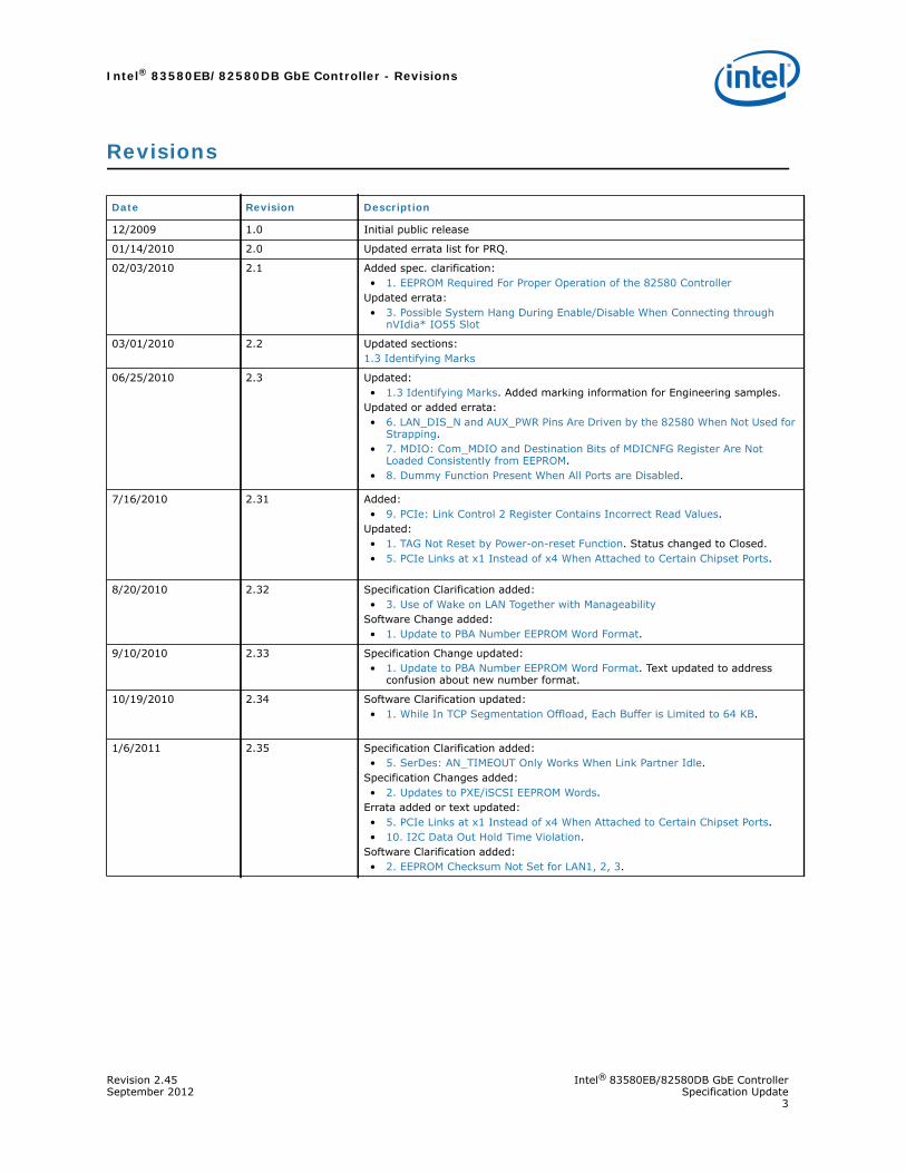
Revisions
Date Revision Description
12/2009 1.0 Initial public release
01/14/2010 2.0 Updated errata list for PRQ.
02/03/2010 2.1 Added spec. clarification:• 1. EEPROM Required For Proper Operation of the 82580 Controller
Updated errata:• 3. Possible System Hang During Enable/Disable When Connecting through
nVIdia* IO55 Slot
03/01/2010 2.2 Updated sections:1.3 Identifying Marks
06/25/2010 2.3 Updated:• 1.3 Identifying Marks. Added marking information for Engineering samples.
Updated or added errata:• 6. LAN_DIS_N and AUX_PWR Pins Are Driven by the 82580 When Not Used for
Strapping. • 7. MDIO: Com_MDIO and Destination Bits of MDICNFG Register Are Not
Loaded Consistently from EEPROM. • 8. Dummy Function Present When All Ports are Disabled.
7/16/2010 2.31 Added: • 9. PCIe: Link Control 2 Register Contains Incorrect Read Values.
Updated:• 1. TAG Not Reset by Power-on-reset Function. Status changed to Closed.• 5. PCIe Links at x1 Instead of x4 When Attached to Certain Chipset Ports.
8/20/2010 2.32 Specification Clarification added:• 3. Use of Wake on LAN Together with Manageability
Software Change added:• 1. Update to PBA Number EEPROM Word Format.
9/10/2010 2.33 Specification Change updated:• 1. Update to PBA Number EEPROM Word Format. Text updated to address
confusion about new number format.
10/19/2010 2.34 Software Clarification updated:• 1. While In TCP Segmentation Offload, Each Buffer is Limited to 64 KB.
1/6/2011 2.35 Specification Clarification added:• 5. SerDes: AN_TIMEOUT Only Works When Link Partner Idle.
Specification Changes added:• 2. Updates to PXE/iSCSI EEPROM Words.
Errata added or text updated:• 5. PCIe Links at x1 Instead of x4 When Attached to Certain Chipset Ports.• 10. I2C Data Out Hold Time Violation.
Software Clarification added:• 2. EEPROM Checksum Not Set for LAN1, 2, 3.
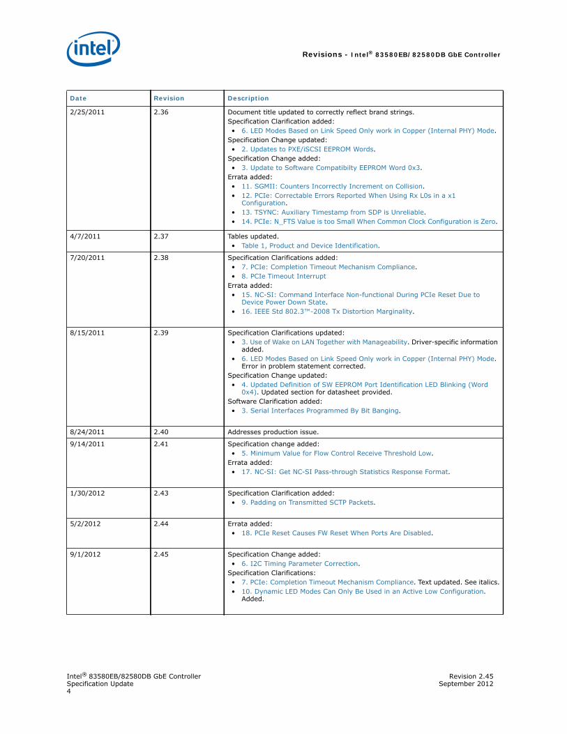
Revisions - Intel® 83580EB/82580DB GbE Controller
Intel® 83580EB/82580DB GbE Controller Revision 2.45Specification Update September 20124
2/25/2011 2.36 Document title updated to correctly reflect brand strings.Specification Clarification added:• 6. LED Modes Based on Link Speed Only work in Copper (Internal PHY) Mode.
Specification Change updated:• 2. Updates to PXE/iSCSI EEPROM Words.
Specification Change added:• 3. Update to Software Compatibilty EEPROM Word 0x3.
Errata added:• 11. SGMII: Counters Incorrectly Increment on Collision. • 12. PCIe: Correctable Errors Reported When Using Rx L0s in a x1
Configuration. • 13. TSYNC: Auxiliary Timestamp from SDP is Unreliable. • 14. PCIe: N_FTS Value is too Small When Common Clock Configuration is Zero.
4/7/2011 2.37 Tables updated.• Table 1, Product and Device Identification.
7/20/2011 2.38 Specification Clarifications added:• 7. PCIe: Completion Timeout Mechanism Compliance. • 8. PCIe Timeout Interrupt
Errata added:• 15. NC-SI: Command Interface Non-functional During PCIe Reset Due to
Device Power Down State.• 16. IEEE Std 802.3™-2008 Tx Distortion Marginality.
8/15/2011 2.39 Specification Clarifications updated:• 3. Use of Wake on LAN Together with Manageability. Driver-specific information
added.• 6. LED Modes Based on Link Speed Only work in Copper (Internal PHY) Mode.
Error in problem statement corrected.Specification Change updated:• 4. Updated Definition of SW EEPROM Port Identification LED Blinking (Word
0x4). Updated section for datasheet provided.Software Clarification added:• 3. Serial Interfaces Programmed By Bit Banging.
8/24/2011 2.40 Addresses production issue.
9/14/2011 2.41 Specification change added:• 5. Minimum Value for Flow Control Receive Threshold Low.
Errata added:• 17. NC-SI: Get NC-SI Pass-through Statistics Response Format.
1/30/2012 2.43 Specification Clarification added:• 9. Padding on Transmitted SCTP Packets.
5/2/2012 2.44 Errata added:• 18. PCIe Reset Causes FW Reset When Ports Are Disabled.
9/1/2012 2.45 Specification Change added:• 6. I2C Timing Parameter Correction.
Specification Clarifications:• 7. PCIe: Completion Timeout Mechanism Compliance. Text updated. See italics.• 10. Dynamic LED Modes Can Only Be Used in an Active Low Configuration.
Added.
Date Revision Description
Intel® 83580EB/82580DB GbE Controller - Introduction
Revision 2.45 Intel® 83580EB/82580DB GbE ControllerSeptember 2012 Specification Update
5
1.1 Introduction
This document is an update to the product datasheet. It is intended for use by system manufacturers and software developers. All product documents are subject to frequent revision. Be sure you have the latest information before finalizing your design.
References to PCIe* in this document refer to PCIe v2.0 (5Gbps).
1.2 Product and Device Identification
Table 1. Product and Device Identification
MM# Stepping Top Marking Spec # Intel SPEED iPN
Status & Media Description
905781 A1 NH82580EB S LH5P E69716-003 Production, T&R 1 Gbs, 4-port
905782 A1 NH82580EB S LH5Q E69716-004 Production, Tray
905783 A1 NH82580EK S LH5R E82069-002 Production, T&R 1 Gbs 4-port SERDES
905784 A1 NH82580EK S LH5S E82069-003 Production, Tray
905785 A1 NH82580DB S LH5T E82070-002 Production, T&R 1 Gbs, 2-port
905786 A1 NH82580DB S LH5U E82070-003 Production, Tray
904983 A1 NH82580EB Q MQR E69716-002 Engineering, Tray 1 Gbs, 4 port
907335 A1 NH82580EK Q MQT E82069-001 Engineering, Tray 1 Gbs, 4-port SERDES
907334 A1 NH82580DB Q MQS E82070-001 Engineering, Tray 1 Gbs, 2-port
903315 A0 NH82580EB Q LSY E69716-001 Engineering, Tray 1 Gbs, 4-port
Identifying Marks - Intel® 83580EB/82580DB GbE Controller
Intel® 83580EB/82580DB GbE Controller Revision 2.45Specification Update September 20126
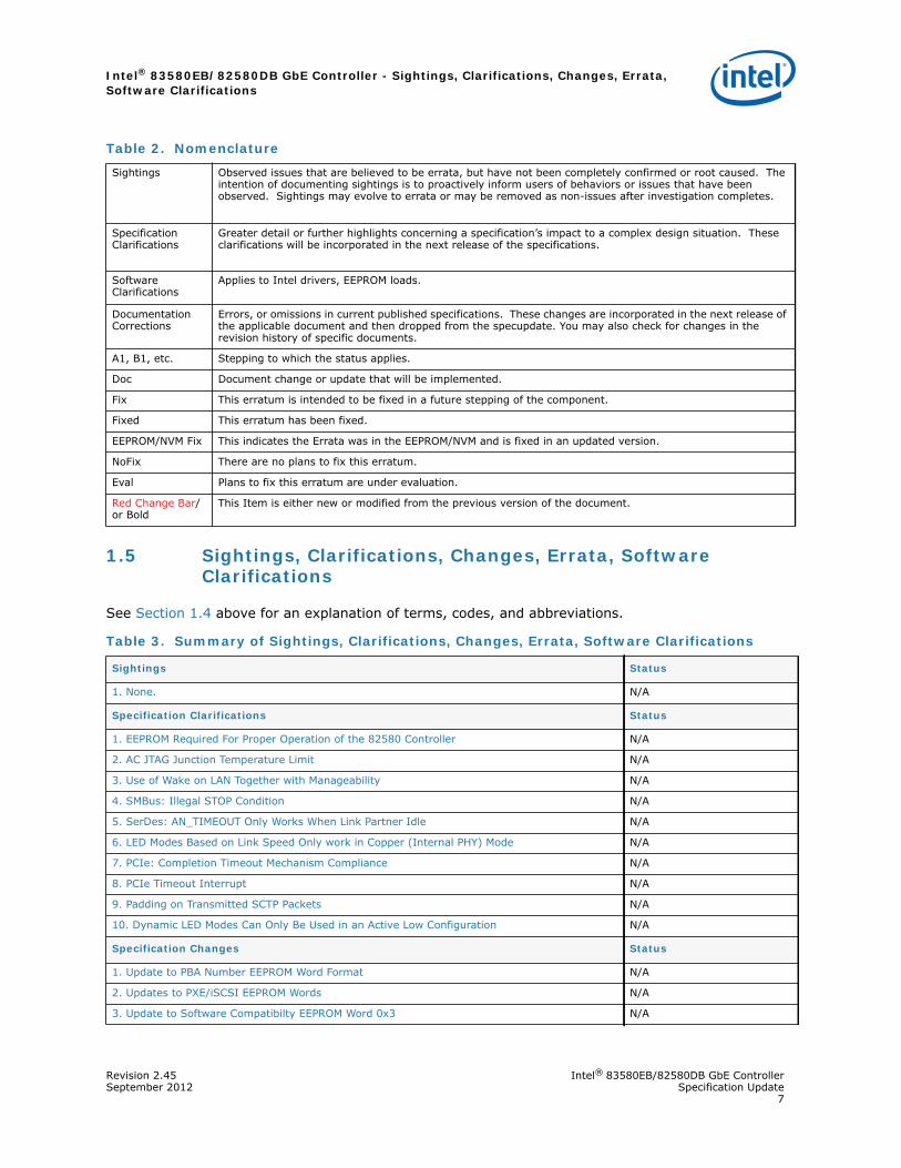
1.3 Identifying Marks
Refer to Figure 1:
1.4 Nomenclature Used In This Document
This document uses specific terms, codes, and abbreviations to describe changes, errata, sightings and/or clarifications that apply to a specific silicon stepping. See Table 2 for a description.
Engineering Samples Production
Figure 1. Sample Component Diagram Illustrating Identifying Marks
Line 1 “intel”
Line 2 Marketing Name
Line 3 Fab Lot Number “XXXXXXXXX” (Wafer Lot no. concatenated with Assembler vendor code)
Line 4 Assembly Date Code YYWW; Engineering samples have additional Intel data.
Line 5 Copyright line; includes two number date code and the Pb-free mark (e1)
Line 6 Country of Origin
Table 2. Nomenclature
Name Description
Specification Changes
Modifications to the current published specifications. These changes will be incorporated in the next release of the specifications.
Errata Design defects or errors. Errata may cause device behavior to deviate from published specifications. Hardware and software designed to be used with any given stepping must assume that all errata documented for that stepping are present on all devices.
Intel® 83580EB/82580DB GbE Controller - Sightings, Clarifications, Changes, Errata, Software Clarifications
Revision 2.45 Intel® 83580EB/82580DB GbE ControllerSeptember 2012 Specification Update
7
1.5 Sightings, Clarifications, Changes, Errata, Software Clarifications
See Section 1.4 above for an explanation of terms, codes, and abbreviations.
Sightings Observed issues that are believed to be errata, but have not been completely confirmed or root caused. The intention of documenting sightings is to proactively inform users of behaviors or issues that have been observed. Sightings may evolve to errata or may be removed as non-issues after investigation completes.
Specification Clarifications
Greater detail or further highlights concerning a specification’s impact to a complex design situation. These clarifications will be incorporated in the next release of the specifications.
Software Clarifications
Applies to Intel drivers, EEPROM loads.
Documentation Corrections
Errors, or omissions in current published specifications. These changes are incorporated in the next release of the applicable document and then dropped from the specupdate. You may also check for changes in the revision history of specific documents.
A1, B1, etc. Stepping to which the status applies.
Doc Document change or update that will be implemented.
Fix This erratum is intended to be fixed in a future stepping of the component.
Fixed This erratum has been fixed.
EEPROM/NVM Fix This indicates the Errata was in the EEPROM/NVM and is fixed in an updated version.
NoFix There are no plans to fix this erratum.
Eval Plans to fix this erratum are under evaluation.
Red Change Bar/or Bold
This Item is either new or modified from the previous version of the document.
Table 3. Summary of Sightings, Clarifications, Changes, Errata, Software Clarifications
Sightings Status
1. None. N/A
Specification Clarifications Status
1. EEPROM Required For Proper Operation of the 82580 Controller N/A
2. AC JTAG Junction Temperature Limit N/A
3. Use of Wake on LAN Together with Manageability N/A
4. SMBus: Illegal STOP Condition N/A
5. SerDes: AN_TIMEOUT Only Works When Link Partner Idle N/A
6. LED Modes Based on Link Speed Only work in Copper (Internal PHY) Mode N/A
7. PCIe: Completion Timeout Mechanism Compliance N/A
8. PCIe Timeout Interrupt N/A
9. Padding on Transmitted SCTP Packets N/A
10. Dynamic LED Modes Can Only Be Used in an Active Low Configuration N/A
Specification Changes Status
1. Update to PBA Number EEPROM Word Format N/A
2. Updates to PXE/iSCSI EEPROM Words N/A
3. Update to Software Compatibilty EEPROM Word 0x3 N/A
Table 2. Nomenclature
Sightings - Intel® 83580EB/82580DB GbE Controller
Intel® 83580EB/82580DB GbE Controller Revision 2.45Specification Update September 20128
1.5.1 Sightings
1. None.
1.5.2 Specification Clarifications
1. EEPROM Required For Proper Operation of the 82580 Controller
Clarification: Problems identified in the PCIe logic were resolved by implementing workarounds in EEPROM. Without these workarounds, the PCIe bus may not properly configure and the possibility exists that the controller will not negotiate a PCIe connection. This leaves the 82580 inaccessible.
Workaround: Use an EEPROM with the workarounds (v3.22 or greater) to ensure proper device configuration.
4. Updated Definition of SW EEPROM Port Identification LED Blinking (Word 0x4) N/A
5. Minimum Value for Flow Control Receive Threshold Low N/A
6. I2C Timing Parameter Correction N/A
Errata
1. TAG Not Reset by Power-on-reset Function Closed
2. MNG Reset Clears Resource Grant With No Feedback A1 NoFix
3. Possible System Hang During Enable/Disable When Connecting through nVIdia* IO55 Slot A1 NoFix
4. SMBus: EEPROM Not Written On ARP If the EEPROM Semaphore Is Taken by SW A1 NoFix
5. PCIe Links at x1 Instead of x4 When Attached to Certain Chipset Ports A1 NoFix
6. LAN_DIS_N and AUX_PWR Pins Are Driven by the 82580 When Not Used for Strapping A1 NoFix
7. MDIO: Com_MDIO and Destination Bits of MDICNFG Register Are Not Loaded Consistently from EEPROM
A1 NoFix
8. Dummy Function Present When All Ports are Disabled A1 NoFix
9. PCIe: Link Control 2 Register Contains Incorrect Read Values A1 NoFix
10. I2C Data Out Hold Time Violation A1 NoFix
11. SGMII: Counters Incorrectly Increment on Collision A1 NoFix
12. PCIe: Correctable Errors Reported When Using Rx L0s in a x1 Configuration A1 NoFix
13. TSYNC: Auxiliary Timestamp from SDP is Unreliable A1 NoFix
14. PCIe: N_FTS Value is too Small When Common Clock Configuration is Zero A1 NoFix
15. NC-SI: Command Interface Non-functional During PCIe Reset Due to Device Power Down State
A1 NoFix
16. IEEE Std 802.3™-2008 Tx Distortion Marginality A1 NoFix
17. NC-SI: Get NC-SI Pass-through Statistics Response Format A1 NoFix
18. PCIe Reset Causes FW Reset When Ports Are Disabled Fixed in EEPROM
Software Clarifications
1. While In TCP Segmentation Offload, Each Buffer is Limited to 64 KB N/A
2. EEPROM Checksum Not Set for LAN1, 2, 3 N/A
3. Serial Interfaces Programmed By Bit Banging N/A
Table 3. Summary of Sightings, Clarifications, Changes, Errata, Software Clarifications
Intel® 83580EB/82580DB GbE Controller - Specification Clarifications
Revision 2.45 Intel® 83580EB/82580DB GbE ControllerSeptember 2012 Specification Update
9
2. AC JTAG Junction Temperature Limit
Specification: IEEE 1149.6: A Boundary-Scan Standard for Advanced Digital Networks
Clarification: AC JTAG (IEEE 1149.6) is supported only up to a junction temperature of 70'C.
Workaround: None. This is a design parameter for the hardware.
3. Use of Wake on LAN Together with Manageability
Clarification: The Wakeup Filter Control Register (WUFC) contains the NoTCO bit, which affects the behavior of the wakeup functionality when manageability is in use. Note that if manageability is not enabled, the value of NoTCO has no effect.
When NoTCO contains the hardware default value of 0b, any received packet that matches the wakeup filters will wake the system. This could cause unintended wakeups in certain situations. For example, if Directed Exact Wakeup is used and the manageability shares the host's MAC address, IPMI packets that are intended for the BMC wakes the system, which might not be the intended behavior.
When NoTCO is set to 1b, any packet that passes the manageability filter, even if it also is copied to the host, is excluded from the wakeup logic. This solves the previous problem since IPMI packets do not wake the system. However, with NoTCO=1b, broadcast packets, including broadcast magic packets, do not wake the system since they pass the manageability filters and are therefore excluded.
The Intel Windows* drivers set NoTCO by default.
If this is not not desired behavior, the EnableWakeOnManagmentOnTCO registry entry can be used to change this setting starting with Intel LAN driver SW release 15.7. Setting this registry entry to 1b causes the driver to program NoTCO to 0b. A tool to modify the registry entry can be provided.
Contact your Intel representative for access.
4. SMBus: Illegal STOP Condition
Clarification: It is important to prevent illegal STOP conditions on the SMBus interface, even when resetting the MC.
Effects of NoTCO Settings WoL NoTCO Shared MAC
Address Unicast Packet Broadcast Packet
Magic Packet 0b - OK OK
Magic Packet 1b Y No wake No wake
Magic Packet 1b N OK No wake
Directed Exact 0b Y Wake even if MNG packet. No
way to talk to BMC without waking host.
N/A
Directed Exact 0b N OK N/A
Directed Exact 1b - OK N/A
Specification Clarifications - Intel® 83580EB/82580DB GbE Controller
Intel® 83580EB/82580DB GbE Controller Revision 2.45Specification Update September 201210
Specifically, a STOP condition should never be generated by the MC during the high clock phase of an ACK cycle while reading packet data from the 82580 as part of a Receive TCO LAN packet transaction.
If this situation occurs, the 82580 replies with a NACK to all future commands until a power cycle. As a result, the SMBus interface becomes inoperable.
Ensure that this illegal sequence does not occur, even during MC reset.
5. SerDes: AN_TIMEOUT Only Works When Link Partner Idle
Clarification: The auto-negotiation timeout mechanism (PCS_LCTL.AN_TIMEOUT_EN) only works if the SerDes partner is sending idle code groups continuously for the duration of the timeout period, which is the usual case.
However, if the partner is transmitting packets, an auto-negotiation timeout will not occur since auto-negotiation is restarted at the beginning of each packet. If the partner has an application that indefinitely transmits data despite the lack of any response, it is possible that a link will not be established.
If this is a concern, the auto-negotiation timeout mechanism may be considered unreliable and an additional software mechanism could be used to disable auto-negotiation if sync is maintained without a link being established (PCS_LSTS.SYNC_OK=1b and PCS_LSTS.LINK_OK=0b) for an extended period of time.
6. LED Modes Based on Link Speed Only work in Copper (Internal PHY) Mode
Clarification: LED modes based on LINK speed work only in copper mode, not in SerDes/SGMII modes. This includes the modes LINK_10/1000. LINK_100/1000, LINK_10, LINK_100, LINK_1000 and COLLISION.
Designs using SerDes and SGMII modes requiring a Link-up indication should use LINK_UP or LINK/ACTIVITY LED modes. Using these modes results in no issues in using the LEDs to properly indicate the link is up.
7. PCIe: Completion Timeout Mechanism Compliance
Clarification: The 82580 Completion Timeout Value[3:0] must be properly set by the system BIOS in the 82580 PCIe Configuration Space Device Control 2 register (0xC8; W). Failure to do so can cause unexpected completion timeouts.
The 82580 complies with the PCIe 2.0 specification for the completion timeout mechanism and programmable timeout values. The PCIe 2.0 specification provides programmable timeout ranges between 50us to 64s with a default time range of 50us - 50ms. The 82580 defaults to a range of 16ms - 32ms.
The completion timeout value must be programmed correctly in PCIe configuration space (in Device Control 2 register); the value must be set above the expected maximum latency for completions. This ensures that the 82580 receives completions for the requests it sends out. Failure to properly set the completion timeout value can result in the device timing out prior to a completion returning.
The 82580 can be programmed to resend a completion request after a completion timeout (the original completion is assumed lost). But if the original completion arrives after a resend request, two completions may arrive for the same request; this can cause unpredictable behavior. Intel EEPROM images set the resend feature to off. Intel recommends that you do not change this setting.
For details on completion timeout operation, refer to the Datasheet.
Intel® 83580EB/82580DB GbE Controller - Specification Changes
Revision 2.45 Intel® 83580EB/82580DB GbE ControllerSeptember 2012 Specification Update
11
8. PCIe Timeout Interrupt
Clarification: The PCIe Timeout Exception (TO) bit in the PCIe Interrupt Cause (PICAUSE) register is set when a timeout occurs on an access to the address space of this port. This includes accesses initiated by the EEPROM auto-load function and manageability firmware, in addition to accesses from the PCIe interface.
This interrupt bit does not necessarily indicate a problem with a PCIe transaction and further analysis would be required to determine the source of problem.
9. Padding on Transmitted SCTP Packets
Clarification: When using the 82580EB/DB to offload the CRC calculation for transmitted SCTP packets, software should not add Ethernet padding bytes to short packets(less than 64 bytes). Instead, the TCTL.PSP bit should be set so that the 82580EB/DB pads the packets after performing the CRC calculation.
10. Dynamic LED Modes Can Only Be Used in an Active Low Configuration
Clarification: In any of the dynamic LED modes (FILTER_ACTIVITY, LINK/ACTIVITY, COLLISION, ACTIVITY, PAUSED), LED blinking should only be enabled if the LED signal is configured as an active low output.
1.5.3 Specification Changes
1. Update to PBA Number EEPROM Word Format
Change: PBA Number Module — Word 0x8-0x9
The nine-digit Printed Board Assembly (PBA) number used for Intel manufactured Network Interface Cards (NICs) is stored in EEPROM.
Through the course of hardware ECOs, the suffix field is incremented. The purpose of this information is to enable customer support (or any user) to identify the revision level of a product.
Network driver software should not rely on this field to identify the product or its capabilities.
PBA numbers have exceeded the length that can be stored as HEX values in two words. For newer NICs, the high word in the PBA Number Module is a flag (0xFAFA) indicating that the actual PBA is stored in a separate PBA block. The low word is a pointer to the starting word of the PBA block.
The following shows the format of the PBA Number Module field for new products.
The following provides the format of the PBA block; pointed to by word 0x9 above:
PBA Number Word 0x8 Word 0x9
G23456-003 FAFA Pointer to PBA Block
Word Offset Description
Specification Changes - Intel® 83580EB/82580DB GbE Controller
Intel® 83580EB/82580DB GbE Controller Revision 2.45Specification Update September 201212
The new PBA block contains the complete PBA number and includes the dash and the first digit of the 3-digit suffix which were not included previously. Each digit is represented by its hexadecimal-ASCII values.
The following shows an example PBA number (in the new style):
Older NICs have PBA numbers starting with [A,B,C,D,E] and are stored directly in words 0x8-0x9. The dash in the PBA number is not stored; nor is the first digit of the 3-digit suffix (the first digit is always 0b for older products).
The following example shows a PBA number stored in the PBA Number Module field (in the old style):
0x0 Length in words of the PBA Block (default is 0x6)
0x1 ... 0x5 PBA Number stored in hexadecimal ASCII values.
PBA Number Word Offset 0
Word Offset 1
Word Offset 2
Word Offset 3
Word Offset 4
Word Offset 5
G23456-003 0006 4732 3334 3536 2D30 3033
Specifies 6 words
G2 34 56 -0 03
PBA Number Byte 1 Byte 2 Byte 3 Byte 4
E23456-003 E2 34 56 03
Intel® 83580EB/82580DB GbE Controller - Specification Changes
Revision 2.45 Intel® 83580EB/82580DB GbE ControllerSeptember 2012 Specification Update
13
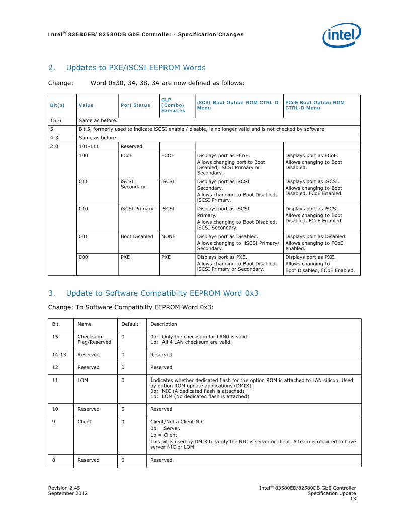
2. Updates to PXE/iSCSI EEPROM Words
Change: Word 0x30, 34, 38, 3A are now defined as follows:
3. Update to Software Compatibilty EEPROM Word 0x3
Change: To Software Compatibilty EEPROM Word 0x3:
Bit(s) Value Port StatusCLP(Combo) Executes
iSCSI Boot Option ROM CTRL-D Menu
FCoE Boot Option ROM CTRL-D Menu
15:6 Same as before.
5 Bit 5, formerly used to indicate iSCSI enable / disable, is no longer valid and is not checked by software.
4:3 Same as before.
2:0 101-111 Reserved
100 FCoE FCOE Displays port as FCoE.Allows changing port to Boot Disabled, iSCSI Primary or Secondary.
Displays port as FCoE.Allows changing to Boot Disabled.
011 iSCSI Secondary
iSCSI Displays port as iSCSISecondary.Allows changing to Boot Disabled, iSCSI Primary.
Displays port as iSCSI.Allows changing to Boot Disabled, FCoE Enabled.
010 iSCSI Primary iSCSI Displays port as iSCSIPrimary.Allows changing to Boot Disabled, iSCSI Secondary.
Displays port as iSCSI.Allows changing to Boot Disabled, FCoE Enabled.
001 Boot Disabled NONE Displays port as Disabled.Allows changing to iSCSI Primary/Secondary.
Displays port as Disabled.Allows changing to FCoE enabled.
000 PXE PXE Displays port as PXE.Allows changing to Boot Disabled, iSCSI Primary or Secondary.
Displays port as PXE.Allows changing toBoot Disabled, FCoE Enabled.
Bit Name Default Description
15 Checksum Flag/Reserved
0 0b: Only the checksum for LAN0 is valid 1b: All 4 LAN checksum are valid.
14:13 Reserved 0 Reserved
12 Reserved 0 Reserved
11 LOM 0 Indicates whether dedicated flash for the option ROM is attached to LAN silicon. Used by option ROM update applications (DMIX). 0b: NIC (A dedicated flash is attached) 1b: LOM (No dedicated flash is attached)
10 Reserved 0 Reserved
9 Client 0 Client/Not a Client NIC 0b = Server. 1b = Client. This bit is used by DMIX to verify the NIC is server or client. A team is required to have server NIC or LOM.
8 Reserved 0 Reserved.
Specification Changes - Intel® 83580EB/82580DB GbE Controller
Intel® 83580EB/82580DB GbE Controller Revision 2.45Specification Update September 201214
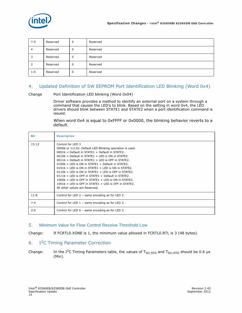
4. Updated Definition of SW EEPROM Port Identification LED Blinking (Word 0x4)
Change Port Identification LED blinking (Word 0x04)
Driver software provides a method to identify an external port on a system through a command that causes the LED's to blink. Based on the setting in word 0x4, the LED drivers should blink between STATE1 and STATE2 when a port identification command is issued.
When word 0x4 is equal to 0xFFFF or 0x0000, the blinking behavior reverts to a default.
5. Minimum Value for Flow Control Receive Threshold Low
Change: If FCRTL0.XONE is 1, the minimum value allowed in FCRTL0.RTL is 3 (48 bytes).
6. I2C Timing Parameter Correction
Change: In the I2C Timing Parameters table, the values of TSU:STA and TSU:STO should be 0.6 μs (Min).
7:5 Reserved 0 Reserved
4 Reserved 0 Reserved
3 Reserved 0 Reserved
2 Reserved 0 Reserved
1:0 Reserved 0 Reserved
Bit Description
15:12 Control for LED 3 0000b or 1111b: Default LED Blinking operation is used. 0001b = Default in STATE1 + Default in STATE2. 0010b = Default in STATE1 + LED is ON in STATE2. 0011b = Default in STATE1 + LED is OFF in STATE2. 0100b = LED is ON in STATE1 + Default in STATE2. 0101b = LED is ON in STATE1 + LED is ON in STATE2. 0110b = LED is ON in STATE1 + LED is OFF in STATE2. 0111b = LED is OFF in STATE1 + Default in STATE2. 1000b = LED is OFF in STATE1 + LED is ON in STATE2. 1001b = LED is OFF in STATE1 + LED is OFF in STATE2. All other values are Reserved.
11:8 Control for LED 2 – same encoding as for LED 3.
7:4 Control for LED 1 – same encoding as for LED 3.
3:0 Control for LED 0 – same encoding as for LED 3.
Intel® 83580EB/82580DB GbE Controller - Errata
Revision 2.45 Intel® 83580EB/82580DB GbE ControllerSeptember 2012 Specification Update
15
1.5.4 Errata
1. TAG Not Reset by Power-on-reset Function
Note: Not applicable to current products.
Status: Closed
2. MNG Reset Clears Resource Grant With No Feedback
Problem: When accessing the EEPROM (via EEC register) or FLASH (via FLA register), grants may be lost due to deadlock or FW reset. Software will not be notified of the lost grant. A driver in the middle of a bit bang may renew the request and receive the grant without knowing that it is actually starting a new transaction.
Implications:
1. FLA/EEC bit banging transactions may fail.
2. Long transactions may turn into different transactions than expected.
Workaround:
1. SW should not execute bit bang sequences longer than one word at a time.
2. When SW reads the EEC/FLA, it should make sure that it still has the request and grant; if not it should renew it and re-start the transaction (this does not cover all cases but reduces the possibility of a problem).
Status: A1 NoFix
3. Possible System Hang During Enable/Disable When Connecting through nVIdia* IO55 Slot
Problem: Once the link is up, when the 82580 tries to connect with the nVidia IO55 chipset, the following may occur:
• The Link layer tries to train but not all lanes work.
• The 82580EB/DB tries retraining with fewer lanes; but during retraining may loop.
• The system hangs.
Implication: The 82580 cannot reliably connect using this configuration.
Workaround: Connecting to a different port on the system.
Status: A1 NoFix
4. SMBus: EEPROM Not Written On ARP If the EEPROM Semaphore Is Taken by SW
Problem: If an SMBus ARP address is stored at the same time the EEPROM is locked by SW, the address is not be saved.
Implication : Wrong SMBus address after firmware reset.
Workaround: Set the SMBus address in the EEPROM (not through ARP).
Errata - Intel® 83580EB/82580DB GbE Controller
Intel® 83580EB/82580DB GbE Controller Revision 2.45Specification Update September 201216
Status: A1 NoFix
5. PCIe Links at x1 Instead of x4 When Attached to Certain Chipset Ports
Problem: When the 82580 is connected to certain PCIe x4 ports, the PCIe link is x1 instead of x4. The affected ports on Intel devices have a Device ID of 0x2690. These ports can be found on:
• 6311ESB2/6321ESB2 I/O Controller Hub
• INTEL 3100 SCH Port B
Implications: If the PCIe link is x1, the bandwidth is limited and might not be sufficient for all device ports, resulting in a performance bottleneck.
Workaround: Do not attach the 82580 to this chipset port. If such a connection cannot be avoided, please contact your Intel representative for assistance.
Status: A1 NoFix
6. LAN_DIS_N and AUX_PWR Pins Are Driven by the 82580 When Not Used for Strapping
Problem: At other times, these pins become outputs and are driven low.
Implication If these pins are driven high from another device, there could be high current draw.
If the external pull-up resistor used on these pins is not strong enough, the wrong value could be sampled at the beginning of the PCIe reset.
Workaround When driving the LANx_DIS_N and/or AUX_PWR pins from another device, use a series resistor between the devices to reduce the current.
For both external pull-up resistors and series resistors, ensure that the resistor is strong enough to pull up the pin within 40 ns. Assuming relatively short traces between the 82580 and the resistor, a 3.3 K ohm resistor should work well. Larger resistance values should not be used.
Status: A1 NoFix
7. MDIO: Com_MDIO and Destination Bits of MDICNFG Register Are Not Loaded Consistently from EEPROM
Problem: The Com_MDIO (bit 30) and Destination (bit 31) bits of the MDICNFG register (0x0E04) are not loaded consistently from the EEPROM. In some cases, the hardware default value of 0b is used instead.
Implication Software that relies on the EEPROM-loaded value might not be able to initialize an external PHY. When not using an external PHY, there is no issue.
Workaround Software should assume that the initial values of these bits are undefined and should program them before attempting to initialize an external PHY. The EEPROM bits can be used to determine the intended settings.
Intel® 83580EB/82580DB GbE Controller - Errata
Revision 2.45 Intel® 83580EB/82580DB GbE ControllerSeptember 2012 Specification Update
17
Status: A1 NoFix
8. Dummy Function Present When All Ports are Disabled
Problem: When all ports are disabled, either by strapping pins or by EEPROM settings, no PCIe functions should be present. However, if the Dummy Function Enable EEPROM bit (word 0x1B, bit 14) is set to 1b, Function 0 becomes a dummy function even if all ports are disabled.
Implication Even with all ports disabled, Function 0 appears in the system PCIe enumeration with a Device ID of 0x10A6, indicating a dummy function. This should not have any effect on the system.
Workaround N/A
Status: A1 NoFix
9. PCIe: Link Control 2 Register Contains Incorrect Read Values
Problem: The Target Link Speed and Transmit Margin fields of the Link Control 2 Register in the PCIe configuration space are described as follows in the PCIe specification:
“For a Multi-Function device associated with an Upstream Port, the field in Function 0 is of type RWS, and only Function 0 controls the component’s Link behavior. In all other Functions of that device, this field is of type RsvdP.”
This means that when reading the Link Control 2 Register on functions other than Function 0, these fields should be 0b. Instead, the 82580 returns the value written to Function 0, behavior which differs from the specification.
Implication: No functional implication since these fields are defined as reserved and ignored by software.
Workaround:N/A
Status: A1 NoFix
10. I2C Data Out Hold Time Violation
Problem: The 82580 should provide a data out hold time of 50 ns on the SFPx_I2C_DATA pins. The actual hold time is about 16 ns.
Implication: Timing specification violation. There have been no reports of failures resulting from this timing. Note that the data input hold time required is zero, so the provided output hold time should be more than enough as long as the I2C CLK and DATA signals are reasonably matched on the board.
Workaround:N/A
Status: A1 NoFix
11. SGMII: Counters Incorrectly Increment on Collision
Problem: In SGMII mode/half duplex, the statistics counters listed below incorrectly increment when a collision occurs:
Name Definition Location
RLEC Length error counter 0X4040
Errata - Intel® 83580EB/82580DB GbE Controller
Intel® 83580EB/82580DB GbE Controller Revision 2.45Specification Update September 201218
CRCERRS CRC error counter 0x4000RFC receive frame counter 0x40A8
Implication: Error counters may not be accurate.
Workaround: None.
Status: A1 NoFix
12. PCIe: Correctable Errors Reported When Using Rx L0s in a x1 Configuration
Problem: When using Rx L0s in an x1 configuration, the 82580 reports receiver errors at a rate of more than one per minute on some platforms.
Implication: Correctable errors are reported at a higher rate than can be explained by random bit errors. These errors should be ignored by the system.
Workaround: None.
Status: A1 NoFix
13. TSYNC: Auxiliary Timestamp from SDP is Unreliable
Problem: The SDP inputs to the timestamp logic are not properly synchronized. As a result, both the Auxiliary Timestamp Register values and the Auxiliary Timestamp Taken bits in TSAUXC are sometimes loaded incorrectly.
Implication: The auxiliary timestamp feature should be considered unreliable.
Workaround: For applications that use the auxiliary timestamp feature to synchronize to an external clock, it might be acceptable to drop some of the samples. For such applications, software can filter out many of the incorrect timestamp values by comparing them to an approximate expected timestamp and discarding unreasonable values.
In addition, the following method can be used to filter out incorrect values:
• Connect the input signal to two SDP inputs for the same port.
• Using the TSSDP register, assign one of the SDP inputs to AUX0 and the other SDP input to AUX1.
• When reading the TSAUXC register to check for new samples, check that both AUTT0 and AUTT1 are set. Otherwise, discard the sample.
• Read both the AUX0 and AUX1 timestamp values and compare the values. Discard the values if they differ by more than the sampling uncertainty -- 8 ns if the SDP inputs are balanced externally or slightly higher if the external trace lengths differ significantly.
Using this method, along with a SW filter for expected values, almost all errors can be filtered out, with the remaining samples having a very high probability of being correct.
When using Port 0, the following combinations of SDP connections to AUX0 and AUX1 allow the above method to filter out all errors.
AUX0 AUX1Connection Connection
SDP0 SDP1 SDP0 SDP3 SDP1 SDP0 SDP1 SDP2 SDP2 SDP0 SDP2 SDP1
Intel® 83580EB/82580DB GbE Controller - Errata
Revision 2.45 Intel® 83580EB/82580DB GbE ControllerSeptember 2012 Specification Update
19
SDP2 SDP3 SDP3 SDP2
Status: A1 NoFix
14. PCIe: N_FTS Value is too Small When Common Clock Configuration is Zero
Problem: When the Common Clock Configuration bit in the Link Control Register is 0b, the value of N_FTS advertised by the 82580 is taken from internal configuration registers, with separate values used for Gen1 and Gen2 speeds. The hardware default values are too small to guarantee a clean exit from L0s in all cases.
As a result, link recovery procedures might be performed and Correctable Errors might be reported: Bad TLP, Bad DLLP, and Replay Timer Timeout.
Note that even on platforms where the Common Clock Configuration is set to 1b, this bit is cleared by Hot Reset or D3->D0 transitions, and the previous situation can still occur until the configuration space programming has been restored.
Implications: The Correctable Errors can generally be ignored. The link recovery procedures and replayed packets result in a small reduction of effective bandwidth on the PCIe link.
However, in certain circumstances on some platforms, the repeated loss of packets can lead to a Completion Timeout error, which might cause the application and/or the system to stop working.
Workaround: Disable L0s on the upstream device.
OR
Disable L0s on the upstream device before putting the 82580 in Hot Reset or D3 states.
OR
Upgrade EEPROM image. Fix in EEPROM version 3.29. Contact your Intel represenative to obtain updated EEPROM images.
Status: A1 NoFix
15. NC-SI: Command Interface Non-functional During PCIe Reset Due to Device Power Down State
Problem: When the conditions for the Device Power Down State exist during power-up and NC-SI manageability is enabled, the MNG firmware is unable to respond to commands during PCIe reset.
This occurs when all the following are true:
• Power Down Enable EEPROM bit (word 0x1E bit 15) is set.
• PHY Power Down Enable EEPROM bit (offset 0x0F bit 6) is set for all ports using a copper link.
• SerDes Low Power Enable EEPROM bit (offset 0x0F bit 2) is set for all ports using a SerDes link.
• APM Enable EEPROM bit (offset 0x24 bit 10) is clear for all ports.
Implication: The NC-SI interface is non-functional during PCIe reset. Once PCIe reset has been negated and a Clear Initial State command has been executed, the interface functions as expected even if PCIe reset is asserted again.
Errata - Intel® 83580EB/82580DB GbE Controller
Intel® 83580EB/82580DB GbE Controller Revision 2.45Specification Update September 201220
Workaround: If the DEV_OFF_N input pin is not being used and if manageability is enabled, the Power Down Enable EEPROM bit (word 0x1E, bit 15) should be 0.
If the DEV_OFF_N input pin needs to be functional in the design, do not use the combination of EEPROM settings described above that causes this condition. For example, clear the PHY Power Down Enable bit on at least one port if using an NC-SI image.
Status: A1 NoFix
16. IEEE Std 802.3™-2008 Tx Distortion Marginality
Problem: The 82580 might not meet the IEEE Std 802.3™-2008 specification (40.6.1.2.4) that states that the Tx Distortion must meet the following criteria. “A PHY is considered to pass this test if the peak distortion is below 10 mV for at least 60% of the UI within the eye opening.” The 82580 might marginally fail this requirement.
Implication: IEEE conformance is marginal.
The Tx distortion is less than 10 mV during the critical time when the signal is actually sampled therefore no impact on system performance is observed with the 82580 due to this marginality.
Workaround: None
Status: A1 NoFix
17. NC-SI: Get NC-SI Pass-through Statistics Response Format
Problem: The NC-SI Specification, version 1.0.0a defines the Pass-through Tx Packets counter contained in the Get NC-SI Pass-through Statistics Response Packet to be an 8-byte field. The 82580 provides this counter as a 4-byte field.
Implication: A BMC that uses the Get NC-SI Pass-through Statistics command and expects the response format as described in the NC-SI Specification will not parse the response as intended by the 82580 and will obtain inaccurate statistics.
Workaround: The BMC can account for the different format provided by the 82580 and parse the response accordingly.
Status: A1 NoFix
18. PCIe Reset Causes FW Reset When Ports Are Disabled
Problem: If one or more of the ports are disabled by strapping (asserting LANx_DIS_N) or from the EEPROM (by setting the LAN_DIS bit offset 0x20, bit 11), the firmware is reset following a PCIe reset. This applies to the 82580DB (dual-port) device even if neither port is explicitly disabled.
Implication: The manageability configuration is cleared by the PCIe reset and therefore any active session is disconnected.
On some of the ports the PHY is not configured correctly following the negation of the PCIe reset until the driver is loaded and resets the PHY. An incorrectly configured PHY could cause link issues and prevent WoL and/or manageability pass-through from working during this period of time.
Workaround: The Management Controller should re-run the initialization following PCIe reset to restore the configuration.
Intel® 83580EB/82580DB GbE Controller - Software Clarifications
Revision 2.45 Intel® 83580EB/82580DB GbE ControllerSeptember 2012 Specification Update
21
No workaround is available for the PHY configuration issues; the EEPROM should be updated to avoid this issue.
Status: Fixed in EEPROM
Fixed in EEPROM version 3.29. Contact your Intel representative to obtain updated EEPROM images.
1.5.5 Software Clarifications
Applies to Intel drivers, EEPROM loads.
1. While In TCP Segmentation Offload, Each Buffer is Limited to 64 KB
Clarification: The 82580 supports 256 KB TCP packets; however, each buffer is limited to 64 KB since the data length field in the transmit descriptor is only 16 bits. This restriction increases driver implementation complexity if the operating system passes down a scatter/gather element greater than 64KB in length. This can be avoided by limiting the offload size to 64 KB.
Investigation has concluded that the increase in data transfer size does not provide any noticeable improvements in LAN performance. As a result, Intel network software drivers limit the data transfer size in all drivers to 64 KB.
Please note that Linux operating systems only support 64 KB data transfers.
For further details about how Intel network software drivers address this issue, refer to Technical Advisory TA-191.
2. EEPROM Checksum Not Set for LAN1, 2, 3
Clarification: Intel provides tools to change EEPROM content: EEUPDATE, LANCONF, and CELO. Prior to SW Release 15.7, these tools changed EEPROM content but did not update or program the EEPROM checksums for LAN1, LAN2, and LAN3. More recent Intel EEPROM tools releases (Release 15.7 and later) fix this issue; they update and set EEPROM checksums for LAN 0,1,2,3.
The more recent tools also set word 0x3 (bit 15) in the EEPROM. This setting indicates that all four EEPROM checksums are valid. If bit 15 is not set, only the LAN 0 checksum is valid.
Note: Word 0x3 (bit 15) in the EEPROM was previously RESERVED in the documentation. The bit is now used for the above purpose and is no longer RESERVED.
3. Serial Interfaces Programmed By Bit Banging
Clarification: When bit-banging on a serial interface (such as SPI, I2C, or MDIO), it is often necessary to perform consecutive register writes with a minimum delay between them. However, simply inserting a software delay between the writes can be unreliable due to hardware delays on the CPU and PCIe interfaces. The delay at the final hardware interface might be less than intended if the first write is delayed by hardware more than the second write. To prevent such problems, a register read should be inserted between the first register write and the software delay, i.e. “write”, “read”, “software delay”, “write”.
§ §
Software Clarifications - Intel® 83580EB/82580DB GbE Controller
Intel® 83580EB/82580DB GbE Controller Revision 2.45Specification Update September 201222
NOTE: This page intentionally left blank.