Embed Size (px)
Citation preview

Inside you’ll find the following papers:
This issue of Intel Technology Journal (Volume 8, Issue 3) examines the technologies and standards for WiMAX (Worldwide Interoperability for Microwave Access)—an evolving standard for point-to-multipoint wireless networking—and Intel's research and development efforts in these areas.
Intel®
TechnologyJournal
WiMAX
Volume 08 Issue 03 Published, August 20, 2004 ISSN 1535-864X
Global, InteroperableBroadband Wireless
Networks: Extending WiMAXTechnology to Mobility
RF System and CircuitChallenges for WiMAX
Scalable OFDMA PhysicalLayer in IEEE 802.16
WirelessMAN
IEEE 802.16 Medium Access Control and Service Provisioning
Multiple-Antenna Technology in WiMAX Systems
Fully Integrated CMOS Radios from RF to Millimeter
Wave Frequencies
More information, including current and past issues of Intel Technology Journal, can be found at: http://developer.intel.com/technology/itj/index.htm

Articles
Preface iii
Foreword v
Technical Reviewers vii
Global, Interoperable Broadband Wireless Networks: 173Extending WiMAX Technology to Mobility
RF System and Circuit Challenges for WiMAX 189
Scalable OFDMA Physical Layer in IEEE 802.16 WirelessMAN 201
IEEE 802.16 Medium Access Control and Service Provisioning 213
Multiple-Antenna Technology in WiMAX Systems 229
Fully Integrated CMOS Radios from RF to Millimeter Wave Frequencies 241
Volume 08 Issue 03 Published, August 20, 2004 ISSN 1535-864X
Intel® Technology Journal
WiMAX
WiMAX i

Intel Technology Journal, Volume 8, Issue 3, 2004
WiMAX ii
THIS PAGE INTENTIONALLY LEFT BLANK

Intel Technology Journal, Volume 8, Issue 3, 2004
WiMAX iii
Preface
By Lin Chao
Publisher, Intel Technology Journal WiMAX is a technology for “wireless” broadband. Today, when you want broadband, you connect using T1, DSL or cable modems to physical cables called landlines. WiMAX (Worldwide Interoperability for Microwave Access), an evolving standard for point-to-multipoint wireless networking, works for the “last mile” in the same way that Wi-Fi “hotspots” work for the last one hundred feet of networking within a building or a home. In addition to “last mile” broadband connections, WiMAX has a number of other applications in hotspots, cellular backhaul and in high-speed enterprise connectivity.
Generally speaking, WiMAX has a range of up to 30 miles. WiMAX covers several different frequency ranges. The base 802.16 standard is for the 10 to 66 GHz range. 802.16a added coverage for the 2 to 11 GHz range. WiMAX, and most commercial interests, cover these lower ranges.
The ability to provide these broadband connections wirelessly, without laying wire or cable in the ground, greatly lowers the cost to provide these services. So, WiMAX may change the economics for any place where the cost of laying or upgrading landlines to broadband capacity is prohibitively expensive, as in emerging countries. In countries like India, Mexico, and China, where there is currently insufficient wired infrastructure, WiMAX can become part of the broadband backbone.
This issue of Intel Technology Journal (Volume 8, Issue 3) examines the technologies and standards for WiMAX, and Intel’s research and development efforts in these areas. The first paper is an overview and examines Intel’s architecture vision for 802.16 and the Worldwide Interoperability Microwave Access (WiMAX) certification process. It also covers the three stages of deployments that Intel sees. The second paper discusses several RF and circuit challenges for WiMAX. WiMAX’s RF is made more complicated by the fact that WiMAX covers both licensed and unlicensed bands.
The third paper provides a brief tutorial on the IEEE 802.16 WirelessMAN Orthogonal Frequency Division Multiple Access (OFDMA) with an emphasis on a scalable OFDMA. OFDM is a spread-spectrum technology that bundles data over narrowband carriers transmitted in parallel at different frequencies. The fourth paper discusses the IEEE 802.16 Medium Access Control (MAC) protocols, which are key elements for WiMAX deployments. The fifth paper discusses the benefits of multiple antenna systems over single antenna systems in WiMAX deployments. Currently, IEEE 802.16 supports several multiple-antenna options, including Space-Time Codes (STC), Multiple-Input Multiple-Output (MIMO) antenna systems and Adaptive Antenna Systems (AAS).
The last paper explores fully integrated CMOS radios from RF to millimeter wave frequencies. The paper discusses recent CMOS with capabilities for Radio Frequency (RF), microwave, and millimeter wave circuits from 1 GHz to 100 GHz, advances in on-die isolation structures for integrating radio's delicate circuits with noisy processors, and novel design methods for complex RF passive networks on the substrate of the package.

Intel Technology Journal, Volume 8, Issue 3, 2004
WiMAX iv
These papers reveal the collective efforts by Intel, standards bodies, and the wireless industry to make WIMAX technology deployment a reality for practical applications in our everyday life.

Intel Technology Journal, Volume 8, Issue 3, 2004
WiMAX v
Foreword
Emerging Broadband Networks: The Case for WiMAX
By Scott G. Richardson Broadband Wireless Division, Intel Corporation
Broadband wireless will revolutionize people's lives by enabling a high-speed connection directly to the information they need, whenever and wherever they need it. Broadband data services, such as delivery of rich Internet Protocol and media content, are an increasingly important component of the services and revenue of network operators, who want to expand the reach of their broadband data networks without expensive construction and infrastructure costs. High-speed broadband wireless data overlays to voice network are just emerging, as service providers respond to these consumer and enterprise demands for rich media, mobile applications and services.
Intel is, and will continue to be, a key player in this broadband wireless wave, offering silicon products, platform solutions and helping to drive and develop the industry ecosystem. Intel believes multiple wireless technologies will coexist, working synergistically where the user will be “best connected” with the technology most suited to network conditions and desired services. This issue of Intel Technology Journal (ITJ) delves deeply into one of these key wireless technologies – WiMAX.
WiMAX (Worldwide Interoperability for Microwave Access) is poised to become a key technical underpinning of fixed, portable and mobile data networks. WiMAX is an implementation of the emerging IEEE 802.16 standard that uses Orthogonal Frequency Division Multiplexing (OFDM) for optimization of wireless data services. OFDM technology uses “sub-carrier optimization,” assigning small sub-carriers (kHz) to users based on radio frequency conditions. This enhanced spectral efficiency is a great benefit to OFDM networks and makes them very well suited to high-speed data connections for both fixed and mobile users. Systems based on the emerging IEEE 802.16 standards are the only standardized OFDM-based Wireless Wide Area Networks (WWAN) infrastructure platforms today.
Service providers will operate WiMAX on licensed and unlicensed frequencies. The technology enables long-distance wireless connections with speeds up to 75 megabits per second. (However, network planning assumes a WiMAX base station installation will cover the same area as cellular base stations do today.) Wireless WANs based on WiMAX technology cover a much greater distance than Wireless Local Area Networks (WLAN), connecting buildings to one another over a broad geographic area. WiMAX can be used for a number of applications, including "last-mile" broadband connections, hotspot and cellular backhaul, and high-speed enterprise connectivity for businesses.
Intel sees WiMAX deploying in three phases: the first phase of WiMAX technology (based on IEEE 802.16-2004) will provide fixed wireless connections via outdoor antennas in the first half of 2005. Outdoor fixed wireless can be used for high-throughput enterprise connections (T1/E1 class services), hotspot and cellular network backhaul, and premium residential services. In the second half of 2005, WiMAX will be available for indoor installation, with smaller antennas similar to 802.11-based WLAN access points today. In this fixed indoor model, WiMAX will be
Intel Technology Journal, Volume 8, Issue 3, 2004
WiMAX vi
available for use in wide consumer residential broadband deployments, as these devices become "user installable," lowering installation costs for carriers.
By 2006, technology based on the IEEE 802.16e standards will be integrated into portable computers to support movement between WiMAX service areas. This allows for portable and mobile applications and services. In the future, WiMAX capabilities will even be integrated into mobile handsets.
In this issue of the Intel Technology Journal, we give background into the key silicon and system design issues for WiMAX networks, including radio frequency, physical layer and media access control technologies. We also discuss network-level architecture for WiMAX and how to create end-to-end, interoperable networks based on a common set of protocols and standards. In addition, Intel Technology Journal pays particular attention to issues of silicon integration and managing multiple antennas, very important in an environment where cost/power are paramount and users will use multiple wireless technologies to access the network. With the background provided in this issue of the ITJ, the reader will be better informed of the exciting benefits of this new standard and technology, and will be better able to profit from this new wireless wave.
Intel Technology Journal, Volume 8, Issue 3, 2004
WiMAX vii
Technical Reviewers
Alluri, Prasad, Intel Communications Group Andelman, Dov, Intel Communications Group
Baraa, Al-Dabagh, Intel Communications Group Cox, Timothy F., Intel Communications Group
Foerster, Jeffrey R., Corporate Technology Group Ho, Minnie, Corporate Technology Group
Kalluri, Sudhakar, Desktop Platforms Group Lebizay, Gerald, Intel Communications Group
Liu, Tony, Intel Communications Group Mitchel, Henry, Intel Communications Group Ovadia, Shlomo, Intel Communications Group Putzolu, David, Intel Communications Group
Salvekar, Atul A., Intel Communications Group Talwar, Shilpa, Corporate Technology Group Teckman, Tim, Intel Communications Group Thomas, Rainer E., Desktop Platforms Group
Intel Technology Journal, Volume 8, Issue 3, 2004
WiMAX viii
THIS PAGE INTENTIONALLY LEFT BLANK

Global, Interoperable Broadband Wireless Networks: Extending WiMAX Technology to Mobility 173
Global, Interoperable Broadband Wireless Networks: Extending WiMAX Technology to Mobility
Ed Agis, Intel Communications Group, Intel Corporation Henry Mitchel, Intel Communications Group, Intel Corporation Shlomo Ovadia, Intel Communications Group, Intel Corporation
Selim Aissi, Corporate Technology Group, Intel Corporation Sanjay Bakshi, Corporate Technology Group, Intel Corporation Prakash Iyer, Corporate Technology Group, Intel Corporation
Masud Kibria, Corporate Technology Group, Intel Corporation Christopher Rogers, Corporate Technology Group, Intel Corporation
James Tsai, Corporate Technology Group, Intel Corporation
Index words: 802.16, WiMAX, OFDM, OFDMA, portability, mobility, broadband wireless architecture, PKM, WiMAX certification, interoperability
ABSTRACT
IEEE* 802.16 is an emerging global broadband wireless access standard capable of delivering multiple megabits of shared data throughput supporting fixed, portable, and mobile operation. The standard offers a great deal of design flexibility including support for licensed and license-exempt frequency bands, channel widths ranging from 1.25 to 20 MHz, Quality of Service (QoS) establishment on a per-connection basis, strong security primitives, multicast support, and low latency/low packet loss handovers1. Mass deployments of Subscriber Stations (SS) and Access Points2 (AP) for portable and mobile services are expected to be based on scalable Orthogonal Frequency Division Multiplexing with Multiple Access (OFDMA). A broad range of network operators are anticipated to deploy such systems in licensed frequencies below 11 GHz. However, universal acceptance of 802.16 for portable and mobile use is contingent on the Industry’s development, acceptance,
*Other brands and names are the property of their respective owners 1 Optimization of PHY and MAC handover primitives is ongoing in the 802.16e Task Group and is expected to be completed by the end of 2004. 2 In this paper the term Access Point is synonymous with Base Station, and an AP can be logically broken into a combination of one APC and one or more APTs.
and conformance to two complementary aspects of the IEEE 802.16 air interface standards work: (1) development and adoption of an open and extensible end-to-end architecture framework and specification that is agnostic to incumbent operator backend networks; and (2) a means for ensuring spec-compliant and vendor interoperable equipment to support cost-effective deployments and give users the capability to roam across networks established by different network operators. A common architecture framework and standardized compliance testing mechanisms based on a suite of PHY and MAC profiles will enable multivendor interoperability supporting different deployment and use-case scenarios. In this paper, we describe Intel’s 802.16 architecture vision and the Worldwide Interoperability Microwave Access (WiMAX) certification process to address these two important market needs.
INTRODUCTION IEEE 802.16 is an emerging suite of air interface standards for combined fixed, portable, and Mobile Broadband Wireless Access (MBWA). Initially conceived as a radio standard to enable cost-effective last-mile broadband connectivity to those not served by wired broadband such as cable or DSL, the specifications are evolving to target a broader market opportunity for mobile, high-speed broadband applications. The promise of realizing a low-cost, broadly interoperable wide-area data network that supports portable and mobile usage

Intel Technology Journal, Volume 8, Issue 3, 2004
Global, Interoperable Broadband Wireless Networks: Extending WiMAX Technology to Mobility 174
could have significant end-user benefits. Notably, this network can complement and extend the Wi-Fi hotspot usage model to provide broader Internet Protocol (IP) data service coverage and roaming that has so far eluded current 3G systems, due to system cost and complexity.
The 802.16-2004 [1] standard to be published later this year supersedes all previous versions as the base standard and specifies networks for the current fixed access market segment. The 802.16e [2] amendment and the soon to be approved 802.16f and 802.16g task groups will amend the base specification to enable not just fixed, but also portable and mobile operation in frequency bands below 6 GHz.
802.16 is optimized to deliver high, bursty data rates to Subscriber Stations (SS) but the sophisticated Medium Access Control (MAC) architecture can simultaneously support real-time multimedia and isochronous applications such as Voice Over IP (VoIP) as well. This means that IEEE 802.16 is uniquely positioned to extend broadband wireless beyond the limits of today’s Wi-Fi systems, both in distance and in the ability to support applications requiring advanced Quality of Service (QoS) such as VoIP, streaming video, and on-line gaming.
The technology is expected to be adopted by different incumbent operator types–for example, Wireless Internet Service Providers (WISPs), cellular operators (CDMA and WCDMA), and wireline broadband providers. Each of these operators will approach the market with different business models, each based on their current markets and perceived opportunities for broadband wireless as well as different requirements for integration with existing (legacy) networks. As a result, 802.16 network deployments face the challenging task of needing to adapt to different network architectures while still supporting standardized components and interfaces for multivendor interoperability.
This paper is organized into two main sections. The first section presents Intel’s deployment vision and architecture framework for 802.16. The architecture and usage is presented as a two-stage evolution: initially combining fixed access with portability and scaling up to evolve to full mobility. The framework is based on several core principles:
• Support for different Radio Access Network (RAN) topologies.
• Well-defined interfaces to enable 802.16 RAN architecture independence while enabling seamless
integration and interworking with Wi-Fi, 3GPP3 and 3GPP2 networks.
• Leverage open, Internet Engineering Task Force (IETF)-defined IP technologies to build scalable all-IP 802.16 access networks using Common Off The Shelf (COTS) equipment.
• Support for IPv4 and IPv6 clients and application servers; recommending use of IPv6 in the infrastructure.
• Functional extensibility to support future migration to full mobility and delivery of rich broadband multimedia.
In the second section, the WiMAX certification process with its key building blocks is reviewed. The WiMAX certification process, which is being established by the WiMAX Forum, enables multivendor interoperability of subscriber systems and access points for this ecosystem.
BROADBAND WIRELESS DEPLOYMENT SCENARIOS Initial deployments of IEEE 802.16 standards-based networks will likely target fixed access connectivity to unserved and underserved markets where wireline broadband services are insufficient to fulfill the market need for high-bandwidth Internet connectivity. Pre-standards implementations exist today that are beginning to address this fixed access service environment. Standardization will help accelerate the ramp for these fixed access solutions by providing interoperability amongst equipment and economies of scale resulting from high-volume standards-based components.
As IEEE 802.16 solutions evolve to address portable and mobile applications, the required features and performance of the system will increase. Beyond fixed access service, even larger market opportunities exist for providing cost-effective broadband data services to users on the go. Initially this includes portable connectivity for customers who are not within reach of their existing fixed broadband or WLAN service options. This type of service is characterized by access that is unwired but stationary in most cases, albeit with some limited provisions for user mobility during the connection. In this manner, 802.16 can be seen as augmenting coverage of 802.11 for private and public service networks and cost effectively extending hotspot availability to wider ranges of
3 3GPP – Third Generation Partnership Project – a collaborative effort between ARIB, CCSA, ETSI, ATIS, TTA, and TTC to develop 3G telecommunications standards. 3GPP2 is a similar collaborative effort between ANSI, TIA and EIA-41.
Intel Technology Journal, Volume 8, Issue 3, 2004
Global, Interoperable Broadband Wireless Networks: Extending WiMAX Technology to Mobility 175
coverage. Based on this described capability, this phase of deployment is referred to as “Portability with Simple Mobility.”
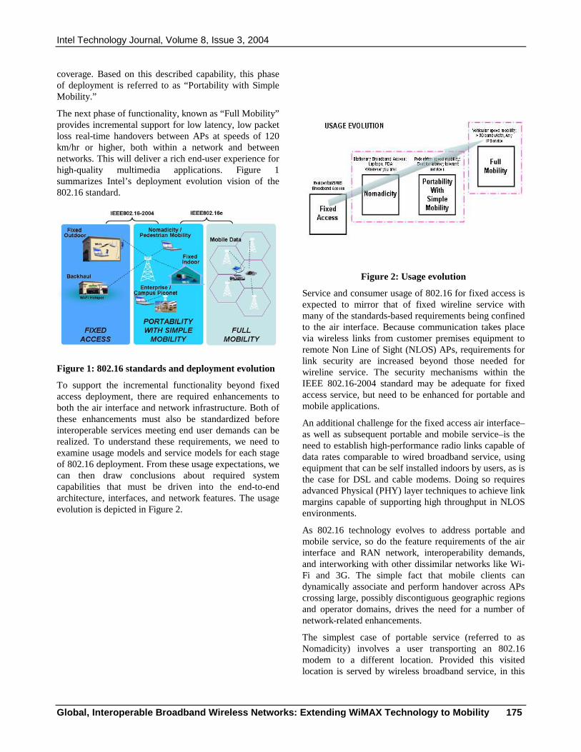
The next phase of functionality, known as “Full Mobility” provides incremental support for low latency, low packet loss real-time handovers between APs at speeds of 120 km/hr or higher, both within a network and between networks. This will deliver a rich end-user experience for high-quality multimedia applications. Figure 1 summarizes Intel’s deployment evolution vision of the 802.16 standard.
Figure 1: 802.16 standards and deployment evolution
To support the incremental functionality beyond fixed access deployment, there are required enhancements to both the air interface and network infrastructure. Both of these enhancements must also be standardized before interoperable services meeting end user demands can be realized. To understand these requirements, we need to examine usage models and service models for each stage of 802.16 deployment. From these usage expectations, we can then draw conclusions about required system capabilities that must be driven into the end-to-end architecture, interfaces, and network features. The usage evolution is depicted in Figure 2.
Figure 2: Usage evolution
Service and consumer usage of 802.16 for fixed access is expected to mirror that of fixed wireline service with many of the standards-based requirements being confined to the air interface. Because communication takes place via wireless links from customer premises equipment to remote Non Line of Sight (NLOS) APs, requirements for link security are increased beyond those needed for wireline service. The security mechanisms within the IEEE 802.16-2004 standard may be adequate for fixed access service, but need to be enhanced for portable and mobile applications.
An additional challenge for the fixed access air interface–as well as subsequent portable and mobile service–is the need to establish high-performance radio links capable of data rates comparable to wired broadband service, using equipment that can be self installed indoors by users, as is the case for DSL and cable modems. Doing so requires advanced Physical (PHY) layer techniques to achieve link margins capable of supporting high throughput in NLOS environments.
As 802.16 technology evolves to address portable and mobile service, so do the feature requirements of the air interface and RAN network, interoperability demands, and interworking with other dissimilar networks like Wi-Fi and 3G. The simple fact that mobile clients can dynamically associate and perform handover across APs crossing large, possibly discontiguous geographic regions and operator domains, drives the need for a number of network-related enhancements.
The simplest case of portable service (referred to as Nomadicity) involves a user transporting an 802.16 modem to a different location. Provided this visited location is served by wireless broadband service, in this
Intel Technology Journal, Volume 8, Issue 3, 2004
Global, Interoperable Broadband Wireless Networks: Extending WiMAX Technology to Mobility 176
scenario, the user re-authenticates and manually re-establishes new IP connections and is afforded broadband service at the visited location.
This usage enhancement over fixed access requires enhancements to security such as strong mutual authentication between the user/client device and the network AP supporting a flexible choice of credential types. Portable and mobile devices need a means for authenticating trusted APs and detecting rogue APs. Such mutual authentication is not present in the fixed access standard. Also a common centralized mechanism for user authentication is needed as users may move between different APs within an IP prefix or subnet, or across APs in different subnets, or even roam to other service providers in different locales.
The next stage, portability with simple mobility, describes a more automated management of IP connections with session persistence or automatic reestablishment following transitions between APs. This incremental enhancement allows for more user transparent mobility and is suitable for latency tolerant applications such as TCP [13]; it does not provide adequate handover performance for delay and packet loss sensitive real-time applications such as VoIP.
In the fully mobile scenario, user expectations for connectivity are comparable to those experienced in 3G voice/data systems. Users may be moving while simultaneously engaging in a broadband data access or multimedia streaming session. The need to support low latency and low packet loss handovers of data streams as users transition from one AP to another is clearly a challenging task. For mobile data services, users will not easily adapt their service expectations because of environmental limitations that are technically challenging but not directly relevant to the user (such as being stationary or moving). For these reasons, the network and air interface must be designed up front to anticipate these user expectations and deliver accordingly.
THE 802.16 RADIO–SCALING TO FULL MOBILITY The 802.16 standard provides an excellent framework upon which systems can be built to satisfy the broad spectrum of usage models described above. Of the three PHY layers supported in the standard, scalable OFDMA is the most versatile and the one preferred for operation across channel widths ranging from 1.75 MHz to 20 MHz. Single Carrier Access (SCa) will likely be considered for backhaul links while OFDM with 256-point Fast Fourier Transform (FFT) is best suited for Fixed Access in up to 10 MHz channel widths. Scalable OFDMA supports features (enhanced over OFDM) that
are especially suited for high-speed mobile operation such as Downlink (DL) and Uplink (UL) subchannelization, fixed subcarrier spacing (by maintaining constant ratio of FFT size to channel width), and reduced overhead for Cyclic Prefix (CP) by keeping its duration constant at 1/8th the OFDMA symbol duration.
The 802.16 MAC is designed for Point-to-Multipoint (PMP) applications and is based on Collision Sense Multiple Access with Collision Avoidance (CSMA/CA). The 802.16 AP MAC manages UL and DL resources including Transmit and Receive scheduling. The MAC incorporates several features suitable for a broad range of applications at different mobility rates, such as the following:
• Four service classes–Unsolicited Grant Service (UGS), real-time Polling Service (rtPS), non-real-time Polling Service (nrtPS), and Best Effort (BE).
• Header suppression, packing, and fragmentation for efficient use of spectrum.
• Privacy Key Management (PKM) for MAC layer security. PKM version 2 incorporates support for Extensible Authentication Protocol (EAP).
• Broadcast and Multicast support.
• Manageability primitives.
• High-speed handover and mobility management primitives.
• Three power management levels: Normal Operation, Sleep, and Idle (with paging support).
These features combined with the inherent benefits of scalable OFDMA make 802.16 suitable for high-speed data and bursty or isochronous IP multimedia applications.
REQUIREMENTS AND TENETS FOR A GLOBAL INTEROPERABLE END-TO-END ARCHITECTURE FRAMEWORK The architecture framework presented in this paper is based on the following requirements:
• Applicability: The architecture shall be applicable to licensed and license-exempt 802.16 deployments.
• Service Provider Categories: The architecture, especially the RAN, shall be suitable for adoption by all incumbent operator types, examples of which were listed earlier.

Intel Technology Journal, Volume 8, Issue 3, 2004
Global, Interoperable Broadband Wireless Networks: Extending WiMAX Technology to Mobility 177
• Harmonization/Interworking: The architecture shall lend itself to integration with an existing IP operator core network (e.g., DSL, cable, or 3G) via interfaces that are IP-based and not operator-domain specific. This permits reuse of mobile client software across operator domains.
• Provisioning and Management: The architecture shall accommodate a variety of online and offline client provisioning, enrollment, and management schemes based on open, broadly deployable Industry standards.
• IP Connectivity: The architecture shall support a mix of IPv4 and IPv6 network interconnects and communication endpoints and a variety of standard IP context management schemes.
• IP Services: The architecture shall support a broad range of TCP and UDP real-time and non-real-time applications.
• Security: The architecture shall support Subscriber Station (SS) authorization, strong bilateral user authentication based on a variety of authentication mechanisms such as username/password, X.509 certificates, Subscriber Identity Module (SIM), Universal SIM (USIM), Removable User Identity Module (RUIM), and provide services such as data integrity, data replay protection, data confidentiality, and non-repudiation using the maximum key lengths permissible under global export regulations.
• Mobility Management: The architecture shall scale from fixed access to fully mobile operation scenarios with scalable infrastructure evolution, eventually supporting low latency (< 100 msec) and virtually zero packet loss handovers at mobility speeds of 120 km/hr or higher.
• IP Connectivity: The architecture shall support a mix of IPv4 and IPv6 network interconnects and communication endpoints and a variety of standard IP context management schemes.
The architecture framework is based on the following principles:
• Extensive use of IETF standards for IP routing, AAA, QoS and traffic engineering protocols in the RAN and integration with an operator’s IP core/data center, enabling multivendor infrastructure interoperability.
• Functional decomposition that supports mixed operation and scaling up from NLOS portable operation to seamless mobility across RAN clouds spanning multiple IP subnets or prefixes.
• RAN architecture independence from an operator IP core or other interconnected networks.
• Loosely coupled interworking with 3G and Wi-Fi networks.
• An end-to-end security framework that is compatible with Wi-Fi, supporting credential reuse and similar consistent use of AAA protocols.
END-TO-END ARCHITECTURE EVOLUTION Figure 3 conceptually depicts the architecture evolution for 802.16. A basic 802.16-2004-based Fixed Access (indoor4 and outdoor) deployment is typically accomplished via a static provisioning relationship between an SS and an 802.16 AP. The collection of APs and interconnecting routers or switches comprising the RAN can be logically viewed as a contiguous cloud with no inter-AP mobility requirements from an SS perspective. The RAN(s) interconnect via a logically centralized operator IP core network to one or more external networks as shown. The operator IP core may host services such as IP address management, Domain Name Service (DNS) [12], media switching between IP packet-switched data and Public Switched Telephony Network (PSTN) circuit-switched data, 2.5G/3G/Wi-Fi harmonization and interworking, and VPN services (provider hosted or transit).
Going from Fixed access to Portability with Simple Mobility involving the use of Mobile SSs (MSS) such as laptops and Personal Device Assistants (PDA) introduces network infrastructure changes such as the need to support break-before-make micro- and macro-mobility5 handovers across APs with relaxed handover packet loss and latency6 (less than two seconds), cross-operator roaming, and the need to support reuse of user and MSS credentials across logically partitioned RAN clouds.
Going from Portability to Full Mobility requires support in the RAN for low (~zero) packet loss and low latency (<100 msec) make-before-break handovers and mechanisms such as Idle mode with paging for extended low-power operation.
4 Indoor operation may require use of Beam Forming or Multiple Input Multiple Output (MIMO) Advanced Antenna Systems (AAS) which are supported in the 802.16 standard.
5 Micro-mobility refers to handovers between APs within the same IP prefix or subnet domain. Macro-mobility refers to handovers across APs in different IP prefix or subnet domains.
6 Latency may be unacceptable for real-time IP services such as VoIP during handovers but acceptable for TCP and VPN services as well as store-and-forward multimedia services.

Intel Technology Journal, Volume 8, Issue 3, 2004
Global, Interoperable Broadband Wireless Networks: Extending WiMAX Technology to Mobility 178
An important design consideration is QoS. Fixed Access and Portable usage models need only support acceptable QoS guarantees for stationary usage scenarios. Portability introduces the requirement to transfer the Service Level Agreement (SLA) across APs involved in a handover, although QoS may be relaxed during handovers. Full Mobility requires consistent QoS in all operating modes, including handovers. The 802.16 RAN will need to deliver Bandwidth and/or QoS on Demand as needed to support diverse real-time and non-real-time services over the 802.16 RAN. Besides the traditional Best Effort forwarding, the RAN will need to handle latency intolerant traffic generated by applications such as VoIP and interactive games.
The decoupling of the RAN from an operator IP core network permits incremental migration to fully mobile operation. An operator must however give due consideration to the RAN topology (such as coverage overlap, user capacity, and range) to ensure that the physical network is future-proof for such an evolution.
Figure 3: 802.16 architecture evolution
END-TO-END REFERENCE ARCHITECTURE Figure 4 depicts an end-to-end reference architecture for 802.16. Various functional entities and interoperability interfaces are identified. The network essentially decomposes into three major functional aggregations: the 802.16 SS/MSS, the 802.16 RAN, and interconnect to various operator IP core and application provider networks. The IP core network a) manages the resources of the 802.16 RAN, and b) provides core network services such as address management, authentication, service authorization, and provisioning for 802.16 SS/MSSs.
The reference architecture, especially interconnectivity in the RAN and interconnects to remote IP networks, is based on extensive use of native IP suite of protocols that in turn can deliver desired economies of scale. In the sections below, we describe three logical entities: the Radio Network Serving Node (RNSN), AP, and SS/MSS. We also briefly describe the interoperability interfaces identified in Figure 4.
Figure 4: 802.16 reference architecture
Radio Network Serving Node (RNSN)
A Radio Network Service Node (RNSN) is a logical network entity that interfaces the RAN with the operator IP core network, Application Service Provider (ASP) networks, and other service networks such as IP Multimedia Subsystems (IMS), remote Enterprise Intranets, PSTN, and the Internet. Each RNSN instance manages a cloud of APs across a hybrid wireline/wireless backhaul network and is responsible for Radio Resource Management (RRM), data forwarding, and interconnects to back-end networks. Functions such as QoS, mobility, and security are cooperatively managed as a network of managed APs. An RNSN may also host RAN-specific centralized functions such as paging groups and macro mobility agents, an example of which is a Mobile IP (MIP) Foreign Agent (FA), and so on. An RNSN may be rendered on a convenient network infrastructure platform such as a Packet Data Gateway (PDG) [5] in 3GPP networks or a Packet Data Serving Node (PDSN) in a 3GPP2 network or on a standalone router platform.
Access Point (AP)
An 802.16 Access Point (referred to in the 802.16 standard as a base station) is a logical entity that provides the necessary over-the-air standards-compliant

Intel Technology Journal, Volume 8, Issue 3, 2004
Global, Interoperable Broadband Wireless Networks: Extending WiMAX Technology to Mobility 179
functionality including SS/MSS admission control and all RRM and UL/DL scheduling.
We envision a number of AP/RAN topologies as depicted in Figure 5.
Figure 5: 802.16 RAN topologies
An AP may form a subnet/prefix boundary as indicated by an AP Router (APR) in the figure. An AP may be implemented as an integrated MAC/PHY entity or may take on a more distributed architecture involving an AP Controller (APC) and AP Transceivers (APT) that would render cells in groups.
A combination of an APC with one or more APT instances may render a multisector cell. Where multiple APTs are managed by an APC, the APC may host a common MAC instance across all APTs or a dedicated MAC instance for each APT. An APC would typically localize all micromobility functions across its managed APTs and as such would support all relevant 802.16 PHY, MAC, and Convergence Sublayer (CS) Service Access Point (SAP) primitives. An APC may also host optional wireless link services such as header suppression, payload compression, and MSS paging.
An AP hosting more than one logical APC instance can optimize control and management plane functions across all hosted instances. Factors such as projected scalability requirements (coverage, user density), degree of mobility, and need for incremental network growth would drive an operator’s choices between the different AP configurations. However, the architecture framework is agnostic to specific RAN topologies and can support a mix of all possible variants simultaneously.
Mobile/Fixed Subscriber Station (MSS/SS) Mobile and Fixed SSs form the third most important functional aggregation in the end-to-end framework. We envision that most operator networks would, over time, have to support a mix of SSs with varying degrees of mobility support.
INTEROPERABILITY INTERFACES Figure 4 identified several key interoperability interfaces within the end-to-end framework. The functionality and purpose of each of these interfaces is discussed below. All interfaces are bi-directional unless noted otherwise.
I-SSAP and I-MSSAP This is the control, data, management and service plane interface between fixed-only or mobile SSs and 802.16 APs. The functions supported over this interface include, but are not limited to the following:
• SS/MSS connectivity provisioning and admission control
• Over-the-air and end-to-end security
• Mobility management
• Device management
• UL and DL data exchange
• Authorization and tunneling for specialized IP services
• Application layer end-to-end signaling
• Advanced functions such as power management (paging), compression, data reliability
As noted earlier, the 802.16 standard presents a rich selection of optional features that in turn presents significant interoperability challenges to the Industry. We expect the WiMAX Forum to define profiles targeting operation in specific frequency bands, channel widths, PHY modes, and duplexing modes to drive multivendor interoperability. All such applicable profiles will be incorporated in the I-SSAP and I-MSSAP interfaces.
I-CN1 and I-CN2 I-CN1 represents the control, data, and management planes between 802.16 RANs and an operator’s core network (with interfaces in turn to other remote networks). I-CN2 represents control, management, and service planes to ASP networks. Both of these interfaces are exposed by the RNSN and enable a consistent all-IP interface to diverse core networks. The functions modeled over this interface may be provided by a cluster
Intel Technology Journal, Volume 8, Issue 3, 2004
Global, Interoperable Broadband Wireless Networks: Extending WiMAX Technology to Mobility 180
of servers, for example, DHCP, DNS, IMS Core Network components such as Proxy-Call Session Control Function (P-CSCF), Interrogating-CSCF (I-CSCF), Serving-CSCF (S-CSCF), Media Gateway (MGW), and so on. These interfaces may also host IP tunnels to carry data between provider networks.
The functions supported over this interface include, but are not limited to the following:
• Assignment of traffic engineering parameters for provisioned QoS for both control and data plane traffic.
• User authentication via AAA intermediaries and servers.
• Services authorization, access control, and charging. • IP connectivity management and security (for
example, domain firewall). • Troubleshooting network access problems,
application-specific problems and RAN event handling.
• Data traffic and macro mobility management.
I-RNSN This is the control, data, and management plane interface between two RNSNs that logically may demarcate two RAN clouds. The interface typically handles inter-RNSN mobility management control and data plane traffic (including temporary data tunneling between RNSNs serving Serving and Target APs during handovers).
I-RNSNAP This is the control, data, and management plane interface between an AP (or any of its control plane variants) and an RNSN. This interface demarcates the two endpoints of the RAN across which intra-RAN micro- and macro-mobility functions are performed. The interface also supports functions such as paging.
Mobility Management The 802.16-2004 standard defines a BS as a single sector entity supporting one frequency assignment. The 802.16e amendment defines MAC message primitives to support network or MSS initiated handovers. The very basic handover scenario for a real-world multisector AP would be an inter-sector handover. The amendment defines handover optimization flags representing levels of handover context information that is shared between neighbor AP entities (sector line cards in a multisector AP or between the sector line cards in two different APs). The optimization flags consequently enable modeling of all possible handover scenarios from the most basic nomadic access scenario (where no network entry context is shared between APs across a handover) to scenarios involving inter-subnet, inter-frequency assignment, Idle
mode, and inter-physical AP handovers. Furthermore, optional advanced features such as Soft handover (with PHY layer macro diversity) and Fast Base Station Switching are being defined to support zero packet loss, low latency inter-sector handovers. The design goal for mobility management is to build on these primitives to deliver the desired handover performance. Fixed access and nomadic access require no handover support. Portability implies fast intra-RAN switching with potential data loss during handovers and even more latency and data loss during inter-subnet handovers. Full mobility requires zero/low packet loss and low latency handovers that are acceptable to real-time applications such as VoIP.
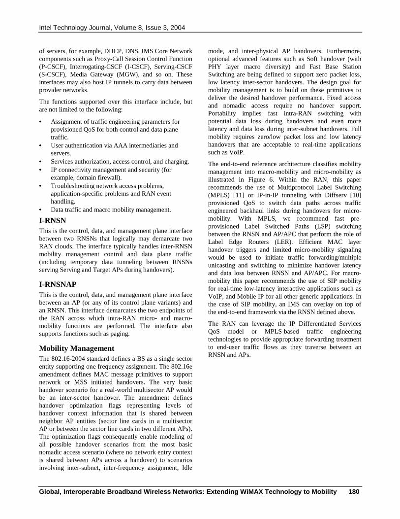
The end-to-end reference architecture classifies mobility management into macro-mobility and micro-mobility as illustrated in Figure 6. Within the RAN, this paper recommends the use of Multiprotocol Label Switching (MPLS) [11] or IP-in-IP tunneling with Diffserv [10] provisioned QoS to switch data paths across traffic engineered backhaul links during handovers for micro-mobility. With MPLS, we recommend fast pre-provisioned Label Switched Paths (LSP) switching between the RNSN and AP/APC that perform the role of Label Edge Routers (LER). Efficient MAC layer handover triggers and limited micro-mobility signaling would be used to initiate traffic forwarding/multiple unicasting and switching to minimize handover latency and data loss between RNSN and AP/APC. For macro-mobility this paper recommends the use of SIP mobility for real-time low-latency interactive applications such as VoIP, and Mobile IP for all other generic applications. In the case of SIP mobility, an IMS can overlay on top of the end-to-end framework via the RNSN defined above.
The RAN can leverage the IP Differentiated Services QoS model or MPLS-based traffic engineering technologies to provide appropriate forwarding treatment to end-user traffic flows as they traverse between an RNSN and APs.
Intel Technology Journal, Volume 8, Issue 3, 2004
Global, Interoperable Broadband Wireless Networks: Extending WiMAX Technology to Mobility 181
Figure 6: Mobility management
Harmonization and Interworking with Public Wi-Fi and 3G Networks As noted earlier, different incumbent operators are likely to deploy 802.16 networks either as a data overlay network or as a standalone broadband access network. Integration with an existing operator network would involve either harmonization or interworking as defined below.
Interworking implies a technical and business relationship between operators owning homogenous or heterogeneous networks enabling subscribers to authenticate/authorize to their home operator network via the “visited” network and utilize system functions and IP services offered by both networks.
Harmonization on the other hand is a situation where two or more homogeneous or heterogeneous networks owned by an operator are offered as an integrated network to users.
The document http://www.intel.com/technology/IWS/WLAN_study.pdf describes Intel’s proposed interworking framework for public Wi-Fi hotspots. We recommend adopting and extending the same principles for inter-operator 802.16 interworking, supporting the following goals:
• An operator type–agnostic one-bill roaming (via common, extensible RADIUS [6] and DIAMETER [7] accounting primitives) framework across 802.16 networks–eventually leading to seamless IP services mobility across these networks.
• Support reuse of credentials and cryptographically strong bilateral authentication and session key management across these networks.
• A provisioning and access framework for advanced IP services that is compatible with the architecture for Wi-Fi hotspots.
• Enable offering of multiple IP services with attributes such as provisioned bandwidths, SLAs, QoS, and variable tariff profiles.
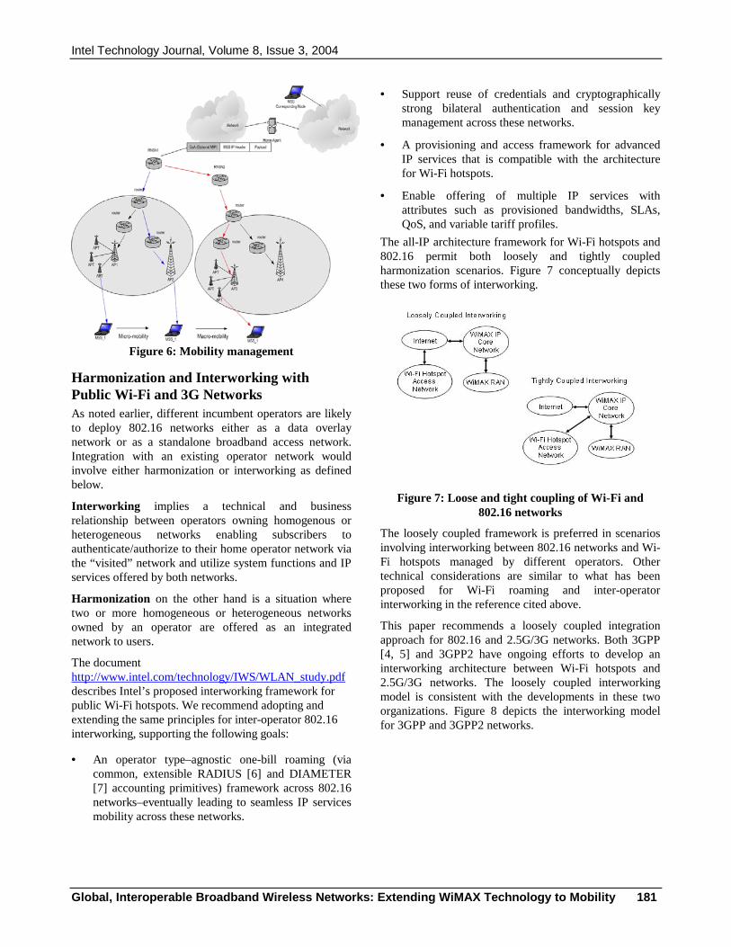
The all-IP architecture framework for Wi-Fi hotspots and 802.16 permit both loosely and tightly coupled harmonization scenarios. Figure 7 conceptually depicts these two forms of interworking.
Figure 7: Loose and tight coupling of Wi-Fi and
802.16 networks
The loosely coupled framework is preferred in scenarios involving interworking between 802.16 networks and Wi-Fi hotspots managed by different operators. Other technical considerations are similar to what has been proposed for Wi-Fi roaming and inter-operator interworking in the reference cited above.
This paper recommends a loosely coupled integration approach for 802.16 and 2.5G/3G networks. Both 3GPP [4, 5] and 3GPP2 have ongoing efforts to develop an interworking architecture between Wi-Fi hotspots and 2.5G/3G networks. The loosely coupled interworking model is consistent with the developments in these two organizations. Figure 8 depicts the interworking model for 3GPP and 3GPP2 networks.

Intel Technology Journal, Volume 8, Issue 3, 2004
Global, Interoperable Broadband Wireless Networks: Extending WiMAX Technology to Mobility 182
Figure 8: Reference model for 802.16 interworking with 2.5G/3G
3GPP has defined a Public Wi-Fi IP interworking entity called the Packet Data Gateway (PDG) to be incorporated in Release 6. With adaptations as needed based on functional requirements, the PDG can serve as the ingress to the operator IP core network (the 802.16 core network).
3GPP2 has a similar ongoing effort for Wi-Fi-3GPP2 interworking and will also identify a transport and signaling gateway that essentially supports integration of a 802.16 RAN into a 3GPP2 IP core network.
Note that while the RNSN is shown as a separate logical entity in Figure 8, most if not all of its functions on the IP core interconnect interface may be entirely subsumed by the PDG or PDSN while functions on the RAN interface may be subsumed by one or more APs.
End-to-End Security Figure 9 conceptually depicts end-to-end Authentication, Authorization, and Accounting (AAA) on 802.16 networks supporting portability and fully mobile operations. The figure borrows terminology from Wi-Fi and is built on the three-party protocol (PKM v2) foundation being defined in 802.16e.
Figure 9: 802.16 security framework
As shown in this figure, over-the-air authentication and encryption (security association) is established using the PKM-EAP protocol. Extensible Authentication Protocol (EAP) is carried over RADIUS or DIAMETER to the AAA backend. The use of EAP enables support for cryptographically strong key-deriving methods such as EAP-AKA and EAP-MSCHAPv2. Intel also recommends using an end-to-end tunneling protocol such as Protected EAP (PEAP) or Tunneled TLS (TTLS) to afford mutual authentication and 128-bit or better Transport Layer Security (TLS) encryption to further enhance end-to-end security (especially in situations where cryptographically weaker EAP methods may be deployed). The AP or APC or APR serves as the “Authenticator” and hosts a RADIUS or DIAMETER AAA client. All AAA sessions are terminated on an AAA server that may be in the operator’s IP core network or an external IP network in roaming scenarios. The RNSN is merely a conduit for the AAA messages and does not play a significant role in the AAA process. In some instances, the network may employ an AAA aggregator/intermediary but the architecture is not impacted in those cases. Additionally, the RNSN may host a firewall to filter downstream traffic to a RAN.
THE WIMAX FORUM In order for the defined IEEE 802.16 broadband wireless network architecture to become a reality, service providers must be assured that multivendor BS/SS interoperability is verified by an independent certification lab. The WiMAX Forum is a non-profit consortium of broadband wireless system vendors, service providers, component suppliers, and operators focused on enabling the development and deployment of interoperable

Intel Technology Journal, Volume 8, Issue 3, 2004
Global, Interoperable Broadband Wireless Networks: Extending WiMAX Technology to Mobility 183
broadband wireless products around the world. Today, the consortium is focused on the development of conformance, interoperability, and certification of APs and SSs for Non Line of Sight (NLOS) operation below 11 GHz based on the IEEE 802.16 standard.
Figure 10: WiMAX certification process (preliminary)
The following section is divided into two main parts. First, the WiMAX conformance and interoperability processes are explained, and the WiMAX system profiles for certification are discussed. Second, the challenges facing the WiMAX certification process, including certification lab set-up and the development of the WiMAX protocol analyzer, are discussed.
WIMAX CERTIFICATION PROCESS
Conformance vs. Interoperability WiMAX conformance should not be confused with interoperability. However, the combination of these two types of testing make up what is commonly referred to as certification testing. WiMAX conformance testing can be done by either the certification lab or another test lab and is a process where BS and SS manufacturers will be testing their pre-production or production units to ensure that they perform in accordance with the specifications called out in the WiMAX Protocol Implementation Conformance Specification (PICS) document. Based on the results of conformance testing, BS/SS vendors may choose to modify their hardware and/or firmware and formally re-submit these units for conformance testing. The conformance testing process may be subject to a vendor’s personal interpretation of the IEEE standard, but the BS/SS units must pass all mandatory and prohibited test conditions called out by the test plan for a specific system profile.
On the other hand, WiMAX interoperability is a multivendor (≥3) test process hosted by the certification
lab to test the performance of BS and/or SS from one vendor to transmit and receive data bursts from another vendor BS and/or SS based on the WiMAX PICS. Figure 10 shows the preliminary WiMAX certification process with its components. First, the vendor submits BS/SS to the certification lab for Pre-Certification Qualification testing where a subset of the WiMAX conformance and interoperability test cases is done. These test results are used to determine if the vendor products are ready to start the formal WiMAX conformance testing process. Upon successful completion of the conformance testing, the certification lab can start full interoperability testing. However, if the vendor BS/SS failed some of the test cases, the vendor must first fix or make the necessary changes to his products (BS, SS) and provide the upgraded BS/SS with the self-test results to the certification lab before additional conformance and regulatory testing can be done. If the BS/SS vendor fails the interoperability testing, the vendor must make the necessary firmware/software modifications and then re-submit his products with the self-test results for a partial conformance testing depending on the type of failure and the required modification. The end goal is to show service providers and end users that as WiMAX Forum Certified hardware becomes available, service providers will have the option to mix and match different BSs and SSs from different vendors in their network in their deployments. Upon successful completion of the described process flow, the WiMAX Forum would then grant and publish a vendor’s product as WiMAX Forum Certified. It should be pointed out that each BS/SS must also pass regulatory testing, which is an independent parallel process to the WiMAX certification process.
Abstract Test Suite Process The WiMAX Forum is working on the development of numerous process and procedural test documents under the umbrella of the IEEE 802.16 standard. The key WiMAX test documents are as follows:
• Protocol Implementation Conformance Specification (PICS) in a table format.
• Test Purposes and Test Suite Structure (TP and TSS).
• Radio Conformance Test Specification (RCT).
• Protocol Implementation eXtra Information for Testing (IXIT) in a table format.
Figure 11 shows how these test documents are used in the development of a standardized Abstract Test Suite (ATS). The ATS is the culmination of test scripts written in a Tree and Tabular Combined Notation (TTCN) language. The end product of the ATS are test scripts for
Intel Technology Journal, Volume 8, Issue 3, 2004
Global, Interoperable Broadband Wireless Networks: Extending WiMAX Technology to Mobility 184
conformance and interoperability testing under a number of test conditions called out in the PICS document for a specified WiMAX system profile. The development of the first set of available test scripts is planned for the fourth quarter of 2004. With available test scripts, the manual WiMAX certification testing will eventually become an automated process.
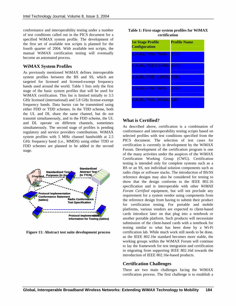
WiMAX System Profiles As previously mentioned WiMAX defines interoperable system profiles between the BS and SS, which are targeted for licensed and licensed-exempt frequency bands used around the world. Table 1 lists only the first stage of the basic system profiles that will be used for WiMAX certification. This list is limited initially to 3.5 GHz licensed (international) and 5.8 GHz license-exempt frequency bands. Data bursts can be transmitted using either FDD or TDD schemes. In the TDD scheme, both the UL and DL share the same channel, but do not transmit simultaneously, and in the FDD scheme, the UL and DL operate on different channels, sometimes simultaneously. The second stage of profiles is pending regulatory and service providers contributions. WiMAX system profiles with 5 MHz channel bandwidth at 2.5 GHz frequency band (i.e., MMDS) using either TDD or FDD schemes are planned to be added in the second stage.
Figure 11: Abstract test suite development process
Table 1: First-stage system profiles for WiMAX certification
1st Stage Profile Configuration
Profile Name
3.5GHz, TDD, 7MHz 3.5T1
3.5GHz, TDD 3.5MHz 3.5T2
3.5GHz, FDD, 3.5MHz 3.5F1
3.5GHz, FDD, 7MHz 3.5F2
5.8GHz, TDD, 10MHz 5.8T
What is Certified? As described above, certification is a combination of conformance and interoperability testing scripts based on selected profiles with test conditions specified from the PICS document. The selection of test cases for certification is currently in development by the WiMAX Forum. Development of the certification program is one of the many activities under the auspices of the WiMAX Certification Working Group (CWG). Certification testing is intended only for complete systems such as a BS or an SS, not individual solution components such as radio chips or software stacks. The introduction of BS/SS reference designs may also be considered for testing to show that the design conforms to the IEEE 802.16 specification and is interoperable with other WiMAX Forum Certified equipment, but will not preclude any requirement for a system vendor using components from the reference design from having to submit their product for certification testing. For portable and mobile platforms, various vendors are expected to client-based cards introduce later on that plug into a notebook or another portable platform. Such products will necessitate submission of the client-based cards with a notebook for testing similar to what has been done by a Wi-Fi certification lab. While much work still needs to be done, as the IEEE 802.16e standard becomes more stable, the working groups within the WiMAX Forum will continue to lay the framework for test integration and certification in migrating from supporting IEEE 802.16d towards the introduction of IEEE 802.16e-based products.
Certification Challenges There are two main challenges facing the WiMAX certification process. The first challenge is to establish a
Protocol Implementation Conformance Statement (tables)
PICS
Standardized Test Purposes (in English) TPs Standard
Standardized Abstract Test Suite (in TTCN) ATS
Protocol Implementation eXtra Information for Testing (tables)
IXIT
RCT
Radio Conformance Test Specification
Profiles Protocol Implementation Conformance Statement (tables)
PICS PICS
Standardized Test Purposes (in English) TPs TPs Standard
Standardized Abstract Test Suite (in TTCN) ATS ATS
Protocol Implementation eXtra Information for Testing (tables)
IXIT IXIT
RCT RCT
Radio Conformance Test Specification
Profiles Profiles

Intel Technology Journal, Volume 8, Issue 3, 2004
Global, Interoperable Broadband Wireless Networks: Extending WiMAX Technology to Mobility 185
WiMAX certification lab with all the necessary resources and equipment. The second challenge is to have all the necessary specialized test equipment such as a Protocol Analyzer (PA) ready for use by the certification lab.
Certification Lab Set-up Establishing a WiMAX certification lab presents several unique and important requirements to be successful. Since this new technology is based on an open standard, the test-bed must be validated before the certification can be started. To accomplish this, the following key issues must be addressed:
• Availability of BS/SS from different vendors with different Si solutions.
• Specialized test equipment to analyze, track, and report test results.
• Integration of testing methodology with the vendor hardware, test equipment, and test scripts called out in the test plan.
• Establishing a baseline of acceptable test results from available hardware in the test bed.
• Ability to replicate the test configuration so vendors can conduct their own pre-testing.
Protocol Analyzer Development The WiMAX Forum is facilitating the development of a PA through a third party to help analyze the transmitted DL and UL IP packets between a BS and SS based on the WiMAX PICS document. Figure 12 shows, for example, a WiMAX test-bed configuration using the PA. In this configuration, the controller turns test scripts into test commands, which are then issued to the traffic simulator, PA, and Device Under Test (DUT). The PA development challenge is the system integration of a modified BS hardware platform with different radios for both licensed and license-exempt frequency bands with a software emulation tool. The key features of the PA system include the following: • Data packet capture and display o Display multiple levels of information (summary,
decode tree, raw data packets, etc.). o Ability to correlate capture data with test results.
• Display of message sequence charts. • Ability to trigger on packet content (protocol, field
values, patterns) and on extended sequences of events.
• Display of statistics of collected data. • Generation of summary and detailed diagnostic test
automated alarm generation capability. • Support of a flexible scripting interface that enables
users to create custom scripts and to control PA
functions in order to aid the diagnosis of failed test cases.
Figure 12: WiMAX protocol analyzer test-bed
configuration
In the second stage of the PA development, it is expected that the PA will be able to emulate either the BS or SS in order to analyze the prohibited test cases.
In conclusion, the building blocks for the WiMAX certification process, which include both conformance and interoperability testing, were reviewed. The key challenges facing the Industry today include setting up the WiMAX certification lab with the PA to validate their test-bed using BS/SS from different equipment vendors. Furthermore, the participation of multiple vendors in public plugfest events is critical to ensure the Industry-wide acceptance of WiMAX certified units.
CONCLUSION Although wireless networks and radio coverage in general have proliferated over the years, data service offerings continue to be either limited in range (as in 802.11) or deficient in data speed and cost as in Wireless Wide Area Networks (WWANs). Wireless data rates for WWANs are limited and are of high-cost partly due to the inherently granular physical and network layer specifications that burden the WWAN RAN and core switching fabric, and partly due to the limited available bandwidth for operation. As extended battery life and reduced size of laptops affords increased portability, so does the need for ubiquitous connectivity with rich data content at affordable prices become more urgent. By delivering a combination of higher modulation schemes within greater channel bandwidths and link budget
BSBSBSSSSSSSSS
SignalAnalysis
Traffic Generator
PA
LAN/GPIB
Wireless ChannelImpairments
SignalAnalysis
PA
UL Trigger
DHCP TFTP TOD
Controller
Test setup
DUT
Intruder
DL Trigger
GPIB
GPIB
BSBSBSSSSSSSSS
SignalAnalysis
Traffic Generator
PA
LAN/GPIB
Wireless ChannelImpairments
SignalAnalysis
PA
UL Trigger
DHCP TFTP TOD
Controller
Test setup
DUT
Intruder
Test setup
DUT
Intruder
DL Trigger
GPIB
GPIB

Intel Technology Journal, Volume 8, Issue 3, 2004
Global, Interoperable Broadband Wireless Networks: Extending WiMAX Technology to Mobility 186
margins that are comparable to wide area wireless systems, IEEE 802.16 is uniquely positioned to extend broadband wireless beyond the small islands of service afforded by Wi-Fi systems today. Incremental evolution, from Fixed access to Portability and then to Full Mobility, with laptops and PDAs enabled with IEEE 802.16, furthers Intel’s vision of coupling wireless connectivity and computing in a single processor platform. The set of ongoing activities outlined in this article, a PHY and MAC layer specification that unites the market behind a common set of standards, a flexible end-to-end network architecture that is coupled with a coherent service vision, and an efficient certification process that enables interoperability, are key enablers for realizing the WiMAX vision.
ACKNOWLEDGMENTS The authors thank Gerald Lebizay, Glenn Begis, Tim Teckman, and David Putzolu for their review of this paper.
REFERENCES [1] “Part 16: Air Interface for Fixed Broadband Wireless
Access Systems,” IEEETM P802.16-REVd/D5-2004.
[2] “Part 16: Air Interface for Fixed and Mobile Broadband Wireless Access Systems,’ IEEETM P802.16e/D3-2004.
[3] “WiMAX PICS for WirelessMAN-OFDM and WirelessHUMAN(-OFDM) Rev.7f (2004).”
[4] “3GPP TS 22.234–Requirements on 3GPP System to WLAN Interworking (Release 6).”
[5] “3GPP TS 23.234–3GPP system to WLAN Interworking; System Description (Release 6).”
[6] RFC 2865, “Remote Authentication Dial In User Service,” Related RFCs at http://www.freeradius.org/rfc/*
[7] RFC 3588, “DIAMETER base protocol.”
[8] RFC 3344, “IP Mobility support for IPv4.”
[9] RFC 3775, “Mobility support in IPv6.”
[10] RFC 2475, “An architecture for differentiated services.”
[11] RFC 3031, “Multiprotocol label switching architecture.”
[12] DNS RFCs can be found at http://www.dns.net/dnsrd/rfc/*
[13] RFC 793, “Transmission Control Protocol.”
AUTHORS’ BIOGRAPHIES Ed Agis is a market development manager for the Wireless Broadband Division (WBD) at Intel Corporation. He is also the co-chair of the WiMAX Forum Certification Working Group and a member of the WiMAX Technical and Marketing Working Groups. Ed holds a B.Sc. degree from the Air Force Academy graduating Magna cum Laude as well as a Masters of Business Administration in Management and another in Operations/Product Marketing from Amber University. His e-mail is ed.agis at intel.com.
Henry Mitchel is a systems architect in Intel’s Modular Communications Platform Division within the Communications Infrastructure Group specializing in chip architectures, firmware, protocols, and standards, and their impacts on systems architecture. Prior to joining Intel he was director of R&D at DataStorm Technologies, Inc., makers of PROCOMM PLUS*. He holds a BS degree from the Massachusetts Institute of Technology and an MS degree from the University of Missouri. His e-mail is henry.mitchel at intel.com.
Shlomo Ovadia received a Ph.D. degree in Optical Sciences from the Optical Sciences Center, University of Arizona in 1984. He held various technical positions at IBM, Bellcore, and General Instruments before joining Intel in 2000 as principal architect in CTG, where he was leading the effort on the architecture, design, and development of optical burst switching in enterprise networks. Currently at ICG, Shlomo is leading Intel’s WiMAX interoperability and certification effort for IEEE 802.16d/e-based wireless products. He is the author of a recently published book titled Broadband Cable TV Access Networks: From Technologies to Applications (Prentice Hall, 2001). He is a senior member of IEEETM/LEOS/COMSOC with more than 70 technical publications and conference presentations. He is the holder of 35 patents, and his personal biography is included in the Millennium edition of Who’s Who in Science and Engineering (2000/2001). His e-mail is shlomo.ovadia at intel.com.
Selim Aissi is lead MID and security architect in the Virtualization and Trust Lab at Intel’s Corporate Technology Group. He also leads standards efforts in 3GPP. Before joining Intel in 1999, he worked at the University of Michigan, General Dynamics’ M1A2 Battlefield Tank Division, General Motors’ Embedded Controller Excellence Center, and Applied Dynamics International. Selim serves on the review board of several
* Other brands and names are the property of their respective owners.
Intel Technology Journal, Volume 8, Issue 3, 2004
Global, Interoperable Broadband Wireless Networks: Extending WiMAX Technology to Mobility 187
publications and conferences, including ACM CCS, ACM SWS, and he is the vice-chair of the Security and Management (SAM) Conference. He holds a Ph.D. degree in Aerospace Engineering from the University of Michigan and is a senior member of the IEEE and ACM. His e-mail is selim.aissi at intel.com.
Sanjay Bakshi is an 802.16e network architect in Intel’s Mobile Networking Lab within the Corporate Technology Group. Prior to joining the Mobile Networking Lab, Sanjay was engineering manager and architect in the Performance Networking Lab within the Corporate Technology Group. He has led a number of projects related to the usage of the Intel Internet Exchange Processor in various fields such as IP routing, MPLS, 3G wireless, and next-generation control plane architecture. Sanjay received his B.E. degree in Computer Science from the Regional Engineering College, Tiruchirapalli, India. His e-mail is sanjay.bakshi at intel.com.
Prakash Iyer is a senior staff architect in Intel’s Mobile Networking Lab within the Corporate Technology Group. He is an active member of the IEEE 802.16 Working Group including chair for the Handoff Adhoc group. He leads standards efforts in the IEEE, IETF, 3GPP, and 3GPP2 on heterogeneous wireless interworking and directs architecture, prototyping, and simulation efforts for seamless networking–including 802.11 and 802.16. He holds B.S. degrees in Physics and Electrical and Computer Engineering and an M.S. degree in Computer Science. His e-mail is prakash.iyer at intel.com.
Masud Kibria is 802.16e initiative manager within Intel’s Communications Technology Lab focused on the technical validation of 802.16e. Prior to joining Intel, Masud led various strategic projects at AT&T Wireless including WCDMA evolution to HSDPA, Interoperability for 2.5G/3G Networks, WLAN, Wireless-PBX, emerging technology feasibility studies, etc. Previously, he has worked on various theoretical and practical aspects of coverage, capacity, and interference for mobile wireless systems and has led regional teams in WWAN design, implementation, and operation. Masud received his BSEE degree from the University of Maryland. His e-mail is masud.kibria at intel.com.
Christopher B. Rogers is a WWAN technology strategist within Intel’s Communications Technology Labs. Prior to his current focus on 802.16 technology, he was marketing director and co-founder of Intel’s Ultrawideband Wireless Group and has also held business development and marketing roles in other WPAN- and WWAN-related businesses within Intel. Chris is a member of IEEE 802.15 and 802.16 and chairs an
industry specifications subgroup for mobile broadband wireless architecture. He received his Bachelors degree in engineering from Georgia Institute of Technology and holds an MBA degree from Carnegie Mellon University. His e-mail is chris.b.rogers at intel.com.
James Tsai is a wireless network and mobile platform architect in Intel’s Mobile Networking Lab within the Corporate Technology Group. His research work has focused on wireless network architectures (Wi-Fi, WiMAX, and WWAN) and next-generation mobile platform technologies such as extended mobile access technology and multi-radio subsystems. He received his B.S degree in Electrical Engineering from the Chinese Culture University in Taiwan and an M.S. degree in Computer Science from Columbia University. His e-mail is james.tsai at intel.com.
Copyright © Intel Corporation 2004. This publication was downloaded from http://developer.intel.com/.
Legal notices at http://www.intel.com/sites/corporate/tradmarx.htm.

Intel Technology Journal, Volume 8, Issue 3, 2004
Global, Interoperable Broadband Wireless Networks: Extending WiMAX Technology to Mobility 188
THIS PAGE INTENTIONALLY LEFT BLANK
RF System and Circuit Challenges for WiMAX 189
RF System and Circuit Challenges for WiMAX
Balvinder Bisla, Intel Communications Group, Intel Corporation Roger Eline, Intel Communications Group, Intel Corporation
Luiz M. Franca-Neto, Intel Communications Group, Intel Corporation
Index words: WiMAX, I/Q, IF, FDD, TDD
ABSTRACT
Broadband Wireless Access has occupied a niche in the market for about a decade, but with the signing of the 802.16d standard it could finally explode into the mass market. Intel’s baseband transceiver chip is flexible enough to accommodate Radio Frequency Integrated Circuit (RFIC) architectures of today and the future. With the emergence of this standard an ecosystem is developing that will allow multiple vendors to produce components that adhere to a standard specification and hence allow large-scale deployment. One of the major challenges of the 802.16d standard is the plethora of options that exist; Worldwide Interoperability Microwave Access (WiMAX) will address this issue by limiting options and hence ensure interoperability. The result will allow manufacturers of Radio Frequency (RF) components and test equipment to have their products used for mass deployment.
In this paper, we focus on the various RF challenges that exist on a RF system-level and show how such challenges can translate into circuit designs. The RF is made more complicated by the fact that WiMAX indeed addresses wireless markets across the world both in licensed and unlicensed bands. Thus, solutions have to be flexible enough to allow for the many RF frequency bands and different regulations around the globe. Several major RF architectures are discussed and the implications for WiMAX specifications are explored, in particular both Intermediate Frequency (IF)- and I/Q-based structures are investigated.
Part of our discussion will provide insight into the cost and performance tradeoffs between Time Division Duplex (TDD) and Frequency Division Duplex (FDD) systems both in licensed and unlicensed bands. It is generally accepted that TDD systems offer cost advantages over their FDD counterparts; however, most licensed bands intended for data applications operate with FDD systems in mind. Some of the RF subsystem
blocks that have stringent WiMAX specifications are also elaborated upon: these include synthesizers, power amplifiers, and filtering. These fundamental subsystem blocks are where most of the transceiver costs reside; the same blocks are also responsible for most of the RF performance.
The industry is moving towards using Orthogonal Frequency Division Multiplexing Access (OFDMA) and either spatial diversity or beam forming techniques to enhance link margins. We touch on the RF challenges associated with these techniques. Finally, we view some of the important WiMAX specifications for RF and the implications for the design of RF circuits, which include SNDR, channel bandwidths, RF bands, noise figures, output power levels, and gain setting. Some important differences between WiMAX and 802.11 RF specifications are also highlighted.
INTRODUCTION As the RF challenges mount so do the costs of the Radio. For WiMAX to be successful the cost vs. performance equation has to be balanced carefully. Two extreme examples of this cost and performance equation are a Single In Single Out (SISO) system from Hybrid Networks (now defunct) requiring Line of Sight (LOS) radios. LOS radios result in truck rollouts utilizing experienced technicians to set the equipment up. However the cost of the radio is low due to its simplicity. In general, the SISO radio requires expensive installation and reliability is poor; link margins are typically 145 dB. On the other hand, Iospan Wireless (now defunct) demonstrated a Multiple In Multiple Out (MIMO) radio with a 3x2 system; i.e., three receive and two transmit chains. It was able to support link margins of 165 dB that could penetrate inside homes in multipath environments. With this ability, the issue of costly truck rollouts is eliminated; however, the cost of the multiple radio chains becomes a deterrent. Still, as Radio Frequency Integrated Circuit (RFIC) integration

Intel Technology Journal, Volume 8, Issue 3, 2004
RF System and Circuit Challenges for WiMAX 190
improves, costs will head down. WiMAX, through the use of integration and advanced techniques to increase link margins, should be able to achieve reliable wireless systems at a reasonable cost.
RF ARCHITECTURES This section describes the plethora of tradeoffs and challenges for RF architectures for WiMAX-related radios. We discuss Frequency Division Duplex (FDD) and its cousin, Half FDD (HFDD) as well as Time Division Duplex (TDD). Intermediate Frequency (IF), Direct Conversion or Zero Intermediate Frequency (ZIF) as well as variants of these are presented. The interface between the Baseband (BB) chip and the radio must be carefully designed, so these challenges are exposed. Methods to improve Link Margins, namely MIMO, and beam forming can be used in WiMAX. In addition, OFDMA, which allows for subchannelization, improves capacity efficiency. We discuss the RF challenges inherent in the use of these methods.
TDD/FDD and HFDD Architectures
TDD Figure 1 shows a TDD radio. The darkened blocks are the most costly in the radio. TDD systems utilize one frequency band for both Transmit and Receive. This concept requires only one Local Oscillator (LO) for the radio. In addition only one RF filter is necessary and this filter is shared between the Transmitter (TX) and the Receiver (RX). The synthesizer and RF filters are major cost drivers in radios. Having one synthesizer saves on die area; a large part of the radio die size can be taken up by the LO, in particular the inductor, which is part of the resonant structure.
The RF filter in a TDD system is not required to attenuate its TX noise as severely as in FDD systems. The TDD mode prevents the TX noise from self jamming the RX since only one is on at any time. As well as relief of the RF filter specifications, having just one RF filter saves cost and space. It should be noted that to ensure Transmitting radios do not interfere with nearby Receiving radios, the specification for TX noise cannot be eased with abandon. The Transmission noise from Radio 1 will interfere with the Received signal of Radio 2. Thus, although self-jamming specifications are made easier, collocation specifications must be carefully considered. There is a notable savings in power from the TDD architecture, a direct result of turning the RX off while in TX mode and vice versa.
Several disadvantages exist, however. There is a reduction of data throughput since there is no transmission of data while in RX mode unlike FDD
systems. The Medium Access Control (MAC)-level software tends to have a more complicated scheduler than an FDD system since it must deal with synchronizing many users’ time slots in both TX and RX mode. It must be noted that while the RF filtering specifications are relaxed, this tends to imply that subscriber stations will have to be spaced further apart from each other to avoid interference. In essence, the system must handle fewer users in a given area than in FDD systems.
TDD systems are most prominent in unlicensed bands; in these bands the regulations for output noise are more relaxed than in licensed bands. Thus, inexpensive RF filters can be specified. Since the unlicensed bands are free of cost there is competition to drive for the lowest cost architecture, TDD.
FDD Figure 2 shows an FDD radio. A high-performance RF front-end is required in FDD systems. Collocation issues from a TX noise perspective are solved since the worst-case scenario of self jamming is not possible. FDD systems do not have to switch the RX or TX; this alleviates settling time specifications, which results in a simpler radio design. The MAC software is simpler because it does not have to deal with the time synchronization issues as in TDD systems.
The radio must be capable of data transmission while in Receive mode without incurring any degradation in Bit Error Rate (BER). To ease the burden on the filter there is a gap between the TX frequency band and the RX band; however, carriers wish to minimize this space. Typically this is a separation of 50 MHz to 100 MHz.

Intel Technology Journal, Volume 8, Issue 3, 2004
RF System and Circuit Challenges for WiMAX 191
Figure 1: TDD radio
Figure 2: FDD radio
Figure 3: HFDD radio
We try to specify the TX noise to be 10 dB below the RX input noise floor, in which case the TX noise will only degrade the RX by 0.5 dB. Unfortunately the specifications usually tie FDD systems to using cavity
filters or 4-pole ceramic filters. Cavity filters run in the order of $35 each while ceramic filters can be in the $8 range. Most licensed bands do not have one standard structure but are flexible; i.e., the TX and RX could be
Intel Technology Journal, Volume 8, Issue 3, 2004
RF System and Circuit Challenges for WiMAX 192
swapped in different geographical regions. This results in having to design several flavors of the filters, something that does not lend itself to mass production of the filters.
To give an idea of the filter requirements in FD:
Filter_rej (dB) = Po(dBm/Hz) – Mask (dBc)-[174+NF-cochannel_rej]
For example, if power output Po = -33 dBm/Hz, in a 1 MHz signal bandwidth, output power is +27 dBm.
Mask of TX is = 60 dBc; i.e., the thermal floor of TX is 60 dB below the Po.
NF is Noise Figure of Receiver = 5 dB.
CoChannel_rej is how far in dB is the undesired signal below the desired signal. = 10 dB i.e., the undesired signal is 10 dB below the desired signal.
We get Filter_rej at the RX frequency of 86 dB. If the RX is 100 MHz away from the TX, this filter is an expensive cavity filter.
The full-duplex nature of the circuit requires a separate TX and RX synthesizer. The RFIC die area is significantly impacted by the inductor of a resonant circuit; this is part of a Voltage Controlled Oscillator (VCO) which is used in the synthesizer. Thus, two of these have a large impact on the cost of the RFIC.
A final note on FDD systems is that they are power hungry; this also increases the cost of the power system. Thus, FDD is not an ideal platform to build portable or mobile radios.
FDD systems are typically deployed in licensed bands e.g., 5.8 GHz, 3.5 GHz, 2.5 GHz: the spectrum is expensive. The cost of the spectrum forces the carriers to serve as many users as possible. Capacity must be optimized, which results in carriers favoring FDD architecture. Clearly it is very desirable to have the Base Station work in FDD, but to reduce costs, the Subscriber Station could be a HFDD structure.
HFDD Figure 3 shows a HFDD radio. The HFDD architecture combines the benefits of the TDD systems while still trying to allow for frequency duplexing. The Base Station can operate in FDD and retain its capacity advantage over TDD systems. This can lower the cost of the radio significantly at the Subscriber Station where the unit cost must be driven down.
The cost reduction appears in the form of relief in the RF TX filter, and since there is one synthesizer the die area of the RFIC shrinks. Power savings are also realized as in TDD systems.
Once again the collocation issues have to be addressed carefully. Self jamming is not a problem as in TDD but then too much relief on the TX filter can result in interference between users.
There is also a capacity loss at the Subscriber Station since the radio cannot simultaneously Transmit and Receive.
The HFDD structure can be used in both licensed and unlicensed bands. The Transmit and Receive can be at the same frequency as in TDD systems or separated by a frequency gap as in FDD. This type of radio is very flexible. Its cost structure approaches that of a TDD radio.
In summarizing the duplexing schemes, Intel’s baseband chip can support both TDD and HFDD modes. This takes care of most of the Subscriber Stations. In a typical deployment the ratio between the Base Station and Subscriber Stations is 1 to 100, due to the low volume of the Base Station. The Physical (PHY) and Media Access Control (MAC) layer need not be designed as a custom chip; a Field Programmable Gate Array (FPGA) could be cost effective. It is possible to connect two baseband chips together to support an FDD scenario for the Base Station.
We discuss various radio architectures in the following sections; these include IF- and I/Q-based architectures and some variants on these. Some of the interface between the radio and the baseband chip is deliberated.
RF Interface The baseband chip digitizes the analog signal and performs signal processing. This PHY layer chip contains the blocks for filtering, Automatic Gain Control (AGC), demodulation of data, security, and framing of data. The algorithms that do power measurements, such as AGC and RF selection can be taken care of by the lower-level MAC. As can be seen, there are common parameters such as AGC that are shared across the PHY, MAC, and radio.
The major blocks within a radio that need control from the baseband IC are AGC, frequency selection, sequencing of the TX/RX chain, monitoring of TX power, and any calibration functions e.g., I/Q imbalance. Each of these blocks are tightly coupled with the PHY and/or lower-level MAC.
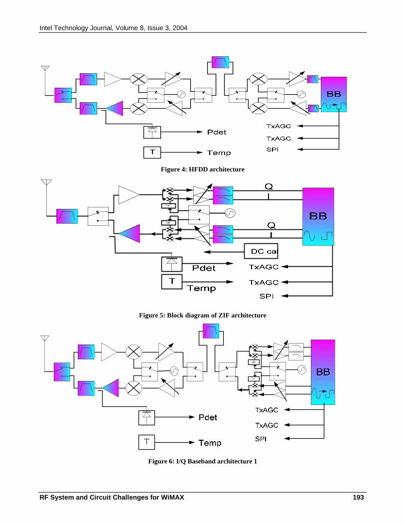
Intel Technology Journal, Volume 8, Issue 3, 2004
RF System and Circuit Challenges for WiMAX 193
Figure 4: HFDD architecture
Figure 5: Block diagram of ZIF architecture
Figure 6: I/Q Baseband architecture 1
Intel Technology Journal, Volume 8, Issue 3, 2004
RF System and Circuit Challenges for WiMAX 194
A reasonable way to communicate with the radio is through a Serial Peripheral Interface (SPI); it minimizes pins on the RFIC.
Usually the SPI is used to control the synthesizer. In order to make the interface more useful so that it can control the digital AGC of an RFIC and help perform measurements of power and temperature, the SPI needs to be a dedicated time-critical element. In this way, the SPI can respond to AGC, measurements, and frequency commands in a timely and predictable manner. A note of caution, however: traffic on the SPI could cause interference to the incoming signal and put spurs on the TX signal. Therefore all SPI communication should only occur in the TX to RX time gaps. Other interface blocks are General Purpose Input/Output (GPIO), Pulse Width Modulators (PWM), DACs, and ADCs.
The AGC is split into RX AGC and TX AGC. In the RX AGC, response times may have to be rapid to cope with the changing RF channel in a mobile environment, in the order of usec. However, in a fixed wireless application, the channel change is in the order of msec. The TX AGC can be relatively slow in steady state. However, in powering up the TX, the AGC may need to attain the correct power level in the usec time frame. Typically, the AGC is controlled through single-bit digital to analog converter, i.e., sigma delta converters. Either of these methods have clock noise that needs to be filtered out. The tradeoff here is that for a large slope of the RF AGC, the clock noise must be filtered to avoid distorting the signal. However, the filtering introduces a delay that slows down the AGC response. To increase the time response of the AGC, multibit DACs can be used.
The selection of the RF is done through the SPI. For HFDD systems there is a settling time from TX to RX frequency, and the loading of the SPI is part of the timing budget.
Monitoring the temperature of the radio is a slow process; however, power measurements either from TX or RX require synchronization with the TX/RX timing gaps. Interfacing to the radio must take into account the sequencing of the radio; for example, in the case of the Transmitter we need to switch the antenna, enable the TX and load frequency, change the TX gain, turn on the PA, and finally ramp the modulation. Switching to the RX requires sequencing the TX down to avoid spurious emissions.
Two fundamental parameters drive radio design: noise and linearity. The goal is to attain as much dynamic range in the presence of undesired signals. This requires a distribution of gain and filtering through the TX or RX chain. Many architecture designers struggle with the
placement of this gain and filtering. We look at some of these radio architectures in the next sections.
HFDD Architecture The details of the HFDD architecture are shown in Figure 4. There is a frequency separation between the TX and RX so separate filtering is necessary in the RF front-end. However, the IF is shared between the TX and RX. A Surface Acoustic Wave (SAW) filter provides for excellent adjacent/alternate channel rejection. There is a final frequency conversion to a lower IF that can be handled by an AD. Much of the AGC range is at the lower IF. An AGC range of 70 dB is required; the absolute gain is higher to overcome losses. For the TX AGC, a 50 dB range is required. The AGC can be controlled through PWMs for analog AGC or GPIO for step attenuators.
Two synthesizers are necessary for the double conversion. The low-frequency synthesizer is fixed and does not have to be switched during the RX to TX change. The high frequency synthesizer is the challenging block; it is required to settle within 100 usec. The step size could be as low as 125 KHz in the 3.5 GHz band.
Several signals are also sent to the Baseband IC: TX power level (sometimes RX power level), temperature, and synthesizer lock detect. The power level is most important since power output has to be as close as possible to the intended value and still within regulations.
TDD Architecture TDD is a good example of direct conversion transceivers or ZIF. Figure 5 is a block diagram of the ZIF architecture. The TX and RX frequencies are the same so the RF filter can be shared. The downconversion process is done with I/Q mixers; these consume a small area on the die. The issue with such mixers is they need to be matched; otherwise, distortion is introduced. Also LO feedthrough effects tend to increase due to dc imbalances. These effects are significant since most of the gain is at the final conversion. The dc offset results in a reduction in the dynamic range of the AD since extra bits are required for this offset. A dc calibration circuit can be implemented to reduce the effect. In addition, I/Q imbalance will result in distortion. The problems are aggravated by temperature, gain changes, and frequency. By going to dc, low-pass filters can be used that are selective to channels. These can be implemented on chip and can save on cost. It must be noted that the on-chip low-pass filters do consume a large die area. They can also introduce noise. WiMAX

Intel Technology Journal, Volume 8, Issue 3, 2004
RF System and Circuit Challenges for WiMAX 195
has variable bandwidths ranging from 1 MHz to 14 MHz but as the cut-off frequency is reduced there are significant challenges in the on-chip filter. For such ZIF schemes there must be an Automatic Frequency Control (AFC) loop whereby the Baseband IC controls the reference oscillator of the RFIC. This ensures that any dc leakage terms stay at dc and do not spill over into the desired tones of the OFDM waveform.
I/Q Baseband Architecture 1 A variant of the HFDD and TDD architectures mentioned above is a combination shown in Figure 6. This structure has the advantage that some filtering is done at an IF removing some of the strain on the dc filters.
In addition, power can be saved by having the final stage operate at lower frequencies. The issues related to I/Q mismatch and dc leakage are lessened by having less gain at dc and operating the mixers at an IF instead of an RF. Savings can be realized at the TX filtering: because the SAW can do most of the filtering there is no need for the TX low-pass filters. This has the added advantage that the I/Q mismatch from the low-pass filters is removed. One drawback is that two Digital to Analog (DA) converters and two Analog to Digital (DA) converters are required.
I/Q Baseband Architecture 2 To address the problems of the I/Q baseband radios another architecture is considered. Figure 7 shows an RX where the signal is mixed to dc then mixed up to a near Zero IF (NZIF). By going to dc the IF filter is removed and filtering can be done on-chip. To avoid dc and I/Q problems the signal is mixed to an IF. The choice of IF is greater than half the channel bandwidth. This structure allows the gain to be distributed between the dc and IF stages. Also, as an added benefit, only one AD is required. For the TX stage, I/Q upconversion is used.
RF Challenges for MIMO, AAS, and OFDMA Antenna diversity is an important technique that can inexpensively enhance the performance of low-cost subscriber stations. It can help mitigate the effects of channel impairments like multipath, shadowing, and interference that severely degrade a system’s performance, and in some cases make it inoperable. By using multiple antennas, a system’s link budget can be significantly improved by reducing channel fading, and in some implementations, by providing array gain. There are several designs, all of which yield excellent gains, that can be implemented, ranging from low to high complexity. The basic designs are Selection
Diversity Combining (SDC), Equal Gain Combining (EGC), and Maximum Ratio Combining (MRC). SDC is a scheme of sampling the receive performance of multiple antenna branches and selecting the branch that maximizes the receiver signal to noise ratio. To work properly each antenna branch must have relatively independent channel fading characteristics. To achieve this, the antennas are either spatially separated, use different polarization, or are a combination of both. The spatial correlation of antennas can be approximated by the zero order Bessel function given by the equation ρ=J0
2(2пd/λ) and shown in Figure 8. From Figure 8, it is seen that relatively uncorrelated antenna branches can be achieved for spatial separations greater than one-third a wavelength, supporting the requirement for small form-factor subscriber stations.
For optimal SDC performance the selection process and data gathering must be completed within the coherence time. The coherence time is the period over which a propagating wave preserves a near-constant phase relationship both temporally and spatially. After the coherence time has elapsed the antennas should be re-sampled to account for expected channel variations and to allow for re-selection of the optimal antenna. For a TDD system, where reciprocal uplink (UL) and downlink (DL) channel characteristics are expected, the selected receive antenna can also be used as the transmit antenna. Although the SDC technique sounds rather simple, surprisingly large system gain improvements are possible if the algorithms can be designed effectively.
There are two figures of merit for judging the gain enhancement of an antenna diversity scheme. These are diversity gain and array gain. Under changing channel conditions, diversity gain is equivalent to the decrease in gain variance of local signal strength fluctuations of a multiantenna array system when compared to a single-antenna array system. The result of increased diversity gain is the reduction in fading depth. This is due to each antenna of a multiantenna system experiencing independent fading channels over frequency and time. The second figure of merit, array gain, is the accumulation of antenna gain associated with increased directivity via a multiantenna array system. In a typical system, as the number of antenna array elements grows, the gain increases 10*log (n), where n is the number of antenna array elements. This means a doubling of gain for every doubling of antenna elements.

Intel Technology Journal, Volume 8, Issue 3, 2004
RF System and Circuit Challenges for WiMAX 196
Figure 7: I/Q Baseband architecture 2
Figure 8: Bessel function approximation of the spatial correlation coefficient
The SDC scheme exhibits no array gain, as only one from n antennas is used at any instance. However, through spatial or polarization diversity, the SDC achieves stellar diversity gain, as shown in Table 1.
Table 1: Performance enhancement of antenna diversity
Antenna Diversity Scheme
(4 Antenna Branches)
Antenna Gain
(SUI3,SUI4 model w/100uSec Rayleigh delay spread)
Implemen- tation
Complexity
Selection Diversity Combining
8 dB Low
Equal Gain Combining
(Analog)
9 dB Mid
Maximum Ratio Combining (Analog)
10 dB High
Maximum Ratio Combining (Digital)
14 dB High
Another basic antenna diversity technique using multiple antennas is EGC. Instead of selecting one from n antennas, as in SDC, the algorithm combines the power of all antennas. The multiple independent signal branches are co-phased, the gain of each branch set to unity (equal gain), and then all branches combined. The EGC antenna diversity technique achieves diversity gain, while also producing array gain. Thus, EGC provides higher antenna diversity gain then SDC, as can be seen in Table 1. To achieve an antenna diversity benefit closer to optimal, MRC of the antenna elements
Spatial Correlation vs Antenna Spacing
00.10.20.30.40.50.60.70.80.9
1
0 0.2 0.4 0.6 0.8 1
Antenna Spacing (normalized to wavelength)
Co
rrel
atio
n C
oef
fici
ent

Intel Technology Journal, Volume 8, Issue 3, 2004
RF System and Circuit Challenges for WiMAX 197
can be used. This technique is similar to EGC, with the exception that the algorithm tries to optimally adjust both the phase and gain of each element prior to combining the power of all antennas. The summation of the signals may be done in either the analog or digital domain. When summation occurs in the digital domain, RF hardware for each independent antenna branch is required from RF to baseband. When MRC is realized in the analog domain, summation may occur directly at RF. Performance is better when processing is done in the digital domain, as frequency selective channel characteristics are compensated for in each branch. In an analog MRC, only the average channel distortion over frequency is used to compensate for the amplitude and phase variation between array elements. In digital MRC, discrete frequency components across the signal bandwidth are co-phased and individually weighted based on SNR at the receiver. MRC realizes the highest antenna diversity gain compared to the other techniques discussed, (refer to Table 1). Although the complexity is high, MRC implementation costs are decreasing through better RF integration and reduced CMOS geometries of the baseband processor integrated circuit.
MIMO and AAS systems are used to improve link margins. Using MIMO requires multiple RF chains with multiple ADs. With integration, the cost of these multiple chains should come down. Isolation between the receive chains needs to be in the order of 20 dB, which is easy to accomplish. There are no matching requirements for the gain and phase between the RX chains, which means that the radio design is simplified. MIMO works well in TDD or FDD, and its improvements to link margins are observed in multipath environments.
In contrast, for AAS or beam forming systems, the TX and RX chain need to be matched across frequency and over gain and phase. However the subscriber station does not have multiple chains. Such systems work well in TDD mode since the TX frequency is the same as RX frequency. AAS estimate the TX channel based on information they get from the RX channel, so having the same frequency improves these estimates.
OFDMA allows the RF channel to be split into subchannels. As a result, the power can be boosted since fewer tones are used. For users that do not TX much data on the UL, a smaller bandwidth can be allocated. Thus, more efficient use of the bandwidth can be made on a per-user basis. This technique does pose some challenges for the radio. Interference and noise between subchannels must be carefully considered over the whole transmit gain range. This problem is similar to the FDD case except there is no frequency separation. Therefore, noise performance and linearity must be
excellent since there is no help from filtering. Another issue with OFDMA is that the RF must be maintained to <1% accuracy; otherwise, different users will collide with each other within the subchannels.
We have discussed various duplex schemes: RF architectures were outlined and some methods to improve link margin considered. Next, we discuss the particular circuit blocks within the RF system that are particular cost drivers.
RF SYSTEM BLOCKS There are three main areas of cost for a radio: synthesizer, power amplifier, and filter.
Synthesizer The synthesizer generates the LO that mixes with the incoming RF to create a lower frequency signal that can be digitized and processed by the Baseband IC. The WiMAX specifications call for a high-performance synthesizer. The synthesizer block takes up a large part of the RFIC die area and is therefore a costly component of the RFIC. The Integrated Phase Noise is <1deg rms with an integration frequency of 1/20 of the tone spacing to ½ the channel bandwidth. Thus, for the smaller bandwidths of 1.75 MHz, the integration of the phase noise can start as low as 100 Hz. For HFDD architectures, the TX to RX frequency has to settle within 100 usecs. The step size of the channel is 125 KHz in the 3.5 GHz band. In order to settle and maintain this step size, fractional synthesizers must be considered. It must be noted that as RF increases, obtaining phase noise <1deg rms becomes a challenge. As well as all the radio LOs, the clock for the AD must be also viewed as an LO that adds phase noise to the overall jitter specification.
Power Amplifier Wideband digital modulation requires a high degree of linearity. Linearity implies higher power consumption. The tradeoff between efficiency and linearity is a constant battle. For WiMAX, a power amplifier can work at 4 to 5% efficiency for about a 6 dB backoff from output P1 dB. Such a backoff results in about a 2.5% Error Vector Magnitude (EVM) or 32 dBc of Signal to Noise plus Distortion (SNDR). With a class AB Power Amplifier (PA) the efficiencies can run as high as 15 to 18% with similar EVM numbers.
A much overlooked parameter in PA design is settling time. When a PA is switched on from cold the power level will overshoot (or undershoot), then settle out. This settling time can be as poor as 100s of msec to get within 0.1 dB of the final value. For OFDM symbols,

Intel Technology Journal, Volume 8, Issue 3, 2004
RF System and Circuit Challenges for WiMAX 198
the RX has to estimate the power of a tone from the beginning of a frame to the end of a frame. If there is a droop of power from the beginning to the end of >0.1 dB across the frame, the BER for 64 Quadrature Amplitude Modulation (QAM) will increase. The primary cause for this power droop is that the bias circuits and the output power Field Effect Transistor (FET) are at thermally different points. Since this phenomenon is thermal the effect can last 100s of msec. To mitigate power droop the bias circuits have to be placed as close to the output FETs as possible so they see the same temperature. In some cases the PA may have to be turned on ahead of the TX cycle to allow the PA to stabilize and remove some of the droop. This implies having a trigger signal based on when data are to be transmitted. Having the MAC and PHY realize this trigger is not a simple matter. The budget of 100 usec for HFDD is taken up by the synthesizer settling and any PA turn-on issues. A possible solution is to design the PA so that the PA settling is <5 usec.
Filtering Filtering is required to eliminate undesired signals from adjacent or alternate channels. Any noise from these immediate signals can leak noise into the desired band. Filtering at the receiver does not help; only a clean transmitted signal will prevent such degradation. Regulatory bodies control the transmitted mask.
For the adjacent channel problem the challenge is between linearity and filtering complexity. If the undesired channels are filtered out then less backoff in the radio is required and more of the AD bits are available for fading margin. SAW filters have depreciated in cost and are now in the <$2 range for high volume. SAWs provide the optimum filtering. A significant drawback is that the technology does fix the maximum channel bandwidth that can be supported. Another issue is that it is difficult to support a large array of RF bands with a fixed IF. For spurious analysis, the optimum IF depends on the RF.
Filtering on-chip requires a large die area and as the channel bandwidth is reduced the die size increases. On-chip filters also produce more noise. A benefit is that the filter can be adjusted to accommodate the various bandwidths.
For I/Q-based designs, on-chip filters are necessary. The filters can be matched much more closely if on-chip. This minimizes the I/Q mismatch due to filtering. The final channel selectivity is performed in the Baseband IC using digital filters.
Filtering, like gain, must be distributed between the RF and subsequent down conversions. The RF filtering is
used to reduce the image and far blockers; i.e., out of the RF band. The RF front-end must be linear enough to support the largest in-band blocker. In addition, reciprocal mixing of the LO with the undesired signal must be considered. The RF filters are typically >50 MHz wide and are constructed from various technologies each with different Qs. The larger the Q, the larger the size and the better filter shape. In FDD systems cavity filters may have to be used; these are large mechanical cavities and can cost >$30 in high volume.
WIMAX SPECIFICATIONS We highlight some of the WiMAX RF specifications and contrast them with 802.11 specifications where possible. The specifications are broken into RX and TX. It should be noted that most designs aim to do better than the standards, hence these numbers should be viewed as the minimum requirements. In addition we note the impact on the RFIC due to these specifications.
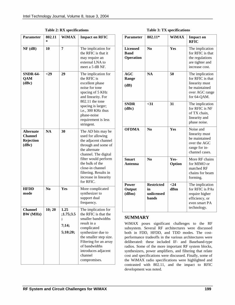
Intel Technology Journal, Volume 8, Issue 3, 2004
RF System and Circuit Challenges for WiMAX 199
Table 2: RX specifications
Parameter 802.11*
WiMAX Impact on RFIC
NF (dB) 10 7 The implication for the RFIC is that it may require an external LNA to meet a 5 dB NF.
SNDR-64-QAM (dBc)
<29 29 The implication for the RFIC is excellent phase noise for tone spacing of 5 KHz and linearity. For 802.11 the tone spacing is larger; i.e., 300 KHz thus phase-noise requirement is less stringent.
Alternate Channel Rejection (dBc)
NA 30 The AD bits may be used for allowing the adjacent channel through and some of the alternate channel. The digital filter would perform the bulk of the close-in channel filtering. Results in increase in linearity for RFIC.
HFDD mode
No Yes More complicated synthesizer to support dual frequency.
Channel BW (MHz)
10; 20 1.25 ;1.75;3.5;
7;14;
5;10;20;
The implication for the RFIC is that the smaller bandwidths result in a complicated synthesizer due to the smaller step size. Filtering for an array of bandwidths introduces adjacent channel compromises.
Table 3: TX specifications
Parameter 802.11* WiMAX Impact on RFIC
Licensed Band Operation
No Yes The implication for RFIC is that the regulations are tighter and increase cost.
AGC Range
(dB)
NA 50 The implication for RFIC is that linearity must be maintained over AGC range for 64-QAM.
SNDR (dBc)
<31 31 The implication for RFIC is NF of TX chain, linearity and phase noise.
OFDMA No Yes Noise and linearity must be maintained over the AGC range for in-channel cases.
Smart Antenna
No Yes-Option
More RF chains for MIMO or matched RF chains for beam forming.
Power Output (dBm)
Restricted in unlicensed bands
<24 dBm
The implication for RFIC is PAs require higher efficiency, or even smart PA technology.
SUMMARY WiMAX poses significant challenges to the RF subsystem. Several RF architectures were discussed both in FDD, HFDD, and TDD modes. The cost-performance tradeoffs in the various architectures were deliberated: these included IF- and Baseband-type radios. Some of the more important RF system blocks, synthesizers, power amplifiers, and filtering that relate cost and specifications were discussed. Finally, some of the WiMAX radio specifications were highlighted and contrasted with 802.11, and the impact to RFIC development was noted.

Intel Technology Journal, Volume 8, Issue 3, 2004
RF System and Circuit Challenges for WiMAX 200
REFERENCES [1] 802.16 REV d/D5- 2004.
[2] P.Vizmuller, RF Circuits and Systems, Artech House, MA, USA, 1995.
AUTHORS’ BIOGRAPHIES Balvinder Bisla received his B.Sc. degree at Sussex University, England in 1984. He then worked at Rutherford Appleton Labs in the UK before moving to the USA to work on wireless metering and global positioning systems. He was a principal RF engineer with Iospan Wireless where they developed the world’s first MIMO-OFDM system. Currently, he is working at Intel on RF and microwave communication issues for WiMAX products. His e-mail is Balvinder.s.Bisla at intel.com.
Roger Eline received a B.S.E.E. degree from UC Davis and an M.S.E.E from Santa Clara University in 1991. Since then his work has focused on RF and microwave communication system development. He currently works for the Broadband Wireless Division of Intel, where he manages the Platform Engineering Group. He has been with Intel for one and a half years developing low-cost IEEE 802.16 baseband and radio reference platforms based on Intel’s IEEE 802.16 baseband processor/modem ASIC. His e-mail is Roger.j.eline at intel.com.
Luiz M. Franca-Neto earned his Electronic Engineering degree, with distinction, from ITA/CTA, SJC, Sao Paulo, Brazil, in 1989, and he received the TASA award for being first in class in communications. He received his M.Sc. and Ph.D. degrees from Stanford University, all in Electrical Engineering, in 1995 and 1999, respectively. From 1990 to 1992, he was a design engineer with ALCATEL/Elebra Telecom for public telecommunications and optical line terminal equipment. In USA from 1993-1996, he has worked for HP-Labs, Palo Alto, CA, and Texas Instruments, Dallas, TX. He was with Intel R&D Labs from 1999-2004, where he led research on CMOS for RF/Microwave/Millimeter wave frequencies. He created new circuit design methods such as “backing off” for LNAs and “optimum pump” for VCOs with demonstrated circuits operating from 2.4 GHz to 100 GHz (a world record for CMOS). He led the investigations for substrate noise in Pentium® 4 processors and deep nwell isolation where he articulated ® Pentium is a registered trademark of Intel Corporation or its subsidiaries in the United States and other countries.
how substrate noise spectrum structure can be exploited for full integration of digital processors and RF delicate circuits in the same die. Also in the labs, Luiz led the research to move all RF passives from the die to the substrate package in order to realize higher performance RF System-on-Package and free silicon area for hosting more digital functions and general-purpose processors. Since February 2004, Luiz leads the WiMAX RF & Analog IC internal development within the ICG/BWD group in Santa Clara. His homepage is http://www-snow.stanford.edu/~franca*.
Copyright © Intel Corporation 2004. This publication was downloaded from http://developer.intel.com/.
Legal notices at http://www.intel.com/sites/corporate/tradmarx.htm.

Intel Technology Journal, Volume 8, Issue 3, 2004
Scalable OFDMA Physical Layer in IEEE 802.16 WirelessMAN 201
Scalable OFDMA Physical Layer in IEEE 802.16 WirelessMAN
Hassan Yaghoobi, Intel Communications Group, Intel Corporation
Index words: OFDMA, Scalable, IEEE 802.16, WirelessMAN, subchannel, subcarrier ABSTRACT
The concept of scalability was introduced to the IEEE 802.16 WirelessMAN Orthogonal Frequency Division Multiplexing Access (OFDMA) mode by the 802.16 Task Group e (TGe). A scalable physical layer enables standard-based solutions to deliver optimum performance in channel bandwidths ranging from 1.25 MHz to 20 MHz with fixed subcarrier spacing for both fixed and portable/mobile usage models, while keeping the product cost low. The architecture is based on a scalable subchannelization structure with variable Fast Fourier Transform (FFT) sizes according to the channel bandwidth. In addition to variable FFT sizes, the specification supports other features such as Advanced Modulation and Coding (AMC) subchannels, Hybrid Automatic Repeat Request (H-ARQ), high-efficiency uplink subchannel structures, Multiple-Input-Multiple-Output (MIMO) diversity, and coverage enhancing safety channels, as well as other OFDMA default features such as different subcarrier allocations and diversity schemes. The purpose of this paper is to provide a brief tutorial on the IEEE 802.16 WirelessMAN OFDMA with an emphasis on scalable OFDMA.
INTRODUCTION The IEEE 802.16 WirelessMAN standard [1] provides specifications for an air interface for fixed, portable, and mobile broadband wireless access systems. The standard includes requirements for high data rate Line of Sight (LOS) operation in the 10-66 GHz range for fixed wireless networks as well as requirements for Non Line of Sight (NLOS) fixed, portable, and mobile systems operating in sub 11 GHz licensed and licensed-exempt bands.
Because of its superior performance in multipath fading wireless channels, Orthogonal Frequency Division Multiplexing (OFDM) signaling is recommended in OFDM and WirelessMAN OFDMA Physical (PHY) layer modes of the 802.16 standard for operation in sub 11
GHz NLOS applications. OFDM technology has been recommended in other wireless standards such as Digital Video Broadcasting (DVB) [2] and Wireless Local Area Networking (WLAN) [3]-[4], and it has been successfully implemented in the compliant solutions.
Amendments for PHY and Medium Access Control (MAC) layers for mobile operation are being developed (working drafts [5] are being debated at the time of publication of this paper) by TGe of the 802.16 Working Group. The task group’s responsibility is to develop enhancement specifications to the standard to support Subscriber Stations (SS) moving at vehicular speeds and thereby specify a system for combined fixed and mobile broadband wireless access. Functions to support optional PHY layer structures, mobile-specific MAC enhancements, higher-layer handoff between Base Stations (BS) or sectors, and security features are among those specified. Operation in mobile mode is limited to licensed bands suitable for mobility between 2 and 6 GHz.
Unlike many other OFDM-based systems such as WLAN, the 802.16 standard supports variable bandwidth sizes between 1.25 and 20 MHz for NLOS operations. This feature, along with the requirement for support of combined fixed and mobile usage models, makes the need for a scalable design of OFDM signaling inevitable. More specifically, neither one of the two OFDM-based modes of the 802.16 standard, WirelessMAN OFDM and OFDMA (without scalability option), can deliver the kind of performance required for operation in vehicular mobility multipath fading environments for all bandwidths in the specified range, without scalability enhancements that guarantee fixed subcarrier spacing for OFDM signals.
The concept of scalable OFDMA is introduced to the IEEE 802.16 WirelessMAN OFDMA mode by the 802.16 TGe and has been the subject of many contributions to the standards committee [6]-[9]. Other features such as AMC subchannels, Hybrid Automatic Repeat Request
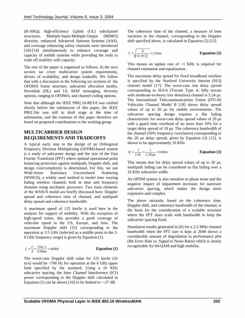
Intel Technology Journal, Volume 8, Issue 3, 2004
Scalable OFDMA Physical Layer in IEEE 802.16 WirelessMAN 202
(H-ARQ), high-efficiency Uplink (UL) subchannel structures, Multiple-Input-Multiple-Output (MIMO) diversity, enhanced Advanced Antenna Systems (AAS), and coverage enhancing safety channels were introduced [10]-[14] simultaneously to enhance coverage and capacity of mobile systems while providing the tools to trade off mobility with capacity.
The rest of the paper is organized as follows. In the next section we cover multicarrier system requirements, drivers of scalability, and design tradeoffs. We follow that with a discussion in the following six sections of the OFDMA frame structure, subcarrier allocation modes, Downlink (DL) and UL MAP messaging, diversity options, ranging in OFDMA, and channel coding options.
Note that although the IEEE P802.16-REVd was ratified shortly before the submission of this paper, the IEEE P802.16e was still in draft stage at the time of submission, and the contents of this paper therefore are based on proposed contributions to the working group.
MULTICARRIER DESIGN REQUIREMENTS AND TRADEOFFS A typical early step in the design of an Orthogonal Frequency Division Multiplexing (OFDM)-based system is a study of subcarrier design and the size of the Fast Fourier Transform (FFT) where optimal operational point balancing protection against multipath, Doppler shift, and design cost/complexity is determined. For this, we use Wide-Sense Stationary Uncorrelated Scattering (WSSUS), a widely used method to model time varying fading wireless channels both in time and frequency domains using stochastic processes. Two main elements of the WSSUS model are briefly discussed here: Doppler spread and coherence time of channel; and multipath delay spread and coherence bandwidth.
A maximum speed of 125 km/hr is used here in the analysis for support of mobility. With the exception of high-speed trains, this provides a good coverage of vehicular speed in the US, Europe, and Asia. The maximum Doppler shift [15] corresponding to the operation at 3.5 GHz (selected as a middle point in the 2-6 GHz frequency range) is given by Equation (1).
Hzm
smf
m408
086.0
/35 ===λν Equation (1)
The worst-case Doppler shift value for 125 km/hr (35 m/s) would be ~700 Hz for operation at the 6 GHz upper limit specified by the standard. Using a 10 KHz subcarrier spacing, the Inter Channel Interference (ICI) power corresponding to the Doppler shift calculated in Equation (1) can be shown [16] to be limited to ~-27 dB.
The coherence time of the channel, a measure of time variation in the channel, corresponding to the Doppler shift specified above, is calculated in Equation (2) [15].
msf
Tm
C03.1
16
92
=⋅⋅
=π
Equation (2)
This means an update rate of ~1 KHz is required for channel estimation and equalization.
The maximum delay spread for fixed broadband wireless is specified by the Stanford University Interim (SUI) channel model [17]. The worst-case rms delay spread corresponding to SUI-6 (Terrain Type A: hilly terrain with moderate-to-heavy tree densities) channel is 5.24 µs. The International Telecommunications Union (ITU-R) Vehicular Channel Model B [18] shows delay spread values of up to 20 µs for mobile environments. The subcarrier spacing design requires a flat fading characteristic for worst-case delay spread values of 20 µs with a guard time overhead of no more than 10% for a target delay spread of 10 µs. The coherence bandwidth of the channel (50% frequency correlation) corresponding to the 20 µs delay spread, given by Equation (3) [15], is shown to be approximately 10 KHz.
KHzs
BC
10205
1
5
1=
⋅=
⋅≈
µστ
Equation (3)
This means that for delay spread values of up to 20 µs, multipath fading can be considered as flat fading over a 10 KHz subcarrier width.
An OFDM system is also sensitive to phase noise and the negative impact of impairment increases for narrower subcarrier spacing, which makes the design more expensive and complex.
The above rationale, based on the coherence time, Doppler shift, and coherence bandwidth of the channel, is the basis for the consideration of a scalable structure where the FFT sizes scale with bandwidth to keep the subcarrier spacing fixed.
Simulation results generated in [6] for a 2.5 MHz channel bandwidth when the FFT size is kept at 2048 shows a considerable amount of degradation in performance plot (Bit Error Rate vs. Signal to Noise Ratio) which is clearly recognizable for 64-QAM and high mobility.
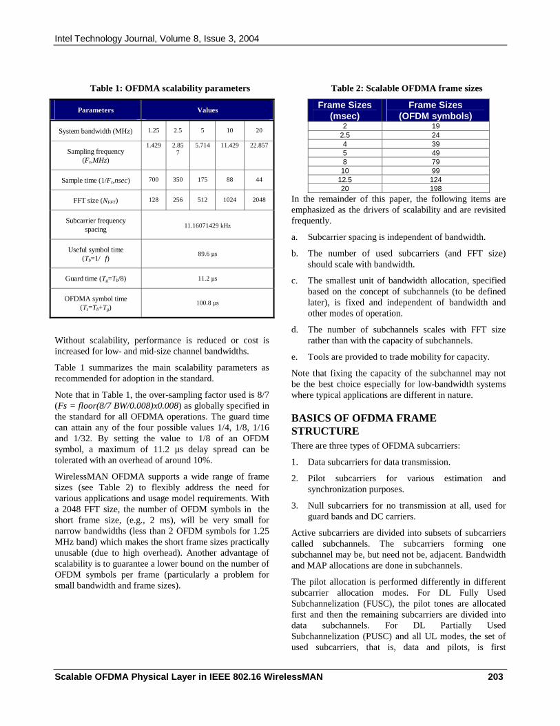
Intel Technology Journal, Volume 8, Issue 3, 2004
Scalable OFDMA Physical Layer in IEEE 802.16 WirelessMAN 203
Table 1: OFDMA scalability parameters
Parameters Values
System bandwidth (MHz) 1.25 2.5 5 10 20
Sampling frequency (Fs,MHz)
1.429 2.857
5.714 11.429 22.857
Sample time (1/Fs,nsec) 700 350 175 88 44
FFT size (NFFT) 128 256 512 1024 2048
Subcarrier frequency spacing 11.16071429 kHz
Useful symbol time (Tb=1/ f)
89.6 µs
Guard time (Tg=Tb/8) 11.2 µs
OFDMA symbol time (Ts=Tb+Tg)
100.8 µs
Without scalability, performance is reduced or cost is increased for low- and mid-size channel bandwidths.
Table 1 summarizes the main scalability parameters as recommended for adoption in the standard.
Note that in Table 1, the over-sampling factor used is 8/7 (Fs = floor(8/7 BW/0.008)x0.008) as globally specified in the standard for all OFDMA operations. The guard time can attain any of the four possible values 1/4, 1/8, 1/16 and 1/32. By setting the value to 1/8 of an OFDM symbol, a maximum of 11.2 µs delay spread can be tolerated with an overhead of around 10%.
WirelessMAN OFDMA supports a wide range of frame sizes (see Table 2) to flexibly address the need for various applications and usage model requirements. With a 2048 FFT size, the number of OFDM symbols in the short frame size, (e.g., 2 ms), will be very small for narrow bandwidths (less than 2 OFDM symbols for 1.25 MHz band) which makes the short frame sizes practically unusable (due to high overhead). Another advantage of scalability is to guarantee a lower bound on the number of OFDM symbols per frame (particularly a problem for small bandwidth and frame sizes).
Table 2: Scalable OFDMA frame sizes
Frame Sizes (msec)
Frame Sizes (OFDM symbols)
2 19 2.5 24 4 39 5 49 8 79 10 99
12.5 124 20 198
In the remainder of this paper, the following items are emphasized as the drivers of scalability and are revisited frequently.
a. Subcarrier spacing is independent of bandwidth.
b. The number of used subcarriers (and FFT size) should scale with bandwidth.
c. The smallest unit of bandwidth allocation, specified based on the concept of subchannels (to be defined later), is fixed and independent of bandwidth and other modes of operation.
d. The number of subchannels scales with FFT size rather than with the capacity of subchannels.
e. Tools are provided to trade mobility for capacity.
Note that fixing the capacity of the subchannel may not be the best choice especially for low-bandwidth systems where typical applications are different in nature.
BASICS OF OFDMA FRAME STRUCTURE There are three types of OFDMA subcarriers:
1. Data subcarriers for data transmission.
2. Pilot subcarriers for various estimation and synchronization purposes.
3. Null subcarriers for no transmission at all, used for guard bands and DC carriers.
Active subcarriers are divided into subsets of subcarriers called subchannels. The subcarriers forming one subchannel may be, but need not be, adjacent. Bandwidth and MAP allocations are done in subchannels.
The pilot allocation is performed differently in different subcarrier allocation modes. For DL Fully Used Subchannelization (FUSC), the pilot tones are allocated first and then the remaining subcarriers are divided into data subchannels. For DL Partially Used Subchannelization (PUSC) and all UL modes, the set of used subcarriers, that is, data and pilots, is first
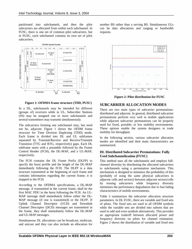
Intel Technology Journal, Volume 8, Issue 3, 2004
Scalable OFDMA Physical Layer in IEEE 802.16 WirelessMAN 204
partitioned into subchannels, and then the pilot subcarriers are allocated from within each subchannel. In FUSC, there is one set of common pilot subcarriers, but in PUSC, each subchannel contains its own set of pilot subcarriers.
Figure 1: OFDMA frame structure (TDD, PUSC)
In a DL, subchannels may be intended for different (groups of) receivers while in UL, Subscriber Stations (SS) may be assigned one or more subchannels and several transmitters may transmit simultaneously.
The subcarriers forming one subchannel may, but need not be, adjacent. Figure 1 shows the OFDM frame structure for Time Division Duplexing (TDD) mode. Each frame is divided into DL and UL subframes separated by Transmit/Receive and Receive/Transmit Transition (TTG and RTG, respectively) gaps. Each DL subframe starts with a preamble followed by the Frame Control Header (FCH), the DL-MAP, and a UL-MAP, respectively.
The FCH contains the DL Frame Prefix (DLFP) to specify the burst profile and the length of the DL-MAP immediately following the FCH. The DLFP is a data structure transmitted at the beginning of each frame and contains information regarding the current frame; it is mapped to the FCH.
According to the OFDMA specifications, a DL-MAP message, if transmitted in the current frame, shall be the first MAC PDU in the burst following the FCH. An UL-MAP message shall immediately follow either the DL-MAP message (if one is transmitted) or the DLFP. If Uplink Channel Descriptor (UCD) and Downlink Channel Descriptor (DCD) messages are transmitted in the frame, they shall immediately follow the DL-MAP and UL-MAP messages.
Simultaneous DL allocations can be broadcast, multicast, and unicast and they can also include an allocation for
another BS rather than a serving BS. Simultaneous ULs can be data allocations and ranging or bandwidth requests.
Figure 2: Pilot distribution for FUSC
SUBCARRIER ALLOCATION MODES There are two main types of subcarrier permutations: distributed and adjacent. In general, distributed subcarrier permutations perform very well in mobile applications while adjacent subcarrier permutations can be properly used for fixed, portable, or low mobility environments. These options enable the system designers to trade mobility for throughput.
In the following section, various subcarrier allocation modes are identified and their main characteristics are summarized.
DL Distributed Subcarrier Permutations: Fully Used Subchannelization (FUSC) This method uses all the subchannels and employs full-channel diversity by distributing the allocated subcarriers to subchannels using a permutation mechanism. This mechanism is designed to minimize the probability of hits (probably of using the same physical subcarriers in adjacent cells and sectors) between adjacent sectors/cells by reusing subcarriers while frequency diversity minimizes the performance degradation due to fast fading characteristics of mobile environments.
Table 3 summarizes the subcarrier allocation structure parameters. In DL FUSC, there are variable and fixed sets of pilots. The fixed sets are used in all OFDM symbols while the variable sets are divided into subsets that are used in odd and even symbols alternatively. This provides an appropriate tradeoff between allocated power and frequency diversity on pilots for channel estimation. Figure 2 shows the distribution of variable and fixed sets
Pre
ambl
eD
L-M
AP
FCH
UL-
MA
P
UL-
MA
P
DL Burst SS1DL Burst
SS3
DL BurstBroadcast
DL Burst SS2
DL BurstSS1
(from BS2)
DL BurstSS4
DL BurstMulticast
S+1
S+2
S
S+L
UL Burst SS1
UL Burst SS2
UL Burst SS3
UL Burst SS4
RNG/BW-REQ
OFDMA Symbol Number
Su
b-ch
anne
l Lo
gica
l Num
ber
Pre
ambl
eD
L-M
AP
UL-
MA
P
k k+1 k+3 k+5
DL Sub-frame UL Sub-frameTTG RTG
k+7 k+9 k+11 k+13 k+15 k+18 k+21 k+23 k+24
0 200 400 600 800 1000 1200 1400 1600 1800Sub-carrier Physical Index
Pilo
t Set
s
Variable Set #1Variable Set #2Fixed Set #1Fixed Set #2

Intel Technology Journal, Volume 8, Issue 3, 2004
Scalable OFDMA Physical Layer in IEEE 802.16 WirelessMAN 205
of pilots in the case of 2048 FFT. Pilot sets for other FFT sizes are subsets of those for the 2048 FFT.
Table 3: DL distributed subcarrier permutation (FUSC)
Parameters Values
System bandwidth (MHz) 1.25 2.5 5 10 20
FFT size (NFFT) 128 N/A** 512 1024 2048
Number of guard subcarriers
22 N/A 86 173 345
Number of used subcarriers 106 N/A 426 851 1703
Number of data subcarriers 96 N/A 384 768 1536
Number of pilot subcarriers (uses both variable and
constant sets)
9*
N/A 42 83 166
Number of subchannels 2 N/A 8 16 32
Subcarrier Permutation Uses Permutation Type 1 for Tone Distribution (Eq. 107 [20])
* variable set only
** FFT size of 256 is not supported
Figure 3: DL PUSC cluster structure
DL and UL Distributed Subcarrier Permutation: Partially Used Subchannelization (PUSC) According to the OFDMA specification, all OFDMA DL and UL subframes shall start in DL and UL PUSC mode, respectively. In DL PUSC, subchannels are divided and assigned to three segments that can be allocated to sectors of the same cell. The method employs full-channel diversity by distributing the allocated subcarriers to subchannels. A permutation mechanism is designed to minimize the probability of hits between adjacent sectors/cells by reusing subcarriers, while frequency diversity minimizes the performance degradation due to fast fading characteristics of mobile environments.
Table 4 summarizes the parameters of DL PUSC subcarrier allocation. DL PUSC uses a cluster structure, as illustrated in Figure 3, which spans over two OFDM symbols (in time) of fourteen subcarriers, each with a total of four pilot subcarriers per cluster.
Table 5 summarizes the parameters of UL PUSC subcarrier allocation. UL PUSC uses a tile structure, as
illustrated in Figure 4, that spans over three OFDM symbols (in time) of four subcarriers, each with total of four pilot subcarriers.
Note that because of the DL and UL, cluster and tile structures are composed of two and three OFDM symbols, respectively; the DL and UL subframe size and the granularity of the DL and UL allocations are also two or three OFDM symbols, respectively.
Table 4: DL distributed subcarrier permutation (PUSC)
Parameters Values
System bandwidth (MHz) 1.25 2.5 5 10 20
FFT size (NFFT) 128 N/A 512 1024 2048
Number of guard subcarriers
43 N/A 91 183 367
Number of clusters/subchannels
6/3 N/A 30/15 60/30 120/60
Number of used subcarriers
85 N/A 421 841 1681
Number of data subcarriers
72 N/A 360 720 1440
Number of pilot subcarriers
12 N/A 60 120 240
Subcarrier permutation Uses Permutation Type 1 for Tone Distribution (Eq. 107 [20])
Cluster renumbering Activated
Optional DL Distributed Subcarrier Permutation: Fully Used Subchannelization (OFUSC) This method employs full-channel diversity by distributing the allocated subcarriers to subchannels using a permutation mechanism designed to minimize the probability of hits between adjacent sectors/cells by reusing subcarriers, while frequency diversity minimizes the performance degradation due to fast fading characteristics of mobile environments.
Table 6 summarizes the parameters of OFUSC subcarrier allocation. In OFUSC, pilots are mapped as specified below, which is different from the assignment in the FUSC mode.
Compared to FUSC mode, the number of used subcarriers in this method is considerably larger (1681 vs. 1729). As a result, compliance with spectral mask requirements, without a change in the over-sampling factor, may be a challenge for this mode.
Odd Symbols
Even Symbols
Pilot sub-carriers Pilot sub-carriers
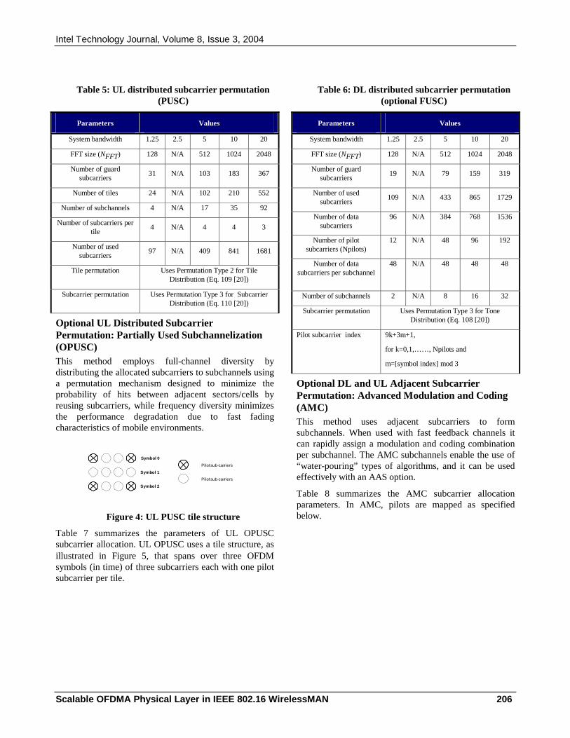
Intel Technology Journal, Volume 8, Issue 3, 2004
Scalable OFDMA Physical Layer in IEEE 802.16 WirelessMAN 206
Table 5: UL distributed subcarrier permutation (PUSC)
Parameters Values
System bandwidth 1.25 2.5 5 10 20
FFT size (NFFT) 128 N/A 512 1024 2048
Number of guard subcarriers
31 N/A 103 183 367
Number of tiles 24 N/A 102 210 552
Number of subchannels 4 N/A 17 35 92
Number of subcarriers per tile
4 N/A 4 4 3
Number of used subcarriers
97 N/A 409 841 1681
Tile permutation Uses Permutation Type 2 for Tile Distribution (Eq. 109 [20])
Subcarrier permutation Uses Permutation Type 3 for Subcarrier Distribution (Eq. 110 [20])
Optional UL Distributed Subcarrier Permutation: Partially Used Subchannelization (OPUSC) This method employs full-channel diversity by distributing the allocated subcarriers to subchannels using a permutation mechanism designed to minimize the probability of hits between adjacent sectors/cells by reusing subcarriers, while frequency diversity minimizes the performance degradation due to fast fading characteristics of mobile environments.
Figure 4: UL PUSC tile structure
Table 7 summarizes the parameters of UL OPUSC subcarrier allocation. UL OPUSC uses a tile structure, as illustrated in Figure 5, that spans over three OFDM symbols (in time) of three subcarriers each with one pilot subcarrier per tile.
Table 6: DL distributed subcarrier permutation (optional FUSC)
Parameters Values
System bandwidth 1.25 2.5 5 10 20
FFT size (NFFT) 128 N/A 512 1024 2048
Number of guard subcarriers
19 N/A 79 159 319
Number of used subcarriers
109 N/A 433 865 1729
Number of data subcarriers
96 N/A 384 768 1536
Number of pilot subcarriers (Npilots)
12 N/A 48 96 192
Number of data subcarriers per subchannel
48 N/A 48 48 48
Number of subchannels 2 N/A 8 16 32
Subcarrier permutation Uses Permutation Type 3 for Tone Distribution (Eq. 108 [20])
Pilot subcarrier index 9k+3m+1,
for k=0,1,……, Npilots and
m=[symbol index] mod 3
Optional DL and UL Adjacent Subcarrier Permutation: Advanced Modulation and Coding (AMC) This method uses adjacent subcarriers to form subchannels. When used with fast feedback channels it can rapidly assign a modulation and coding combination per subchannel. The AMC subchannels enable the use of “water-pouring” types of algorithms, and it can be used effectively with an AAS option.
Table 8 summarizes the AMC subcarrier allocation parameters. In AMC, pilots are mapped as specified below.
Symbol 0
Symbol 2
Pilot sub-carriers
Pilot sub-carriers
Symbol 1

Intel Technology Journal, Volume 8, Issue 3, 2004
Scalable OFDMA Physical Layer in IEEE 802.16 WirelessMAN 207
Table 7: Optional UL distributed subcarrier permutation (OPUSC)
Parameters Values
System bandwidth 1.25 2.5 5 10 20
FFT size (NFFT) 128 N/A 512 1024 2048
Number of guard subcarriers
19 N/A 79 159 319
Number of used subcarriers
109 N/A 433 865 1729
Number of tiles 36 N/A 144 288 576
Number of tiles per subchannel
6 N/A 6 6 6
Number of data subcarriers per subchannel
48 N/A 48 48 48
Number of subchannels 6 N/A 24 48 96
Subcarrier permutation Uses Permutation Type 4 for Tone Distribution (Eq. 111 [20])
Figure 5: UL OPUSC tile structure
Table 8: UL/DL adjacent subcarrier permutation (optional AMC)
Parameters Values
System bandwidth 1.25 2.5 5 10 20
FFT size (NFFT) 128 N/A 512 1024 2048
Number of guard sub-carriers
19 N/A 79 159 319
Number of used sub-carriers (Nused)
109 N/A 433 865 1729
Number of pilots (Npilots) 12 N/A 48 96 192
Number of data sub-carriers
96 N/A 384 768 1536
Number of bands 3 N/A 12 24 48
Number of bins per band 4 N/A 4 4 4
Number of subcarriers per bin (8 data +1 pilot)
9 N/A 9 9 9
Number of subchannels 2 N/A 8 16 32
Sub-carrier permutation None
Pilot subcarrier index 9k+3m+1,
for k=0,1,……, Npilots and
m=[symbol index] mod 3
Figure 6: Multiple zones in Uplink and Downlink subframes
Zone Switching OFDMA PHY also supports multiple subcarrier allocation zones within the same frame to enable the possibility of support for and coexistence of different types of SS’s.
Figure 6 illustrates zone switching within the DL and UL subframes. The switching is performed using an information element included in DL-MAP and UL-MAP.
DL and UL subframes both start in PUSC mode where groups of subchannels are assigned to different segments by the use of dedicated FCH messages. The PUSC subcarrier allocation zone can be switched to a different type of subcarrier allocation zone through a directive from the PUSC DL-MAP. Figure 6 shows the zone switching from the perspective of a PUSC segment. In the figure, the PUSC FCH/DL-MAP for a segment with IDCell X is followed with another possibly data PUSC

Intel Technology Journal, Volume 8, Issue 3, 2004
Scalable OFDMA Physical Layer in IEEE 802.16 WirelessMAN 208
zone for IDCell X. A PUSC zone for another sector/cell with IDCell Y (Y in general is different from X) is allocated next. An FUSC zone for IDCell Z is shown next in the figure. Note that IDCell Z may be the same as IDCell X which means that a PUSC to FUSC switching is scheduled within the segment for Frequency Reuse One operations. A switching to IDCell 0 can be planned for all network broadcast operations.
Optional PUSC, FUSC, and AMC zones in DL subframes and optional PUSC and AMC zones in UL subframes can be similarly scheduled. Allocation of AMC zones enables the simultaneous support of fixed, portable, and nomadic mobility users along with high mobility users (supported in PUSC/FUSC zones).
DIVERSITY OPTIONS OFDMA PHY supports AAS and also a set of second-, third-, and fourth-order transmit diversity options.
With the AAS option, the system uses a multiple-antenna transmission to improve the coverage and capacity of the system while minimizing the probability of outage through transmit diversity, beam forming, and null steering.
Transmit diversity options consist of a comprehensive set of methods based on second- or fourth-order diversity in DL and second-order diversity in UL that can be flexibly chosen to tradeoff capacity and coverage. The set includes both closed- and open-loop options and also supports Spatial Multiplexing (SM) for maximum spectral efficiency.
Advanced Antenna Systems Two optional AAS modes are supported in OFDMA PHY: Diversity-Map Scan and Direct Signaling Method. Diversity-Map Scan supports both diversity (FUSC and PUSC) and adjacent (AMC) subcarrier permutation options. The Direct Signaling Method supports adjacent subcarrier permutation with less overhead in control signaling.
We now discuss the Diversity-Map Scan option when applied to the AMC subcarrier allocation method.
Figure 7 shows the AAS Diversity Map Zone within a frame. The DL subframe includes a non-AAS section and an AAS section specified by information elements provided in the DL MAP.
Within the AAS zone, subchannel numbers 4 and N-4 (N is the index for the last logical subchannel) are allocated to the AAS DL MAP where a pointer to a beamformed broadcast DL MAP is specified. The broadcaset DL MAP provides beamformed private DL and UL MAPs for AAS
users. The figure illustrates a four-antenna configuration where the AAS preamble and AAS DL MAPs structure are repeated multiples of four times to support the corresponding four groups of users.
Figure 7: AAS diversity MAP zone
Within the AAS zone, the AAS BS specifies allocations to be used for SS Ranging. In TDD mode, the BS can extract the channel information required for beam forming from the Ranging Request messages received from the SS’s. In FDD mode, beam forming is done through the AAS Feedback Request and Response messages where channel response information along with mean Received Signal Strength Indicator (RSSI) and Carrier to Interference plus Noise Ratio (CINR) are reported back to the BS by the SS.
Transmit Diversity OFDMA mode supports second-, third- and fourth-order transmit diversity options in DL and second-order transmit diversity in UL. All diversity options are applicable to both diversity and adjacent subcarrier permutations.
Space Time Coding (STC) based on Alamouti algorithm [19] and Frequency Hopping Diversity Code (FHDC) are two options for second-order diversity in DL. Although not specified by the standard, the number of receive antennas can be specified depending on the performance required.
Second-Order STC Second-order STC in DL supports coding rates of 1 and 2 using the following two transmission format matrices.

Intel Technology Journal, Volume 8, Issue 3, 2004
Scalable OFDMA Physical Layer in IEEE 802.16 WirelessMAN 209
−=
+
+
*
1
*
1
ii
ii
SS
SSA Equation (4)
=
+1i
i
S
SB Equation (5)
Here k
S ’s are OFDM symbols in the frequency domain
right before IFFT operation.
The optional STC transmit diversity is also supported in UL using the transmission format matrix A of Equation (4). Matrix B of Equation (5) can be used by two SS’s in a collaborative special multiplexing mode.
Fourth-Order STC The fourth-order transmit diversity in DL supports rates 1, 2, or 4 using the following transmission format matrices A, B, and C, respectively.
−
−
=
++
++
+
+
*
23
*
32
*
1
*
1
00
00
00
00
ii
ii
ii
ii
SS
SS
SS
SS
A Equation (6)
−−−−
=
++++
++++
+++
+++
*
57
*
23
*
46
*
32
*
75
*
1
*
64
*
1
iiii
iiii
iiii
iiii
SSSS
SSSS
SSSS
SSSS
B Equation (7)
=
4
3
2
1
S
S
SS
C Equation (8)
Here, k
S ’s are OFDM symbols in the frequency domain
right before the IFFT operation.
Third-Order STC The third-order transmit diversity in DL supports rates 1, 2, or 3 using the following transmission format matrices A, B, and C, respectively.
−−
=*
34
*
43
*
12
*
21
~~00
~~~~00
~~
SS
SSSS
SS
A Equation (9)
−−=
4387
*
56
*
12
*
65
*
21
~~~~
~~~~
~~~~
SSSS
SSSS
SSSS
B Equation (10)
=
3
2
1
S
S
S
C Equation (11)
In Equations (9) and (10), we have
QI
QI
QI
QI
QI
QI
QI
QI
SSS
SSS
SSS
SSS
SSS
SSS
SSS
SSS
688
577
866
755
244
133
422
311
~
~
~
~
~
~
~
~
+=+=+=+=+=+=+=+=
Equation (12)
where 2/)2(tan 1−=θ , kQkIk
SjSS ⋅+= , θj
kkeXS ⋅= for
8,,2,1 L=k and sXk' are OFDM symbols in the frequency
domain right before the IFFT operation.
Precoding A general KxL precoding matrix W is specified to be applied to the output X of any second-, third- or fourth-order diversity option mentioned earlier. This way an L th order output vector Z of the STC block is transformed into a final K th order vector for transmission on antennas.
XWZ ⋅= Equation (13)
Precoding can be performed either in closed-loop or open-loop form. In the case of open-loop, the BS weights the transmission according to the channel measurement performed on the UL signal, where a reciprocity assumption can be made for a TDD mode, for example. In the case of closed-loop, BS uses the Channel Quality Indications feedback from the SS.
RANGING IN OFDMA The OFDMA PHY specifies a ranging allocation that can be used for ranging as well as bandwidth request. Initial and periodic ranging processes are supported to synchronize the SS’s with the BS at the initial network entry and also periodically during the normal operation. Bandwidth request mechanism is supported so that SS’s can request UL allocations for transmission of data to the BS. A set of 256 special pseudo-noise 144 bit-long ranging codes are divided into three groups for Initial Ranging, Periodic Ranging, and Bandwidth Requests, such that the BS can determine the purpose of the received code by the subset to which the code belongs. One or more groups of six adjacent subchannels are allocated to ranging where the ranging codes are BPSK modulated to the allocation. The SS randomly selects one
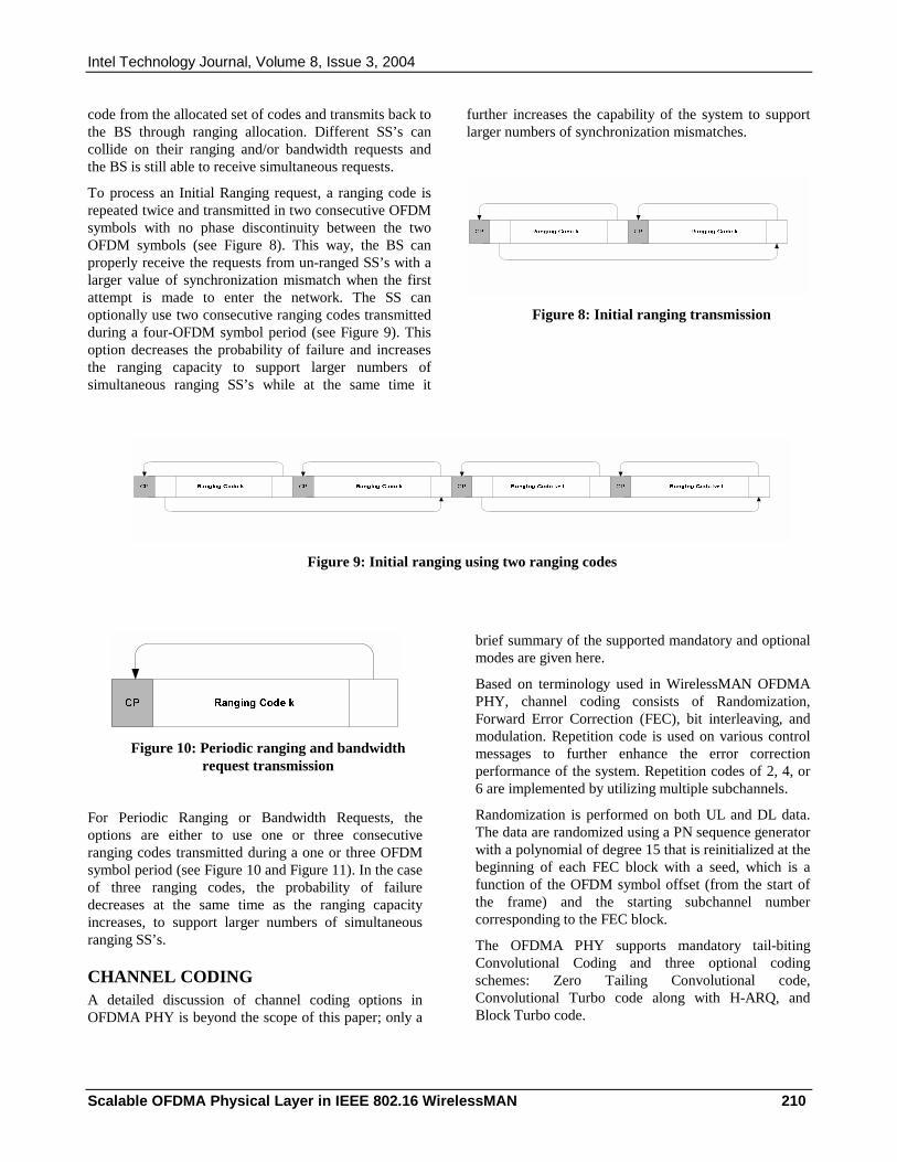
Intel Technology Journal, Volume 8, Issue 3, 2004
Scalable OFDMA Physical Layer in IEEE 802.16 WirelessMAN 210
code from the allocated set of codes and transmits back to the BS through ranging allocation. Different SS’s can collide on their ranging and/or bandwidth requests and the BS is still able to receive simultaneous requests.
To process an Initial Ranging request, a ranging code is repeated twice and transmitted in two consecutive OFDM symbols with no phase discontinuity between the two OFDM symbols (see Figure 8). This way, the BS can properly receive the requests from un-ranged SS’s with a larger value of synchronization mismatch when the first attempt is made to enter the network. The SS can optionally use two consecutive ranging codes transmitted during a four-OFDM symbol period (see Figure 9). This option decreases the probability of failure and increases the ranging capacity to support larger numbers of simultaneous ranging SS’s while at the same time it
further increases the capability of the system to support larger numbers of synchronization mismatches.
Figure 8: Initial ranging transmission
Figure 9: Initial ranging using two ranging codes
Figure 10: Periodic ranging and bandwidth request transmission
For Periodic Ranging or Bandwidth Requests, the options are either to use one or three consecutive ranging codes transmitted during a one or three OFDM symbol period (see Figure 10 and Figure 11). In the case of three ranging codes, the probability of failure decreases at the same time as the ranging capacity increases, to support larger numbers of simultaneous ranging SS’s.
CHANNEL CODING A detailed discussion of channel coding options in OFDMA PHY is beyond the scope of this paper; only a
brief summary of the supported mandatory and optional modes are given here.
Based on terminology used in WirelessMAN OFDMA PHY, channel coding consists of Randomization, Forward Error Correction (FEC), bit interleaving, and modulation. Repetition code is used on various control messages to further enhance the error correction performance of the system. Repetition codes of 2, 4, or 6 are implemented by utilizing multiple subchannels.
Randomization is performed on both UL and DL data. The data are randomized using a PN sequence generator with a polynomial of degree 15 that is reinitialized at the beginning of each FEC block with a seed, which is a function of the OFDM symbol offset (from the start of the frame) and the starting subchannel number corresponding to the FEC block.
The OFDMA PHY supports mandatory tail-biting Convolutional Coding and three optional coding schemes: Zero Tailing Convolutional code, Convolutional Turbo code along with H-ARQ, and Block Turbo code.
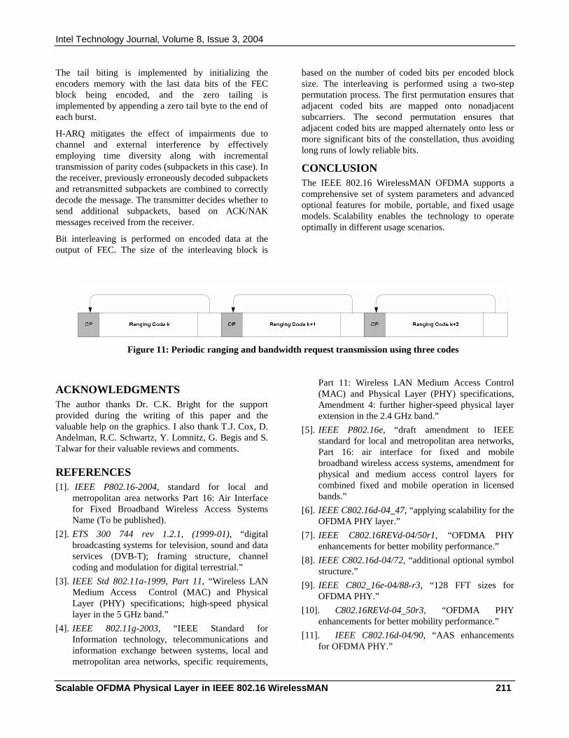
Intel Technology Journal, Volume 8, Issue 3, 2004
Scalable OFDMA Physical Layer in IEEE 802.16 WirelessMAN 211
The tail biting is implemented by initializing the encoders memory with the last data bits of the FEC block being encoded, and the zero tailing is implemented by appending a zero tail byte to the end of each burst.
H-ARQ mitigates the effect of impairments due to channel and external interference by effectively employing time diversity along with incremental transmission of parity codes (subpackets in this case). In the receiver, previously erroneously decoded subpackets and retransmitted subpackets are combined to correctly decode the message. The transmitter decides whether to send additional subpackets, based on ACK/NAK messages received from the receiver.
Bit interleaving is performed on encoded data at the output of FEC. The size of the interleaving block is
based on the number of coded bits per encoded block size. The interleaving is performed using a two-step permutation process. The first permutation ensures that adjacent coded bits are mapped onto nonadjacent subcarriers. The second permutation ensures that adjacent coded bits are mapped alternately onto less or more significant bits of the constellation, thus avoiding long runs of lowly reliable bits.
CONCLUSION The IEEE 802.16 WirelessMAN OFDMA supports a comprehensive set of system parameters and advanced optional features for mobile, portable, and fixed usage models. Scalability enables the technology to operate optimally in different usage scenarios.
Figure 11: Periodic ranging and bandwidth request transmission using three codes
ACKNOWLEDGMENTS The author thanks Dr. C.K. Bright for the support provided during the writing of this paper and the valuable help on the graphics. I also thank T.J. Cox, D. Andelman, R.C. Schwartz, Y. Lomnitz, G. Begis and S. Talwar for their valuable reviews and comments.
REFERENCES [1]. IEEE P802.16-2004, standard for local and
metropolitan area networks Part 16: Air Interface for Fixed Broadband Wireless Access Systems Name (To be published).
[2]. ETS 300 744 rev 1.2.1, (1999-01), “digital broadcasting systems for television, sound and data services (DVB-T); framing structure, channel coding and modulation for digital terrestrial.”
[3]. IEEE Std 802.11a-1999, Part 11, “Wireless LAN Medium Access Control (MAC) and Physical Layer (PHY) specifications; high-speed physical layer in the 5 GHz band.”
[4]. IEEE 802.11g-2003, “IEEE Standard for Information technology, telecommunications and information exchange between systems, local and metropolitan area networks, specific requirements,
Part 11: Wireless LAN Medium Access Control (MAC) and Physical Layer (PHY) specifications, Amendment 4: further higher-speed physical layer extension in the 2.4 GHz band.”
[5]. IEEE P802.16e, “draft amendment to IEEE standard for local and metropolitan area networks, Part 16: air interface for fixed and mobile broadband wireless access systems, amendment for physical and medium access control layers for combined fixed and mobile operation in licensed bands.”
[6]. IEEE C802.16d-04_47, “applying scalability for the OFDMA PHY layer.”
[7]. IEEE C802.16REVd-04/50r1, “OFDMA PHY enhancements for better mobility performance.”
[8]. IEEE C802.16d-04/72, “additional optional symbol structure.”
[9]. IEEE C802_16e-04/88-r3, “128 FFT sizes for OFDMA PHY.”
[10]. C802.16REVd-04_50r3, “OFDMA PHY enhancements for better mobility performance.”
[11]. IEEE C802.16d-04/90, “AAS enhancements for OFDMA PHY.”
Intel Technology Journal, Volume 8, Issue 3, 2004
Scalable OFDMA Physical Layer in IEEE 802.16 WirelessMAN 212
[12]. IEEE 802.16d-04/65, “Enhancing MIMO features for OFDMA PHY layer.”
[13]. IEEE C802.16e-04_72r2, “STC Enhancements for optional FUSC and AMC zones for OFDMA PHY layer.”
[14]. IEEE C802.16e-04/208r2, “space-time codes for 3 transmit antennas for the OFDMA PHY.”
[15]. Rappaport, T.S., Wireless Communications Principles and Practice, Second Edition 2002, Prentice Hall PTR, Upper Saddle River, NJ.
[16]. Li, Y., Cimini, L.J., “Bounds on the Interchannel Interference of OFDM in Time-Varying Impairments,” IEEE Transactions ON Communications, Vol. 49, No. 3, March 2001, pp. 401-404.
[17]. IEEE 802.16.3c-01/29r4, “channel models for fixed wireless applications.”
[18]. Recommendation ITU-R M.1225, “Guidelines for evaluation of Radio transmission technologies for IMT-2000, 1997.”
[19]. Alamouti, S. A., “Simple Transmit Diversity Technique for Wireless Communications,” IEEE Journal on Select Areas in Communications, Vol. 16, No. 8, October 1998.
[20]. IEEE P802.16REVd/D5-2004, standard for local and metropolitan area networks Part 16: Air Interface for Fixed Broadband Wireless Access Systems Name.
AUTHOR’S BIOGRAPHY Hassan Yaghoobi received a B.S. degree from Sharif University of Technology, Tehran, Iran, in 1989 and M.S. and Ph.D. degrees from the University of Maryland, in 1993 and 2000, respectively, all in Electrical Engineering. His academic research interests include nonlinear control theory, communications theory, and digital signal processing.
Hassan’s industrial experience includes communications systems engineering, silicon design/functional definition, and standards development in the area of broadband communications. Since 2000, he has been working at Intel Corporation. As an engineer for Intel’s Broadband Product Group, he worked on silicon functional definition, algorithm design, system design verification, and validation of various cable modem products. He represented Intel at the DOCSIS2.0 Radio Frequency Interface Specification (RFI) and Acceptance Test Plan (ATP) standard committees at Cablelabs. Hassan is currently working as a Strategic Technologist for Intel’s Broadband Wireless Division working on product definitions of Intel’s 802.16d/e silicon
solutions. He is a member of the IEEE 802.16 and 802.20 working groups. He also serves as secretary of the sub 11 GHz Technical Working Group for the WiMAX forum, an industry group focused on interoperability of systems that conform to the IEEE 802.16 standard. Prior to Intel, he worked on design and modeling of wireless terrestrial and satellite receivers for Stanford Telecom and on RF network design of mobile wireless systems for LCC international. His e-mail is hassan.yaghoobi at intel.com.
Copyright © Intel Corporation 2004. This publication was downloaded from http://developer.intel.com/.
Legal notices at http://www.intel.com/sites/corporate/tradmarx.htm.
IEEE 802.16 Medium Access Control and Service Provisioning 213
IEEE 802.16 Medium Access Control and Service Provisioning
Govindan Nair, Intel Communications Group, Intel Corporation Joey Chou, Intel Communications Group, Intel Corporation
Tomasz Madejski, Intel Communications Group, Intel Corporation Krzysztof Perycz, Intel Communications Group, Intel Corporation
David Putzolu, Intel Communications Group, Intel Corporation Jerry Sydir, Intel Communications Group, Intel Corporation
Index words: 802.16 MAC, OFDM, OFDMA, QoS, Service Provisioning, IXA, IA, MIB, WiMAX
ABSTRACT
In this paper we describe the IEEE 802.16 Orthogonal Frequency Division Multiplexing (OFDM) and the 802.16 Orthogonal Frequency Division Multiple Access (OFDMA), Medium Access Control (MAC) protocols, both of which are key elements of the Worldwide Interoperability for Microwave Access Forum (WiMAX) deployments. We also discuss the types of provisioning and Quality of Service (QoS) that can be achieved using the features of this MAC protocol to facilitate the WiMAX deployments. Finally, we review the challenges inherent in implementing this MAC protocol on architectures such as the Intel® IXP network processors and embedded Intel architecture processors to support the application of MAC functionality to the wide range of potential QoS and provisioning approaches.
INTRODUCTION The success of cellular networks in the last decade and the integration of narrowband data solutions into these networks are the first indications that wireless solutions may be able to solve the last mile, a.k.a. the consumer broadband problem. The emergence of Wi-Fi networks has demonstrated that high-bandwidth radio networks are feasible and desirable for both fixed and mobile clients. Finally, recent advances in Radio Frequency (RF) technology, coding algorithms, Medium Access Control (MAC) protocols, and packet processing horsepower have made it possible to achieve the high bandwidths of
® Intel is a registered trademark of Intel Corporation or its subsidiaries in the United States and other countries.
Wi-Fi networks over the extended coverage areas of cellular networks. This fusion, which is realized in the IEEE 802.16 architecture, not only addresses the traditional last mile problem, but also supports nomadic and mobile clients on the go. The architecture enables a “hotzone” deployment model, where high-speed Internet access is provided over large portions of urban areas and along major freeways. In this model, laptops and PDAs operate as Subscriber Stations (SS’s) allowing users to connect to the network in parks, buildings, or wherever they may be.
The broadband wireless architecture is being standardized by the IEEE 802.16 Working Group (WG) and the Worldwide Interoperability for Microwave Access (WiMAX) forum. The 802.16 WG is developing standards for the Physical (PHY) and MAC layers, as well as for the security and higher-layer network model. In this paper we concentrate on the MAC layer and the Quality of Service (QoS) support that is provided by the IEEE 802.16 standard. Throughout the paper, we use the terms 802.16 and WiMAX interchangeably.
In the MAC section we describe the major functions of the 802.16 MAC operating on the Orthogonal Frequency Division Multiplexing (OFDM) and Orthogonal Frequency Division Multiple Access (OFDMA) PHY layers [8]. We then explore the differences in QoS mechanisms in the 802.11 and 802.16 with a view towards pointing out the challenges associated with large-scale WiMAX deployment. We also describe service provisioning and the WiMAX management model that supports self-install and auto-configuration. Finally, in the Implementation Challenges section, we describe two

Intel Technology Journal, Volume 8, Issue 3, 2004
IEEE 802.16 Medium Access Control and Service Provisioning 214
alternate implementations of the 802.16 MAC on an Intel IXP network processor and on an Intel IA processor.
THE MEDIUM ACCESS CONTROL (MAC) LAYER The IEEE 802.16 MAC [8] layer performs the standard Medium Access Control (MAC) layer function of providing a medium-independent interface to the 802.16 Physical (PHY) layer. Because the 802.16 PHY is a wireless PHY layer, the main focus of the MAC layer is to manage the resources of the airlink in an efficient manner. The 802.16 MAC protocol is designed to support Point to Multipoint (PMP) and Mesh network models. In this paper we focus on the PMP network model. The 802.16 MAC protocol is connection oriented. Upon entering the network, each Subscriber Station (SS) creates one or more connections over which their data are transmitted to and from the Base Station (BS). The MAC layer schedules the usage of the airlink resources and provides Quality of Service (QoS) differentiation. It performs link adaptation and Automatic Repeat Request (ARQ) functions to maintain target Bit Error Rates (BER) while maximizing the data throughput. The MAC layer also handles network entry for SS’s that enter and leave the network, and it performs standard Protocol Data Unit (PDU) creation tasks. Finally, the MAC layer provides a convergence sub layer that supports Asynchronous Transfer Mode (ATM) cell- and packet-based network layers.
In the remainder of this section we provide an overview of the functions of the MAC layer. We start with a brief description of the Orthogonal Frequency Division Multiplexing (OFDM) and Orthogonal Frequency Division Multiple Access (OFDMA) PHY layers, and show how they motivate some of the functions that must be performed by the MAC layer for these specific PHYs. We then describe the major functions of the 802.16 MAC protocol.
The OFDM Physical Layer The WirelessMAN-OFDM PHY layer is based on OFDM modulation. It is intended mainly for fixed access deployments, where SS’s are residential gateways deployed within homes and businesses in much the same way as DSL and cable modems are deployed to provide broadband over wireline networks. The OFDM PHY layer supports subchannelization in the Uplink (UL). There are 16 subchannels in the UL. The OFDM PHY layer supports Time Division Duplexing (TDD) and Frequency Division Duplexing (FDD) operations, with support for both FDD and Half-Duplex FDD (H-FDD) SS’s. The specification defines as mandatory, a combined variable-rate Read-Solomon (RS)/Convolutional Coding
(CC) scheme, supporting code rates of 1/2, 2/3, 3/4, and 5/6. Variable-rate Block Turbo Code (BTC) and Convolutional Turbo Code (CTC) are also optionally supported. The standard supports multiple modulation levels, including Binary Phase Shift Keying (BPSK), Quadrature Phase Shift Keying (QPSK), 16-Quadrature Amplitude Modulation (QAM) and 64-QAM. Finally, the PHY supports (as options) transmit diversity in the Downlink (DL) using Space Time Coding (STC) and Adaptive Antenna Systems (AAS) with Spatial Division Multiple Access (SDMA).
The transmit diversity scheme uses two antennas at the BS to transmit an STC encoded signal, in order to provide the gains that result from second-order diversity. Each of two antennas transmits a different symbol (two different symbols) in the first symbol time. The two antennas then transmit the complex conjugate of the same two symbols in the second symbol time. The resulting data rate is the same as without transmit diversity. AAS is used in the 802.16 specification to describe beam forming techniques, where an array of antennas is used at the BS to increase gain to the intended SS, while nulling out interference to and from other SS’s and interference sources. AAS techniques can be used to enable SDMA, where multiple SS’s that are separated in space can receive and transmit on the same subchannel at the same time. By using beam forming, the BS is able to direct the desired signal to the different SS’s and can distinguish between the signals of different SS’s even though they are operating on the same subchannel(s).
Figure 1: Frame structure
Figure 1 illustrates the frame structure for a TDD system. The frame is divided into DL and UL subframes. The DL subframe is made up of a preamble, Frame Control Header (FCH), and a number of data bursts. The FCH specifies the burst profile and the length of one or more DL bursts that immediately follow the FCH. The DL-MAP, UL-MAP, DL Channel Descriptor (DCD), UL
Intel Technology Journal, Volume 8, Issue 3, 2004
IEEE 802.16 Medium Access Control and Service Provisioning 215
Channel Descriptor (UCD), and other broadcast messages that describe the content of the frame are sent at the beginning of these first bursts. The remainder of the DL subframe is made up of data bursts to individual SS’s. Each data burst consists of an integer number of OFDM symbols and is assigned a burst profile that specifies the code algorithm, code rate, and modulation level that are used for those data transmitted within the burst. The UL subframe contains a contention interval for initial ranging and bandwidth allocation purposes and UL PHY PDUs from different SS’s. The DL-MAP and UL-MAP completely describe the contents of the DL and UL subframes. They specify the SS’s that are receiving and/or transmitting in each burst, the subchannels on which each SS is transmitting (in the UL), and the coding and modulation used in each burst and in each subchannel.
If transmit diversity is used, a portion of the DL frame (called a zone) can be designated to be a transmit diversity zone. All data bursts within the transmit diversity zone are transmitted using STC coding. Finally, if AAS is used, a portion of the DL subframe can be designated as the AAS zone. Within this part of the subframe, AAS is used to communicate to AAS-capable SS’s. AAS is also supported in the UL.
In FDD systems, the DL and UL frame structure is similar, except that the UL and DL are transmitted on separate channels. When H-FDD SS’s are present, the BS must ensure that it does not schedule an H-FDD SS to transmit and receive at the same time.
The OFDMA Physical Layer The WirelessMAN-OFDMA PHY layer is also based on OFDM modulation. It supports subchannelization in both the UL and DL. The standard supports five different sub-channelization schemes. The OFDMA PHY layer supports both TDD and FDD operations. CC is the required coding scheme and the same code rates are supported as are supported by the OFDM PHY layer. BTC and CTC coding schemes are optionally supported. The same modulation levels are also supported. STC and AAS with SDMA are supported, as well as Multiple Input, Multiple Output (MIMO). MIMO encompasses a number of techniques for utilizing multiple antennas at the BS and SS in order to increase the capacity and range of the channel. (A full discussion of the implications of supporting MIMO are outside the scope of this paper.)
The frame structure in the OFDMA PHY layer is similar to that of the OFDM PHY layer. The notable exceptions are that subchannelization is defined in the DL as well as in the UL, so broadcast messages are sometimes transmitted at the same time (on different subchannels) as
data. Also, because a number of different subchannelization schemes are defined, the frame is divided into a number of zones, each using a different subchannelization scheme. (Most of the subchannelization schemes are optional, so it is not expected that all schemes will be used in all deployments). The MAC layer is responsible for dividing the frame into zones and communicating this structure to the SS’s in the DL and UL maps. As in the OFDM PHY, there are optional transmit diversity and AAS zones, as well as a MIMO zone.
MAC Header Types and Management Messages There are two types of MAC headers: a generic header and a Bandwidth Request (BR) MAC header. The generic header is used to transmit data or MAC messages. The BR header is used by the SS to request more bandwidth on the UL. The maximum length of the MAC PDU is 2048 bytes, including header, payload, and Cyclic Redundancy Check (CRC). For Point to Multi Point (PMP), the MAC defines ARQ Fast-Feedback, Fragmentation, Packing, and Grant Management subheaders. ARQ Fast-Feedback and Grant Management subheaders are used to communicate ARQ and bandwidth allocation states between the BS and SS. Fragmentation and Packing subheaders are used to utilize the bandwidth allocation efficiently. The standard defines a number of MAC management messages that are used to pass control information between the SS and BS. These messages are divided into broadcast messages, initial ranging messages, basic messages, and primary management messages.
Network Entry In order to communicate on the network an SS needs to successfully complete the network entry process with the desired BS. The network entry process is divided into DL channel synchronization, initial ranging, capabilities negotiation, authentication message exchange, registration, and IP connectivity stages. The network entry state machine moves to reset if it fails to succeed from a state. Upon completion of the network entry process, the SS creates one or more service flows to send data to the BS. Figure 2 depicts the network entry process. The following subsections describe each of these stages in more detail.
Downlink Channel Synchronization When an SS wishes to enter the network, it scans for a channel in the defined frequency list. Normally an SS is configured to use a specific BS with a given set of operational parameters, when operating in a licensed band. If the SS finds a DL channel and is able to synchronize at the PHY level (it detects the periodic
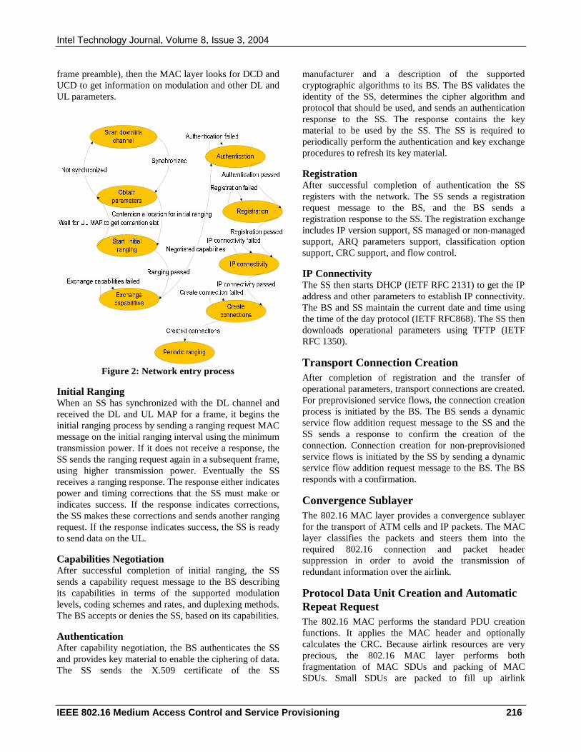
Intel Technology Journal, Volume 8, Issue 3, 2004
IEEE 802.16 Medium Access Control and Service Provisioning 216
frame preamble), then the MAC layer looks for DCD and UCD to get information on modulation and other DL and UL parameters.
Figure 2: Network entry process
Initial Ranging When an SS has synchronized with the DL channel and received the DL and UL MAP for a frame, it begins the initial ranging process by sending a ranging request MAC message on the initial ranging interval using the minimum transmission power. If it does not receive a response, the SS sends the ranging request again in a subsequent frame, using higher transmission power. Eventually the SS receives a ranging response. The response either indicates power and timing corrections that the SS must make or indicates success. If the response indicates corrections, the SS makes these corrections and sends another ranging request. If the response indicates success, the SS is ready to send data on the UL.
Capabilities Negotiation After successful completion of initial ranging, the SS sends a capability request message to the BS describing its capabilities in terms of the supported modulation levels, coding schemes and rates, and duplexing methods. The BS accepts or denies the SS, based on its capabilities.
Authentication After capability negotiation, the BS authenticates the SS and provides key material to enable the ciphering of data. The SS sends the X.509 certificate of the SS
manufacturer and a description of the supported cryptographic algorithms to its BS. The BS validates the identity of the SS, determines the cipher algorithm and protocol that should be used, and sends an authentication response to the SS. The response contains the key material to be used by the SS. The SS is required to periodically perform the authentication and key exchange procedures to refresh its key material.
Registration After successful completion of authentication the SS registers with the network. The SS sends a registration request message to the BS, and the BS sends a registration response to the SS. The registration exchange includes IP version support, SS managed or non-managed support, ARQ parameters support, classification option support, CRC support, and flow control.
IP Connectivity The SS then starts DHCP (IETF RFC 2131) to get the IP address and other parameters to establish IP connectivity. The BS and SS maintain the current date and time using the time of the day protocol (IETF RFC868). The SS then downloads operational parameters using TFTP (IETF RFC 1350).
Transport Connection Creation After completion of registration and the transfer of operational parameters, transport connections are created. For preprovisioned service flows, the connection creation process is initiated by the BS. The BS sends a dynamic service flow addition request message to the SS and the SS sends a response to confirm the creation of the connection. Connection creation for non-preprovisioned service flows is initiated by the SS by sending a dynamic service flow addition request message to the BS. The BS responds with a confirmation.
Convergence Sublayer The 802.16 MAC layer provides a convergence sublayer for the transport of ATM cells and IP packets. The MAC layer classifies the packets and steers them into the required 802.16 connection and packet header suppression in order to avoid the transmission of redundant information over the airlink.
Protocol Data Unit Creation and Automatic Repeat Request The 802.16 MAC performs the standard PDU creation functions. It applies the MAC header and optionally calculates the CRC. Because airlink resources are very precious, the 802.16 MAC layer performs both fragmentation of MAC SDUs and packing of MAC SDUs. Small SDUs are packed to fill up airlink

Intel Technology Journal, Volume 8, Issue 3, 2004
IEEE 802.16 Medium Access Control and Service Provisioning 217
allocations and large SDUs are fragmented when they don’t fit into an airlink allocation. MAC PDUs may be concatenated into bursts having the same modulation and coding.
Figure 3: PDU and SDU in protocol stack
ARQ processing is the process of retransmitting MAC SDU blocks (“ARQ blocks”) that have been lost or garbled. The 802.16 MAC uses a simple sliding window-based approach, where the transmitter can transmit up to a negotiated number of blocks without receiving an acknowledgement. The receiver sends acknowledgement or negative acknowledgement messages to indicate to the transmitter which SDU blocks have successfully been received and which have been lost. The transmitter retransmits blocks that were lost and moves the sliding window forward when SDU blocks are acknowledged to have been received.
Service Classes The 802.16 MAC provides QoS differentiation for different types of applications that might operate over 802.16 networks. The 802.16 standard defines the following types of services:
! Unsolicited Grant Services (UGS): UGS is designed to support Constant Bit Rate (CBR) services, such as T1/E1 emulation, and Voice Over IP (VoIP) without silence suppression.
! Real-Time Polling Services (rtPS): rtPS is designed to support real-time services that generate variable size data packets on a periodic basis, such as MPEG video or VoIP with silence suppression.
! Non-Real-Time Polling Services (nrtPS): nrtPS is designed to support non-real-time services that require variable size data grant burst types on a regular basis.
! Best Effort (BE) Services: BE services are typically provided by the Internet today for Web surfing.
Each SS to BS connection is assigned a service class as part of the creation of the connection. When packets are classified in the convergence sublayer, the connection into which they are placed is chosen based on the type of QoS guarantees that are required by the application. Figure 4 depicts the 802.16 QoS mechanism in supporting multimedia services, including TDM voice, VoIP, video streaming, TFTP, HTTP, and e-mail.
Figure 4: QoS mechanism for multimedia services
There are two types of polling mechanisms:
Unicast: When an SS is polled individually, it is allocated bandwidth to send bandwidth request messages.
Contention-based: Contention-based bandwidth request is used when insufficient bandwidth is available to individually poll many inactive SS’s. The allocation is multicast or broadcast to a group of SS’s that have to contend for the opportunity to send bandwidth requests.
Scheduling and Link Adaptation The goal of scheduling and link adaptation is to provide the desired QoS treatment to the traffic traversing the airlink, while optimally utilizing the resources of the airlink. Scheduling in the 802.16 MAC is divided into two related scheduling tasks: scheduling the usage of the
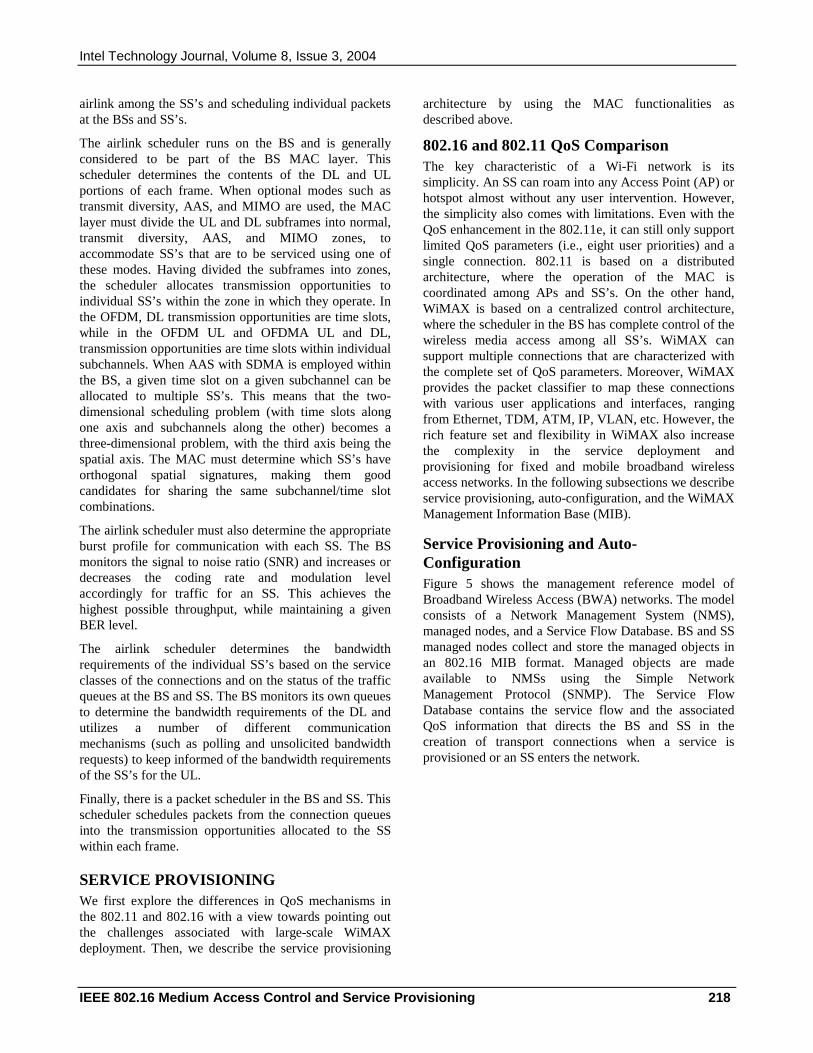
Intel Technology Journal, Volume 8, Issue 3, 2004
IEEE 802.16 Medium Access Control and Service Provisioning 218
airlink among the SS’s and scheduling individual packets at the BSs and SS’s.
The airlink scheduler runs on the BS and is generally considered to be part of the BS MAC layer. This scheduler determines the contents of the DL and UL portions of each frame. When optional modes such as transmit diversity, AAS, and MIMO are used, the MAC layer must divide the UL and DL subframes into normal, transmit diversity, AAS, and MIMO zones, to accommodate SS’s that are to be serviced using one of these modes. Having divided the subframes into zones, the scheduler allocates transmission opportunities to individual SS’s within the zone in which they operate. In the OFDM, DL transmission opportunities are time slots, while in the OFDM UL and OFDMA UL and DL, transmission opportunities are time slots within individual subchannels. When AAS with SDMA is employed within the BS, a given time slot on a given subchannel can be allocated to multiple SS’s. This means that the two-dimensional scheduling problem (with time slots along one axis and subchannels along the other) becomes a three-dimensional problem, with the third axis being the spatial axis. The MAC must determine which SS’s have orthogonal spatial signatures, making them good candidates for sharing the same subchannel/time slot combinations.
The airlink scheduler must also determine the appropriate burst profile for communication with each SS. The BS monitors the signal to noise ratio (SNR) and increases or decreases the coding rate and modulation level accordingly for traffic for an SS. This achieves the highest possible throughput, while maintaining a given BER level.
The airlink scheduler determines the bandwidth requirements of the individual SS’s based on the service classes of the connections and on the status of the traffic queues at the BS and SS. The BS monitors its own queues to determine the bandwidth requirements of the DL and utilizes a number of different communication mechanisms (such as polling and unsolicited bandwidth requests) to keep informed of the bandwidth requirements of the SS’s for the UL.
Finally, there is a packet scheduler in the BS and SS. This scheduler schedules packets from the connection queues into the transmission opportunities allocated to the SS within each frame.
SERVICE PROVISIONING We first explore the differences in QoS mechanisms in the 802.11 and 802.16 with a view towards pointing out the challenges associated with large-scale WiMAX deployment. Then, we describe the service provisioning
architecture by using the MAC functionalities as described above.
802.16 and 802.11 QoS Comparison The key characteristic of a Wi-Fi network is its simplicity. An SS can roam into any Access Point (AP) or hotspot almost without any user intervention. However, the simplicity also comes with limitations. Even with the QoS enhancement in the 802.11e, it can still only support limited QoS parameters (i.e., eight user priorities) and a single connection. 802.11 is based on a distributed architecture, where the operation of the MAC is coordinated among APs and SS’s. On the other hand, WiMAX is based on a centralized control architecture, where the scheduler in the BS has complete control of the wireless media access among all SS’s. WiMAX can support multiple connections that are characterized with the complete set of QoS parameters. Moreover, WiMAX provides the packet classifier to map these connections with various user applications and interfaces, ranging from Ethernet, TDM, ATM, IP, VLAN, etc. However, the rich feature set and flexibility in WiMAX also increase the complexity in the service deployment and provisioning for fixed and mobile broadband wireless access networks. In the following subsections we describe service provisioning, auto-configuration, and the WiMAX Management Information Base (MIB).
Service Provisioning and Auto-Configuration Figure 5 shows the management reference model of Broadband Wireless Access (BWA) networks. The model consists of a Network Management System (NMS), managed nodes, and a Service Flow Database. BS and SS managed nodes collect and store the managed objects in an 802.16 MIB format. Managed objects are made available to NMSs using the Simple Network Management Protocol (SNMP). The Service Flow Database contains the service flow and the associated QoS information that directs the BS and SS in the creation of transport connections when a service is provisioned or an SS enters the network.
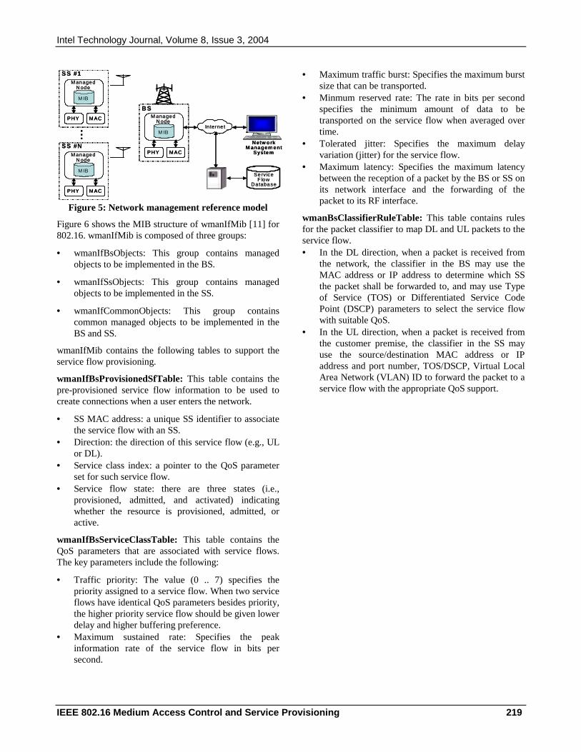
Intel Technology Journal, Volume 8, Issue 3, 2004
IEEE 802.16 Medium Access Control and Service Provisioning 219
S S #1M anaged
N ode
M IB
M AC
...
B S
Netw orkM anagem ent
System
In ternet
ServiceF low
Database
P HY M anagedN ode
M IB
M ACP HYS S #N
M anagedN ode
M IB
M ACP HY
S S #1M anaged
N ode
M IBM IB
M ACM AC
...
B S
Netw orkM anagem ent
System
In ternet
ServiceF low
Database
P HYP HY M anagedN ode
M IBM IB
M ACM ACP HYP HYS S #N
M anagedN ode
M IBM IB
M ACM ACP HYP HY
Figure 5: Network management reference model
Figure 6 shows the MIB structure of wmanIfMib [11] for 802.16. wmanIfMib is composed of three groups:
• wmanIfBsObjects: This group contains managed objects to be implemented in the BS.
• wmanIfSsObjects: This group contains managed objects to be implemented in the SS.
• wmanIfCommonObjects: This group contains common managed objects to be implemented in the BS and SS.
wmanIfMib contains the following tables to support the service flow provisioning.
wmanIfBsProvisionedSfTable: This table contains the pre-provisioned service flow information to be used to create connections when a user enters the network.
• SS MAC address: a unique SS identifier to associate the service flow with an SS.
• Direction: the direction of this service flow (e.g., UL or DL).
• Service class index: a pointer to the QoS parameter set for such service flow.
• Service flow state: there are three states (i.e., provisioned, admitted, and activated) indicating whether the resource is provisioned, admitted, or active.
wmanIfBsServiceClassTable: This table contains the QoS parameters that are associated with service flows. The key parameters include the following:
• Traffic priority: The value (0 .. 7) specifies the priority assigned to a service flow. When two service flows have identical QoS parameters besides priority, the higher priority service flow should be given lower delay and higher buffering preference.
• Maximum sustained rate: Specifies the peak information rate of the service flow in bits per second.
• Maximum traffic burst: Specifies the maximum burst size that can be transported.
• Minmum reserved rate: The rate in bits per second specifies the minimum amount of data to be transported on the service flow when averaged over time.
• Tolerated jitter: Specifies the maximum delay variation (jitter) for the service flow.
• Maximum latency: Specifies the maximum latency between the reception of a packet by the BS or SS on its network interface and the forwarding of the packet to its RF interface.
wmanBsClassifierRuleTable: This table contains rules for the packet classifier to map DL and UL packets to the service flow. • In the DL direction, when a packet is received from
the network, the classifier in the BS may use the MAC address or IP address to determine which SS the packet shall be forwarded to, and may use Type of Service (TOS) or Differentiated Service Code Point (DSCP) parameters to select the service flow with suitable QoS.
• In the UL direction, when a packet is received from the customer premise, the classifier in the SS may use the source/destination MAC address or IP address and port number, TOS/DSCP, Virtual Local Area Network (VLAN) ID to forward the packet to a service flow with the appropriate QoS support.
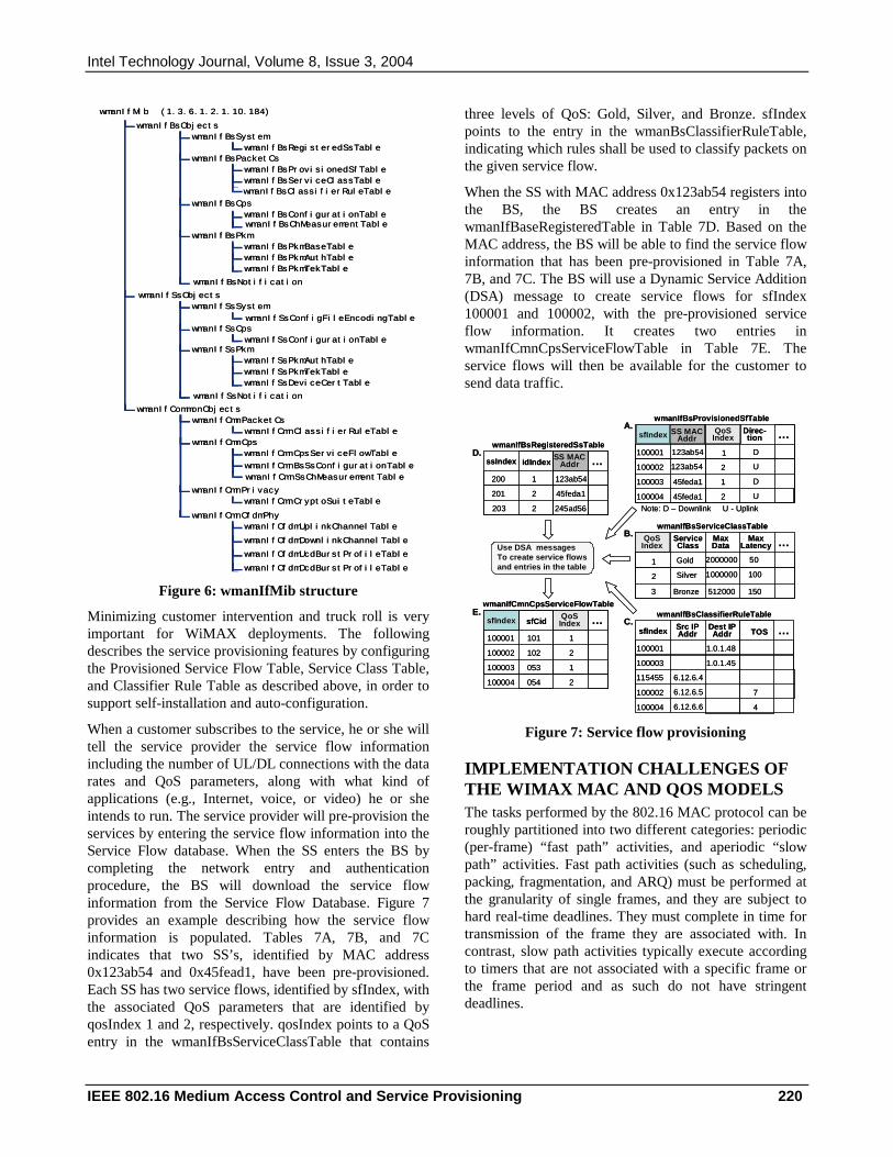
Intel Technology Journal, Volume 8, Issue 3, 2004
IEEE 802.16 Medium Access Control and Service Provisioning 220
wmanIfMib (1.3.6.1.2.1.10.184)
wmanIfBsObjects
wmanIfBsSystem
wmanIfBsRegisteredSsTable
wmanIfBsPacketCs
wmanIfBsProvisionedSfTable
wmanIfBsServiceClassTable
wmanIfBsCps
wmanIfBsPkm
wmanIfBsPkmBaseTable
wmanIfBsPkmAuthTable
wmanIfBsPkmTekTable
wmanIfSsObjects
wmanIfSsSystem
wmanIfSsCps
wmanIfSsConfigurationTablewmanIfSsPkm
wmanIfSsPkmAuthTable
wmanIfSsPkmTekTable
wmanIfSsDeviceCertTable
wmanIfCommonObjects
wmanIfCmnPacketCs
wmanIfCmnClassifierRuleTable
wmanIfCmnCps
wmanIfCmnSsChMeasurementTable
wmanIfCmnBsSsConfigurationTable
wmanIfCmnPrivacy
wmanIfCmnCryptoSuiteTable
wmanIfCmnCpsServiceFlowTable
wmanIfCmnOfdmPhy
wmanIfOfdmUplinkChannelTable
wmanIfOfdmUcdBurstProfileTable
wmanIfOfdmDownlinkChannelTable
wmanIfOfdmDcdBurstProfileTable
wmanIfBsClassifierRuleTable
wmanIfSsConfigFileEncodingTable
wmanIfBsNotification
wmanIfBsChMeasurementTablewmanIfBsConfigurationTable
wmanIfSsNotification
Figure 6: wmanIfMib structure
Minimizing customer intervention and truck roll is very important for WiMAX deployments. The following describes the service provisioning features by configuring the Provisioned Service Flow Table, Service Class Table, and Classifier Rule Table as described above, in order to support self-installation and auto-configuration.
When a customer subscribes to the service, he or she will tell the service provider the service flow information including the number of UL/DL connections with the data rates and QoS parameters, along with what kind of applications (e.g., Internet, voice, or video) he or she intends to run. The service provider will pre-provision the services by entering the service flow information into the Service Flow database. When the SS enters the BS by completing the network entry and authentication procedure, the BS will download the service flow information from the Service Flow Database. Figure 7 provides an example describing how the service flow information is populated. Tables 7A, 7B, and 7C indicates that two SS’s, identified by MAC address 0x123ab54 and 0x45fead1, have been pre-provisioned. Each SS has two service flows, identified by sfIndex, with the associated QoS parameters that are identified by qosIndex 1 and 2, respectively. qosIndex points to a QoS entry in the wmanIfBsServiceClassTable that contains
three levels of QoS: Gold, Silver, and Bronze. sfIndex points to the entry in the wmanBsClassifierRuleTable, indicating which rules shall be used to classify packets on the given service flow.
When the SS with MAC address 0x123ab54 registers into the BS, the BS creates an entry in the wmanIfBaseRegisteredTable in Table 7D. Based on the MAC address, the BS will be able to find the service flow information that has been pre-provisioned in Table 7A, 7B, and 7C. The BS will use a Dynamic Service Addition (DSA) message to create service flows for sfIndex 100001 and 100002, with the pre-provisioned service flow information. It creates two entries in wmanIfCmnCpsServiceFlowTable in Table 7E. The service flows will then be available for the customer to send data traffic.
sfIndex …
wmanIfBsProvisionedSfTable
wmanIfBsServiceClassTable
wmanIfBsClassifierRuleTable
wmanIfBsRegisteredSsTable
wmanIfCmnCpsServiceFlowTable
Use DSA messagesTo create service flowsand entries in the table
100001 D
U
D
U
1
2
1
2
2
1
123ab54
123ab54
45feda1
45feda1
100002
100003
100004
100001
100003
1.0.1.48
1.0.1.45
100002
100004
7
4
100001
100002
100003
100004
101
102
053
054
TOS
Gold
Silver
Note: D – Downlink U - Uplink
SS MACAddr
QoSIndex
QoSIndex
ServiceClass
MaxData
MaxLatency
Direc-tion
…
sfIndex Src IPAddr
Dest IPAddr …
ssIndex …200 1
2
123ab54
45feda1201
idIndexSS MAC
Addr
sfIndex …1
2
sfCidQoSIndex
2
1
2000000
1000000
50
100
3 Bronze 512000 150
203 2 245ad56
115455 6.12.6.4
6.12.6.5
6.12.6.6
A.
B.
C.
D.
E.
Figure 7: Service flow provisioning
IMPLEMENTATION CHALLENGES OF THE WIMAX MAC AND QOS MODELS The tasks performed by the 802.16 MAC protocol can be roughly partitioned into two different categories: periodic (per-frame) “fast path” activities, and aperiodic “slow path” activities. Fast path activities (such as scheduling, packing, fragmentation, and ARQ) must be performed at the granularity of single frames, and they are subject to hard real-time deadlines. They must complete in time for transmission of the frame they are associated with. In contrast, slow path activities typically execute according to timers that are not associated with a specific frame or the frame period and as such do not have stringent deadlines.

Intel Technology Journal, Volume 8, Issue 3, 2004
IEEE 802.16 Medium Access Control and Service Provisioning 221
The two categories of tasks described above interact in that the slow path activities described above typically dictate the mode of operation of the fast path activities. For instance, SS registration and association with a BS, which occurs through the exchange of several messages, results in the creation of several connections and associated state between the SS and BS. These connections can include state to be tracked in the fast path such as fragmentation status, ARQ retransmissions, and packing.
In addition to supporting the QoS and MAC functionality described above, a set of virtualization challenges are faced by 802.16 MAC implementers as well. Specifically, it is expected that at system setup time it will be possible to configure single systems to treat multiple air channels as separate MAC instances. Thus a single BS (and associated MAC implementation) might for example utilize two 10 MHz channels in parallel as two separate MAC instances. This type of virtualization is necessary because the usage and allocation of available air bandwidth is highly dependent on carrier policies, system loading, and radio environment.
Supporting virtualization of the MAC layer has subtle implications for 802.16 MAC implementation. Gross attributes of system design such as total air bandwidth, and thus the above-MAC data rate (Mbps) and packet rate (PPS), is unchanged. Similarly, very fine-grained details, such as state machines for connection setup or for packing CS SDUs into a MAC PDU, remain the same. However, virtualization affects intermediate-level MAC abstracts, in that MAC state machines that deal with states such as the list of authenticated SS’s, or whether admission control can allow another bandwidth request, must now be virtualized so that a set of independent instances of each of these state machines must be executed and coordinated with each other. Furthermore, PHY indications must be provided such that frames from separate bands can be distinguished and delivered to the correct set of state machine instantiations for processing. Finally, the multiple instantiations, while independent from the point of view of shared state, are all executing on the same hardware, and as such care must be taken to ensure that MAC timeliness deadlines are still met for all state machine instances.
In addition to virtualization, another key architectural feature that must be supported by MAC implementations is extensibility. Extensibility, in terms of differentiating features such as alternative QoS scheduling algorithms, which may not be present in the base implementation of the MAC, is a second key challenge for MAC implementers. Extensibility is an important feature of the MAC protocol in that it is expected that BS manufacturers along with their customers will desire the
ability to easily customize the scheduler and other aspects of the MAC to differentiate their offerings from others. The 802.16 leaves a wide variety of options and functionality up to the implementer to determine how best to achieve a robust service offering.
The following two sections review the implementation challenges discussed above in the context of two processor architectures: the Intel IXP Network processor architecture, which utilizes core-multiprocessing and hardware threading support, and the Intel Architecture Pentium® M general-purpose processor architecture.
IXP Implementation Intel IXP network processors are especially suited for implementing high-density networking-related applications like access points, routers, and gateways. It is also a natural choice for WiMAX BSs. (It may also be used for SS’s playing the role of residential routing gateways). While the BS feature set is user-specific, the 802.16 MAC software is one of the most important BS components. The provided MAC software is designed to cooperate seamlessly with other ready-to-use IXP library routines, available with the IXA Software Development Kit (SDK) tool chain. Therefore it is easy to combine the MAC with chosen IXA SDK forwarding modules, be they IPv4, IPv6, or Multiprotocol Label Switching (MPLS). Moreover, a rich choice of network access interfaces is supported, e.g., Ethernet (100M, 1G, 10G), ATM (including TM4.1), and Packet Over SONET (POS).
Figure 8 shows a sample WiMAX BS software partitioning. The fast path activities are often referred to as Data Plane (DP) activities, and slow path activities are known as Control Plane (CP) activities. The CP-related code modules deal with policies, while the DP-related modules are concerned with execution. The CP sets control tables used by the DP.
An IXP network processor hosts both the DP modules and CP modules. As shown in the figure, the DP modules run partly on IXP microengines (and are frequently referred to as “microblocks”) and partly on the IXP XScale® integrated control processor (the code directly cooperating with microblocks is called “core components”). The microblocks utilize hardware multithreading, while the XScale code uses an embedded
® Pentium is a registered trademark of Intel Corporation or its subsidiaries in the United States and other countries. ® XScale is a registered trademark of Intel Corporation and its subsidiaries in the United States and other countries.

Intel Technology Journal, Volume 8, Issue 3, 2004
IEEE 802.16 Medium Access Control and Service Provisioning 222
operating kernel (e.g., Linux* or VxWorks*) to work in multiprogramming mode. More information on the IXP hardware, software, and tools is available at the Intel web site [1]; see also the Intel Technology Journal [2], [3], [4], [5].
The IXP code is directly portable across the IXP 2xxx network processor range.
Figure 8: Sample WiMAX BS software partitioning
The DP part includes 802.16 MAC, including UL and DL schedulers, and typically also some forwarder module (e.g., IPv4 router with DiffServ support). From the RF side, it interfaces to the 802.16 PHY (OFDM, OFDMA), implementing baseband processing, using a so-called PHY Service Access Point Application Programming Interface (SAP API). From the network side, this may be, for example, a Gigabit Ethernet or ATM network, accessible via a CS API that is compliant with an IXA SDK framework. The interface to the CP is done using IXP shared memory.
Some of the tasks such as handling the MAC management messages are serviced either by the DP or CP, depending on their relative frequency. For example, the 802.16 DP will service Bandwidth Requests (in), ARQ (in, out), DL-MAP (out), UL-MAP (out), DCD/UCD (out), while the other MAC messages that are not time critical will be passed to the CP for processing. We call this class “signaling messages”; they are handled according to the state machines maintained by the CP.
The CP part contains the IXA SDK infrastructure code (implementing generic communication mechanisms between XScale and microengines), the core components, and Network Processing Forum (NPF)-style control API
* All other brands and names are the property of their respective owners.
(FAPI) [6]. The core components include MAC-related code, and also the code cooperating with the forwarder (so-called “slow path” implementation). On top of FAPI, there is the remaining CP software, including the MAC signaling stack, management and monitoring applications, etc. It is worth mentioning that it is possible to remote the FAPI to some external control processor, using the ForCES framework [7], Remote Procedure Call (RPC), or Common Object Request Broker Architecture (CORBA). For the WiMAX BS, the XScale processing power is adequate to run all the necessary CP software by itself, however.
The CP also controls the PHY hardware, via driver software that is accessed by using the FAPI.
IXP Data Flows Figure 8 also shows the data flows within the IXP network processor. The main data stream is transferred between the RF side and the external network. The IXP microblocks are responsible for handling this data stream. A part of the data stream (containing non time-critical MAC Management messages) terminates at the CP; it is handled by the 802.16 MAC signaling stack. Lastly, the CP management software sets or gets configuration and monitoring data (shared with microengines) using the FAPI.
CP-DP Cooperation The CP cooperates with the DP across the FAPI. The CP issues requests, which may convey configuration data, queries, or they may contain MAC Management messages (to be sent to a remote SS), and it receives responses to those requests and also asynchronous events (e.g., MAC Management messages coming from remote SS’s).
MAC-PHY Cooperation The MAC and PHY layers cooperate across the PHY SAP API. This interface enables a fast and low-latency exchange of traffic data between PHY and MAC, and also supports in-band PHY configuration (setting TX/RX Vector, a data structure equivalent to DL-MAP and UL-MAP, which has to be provided for the PHY frame after frame). The interface is asynchronous and supports multiple MAC instances, which enables parallel servicing of many transmission channels.
It is assumed that it is PHY that maintains precise time synchronization needed to transmit or receive a frame. MAC is loosely coupled with PHY over the PHY SAP API.
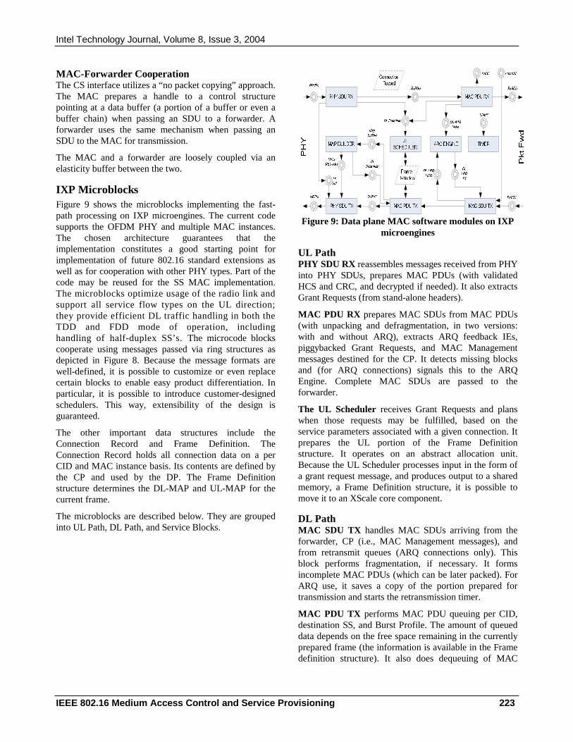
Intel Technology Journal, Volume 8, Issue 3, 2004
IEEE 802.16 Medium Access Control and Service Provisioning 223
MAC-Forwarder Cooperation The CS interface utilizes a “no packet copying” approach. The MAC prepares a handle to a control structure pointing at a data buffer (a portion of a buffer or even a buffer chain) when passing an SDU to a forwarder. A forwarder uses the same mechanism when passing an SDU to the MAC for transmission.
The MAC and a forwarder are loosely coupled via an elasticity buffer between the two.
IXP Microblocks Figure 9 shows the microblocks implementing the fast-path processing on IXP microengines. The current code supports the OFDM PHY and multiple MAC instances. The chosen architecture guarantees that the implementation constitutes a good starting point for implementation of future 802.16 standard extensions as well as for cooperation with other PHY types. Part of the code may be reused for the SS MAC implementation. The microblocks optimize usage of the radio link and support all service flow types on the UL direction; they provide efficient DL traffic handling in both the TDD and FDD mode of operation, including handling of half-duplex SS’s. The microcode blocks cooperate using messages passed via ring structures as depicted in Figure 8. Because the message formats are well-defined, it is possible to customize or even replace certain blocks to enable easy product differentiation. In particular, it is possible to introduce customer-designed schedulers. This way, extensibility of the design is guaranteed.
The other important data structures include the Connection Record and Frame Definition. The Connection Record holds all connection data on a per CID and MAC instance basis. Its contents are defined by the CP and used by the DP. The Frame Definition structure determines the DL-MAP and UL-MAP for the current frame.
The microblocks are described below. They are grouped into UL Path, DL Path, and Service Blocks.
Figure 9: Data plane MAC software modules on IXP microengines
UL Path PHY SDU RX reassembles messages received from PHY into PHY SDUs, prepares MAC PDUs (with validated HCS and CRC, and decrypted if needed). It also extracts Grant Requests (from stand-alone headers).
MAC PDU RX prepares MAC SDUs from MAC PDUs (with unpacking and defragmentation, in two versions: with and without ARQ), extracts ARQ feedback IEs, piggybacked Grant Requests, and MAC Management messages destined for the CP. It detects missing blocks and (for ARQ connections) signals this to the ARQ Engine. Complete MAC SDUs are passed to the forwarder.
The UL Scheduler receives Grant Requests and plans when those requests may be fulfilled, based on the service parameters associated with a given connection. It prepares the UL portion of the Frame Definition structure. It operates on an abstract allocation unit. Because the UL Scheduler processes input in the form of a grant request message, and produces output to a shared memory, a Frame Definition structure, it is possible to move it to an XScale core component.
DL Path MAC SDU TX handles MAC SDUs arriving from the forwarder, CP (i.e., MAC Management messages), and from retransmit queues (ARQ connections only). This block performs fragmentation, if necessary. It forms incomplete MAC PDUs (which can be later packed). For ARQ use, it saves a copy of the portion prepared for transmission and starts the retransmission timer.
MAC PDU TX performs MAC PDU queuing per CID, destination SS, and Burst Profile. The amount of queued data depends on the free space remaining in the currently prepared frame (the information is available in the Frame definition structure). It also does dequeuing of MAC
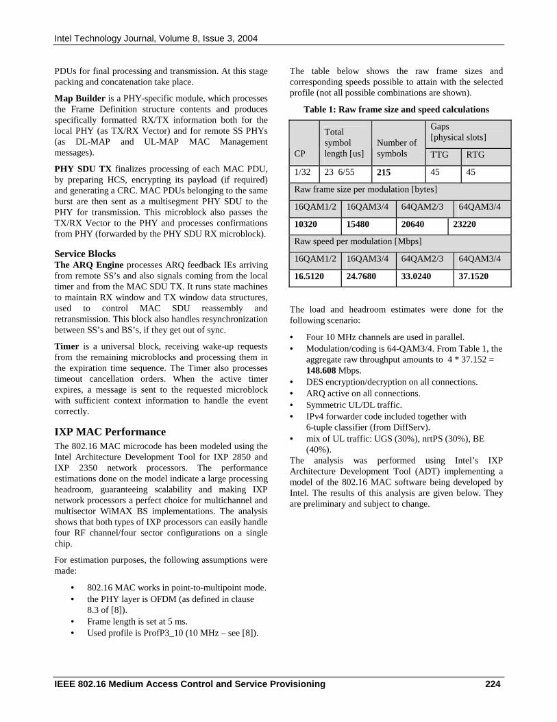
Intel Technology Journal, Volume 8, Issue 3, 2004
IEEE 802.16 Medium Access Control and Service Provisioning 224
PDUs for final processing and transmission. At this stage packing and concatenation take place.
Map Builder is a PHY-specific module, which processes the Frame Definition structure contents and produces specifically formatted RX/TX information both for the local PHY (as TX/RX Vector) and for remote SS PHYs (as DL-MAP and UL-MAP MAC Management messages).
PHY SDU TX finalizes processing of each MAC PDU, by preparing HCS, encrypting its payload (if required) and generating a CRC. MAC PDUs belonging to the same burst are then sent as a multisegment PHY SDU to the PHY for transmission. This microblock also passes the TX/RX Vector to the PHY and processes confirmations from PHY (forwarded by the PHY SDU RX microblock).
Service Blocks The ARQ Engine processes ARQ feedback IEs arriving from remote SS’s and also signals coming from the local timer and from the MAC SDU TX. It runs state machines to maintain RX window and TX window data structures, used to control MAC SDU reassembly and retransmission. This block also handles resynchronization between SS’s and BS’s, if they get out of sync.
Timer is a universal block, receiving wake-up requests from the remaining microblocks and processing them in the expiration time sequence. The Timer also processes timeout cancellation orders. When the active timer expires, a message is sent to the requested microblock with sufficient context information to handle the event correctly.
IXP MAC Performance The 802.16 MAC microcode has been modeled using the Intel Architecture Development Tool for IXP 2850 and IXP 2350 network processors. The performance estimations done on the model indicate a large processing headroom, guaranteeing scalability and making IXP network processors a perfect choice for multichannel and multisector WiMAX BS implementations. The analysis shows that both types of IXP processors can easily handle four RF channel/four sector configurations on a single chip.
For estimation purposes, the following assumptions were made:
• 802.16 MAC works in point-to-multipoint mode. • the PHY layer is OFDM (as defined in clause
8.3 of [8]). • Frame length is set at 5 ms. • Used profile is ProfP3_10 (10 MHz – see [8]).
The table below shows the raw frame sizes and corresponding speeds possible to attain with the selected profile (not all possible combinations are shown).
Table 1: Raw frame size and speed calculations
Gaps [physical slots]
CP
Total symbol length [us]
Number of symbols TTG RTG
1/32 23 6/55 215 45 45
Raw frame size per modulation [bytes]
16QAM1/2 16QAM3/4 64QAM2/3 64QAM3/4
10320 15480 20640 23220
Raw speed per modulation [Mbps]
16QAM1/2 16QAM3/4 64QAM2/3 64QAM3/4
16.5120 24.7680 33.0240 37.1520
The load and headroom estimates were done for the following scenario:
• Four 10 MHz channels are used in parallel. • Modulation/coding is 64-QAM3/4. From Table 1, the
aggregate raw throughput amounts to 4 * 37.152 = 148.608 Mbps.
• DES encryption/decryption on all connections. • ARQ active on all connections. • Symmetric UL/DL traffic. • IPv4 forwarder code included together with
6-tuple classifier (from DiffServ). • mix of UL traffic: UGS (30%), nrtPS (30%), BE
(40%). The analysis was performed using Intel’s IXP Architecture Development Tool (ADT) implementing a model of the 802.16 MAC software being developed by Intel. The results of this analysis are given below. They are preliminary and subject to change.

Intel Technology Journal, Volume 8, Issue 3, 2004
IEEE 802.16 Medium Access Control and Service Provisioning 225
Table 2: Summary of microengine utilization for IXP2850 (at 1.4 GHz) and IXP2350 (at 900 MHz)
IXP2850 (1.4 GHz)
IXP2350 (900 MHz)
Internal Bus Bandwidth
3% 7%
Memory Bus Bandwidth
7% 19%
Microengine (ME) Utilization
4% 9%
Crypto Unit Utilization
1% n/a1
Table 3: A preliminary code space and local memory occupancy estimations for MEv2
Micro engine
Num. of Threads
Num. of Instr.
Local Mem Words
ME #1 6 (2 free) 5350 (34% free)
480 (53 % free)
ME #2 8 (0 free) 6100 (25% free)
576 (43% free)
ME #3 8 (0 free) 5120 (37% free)
530 (48% free)
ME #4 6 (2 free) 5100 (37% free)
96 (90% free)
Intel Architecture MAC Implementation Goals The 802.16 specification defines a complex, powerful MAC protocol for achieving high bandwidth and robust service offerings. In addition to the MAC features and functionality described in the first part of this paper, the following design considerations were used in architecting the Intel Architecture BS MAC implementation of 802.16 with the OFDMA PHY. Extensibility, as described above was a primary requirement in the Intel Architecture BS
1 The current ADT version does not support IXP2350 crypto unit modeling. It is assumed that the crypto unit will handle the expected load, since its bandwidth is 200 Mbps.
MAC implementation. Scalability, both in the design of the software MAC as well as in the BS design itself, was another key requirement. Portability of the MAC implementation was also a key design consideration, which goes hand in hand with scalability. A portable MAC implementation should be able to execute on any of the wide range of Intel architecture and XScale architecture general-purpose processors. This section describes in detail the scalability and portability requirements that drove the Intel Architecture MAC design, while the following section describes the architectural approach chosen to satisfy the requirements given here and in the introduction to the Implementation Challenges section.
Scalability Scalability is a key feature of the MAC in that it is envisioned that BSs will have a wide variety of physical configurations, ranging from “pico” BS’s to “macro” systems.
In this context, a pico BS might be deployed mounted on a pole with a small, single sector and single omnidirectional antenna, perhaps with limited bandwidth and tight power and heat limitations, and subject to outdoor environment-level temperatures. At the other extreme, a heavy iron BS might be rack mounted, support multiple sectors, have many antennae, and be in an environmentally controlled cabinet or small building, with a large antenna tower connected to it.
As such, it must be possible for the MAC software implementation to be usable with the wide range of processor performance levels available with general-purpose processors such as Intel Architecture processors. The system must be implemented such that performance scales in a predictable fashion with processor performance, allowing appropriate processors to be chosen for executing the MAC software.
Portability Portability is a key feature of the Intel Architecture MAC implementation for similar reasons. The wide range of performance and price points likely to be associated with WiMAX BSs creates the need to easily choose different processors based on power, price, heat, and performance metrics. The Intel Architecture MAC design takes this feature as a primary goal, providing a complete and robust MAC offering while at the same time allowing it to be ported across the range of Intel general-purpose

Intel Technology Journal, Volume 8, Issue 3, 2004
IEEE 802.16 Medium Access Control and Service Provisioning 226
processor architectures, including Pentium® M, Pentium 4, Xeon®, XScale, and Celeron®.
Intel Architecture MAC Features and Design As explained previously, the tasks that make up 802.16 can be divided into two categories: time-critical, periodic operations that must occur on every frame, and slower, less demanding aperiodic operations that typically operate over the duration of several frames. In order to support this mixture of processing tasks, the Intel Architecture implementation of 802.16 uses a multilevel hard real-time priority-based scheduling system. The scheduling system utilizes three priority levels of events: high, medium, and low. High-priority events are those events that must always be serviced in a timely fashion, and must not be executed past their deadline or the basic functionality of the MAC will be compromised. Medium-priority events are events that have strict time requirements, but if their deadlines are missed they may be skipped without causing a catastrophic failure. Finally, low-priority events are events that typically do not have strict processing requirements associated with them; they are processed on a best-effort basis whenever processing time is available.
All functionality involved in 802.16 MAC processing is implemented as one or more events, all of which fall into one of three categories: periodic events, protocol-driven events, and I/O-driven events. Periodic events are events that occur with a known and fixed regularity. For example, delivery of a ready frame by the MAC software to the PHY device driver for transmission is a high-priority event that occurs exactly once every frame period (typically 2.5-5 ms). Generating the UL-MAP that is part of the ready frame (by the UL scheduler) is another periodic high-priority event that occurs exactly once every frame period.
Protocol-driven events are events that are added to one of the priority queues based on external stimuli associated with the 802.16 MAC itself. For example, reception of a DSA-REQ message from an SS results in an event being
® Pentium is a registered trademark of Intel Corporation or its subsidiaries in the United States and other countries. ® Xeon is a registered trademark of Intel Corporation or its subsidiaries in the United States and other countries. ® Celeron is a registered trademark of Intel Corporation or its subsidiaries in the United States and other countries.
added to the low-priority queue to process the message (by invoking the QoS admission control event handler).
I/O-driven events are events that are added to one of the priority queues based on reception of I/O of some sort. Thus, notification by the 802.16 PHY that a new UL frame has been fully received results in an event being added to the medium-priority event queue for parsing of the received frame. Similarly, delivery of an Ethernet packet to the packet convergence sublayer results in an event being queued to the low-priority event queue for classification of the Ethernet frame into a per-CID queue.
All events have associated with them an earliest acceptable start time and a deadline time. If the associated event handler is invoked within this time interval it runs to completion, with medium- and low-priority event handlers always being implemented such that they have relatively small run times (perhaps resulting in scheduling of another follow-up event to continue processing later). If an event handler is not executed before its deadline, it instead will have a special late invocation call made that allows it to triage the missed event as best as possible.
The combination of event priority levels and controlled execution times allows the entire system to scale in a predictable, controlled fashion. Low-priority events, such as handling of newly received Ethernet frames or negotiating a request to set up a new connection, will never cause the system as a whole to miss high-priority event deadlines such as frame transmission times. This ensures that the system will always function correctly no matter what the maximum load, dropping low-priority traffic rather than becoming unsynchronized with the PHY, for instance. Conversely, as available processing power is increased, the system can scale to handle more and more medium- and low-priority events, thus being scalable to higher bandwidth configurations through the use of more powerful processors. The need for scalability of the 802.16 MAC is one of the key challenges identified in the implementation of this protocol, and the use of an event-based, real-time-scheduled system is a powerful and flexible method for achieving such scalability.
The use of an event-based system with the associated event handlers allows for great flexibility in implementation. Each event handler can be customized in its implementation, and as long as the specified pre- and post-conditions are met, along with the maximum execution time, the system implementation will work correctly. This predictable execution behavior, event-based system, and flexibility of the system allows the virtualization requirement to be easily met, because the events and associated state machines for the MAC can be
Intel Technology Journal, Volume 8, Issue 3, 2004
IEEE 802.16 Medium Access Control and Service Provisioning 227
multi-instanced in order to utilize multiple virtual MACs in support of multiple air channels.
The requirement of portability in this implementation is achieved through the selection of programming language for the entire implementation, which is ANSI C. Furthermore, the implementation is implemented in an endian-neutral fashion and only uses explicitly sized types. This makes it very simple for Telecommunications Equipment Manufacturers (TEMs) or carrier programmers to understand the existing code and port it across the range of Intel architecture general-purpose processors to suit their heat, price, and performance needs. Furthermore, the use of event handlers with known pre- and post-conditions and maximum execution periods, along with the use of ANSI C, allows for simple extensibility and customization of the 802.16 MAC. Thus the key challenge of extensibility is met and the goal of portability is achieved in the Intel Architecture-based implementation while still providing a complete and robust MAC implementation.
CONCLUSION The IEEE 802.16 is a very complicated standard, featuring high adaptiveness to maximize airlink usage; therefore, it requires sophisticated algorithms. At the same time, its implementation should expose ease-of-use for users and provide adequate QoS. Consequently, the 802.16 MAC poses significant challenges to the BS software implementer. Hard real-time deadlines must be met while still maintaining high throughput and predictable behavior. The two MAC implementations described above, which are available on Intel IXP network processors and Intel Architecture Pentium M processors, provide complete, robust implementations of the 802.16 specification, while at the same time also meet the additional stated goals of virtualization and extensibility presented in the introduction to this paper. The existence of two 802.16 BS MAC implementations enables equipment manufacturers to select the MAC software and associated processor architecture that best meets their power, price, portability, and performance needs.
ACKNOWLEDGMENTS The authors thank the reviewers: Al Dabagh Baraa, Shlomo Ovadia, and Henry Mitchel.
REFERENCES [1] For Intel IXA Network Processor resources: visit
http://developer.intel.com/design/network/products/npfamily/index.htm.
[2] Adiletta, Matthew et al., “The Next Generation of Intel IXP Network Processors,” in Intel Technology Journal, Volume 6, Issue 3, 2002.
[3] Naik, Uday et al., IXA Portability Framework: Preserving Software Investment in Network Processor Applications in Intel Technology Journal, Volume 6, Issue 3, 2002.
[4] Deval, Manasi et al., “Distributed Control Plane Architecture for Network Elements,” in Intel Technology Journal, Volume 7, Issue 4, 2003.
[5] Vinnakota, Bapi et al., “Scalable Intel IXA and its Building Blocks for Networking Platforms,” in Intel Technology Journal, Volume 7, Issue 4, 2003.
[6] FAPI Model & Usage Guidelines, June 10, 2004, npf2002.340.32 http://www.npforum.org/*
[7] IETF ForCES Working Group: http://www.ietf.org/html.charters/forces-charter.html.*
[8] IEEE™ P802.16-REVd/D5-2004: “Air Interface for Fixed Broadband Wireless Access Systems.”
[9] Govindan Nair, MAC 802.11 Point Coordination Function: http://www.intel.com/cd/ids/developer/asmo-na/eng/52768.htm
[10] Carl Eklund, Reger B. Marks, Kenneth L. Stanwood, and Stanley Wang, “IEEE™ Standard 802.16: Technical Overview of the Wireless MAN Air Interface for Broadband wireless Access,” IEEE™ Communications Magazine, June 2002.
[11] J. Chou, R. Reynold, V. Yanover, S. Eini, R. Selea, B. Moldoveanu, “MAC and PHY MIB for WirelessMAN and WirelessHUMAN BS and SS,” http://grouper.ieee.org/groups/802/16/mgt/contrib/C80216mgt-04_04.pdf*
[12] WiMAX PICS wiMAX Forum, “PICS for WirelessMAN-OFDM and WirelessHUMAN (-OFDM).”
[13] IEEE™ 802.11 “Wireless LAN Medium Access Control (MAC) and Physical (PHY) Layer Specifications.”
AUTHORS’ BIOGRAPHIES Govindan Nair is a senior software engineer in the Broadband Wireless Division where he is involved in software architecture, design and implementation of the 802.16 MAC and device drivers. Govindan co-authored PPP Static Interoperability Testing–Working Text (WT) 52 in DSL Forum, and he published the 802.11 MAC
Intel Technology Journal, Volume 8, Issue 3, 2004
IEEE 802.16 Medium Access Control and Service Provisioning 228
PCF implementation in the Intel Services Forum. Govindan received his M.S. degree in Computer Science from Manonmanium Sundaranar University, India. His e-mail is govindan.nair at intel.com.
Joey Chou is a customer architect for the Wireless Broadband Division. Joey is actively involved in the IEEE 802.16 Working Group and WiMAX Forum by leading the 802.16 MIB and Service Provisioning works, respectively. Joey was a key contributor to the VoDSL and VoIP standard works in the ATM Forum and DSL Forum, and was editor of the VoDSL Implementation Guideline and Interoperability Test Plan in the OpenVoB Forum. Prior to joining Intel in 1999, he worked at GTE, Siemens, AT&T, and Motorola on numerous telephony and narrowband and broadband wireless projects. He received a M.S. degree in Electrical Engineering from the Georgia Institute of Technology in 1985. His e-mail address is joey.chou at intel.com.
Tomasz Madejski received an M. Sc. degree from the Technical University of Gdansk, Poland in 1995. He joined Intel in 1999. He has 11 years of networking industry experience, mainly in the area of ATM. Currently, he is a senior architect in the Modular Communication Platform Division responsible for the design of an 802.16 MAC/scheduler implementation on the IXP2xxx line of network processors. His main interest areas are in quality of service in wireless networks and architecture of traffic schedulers. His e-mail is tomasz.madejski at intel.com.
Krzysztof Perycz is a senior staff architect on Intel’s MCPD team. He is currently responsible for 802.16 MAC/Scheduler design for the IXP2xxx series network processors. He holds an M.S. degree from the Technical University of Gdansk, Poland and has 30 years of industrial experience. He held various R&D positions at ZETO DP Center, Telecommunication Institute Poland, CrossComm Corp. and Olicom, before joining Intel in 1999. He authored nine papers, and holds one Polish patent and has filed for four US patents. His main professional interest focuses on telecommunication and computer science. His e-mail is krzysztof.perycz at intel.com.
David Putzolu is a senior staff architect in the Broadband Wireless Division where he is involved in software architecture and implementation of the 802.16 MAC. David’s areas of interest are wireless networks and modular software architectures for network equipment. David was principal editor and co-authored several Implementation Agreements in the Software Working Group of the Network Processing Forum, and he is co-chair of the IETF Forwarding and Control Element Separation Working Group. David received his M.S.
degree in Computer Science from the University of Illinois at Urbana-Champaign. His e-mail is david.putzolu at intel.com.
Jerry Sydir is a senior srchitect in the Broadband Wireless Division where he is involved in architecture of 802.16 baseband processors. Jerry has worked in a variety of hardware and software projects in the telecommunications area. Jerry received an M.S. degree in Systems Engineering and a B.S. degree in Computer Engineering from the Case Western Reserve University. Jerry’s professional interests include wireless communications, smart antenna technologies, and network protocols. His e-mail is jerry.sydir at intel.com.
Copyright © Intel Corporation 2004. This publication was downloaded from http://developer.intel.com/.
Legal notices at http://www.intel.com/sites/corporate/tradmarx.htm.

Multiple-Antenna Technology in WiMAX Systems 229
Multiple-Antenna Technology in WiMAX Systems
Atul Salvekar, Intel Communications Group, Intel Corporation Sumeet Sandhu, Corporate Technology Group, Intel Corporation
Qinghua Li, Corporate Technology Group, Intel Corporation Minh-Anh Vuong, Intel Communications Group, Intel Corporation
Xiaoshu Qian, Intel Communications Group, Intel Corporation
Index words: Alamouti, MIMO, diversity, AAS, WiMAX, broadband wireless
ABSTRACT
WiMAX is a wireless technology that provides broadband data at rates over 3 bits/second/Hz. In order to increase the range and reliability of WiMAX systems, the IEEE 802.16-2004 standard supports optional multiple-antenna techniques such as Alamouti Space-Time Coding (STC), Adaptive Antenna Systems (AAS) and Multiple-Input Multiple-Output (MIMO) systems. In this paper, we focus on techniques that do not require channel knowledge at the transmitter, which include both Alamouti STC and MIMO, but not AAS.
In the first half of the paper, we present simple diversity schemes that require only a single RF chain at the receiver. The performance of STC is compared with non-STC performance. Simulations show that STC buys 2-10 dB over a single antenna system, which can double the cell range and quadruple the cell coverage. For STC, multiple Radio Frequency (RF) chains are implemented at the Base Station (BS) to shift cost away from Subscriber Stations (SS), thus enabling market penetration for first-generation, high-performance IEEE 802.16-2004 networks. We then concentrate on other simple standard-compliant diversity schemes that require only a single receive chain at the SS: delay diversity and selection diversity.
The second half of the paper investigates standard-compliant MIMO techniques and proposes new non-standard advanced algorithms for open-loop MIMO. A novel space-frequency bit-interleaver that buys 2-4 dB over a frequency-only interleaver is presented. A 2x2 MIMO can double the throughput at a reduced range. An iterative receiver is introduced to recover range, which buys up to 5 dB with additional baseband complexity.
The intent of this paper is to provide an idea of the benefits of multiple antenna systems over single antenna systems in WiMAX-type deployments.
INTRODUCTION Wireless broadband promises to bring high-speed data to multitudes of people in various geographical locations where wired transmission is too costly, inconvenient, or unavailable. WiMAX is a technology devoted to making broadband wireless commercially available to the mass market by employing IEEE 802.16 standards-based technology. Other important wireless standards include IEEE 802.11, which is devoted to high-speed Local Area Networks (LANs) and IEEE 802.15, which is devoted to short-range Personal Area Networks (PANs).
WiMAX technology is based on the IEEE 802.16 specification of which IEEE 802.16-2004 and 802.16e amendment are Physical (PHY) layer specifications. The IEEE 802.16-2004 standard is primarily intended for stationary transmission while IEEE 802.16e amendment is intended primarily for both stationary and mobile deployments.
While there are multiple modulations defined in the IEEE 802.16 standards, in this paper, we examine Orthogonal Frequency Division Multiplexing (OFDM) because of OFDM’s robustness to multipath propagation and its ease for utilizing multiple antenna techniques [1]. Furthermore, we focus on IEEE 802.16-2004 technology as it has already been ratified.
IEEE 802.16-2004 currently supports several multiple-antenna options including Space-Time Codes (STC), Multiple-Input Multiple-Output (MIMO) antenna systems and Adaptive Antenna Systems (AAS).

Intel Technology Journal, Volume 8, Issue 3, 2004
Multiple-Antenna Technology in WiMAX Systems 230
There are several advantages to using multiple-antenna technology over single-antenna technology:
• Array Gain: This is the gain achieved by using multiple antennas so that the signal adds coherently.
• Diversity Gain: This is the gain achieved by utilizing multiple paths so that the probability that any one path is bad does not limit performance. Effectively, diversity gain refers to techniques at the transmitter or receiver to achieve multiple “looks” at the fading channel. These schemes improve performance by increasing the stability of the received signal strength in the presence of wireless signal fading. Diversity may be exploited in the spatial (antenna), temporal (time), or spectral (frequency) dimensions.
• Co-channel Interference Rejection (CCIR): This is the rejection of signals by making use of the different channel response of the interferers.
A common scheme that exhibits both array gain and diversity gain is maximal ratio combining: this combines multiple receive paths to maximize Signal to Noise Ratio (SNR). Selection diversity, on the other hand, primarily exhibits diversity gain; the signals are not combined; rather, the signal from the best antenna is chosen.
For AAS, multiple overlapped signals can be transmitted simultaneously using Space Division Multiple Access (SDMA), which is a technique that exploits the spatial dimension to transmit multiple beams that are spatially separated [3]. SDMA makes use of CCIR, diversity gain, and array gain. A good tutorial on AAS can be found in [3].
For MIMO systems, spatial multiplexing is often employed. Spatial multiplexing transmits coded data streams across different spatial domains. Some techniques, such as BLAST [6] do not require feedback, while others, such as vector coding on the modes of the channel [7], do. MIMO techniques can also make use of CCIR, diversity gain, and array gain. A form of transmission codes used in MIMO systems are STC. A good review of techniques for STC and MIMO can be found in [13 and 14].
The higher performance and lower interference capabilities of MIMO and AAS make them attractive over other high-rate techniques for WiMAX systems in costly, licensed bands.
For WiMAX, the simplest MIMO system is actually a Multiple-Input Single-Output (MISO) STC code called the Alamouti code. This requires two antennas at the
Base Station (BS). The Alamouti code provides maximal transmit diversity gain for two antennas [2]. Another transmit diversity scheme is cyclic delay diversity. A key advantage of transmit diversity is that it can be implemented at the BS, which can absorb higher costs of multiple antennas and associated RF chains. This shifts cost away from the SS, which enables faster market penetration of 802.16 products.
One of the many advantages of OFDM technology is the ease with which multiple-antenna techniques can be utilized to increase range and throughput (a system description is given below). Using this general system model, we show the primary advantage of OFDM systems over single-carrier systems in multipath propagation environments to explain why OFDM is conceptually less complex in AAS and MIMO systems. We then discuss a fixed point implementation of the Alamouti receiver. The fixed point simulations show several performance enhancements. Several practical aspects of the technology are also discussed. Next, we discuss several other simple diversity options, cyclic delay diversity and selection diversity, to improve system performance. We then describe more advanced schemes that could be used to achieve even higher throughput. We introduce open-loop techniques for multiple-antenna systems, which include standard compliant MIMO equalization, spatial-frequency interleaving, and iterative decoding. Simulation models are discussed that show large performance improvements.
SYSTEM DESCRIPTION We describe the Physical (PHY) layer of the general communication system. The performance of the PHY layer is strongly correlated to the overall system performance. However, higher-level entities such as Automatic Request (ARQ) for retransmission can also impact system performance.
A wireless environment suffers from multipath propagation. Multipath propagation, also known simply as multipath, is a condition where multiple reflections of the transmitter waveform arrive at the receiver at different times. This is shown in Figure 1, where a and b are the gains of the paths and τ1 and τ2 are the delays. The reflected path is actually the sum of multiple reflections from the obstruction, which causes fading. Multipath propagation induces Inter-Symbol Interference (ISI) which is traditionally compensated for by equalizers in single-carrier systems [4].

Intel Technology Journal, Volume 8, Issue 3, 2004
Multiple-Antenna Technology in WiMAX Systems 231
Figure 1: Conventional wireless system
Equalizers are computationally intense compared to the processing required in OFDM systems. Hence, OFDM is preferable in multipath propagation scenarios. A block diagram of OFDM is shown in Figure 2. As long as the CP, or Cyclic Prefix, is longer than the difference in multipath propagation arrival times, or multipath spread, an equalizer is not needed. The CP prepends the output of the Inverse Fast Fourier Transform (IFFT) with the last L samples of the IFFT output, where L is the length of the CP.
Figure 2: The OFDM system
For terminology, X[k] is the transmitted information symbol on subcarrier k. For subcarrier k, H[k] is the
scalar subcarrier response and its value is related to the FFT of the digitized channel response h(t), V[k] is the noise, and Y[k] is the output. The complete set of inputs {X[k]} is called the transmit OFDM symbol, and the set of demodulated signals {Y[k]} is called the receive OFDM symbol. On a subcarrier by subcarrier basis, there is no need for an equalizer.
Consider a MIMO system without noise as shown in Figure 4. In this figure, each ray corresponds to a multipath propagation channel. From the point of view of a subcarrier, each multipath propagation channel collapses to a single scalar tap. For subcarrier k, this can be expressed as shown in Figure 3 below.
∗
=
][
][
][][
][][
][][
][
][
][
2
1
3231
2221
1211
3
2
1
kX
kX
kHkH
kHkH
kHkH
kY
kY
kY
Figure 3: MIMO channel model
Transmitter
Receiver
X1[K]
X2[K]
Y1[K]
Y2[K]
Y3[K]
H11[K]
H12[K]
H21[K]
H31[K]
H22[K]
H23[K]
Figure 4: MIMO channel
In Figure 4, Yi[k] is the kth subcarrier output for receive antenna i, Hij[k] is the kth subcarrier gain from the jth transmit antenna to the ith receive antenna, and Xj[k] is the kth subcarrier input from antenna j.
In the single carrier case, each of the matrix elements would be multipath propagation channel responses. Conceptually, the signal processing is much more complicated; however, such systems can be simplified.
So, without loss of generality, rewriting the above equation, for an OFDM system would be
NXHY +∗= (eq. 1)
where Y, H, and X are the appropriate generalizations of the 2 transmit x 3 receive antenna system and N is the noise and interference. For general systems, H is an Mr by Mt matrix representing the number of transmit and receive antennas, respectively.
For an Additive White Gaussian Noise (AWGN) channel, the maximum achievable theoretical data rate of this system is given by the Shannon capacity formula [11]
( )*detlog HHICtMoBN
P+=
where P is the transmit power, No is the noise power spectral density, and B is the signal bandwidth. An Mt x Mr MIMO system can provide up to M=min (Mt, Mr) times the spectral efficiency of a 1x1 system. This linear relationship also holds true for outage capacity, which is equal to percentiles of the cumulative distribution function of C.
STC AND OTHER STANDARD-COMPLIANT DIVERSITY SCHEMES In order to increase the rate and range of the modem, there are several considerations. Generally, the BS can incur more cost and complexity than the SS, so multiple-antenna chains are a good option at the BS, which can then apply receiver diversity techniques. These

Intel Technology Journal, Volume 8, Issue 3, 2004
Multiple-Antenna Technology in WiMAX Systems 232
techniques include switched diversity and maximal ratio combining. To balance the link, the SS needs to have improved performance. Transmission diversity schemes are utilized at the BS that require only one receive antenna at the SS. Two transmit diversity schemes are cyclic delay diversity and Alamouti transmission. We focus on Alamouti transmission.
Alamouti Transmission The Alamouti transmission scheme is an STC in that it sends information on two transmit antennas and consists of two consecutive transmissions in time. Hence it transmits information in space and time.
In IEEE 802.16-2004 OFDM-256 the Alamouti code is applied to a specific subcarrier index k. For instance, suppose that in the uncoded system S1[k] and S2[k] are sent in the first and second OFDM symbol transmissions. The Alamouti encoded symbols send S1[k] and S2[k] off the first and second antennas in the first transmission and -S2*[k] and S1*[k] off the first and second antennas in the next transmission.
The receiver demodulates the received waveform by a few simple operations as follows. Let Y1[k] and Y2[k] be the first and second receive OFDM symbols, respectively. Let C1[k] and C2[k] be the channel response for the kth subcarrier of the first and second transmit antennas.
][*][][][*
][ˆ)||][||||][(||
][*][][][*
][*][][][*
][ˆ)||][||||][(||
][*][][][*
2112
22
22
1
2112
2211
12
22
1
2211
kVkCkVkC
kSkCkC
kYkCkYkC
kVkCkVkC
kSkCkC
kYkCkYkC
−++
=−
+++
=+
(eq. 2)
If the noise V1[k] and V2[k] are uncorrelated, then the overall SNR is the maximum achievable and equal to (||C1[k]||2+||C2[k]||2)(Signal Energy/Noise Energy). Notice that both C1[k] and C2[k] need to be in a fade for the overall processed symbol to be in a deep fade. This system has two-fold diversity. For k-fold diversity, the Bit Error Rate (BER) is proportional to (1/SNR)k in a fading environment.
Alamouti Implementation Details There are a number of features to IEEE 802.16-2004 OFDM-256 Alamouti transmission that are of interest. The first is that the preamble for Alamouti transmission is transmitted from both antennas with the even subcarriers used for antenna 1 and the odd subcarriers used for
subcarrier 2. This means that each set of data needs to be appropriately smoothed, which is done in these simulations. The second is that the pilots have certain degenerate situations: for the first Alamouti transmitted symbol, the pilots destructively add and for the second Alamouti transmitted symbol, the pilots constructively add. Hence, the pilots cannot always be useful. Properly processing the pilot symbols is required. In the simulations, such a technique is used.
We present block diagrams detailing the flow of an Alamouti implementation. This implementation has two parts. The first calculates the parameters that are necessary for data demodulation such as channel estimates. The second part is the actual data demodulation and tracking.
Figure 5 describes the parameter estimation portion. In this part, two channels are estimated, and those channel estimates are used to calculate the Viterbi equalizer coefficients. Ei, is the average energy of the ith transmit path. This is a computationally intensive portion of the Alamouti reception; however, it is a one-time computation per burst, so is feasible.
Alamouti Performance Simulations For the purposes of simulations, three scenarios are simulated each of which are important to typical system vendors. The first set uses an AWGN channel that is the baseline for performance results. In AWGN, BER is the most important metric. The second set of simulations uses a frequency selective channel normalized so that its average SNR is equal to the instantaneous SNR. These simulations show the performance in frequency selective channels. In fixed wireless scenarios, the receive SNR does not change rapidly, so the average BER during multiple instantiations of the channel is of interest. Finally, in the third set of simulations, the channel is fading. In non-mobile situations, the fading rate is slow, so it is of interest to determine how often the system does not provide good performance. The Packet Error Rate (PER) is a good metric. A fixed-point model of the Alamouti scheme is simulated under the following conditions:
• Full bandwidth IEEE 802.16-2004 OFDM-256
• Stanford University Interim (SUI)-3 model
• 3.5 MHz bandwidth
• Varying SNR
• No timing/frequency offset or drift
All the blocks in Figure 5 are executed. The results are shown in Figures 6 and 7.

Intel Technology Journal, Volume 8, Issue 3, 2004
Multiple-Antenna Technology in WiMAX Systems 233
The 3 dB theoretical gain, as indicated by Equation 2, is not met at BER=10-3. We expect that at lower BERs, the
curves will be closer to expected theoretical gains.
Figure 5: Alamouti parameter estimation
Figure 6: BER vs. SNR(dB) for BPSK rate ½
Figure 7: BER vs. SNR (dB) for 64-QAM rate 3/4
To judge the scheme in the presence of frequency selectivity, we simulate a SUI-3 normalized channel.
A normalized channel has the average channel energy normalized to a constant so that instantaneous SNR for the realization is equal to the average SNR. We show the performance results in Figures 8 and 9.
Figure 8: BER vs. SNR (dB) for BPSK rate ½ in SUI-3 channel
In the normalized SUI-3 configurations the gain is more than 3 dB. The main conclusion to draw is that the frequency selectivity can cause deep notches, which the error correction cannot correct; however; the sum channel may not have as deep notches, thereby improving performance beyond the simple 3 dB gain found in AWGN channels.
We now reproduce the results in a fading environment. The main difference between the next simulation and the earlier ones is that SUI-3 fading channels are used.
In fading channels, PER is a better performance metric, since in slowly fading channels, the channel will be in a
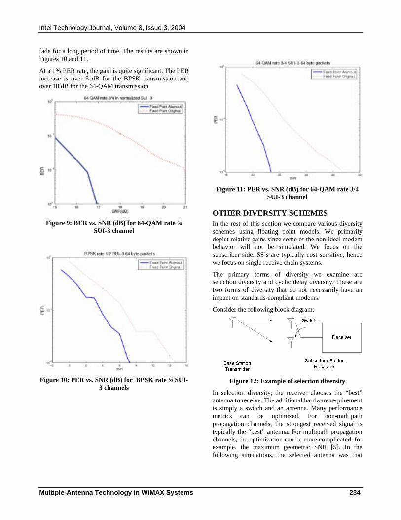
Intel Technology Journal, Volume 8, Issue 3, 2004
Multiple-Antenna Technology in WiMAX Systems 234
fade for a long period of time. The results are shown in Figures 10 and 11.
At a 1% PER rate, the gain is quite significant. The PER increase is over 5 dB for the BPSK transmission and over 10 dB for the 64-QAM transmission.
Figure 9: BER vs. SNR (dB) for 64-QAM rate ¾ SUI-3 channel
Figure 10: PER vs. SNR (dB) for BPSK rate ½ SUI-3 channels
Figure 11: PER vs. SNR (dB) for 64-QAM rate 3/4 SUI-3 channel
OTHER DIVERSITY SCHEMES In the rest of this section we compare various diversity schemes using floating point models. We primarily depict relative gains since some of the non-ideal modem behavior will not be simulated. We focus on the subscriber side. SS’s are typically cost sensitive, hence we focus on single receive chain systems.
The primary forms of diversity we examine are selection diversity and cyclic delay diversity. These are two forms of diversity that do not necessarily have an impact on standards-compliant modems.
Consider the following block diagram:
Figure 12: Example of selection diversity
In selection diversity, the receiver chooses the “best” antenna to receive. The additional hardware requirement is simply a switch and an antenna. Many performance metrics can be optimized. For non-multipath propagation channels, the strongest received signal is typically the “best” antenna. For multipath propagation channels, the optimization can be more complicated, for example, the maximum geometric SNR [5]. In the following simulations, the selected antenna was that
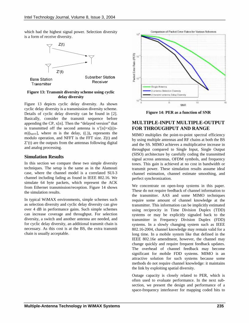
Intel Technology Journal, Volume 8, Issue 3, 2004
Multiple-Antenna Technology in WiMAX Systems 235
which had the highest signal power. Selection diversity is a form of receive diversity.
Figure 13: Transmit diversity scheme using cyclic delay diversity
Figure 13 depicts cyclic delay diversity. As shown cyclic delay diversity is a transmission diversity scheme. Details of cyclic delay diversity can be found in [2]. Basically, consider the transmit sequence before appending the CP, x[n]. Then the “delayed version” that is transmitted off the second antenna is x’[n]=x[((n-m))NFFT], where m is the delay, ((.))a represents the modulo operation, and NFFT is the FFT size. Z(t) and Z’(t) are the outputs from the antennas following digital and analog processing.
Simulation Results In this section we compare these two simple diversity techniques. The setup is the same as in the Alamouti case, where the channel model is a correlated SUI-3 channel including fading as found in IEEE 802.16. We simulate 64 byte packets, which represent the ACK from Ethernet transmission/reception. Figure 14 shows the simulation results.
In typical WiMAX environments, simple schemes such as selection diversity and cyclic delay diversity can give over 4 dB in performance gains. Such simple schemes can increase coverage and throughput. For selection diversity, a switch and another antenna are needed, and for cyclic delay diversity, an additional transmit chain is necessary. As this cost is at the BS, the extra transmit chain is usually acceptable.
Figure 14: PER as a function of SNR
MULTIPLE-INPUT MULTIPLE-OUTPUT FOR THROUGHPUT AND RANGE MIMO multiplies the point-to-point spectral efficiency by using multiple antennas and RF chains at both the BS and the SS. MIMO achieves a multiplicative increase in throughput compared to Single Input, Single Output (SISO) architecture by carefully coding the transmitted signal across antennas, OFDM symbols, and frequency tones. This gain is achieved at no cost in bandwidth or transmit power. These simulation results assume ideal channel estimation, channel estimate smoothing, and perfect synchronization.
We concentrate on open-loop systems in this paper. These do not require feedback of channel information to the transmitter. AAS and some MIMO techniques require some amount of channel knowledge at the transmitter. This information can be implicitly estimated using reciprocity in Time Division Duplex (TDD) systems or may be explicitly signaled back to the transmitter in Frequency Division Duplex (FDD) systems. In a slowly changing system such as IEEE 802.16-2004, channel knowledge may remain valid for a long time. In a mobile system like that defined in the IEEE 802.16e amendment, however, the channel may change quickly and require frequent feedback updates. The overhead of channel feedback may become significant for mobile FDD systems. MIMO is an attractive solution for such systems because some methods do not require channel knowledge: it maintains the link by exploiting spatial diversity.
Outage capacity is closely related to PER, which is often used to evaluate performance. In the next sub-section, we present the design and performance of a space-frequency interleaver for mapping coded bits to

Intel Technology Journal, Volume 8, Issue 3, 2004
Multiple-Antenna Technology in WiMAX Systems 236
tones and antennas. With an optimal receiver, this interleaver can provide M times the spectral efficiency of a 1x1 system at a given range depending on the channel conditions.
Figure 15: System block diagram for space-frequency interleaving
The simplest MIMO receiver is the zero-forcing receiver that inverts the channel, thus recovering M = min(Mt , Mr) transmitted data streams. However, this inversion can cause noise enhancement. A better receiver is the Minimum Mean Squared Error (MMSE) receiver that performs a weighted inverse so as not to magnify noise in the poor channel modes. In general, the optimal receiver that minimizes the probability of error (and achieves capacity) is the Maximum Likelihood (ML) receiver or the Maximum A Posteriori Probability (MAP) receiver. The transmission source may also have a code incorporated. For instance, the OFDMA section of IEEE 802.16-2004 contains transmission matrices for STC that can be used in conjunction with these reception techniques. The performance of some MIMO receivers is outlined in the following sub-sections.
MIMO Transmitter: Space-Frequency Interleaving Space-frequency interleaving is a simple way to provide diversity gain to a spatially multiplexed, coded data stream. This method is not currently standard-compliant. The block diagram for the Space-Frequency Interleaver (SFI) transmitter and receiver is illustrated in Figure 15. Information bits are first encoded by a Forward Error Correction (FEC) encoder, which is a concatenation of Reed-Solomon and convolutional encoders in OFDM-256 IEEE 802.16-2004. After puncturing, the binary coded bits are sent to an SFI, which maps bits to antennas and tones so as to exploit full diversity in both space and frequency. The interleaved bits are then mapped to Gray coded QAM data symbols. The receiver uses the MMSE receiver, and it sends the soft bits into the concatenated convolutional and Reed Solomon decoders.
Details of the interleaver design are available in [12]. We provide a short description here. Let q be the number of bits per QAM symbol, assume 192 data tones (256 point FFT with 64 guard tones+pilots) and M transmit antennas. The interleaver consists of three steps: (1) serial-to-parallel multiplexing of incoming q*192*M bits to M antennas, (2) IEEE 802.16-2004 interleaving on each antenna, and (3) forward circular shift of the bits on each antenna by q*cts, where cts = “cyclic tone shift” is a parameter that must be optimized for each data mode and MIMO configuration.
For example, the IEEE 802.16-2004 interleaver output for BPSK modulation is shown in Figure 16 below:
1 2 3 .. 1 3 5 .. 384 362 364 …
13 14 15 25 27 29 2 4 6
25 26 27 49 51 53 26 28 30
37 38 39 73 75 77 50 52 54
: : :
Figure 16: IEEE 802.16-2004 bit interleaver BPSK, SF interleaver for 2x2 MIMO on antenna 1 and on
antenna 2
In Figure 16 bits are mapped to tones column-by-column. Therefore bits indexed by 1, 13, 25, 37, … are mapped to tones 1, 2, 3, 4, ….etc. Our proposed interleavers are shown in the second two boxes of Figure 16.
Simulation results for this interleaver with BPSK, rate ½, 192 data tones are shown in Figure 17. SUI-3 channel models without spatial correlation are used throughout this section.
Also shown for reference is a simpler interleaver labeled SM, which does not interleave bits across antennas. Instead, it takes contiguous blocks of q*192 bits and maps them to antennas, followed by IEEE 802.16-2004 interleaving on each antenna.
Transmitter
Receiver
Space-frequencyinterleaver
Bits to QAM ,Spatialmapper
802.16dencoder +puncturer
databits
IFFT - CP
IFFT - CP
QAM tosoft bits
Spatialdemapper
(MMSE/MAP)
Deinterleaverdepuncturer
decoder
estimatedbits
FFT - CP
FFT - CP

Intel Technology Journal, Volume 8, Issue 3, 2004
Multiple-Antenna Technology in WiMAX Systems 237
2 3 4 5 6 7 8 9 10 1110
-4
10-3
10-2
10-1
100
SNR (dB)
PE
R (
64 b
yte
pack
ets)
Space-frequency interleaving for 3x3 MIMO (lowest mode)
1x13x3 SM3x3 cts=1
Figure 17: SFI for 3x3 MIMO (lowest mode)
Our interleaver provides gains of 2 to 4 dB over this simple interleaver because it has been designed to extract maximal space-frequency diversity.
At the highest IEEE 802.16-2004 mode with 64-QAM, rate ¾ coding, gains with the interleaver are not as high, but still significant at 1 to 2 dB over SM, as shown in Figure 18.
Figure 18 shows two values of cts: cts=1 and cts=64. Performance of the MMSE receiver is sensitive to the choice of cts, although cts=1 works well for most modes, channel conditions, and MIMO architectures. Performance of the ML receiver is not sensitive to the choice of cts (not shown here).
This suggests that the MMSE receiver induces correlation across space-frequency blocks. The MMSE induces correlation across antennas because of cross-talk, and the channel induces correlation across tones because of limited delay spread. A combination ends up correlating adjacent tones on all antennas. The proposed interleaver places bits on uncorrelated tones and antennas, thereby improving performance with the MMSE receiver.
Figure 18 also shows performance with an SVD receiver, which requires channel feedback to the transmitter in order to diagonalize the channel matrix.
Note in Figures 17 and 18 that the 3x3 architectures fall short of 1x1 by 3 to 5 dB. Therefore these MMSE-MIMO architectures do not maintain range at the higher throughputs.
Advanced receivers are required to improve range at high rates, and they are the subject of the next sub-section.
26 27 28 29 30 31 32 33 34 3510
-2
10-1
100
SNR (dB)
PE
R (
64 b
yte
pack
ets)
Space-frequency interleaving for 3x3 MIMO (highest mode)
1x13x3 SM3x3 cts=13x3 cts=643x3 svd
Figure 18: SFI for 3x3 MIMO at highest mode
MIMO Advanced Receivers: Iterative Decoding A non-iterative receiver similar to that used in the previous sub-section is shown in Figure 19.
SpatialDemapper
QAMto Bit
QAMto Bit
Space-Frequency
De-interleaverUnpuncturer
FECDecoder
( )in1
( )in2
( )ix1
( )ix2
( )ir1
( )ir2
( )is1̂
( )is2ˆ
( )iLb1
( )iLb2
( )id̂ ( )iLb
Figure 19: Illustration of non-iterative receiver
The spatial demapper above decouples the data streams mixed by the channel matrix over the air. The MAP demapper has the best performance and the highest complexity, while linear demappers such as MMSE and ZF have low complexity but poor performance compared to MAP. Recently, techniques such as sphere decoding have been proposed to reduce the complexity of MAP receivers.
After the spatial streams are separated, the “QAM to bit” functional block converts the noisy QAM symbols into Log Likelihood Ratios (LLR) for each punctured, coded bit. For the non-iterative receiver, these LLRs are eventually sent to the FEC decoder and bit decisions are made.
For the iterative receiver, there are many more steps before bit decisions are made. Figure 20 shows an iterative receiver based on the turbo principle [8]. The channel matrix H is treated as a rate one linear block code, which is concatenated with the convolutional and Reed-Solomon codes. Iterations are conducted between the spatial demapper and the FEC decoder by passing extrinsic information (i.e., LLRs) back and forth.
Intel Technology Journal, Volume 8, Issue 3, 2004
Multiple-Antenna Technology in WiMAX Systems 238
MAP SpatialDemapper
Space-Frequency
De-interleaverUnpuncturerBCJR FEC
Decoder
( )in1
( )in2
( )ix1
( )ix2
( )ir1
( )ir2
PuncturerSpace-
FrequencyInterleaver
( )id̂( )iLb
-+
+-
( )ilb
+-
( )ilb1
( )ilb2
Figure 20: Illustration of an iterative receiver
Performance of this iterative receiver is shown in Figure 21 for 2x2 and 2x3 MIMO architectures. All seven rate modes specified in IEEE 802.16-2004 are used to generate this throughput versus SNR curve. For each architecture, all SIMO subsets such as 1x2 and 1x3 are allowed in the set of possible modulations. For each SNR and each channel realization, all possible combinations of data rate and antenna subsets are run to compute throughput and only the maximum throughput is reported. The maximum throughputs of all channel realizations for that SNR are then averaged and the mean throughput is plotted. The number of iterations for 2x2 MAP curve is 4. The SVD curve includes 2x2 with spatial mode puncturing and 1x2 Maximal Ratio Combining (MRC).
We observe the following:
1. 2x2 MAP buys 3-5 dB gain over 2x2 MMSE at higher throughputs.
2. 2x2 SVD buys 2-3 dB over 2x2 MMSE at higher throughputs.
3. 2x3 MMSE buys 5-7 dB over 2x2 MMSE at higher throughputs.
Therefore we buy the most gain by adding an extra receive chain. This hardware cost can be transferred to baseband complexity by using the MAP [9] and BCJR [10] iterative algorithms instead of MMSE, by taking a 1 dB performance hit. The complexity of the MAP
spatial demapper is ( )KMO , where M is the size of the
QAM symbol and K is the number of data streams. This can be rather large for higher order QAMs. We are looking at methods to reduce the complexity of advanced receivers.
-5 0 5 10 15 20 25 300
5
10
15
20
25
SNR = Es/N0 (dB)
Thr
ough
put
(Mbp
s)
802.16d, 1x1, 2x2, 2x3, SUI 3
1x12x2 and 1x2, MMSE2x2 and 1x2, MAP2x2 and 1x2, SVD2x3 and 1x3, MMSE
Figure 21: Advanced receivers for 2x2 and 2x3
CONCLUSION We have shown that multiple-antenna techniques can greatly enhance the performance of wireless transmission systems. Systems are currently trending towards using multiple antennas at the BS and future systems may evolve to multiple antenna systems at the SS. We have demonstrated that Alamouti reception, circular delay diversity, and selection diversity are simple schemes that can increase performance greatly. More advanced MIMO techniques can increase performance well beyond the current limits of data rate and reach.
ACKNOWLEDGEMENTS The authors thank Hakim Mesiwala, Wendy Wong, Sigang Qiu, Tony Liu, and Bo Xia for simulation and channel modeling support.
REFERENCES [1] H. Heiskala and J. Terry, “OFDM Wireless LANs: A
Theoretical and Practical Guide,” SAMS, 2002.
[2] S. Alamouti, “A Simple Transmit Diversity Technique for Wireless Communications,” IEEE Journal on Select Areas in Communications, Vol. 16, No. 8, pp. 1451-1458, October 1998.
[3] R. Monzingo and T. Miller, Introduction to Adaptive Arrays, Scitech Publishing, Raleigh, NC, 2004.
[4] M. Simon, S. Hinedi, and W. Lindsey, Digital Communication Techniques Signal Design and Detection, Prentice Hall, Englewood Cliffs, NJ, 1995.
[5] J. Cioffi, “Course Reader for EE379A,” Stanford University, 2002.
Intel Technology Journal, Volume 8, Issue 3, 2004
Multiple-Antenna Technology in WiMAX Systems 239
[6] G. J. Foschini, et al., “On Limits of Wireless Communications in a Fading Environment Using Multiple Antennas,” Wireless Personal Communications, vol. 6, no. 3, pp. 311-335, March 1998.
[7] G. G. Raleigh and J. M. Cioffi, “Spatio-temporal Coding for Wireless Systems,” IEEE Trans. Communication, Vol. 4, No. 3, pp. 357-366, 1996.
[8] J. Hagenauer, “The turbo principle–tutorial introduction and state of the art,” in Proceedings International Symposium on Turbo Codes & Related Topics, Brest, France, pp. 1-11, Sept. 1997.
[9] J. G. Proakis, Digital Communications, McGraw Hill, 4th Ed., Aug. 2000.
[10] L. R. Bahl, et al., “Optimal decoding of linear codes for minimizing symbol error rate,” IEEE Transactions on Information Theory, pp. 284–287, March 1974.
[11] I. E. Telatar, “Capacity of multi-antenna Gaussian channels,” AT&T Bell Labs Tech. Memo., 1995.
[12] “Space-frequency interleaving for MIMO-OFDM,” in IEEE TG802.11n, S. Sandhu, December 2003.
[13] E. Larsson and Petre Stoica, Space Time Block Coding for Wireless Communications, Cambridge University Press, Cambridge, UK, 2003.
[14] A. Paulraj, R. Nabar, and D. Gore, Introduction to Space-Time Wireless Communications, Cambridge University Press, Cambridge, UK, May 2003.
AUTHORS’ BIOGRAPHIES Atul Salvekar is a member of the technical staff for the Broadband Products Group. His last assignment was designing algorithms for the IEEE 802.16-2004 modem. Atul’s primary interest is in signal processing and communications. He is also an avid tennis player and loves playing the piano. Atul received his B.S. degree in Electrical Engineering from Caltech and his M.S. and Ph.D. degrees in Electrical Engineering from Stanford University in 1996, 1998, and 2002, respectively. He also has an M.S. degree in statistics from Stanford University. His e-mail is atul.a.salvekar at intel.com.
Sumeet Sandhu is a senior staff researcher in the Corporate Technology Group in Santa Clara. As CTG MIMO lead for the 802.11n standards effort, she developed a number of algorithms and IP which are part of the Intel 802.11n proposal. Her primary interests are space-time coding, signal processing, and FEC for point-to-point wireless systems and distributed
processing for cognitive networks. Prior to Intel, she has held positions at Iospan Wireless, Hughes Research Laboratories, and Bell Laboratories. She holds a Ph.D. from Stanford University and a B.S and M.S from MIT. Her e-mail is sumeet.sandhu at intel.com.
Qinghua Li is a researcher in Intel’s Corporate Technology Group. He is currently developing high throughput techniques for Intel’s WLAN products and IEEE 802.11n standard. Before he joined Intel in 2001, he worked for Ericsson and Nokia for short periods. His research lies in the hot areas of wireless communications including MIMO, SDMA, UWB, MAC, indoor wireless channel modelling, CDMA, FEC coding, multiuser detection, and interference mitigation. He received B.E., M.E., and Ph.D. degrees from South China University of Technology, Tsinghua University, and Texas A&M University, respectively in 1992, 1995, and 2001, all in Electrical Engineering. His e-mail is qinghua.li at intel.com.
Minh-Anh Vuong is a senior engineer in the Broadband Wireless Division. He is working on multiple projects. He has worked on algorithms, firmware, and system modelling. Minh-Anh received his B.S. degree in Electrical Engineering from Grenoble, France and his M.S. degree in Electrical Engineering from Arizona State University. His e-mail is minh-anh.q.vuong at intel.com.
Xiaoshu Qian currently manages the system group in the Broadband Wireless Division at Intel Corporation to help develop the next-generation broadband wireless communication chips. In the past, he has worked primarily in the areas of algorithm development, DSP architecture, and logic design for multimedia and communication chips. He received a Ph.D. degree in Electrical Engineering, an M.S. degree in Computer Science, and an M.S. degree in Mathematics, all from the University of Rhode Island. He also holds a B.S. degree in Physics from Zhejiang University in China. His e-mail is xiaoshu.qian at intel.com.
Copyright © Intel Corporation 2004. This publication was downloaded from http://developer.intel.com/.
Legal notices at http://www.intel.com/sites/corporate/tradmarx.htm.

Intel Technology Journal, Volume 8, Issue 3, 2004
Multiple-Antenna Technology in WiMAX Systems 240
THIS PAGE INTENTIONALLY LEFT BLANK

Fully Integrated CMOS Radios from RF to Millimeter Wave Frequencies 241
Fully Integrated CMOS Radios from RF to Millimeter Wave Frequencies
Luiz M. Franca-Neto, Intel Communications Group, Intel Corporation Roger Eline, Intel Communications Group, Intel Corporation
Bisla Balvinder, Intel Communications Group, Intel Corporation
Index words: 802.16, RF CMOS, microwave, millimeter wave, deep nwell, mixed-signal, RFIC, analog IC, flip-chip package, passives on the package, System-on-a-Chip (SoC), System-on-a-Package (SoP), backing-off method, optimum-pump method, 60 GHz, 100 GHz circuits, Wi-Fi, WiMAX.
ABSTRACT
This paper reviews (a) recent CMOS demonstrations of capabilities for Radio Frequency (RF), microwave, and millimeter wave circuits from 1 GHz to 100 GHz, (b) advances in on-die isolation structures for integrating radio’s delicate circuits with very noisy general-purpose processors on the same die, and (c) entirely novel design methods for complex RF passive networks on the package substrate by engineering the physical design of the package substrate (no discrete passive components added to the package) that diminish the silicon area requirements for multiband multiprotocol CMOS radios and frees silicon area to host complex digital processing and communication engines. Circuit design techniques are discussed to cope with intrinsic CMOS challenges and technology scaling. Building upon these developments, a vision for CMOS technology and platform direction is proposed.
INTRODUCTION From 1995 to 2004, CMOS technology has proven its Radio-Frequency (RF), microwave, and millimeter wave capabilities by demonstrations of fully integrated key circuit blocks from 1 GHz to 100 GHz [1-7]. Low Noise Amplifiers (LNAs) with noise figures as low as previously reported for compound semiconductor technology started to be reported for fully integrated CMOS realizations. The intrinsic higher 1/f (flicker) noise corner in CMOS technology compared to bipolar technologies found compensation in novel circuit-level methods.
CMOS scaling enabled the technology to reach for higher GHz frequencies, and the higher speeds offer other
opportunities to compensate at the circuit level for intrinsic technology drawbacks.
Only one intrinsic technology problem appeared to be fundamentally unsuited for technology scaling: RF transmission power levels. As CMOS scales, lower voltages are tolerated at the transistor terminals. Circuit-level solutions using power-combining techniques to add the power of parallel Power Amplifiers (PAs) in CMOS have met with success. Power combination of parallel PAs have being used on die [8], and in this paper, we discuss novel power-combining circuits on the package. These power-combining circuits on the package become en passant the supporting structure for MIMO or general antenna-diversity/beam-forming-based radios. This last step means the circuits on the package support what can be recognized as power combining on air to cope with CMOS RF power transmission limitations.
Nevertheless, CMOS technology’s full potential would not be realized if only standalone radios are fabricated. Integration of delicate radio and general-purpose processors is the next goal. The co-habitation of delicate RF circuits and a very noisy general-purpose processor such as a 1 GHz 55 W Pentium® 4 processor on the same die was shown to be possible by proper circuit techniques, special deep nwell isolation structures, and exploitation of the digital substrate noise spectrum structure [9]. Novel entire designs of complex RF passive networks realized by trace engineering (no
® Pentium is a registered trademark of Intel Corporation or its subsidiaries in the United States and other countries.

Intel Technology Journal, Volume 8, Issue 3, 2004
Fully Integrated CMOS Radios from RF to Millimeter Wave Frequencies 242
discrete components added) on the package substrate diminished the silicon area required for multiband multiprotocol radios and freed silicon area for hosting more digital circuits, processing units, and communications system new features [10].
Building on these developments, at the platform level, considering the PC motherboard, we articulate a vision for a new CMOS computing and communication platform. Instead of trying to integrate multiband multiprotocol radio circuits into already densely packed chips like a Pentium processor and its companion chipsets, it might be more promising to re-think the PC motherboard as a multiprocessor platform, where the processor and chipset will make a new ecosystem with two new chips that provide for multiband multiprotocol radios. In other words, a platform which is capable of supporting the variety of current standards and is also able to support always evolving standards is proposed. This new platform can extend its reach to encompass in a modular fashion wireless communications from 700 MHz, over the newly vacant TV bands, all the way to 60 GHz, where 7 GHz of bandwidth enables indoor high data rate omnidirectional wireless links and outdoor line-of-sight (LOS) high data rate backbone links.
The next sections in this paper detail the CMOS technology scaling effects on its RF, microwave, and millimeter wave capabilities; the new developments in package technology and novel CMOS-compatible devices; and further elaborate on the opportunities in the area of platforms for CMOS.
CMOS (EXCESS) THERMAL NOISE. In the radio receiver front-end, the Low Noise Amplifier (LNA) is the first key component in which CMOS technology needed to prove its adequacy. By the aggressive scaling of CMOS technology, there was always the concern that the high field transport in the channel could produce too large a carrier velocity dispersion, and therefore microwave noise, significantly above thermal noise. That’s because apart from not always having consistent definitions in the literature for excess thermal noise, a conductor or semiconductor is only guaranteed to develop thermal noise levels in thermal equilibrium, and will tend to develop noise levels above this equilibrium level whenever a dc current flows through them and more so as the electric field applied to the transport increases [11, 12]. The concern was that the noise level could become progressively higher with scaling in such a way that the gain of the device could not compensate and, in this case, scaling would start to produce higher noise figure transistors at some point.
Fortunately, the opposite has happened so far and even though the product gmRo decreases with nanometer scaling, the device transconductance (gm), with typical RF device loading, still provides higher gain with CMOS scaling to compensate for the additional noise in the channel high field transport. Moreover, carrier transport in the channel of 90 nm CMOS and future nodes may experience a qualitative change in properties that leads to less carrier velocity dispersion due to a diminishment in the likelihood of carrier scattering events in such extremely short channels. If this becomes a new trend it will progressively benefit CMOS technology and will offer unprecedented lower noise figures with scaling at frequencies above 10 GHz. Currently, minimum noise figure (NFmin) numbers for CMOS transistors in 0.18 µm and 90 nm are respectively 1 dB and 0.5 dB at 5.5 GHz. These are at par with the best numbers offered by SiGe and other compound semiconductor technologies at these frequencies.
In reality, CMOS transistors are becoming virtually “noiseless” for practical purposes below 10 GHz. That completely shifted the design and optimization procedures for LNAs to include noise contribution from passives. A circuit-level method was developed by one of the authors to globally optimize the noise figure of LNAs, taking into account noise contributions from both passive and active devices. It became an extension of S-parameter methods used in traditional microwave methods and was named the “backing-off” method [6].

Intel Technology Journal, Volume 8, Issue 3, 2004
Fully Integrated CMOS Radios from RF to Millimeter Wave Frequencies 243
Figure 1: Backing off from active device’s NFmin: length of impedance transformer’s transmission line is shortened to diminish the noise contributions from lossy passives at the expense of a small increase in the
contribution from the active devices, but still producing a lower noise figure for the final LNA
Traditional microwave design approaches assume high-quality passives. Thus, low noise amplifier designs primarily seek the transistor’s NFmin and implement its optimum source (driving) impedance, so far as this does not compromise unacceptably the gain of the amplifier or its input match [13]. In contrast, when passives are implemented on a CMOS die, because of geometric constraints (more on geometric implications for on-die realizations later), their low Q makes such an approach sub-optimal. In effect, low noise amplifiers are optimally designed if backing off from the active device’s NFmin is used. This new approach minimizes the final noise figure of the LNA by trading off a small increase in transistor noise for a much lower noise contribution from the lossy passives.
Figure 1 illustrates how the backing-off approach is applied to the definition of transmission line length of the impedance transformer (Trans1) in the Input Matching Network (IMN) of the amplifier. Constant gain circles (15 dB and 10 dB gain, Zload referred) and constant noise figure circles (Zin
* referred) for a cascode structure with inductive source degeneracy is depicted. Note that if the design of the input matching network was done with high-quality passives the length of the impedance transformer
would have been as close to L1+L2 (note “L” stands for length rather then inductance in this discussion) as an acceptable input mismatch would allow. However, once low-Q passives are used, making the length of Trans1 be shortened to L1, despite an increase in the cascode structure’s noise, leads to smaller noise figures for the final LNA. Moreover, the pair Zload and Zin* for 10 dB gain, identified in Figure 1, stresses that backing off can lead not only to a lower noise figure but can also lead to minimal mismatch at the input port of the amplifier. In general, the amount of back off is a function of how low the Q of the passives is and how slowly the active devices’ noise figure changes as their driving source move away from their optimum (i.e., how small the active device’s noise parameter Rn is). The disposition of constant gain circles, constant noise circles, and stability circles in the Smith-chart will change with transistor size, amount of source inductive degeneracy, and frequency of operation of the LNA. In the designs presented in this paper, for every step in the optimization process, backing off is always checked around every design point iteration.
Figure 2: Schematic and corresponding layout for a 17 GHz LNA in 0.18 µm CMOS
Even though the procedure was illustrated for 17 GHz and 24 GHz LNAs, and on-die microstrip segments were used for the passives, the method is readily applicable to both lower and higher frequencies, with the only visual effect of using lumped passive components (spiral inductors) at lower GHz frequencies and distributed passive components (microstrips) at higher frequencies.
Figure 2 shows the simplified schematics and the corresponding layout for a 17 GHz LNA in 0.18 µm CMOS.
Figure 3 shows die photos of both 17 GHz and 24 GHz LNAs in 0.18 µm. These designs weren’t the most compact designs possible since they also aimed at proving abrupt curves make for only minimal affect in microstrip performance on-die, and that on-die
0 1.0
1.0
-1.0
10.010.0
-10.0
5.0
5.0
-5.0
2.0
2.0
-2.0
3.0
3.0
-3.0
4.0
4.0
-4.0
0.2
0.2
-0.2
0.4
0.4
-0.4
0.6
0.6
-0.6
0.8
0.8
-0.8
17GHz
15dB10dB
4.2dB (NF)
5.2dB (NF)
Back-off
Total lengthof ImpedanceTransformer L1
L2
25pHMC1
Trans1
RFin+L1 L2
Zload(10dB gain)
Z*in(for 10dB gain)
ZloadZin*
Zin
0 1.0
1.0
-1.0
10.010.0
-10.0
5.0
5.0
-5.0
2.0
2.0
-2.0
3.0
3.0
-3.0
4.0
4.0
-4.0
0.2
0.2
-0.2
0.4
0.4
-0.4
0.6
0.6
-0.6
0.8
0.8
-0.8
17GHz
15dB10dB
4.2dB (NF)
5.2dB (NF)
Back-off
Total lengthof ImpedanceTransformer L1
L2
0 1.0
1.0
-1.0
10.010.0
-10.0
5.0
5.0
-5.0
2.0
2.0
-2.0
3.0
3.0
-3.0
4.0
4.0
-4.0
0.2
0.2
-0.2
0.4
0.4
-0.4
0.6
0.6
-0.6
0.8
0.8
-0.8
17GHz
15dB10dB
4.2dB (NF)
5.2dB (NF)
Back-off
Total lengthof ImpedanceTransformer L1
L2
25pHMC1
Trans1
RFin+L1 L2
Zload(10dB gain)
Z*in(for 10dB gain)
ZloadZin*
Zin
RFin +
RFin -
RFin +
RFout +
M1
M2
Le
bias2
Lload1
M3
M4
MC1
Lload2
Trans2
Trans1
MC2
bias4
Mstb
bias3
AGCMpAGC
Towards other halfof differential circuit
RFout +
Rfout -
Virtual-ground axis (differential operation)
metal1
metal6
Microstrip-on-die
Metal 1 ground-plane
h
RFin +
RFin -
RFin +
RFout +
M1
M2
Le
bias2
Lload1
M3
M4
MC1
Lload2
Trans2
Trans1
MC2
bias4
Mstb
bias3
AGCMpAGC
Towards other halfof differential circuit
RFout +
Rfout -
Virtual-ground axis (differential operation)
metal1
metal6
Microstrip-on-die
Metal 1 ground-plane
h
Intel Technology Journal, Volume 8, Issue 3, 2004
Fully Integrated CMOS Radios from RF to Millimeter Wave Frequencies 244
transmission lines can be used for robust design of inductance as small as 25 pH. These 17 GHz and 24 GHz LNAs delivered final noise figures below 6 dB (world record in 0.18 µm). LNA designs at 2.4 GHz and 5.2 GHz using backing-off method delivered under 3 dB noise figures even with input matching network realized on-die, also a world record for 0.18 µm. These results qualify CMOS for 802.16 applications with a healthy margin. [14].
Figure 3: Die photos of 17 GHz and 24 GHz LNAs in 0.18 µm CMOS. Noise figures below 6 dB (world
record) at these frequencies include input matching network (IMN) on die. At 2.4 GHz and 5.2 GHz noise figures are below 3 dB, IMN included, for the same
CMOS technology.
Both 17 GHz and 24 GHz LNA designs were successful at first trial. They were designed using S-parameter measurements from laid out CMOS transistors on wafer. No CMOS modeling was used, and device sizing was still retained as a designer’s degree of freedom. Larger or smaller devices could have their S-parameter calculated on the computer straightforwardly since larger devices are just smaller ones in parallel. All the microstrips on the die were electromagnetic field solved, and their S-parameter behavior was determined as well. Again, no modeling of these passives to their constitutive components was necessary. All this indicates CMOS RF and microwave designs will benefit from seamlessly merging methods and techniques from both VLSI and microwave domains, and this is discussed later in this paper.
CMOS 1/F (FLICKER) NOISE Due to the very nature of carrier transport in CMOS transistors taking place at the interface between SiO2 and Si, the 1/f corner frequency in CMOS transistors is much higher than the corner frequency for bipolar transistors.
At the intrinsic device level, therefore, CMOS suffers from a physically-based drawback. And, the introduction of new high-κ dielectric material in the gate of future CMOS technology nodes will tend to increase the 1/f noise levels of CMOS transistors.
RF CMOS designers have worked successfully through mitigation procedures. First, whenever fast enough, PMOS transistors are used instead of NMOS transistors as the device for oscillators and Voltage Controlled Oscillators (VCOs). It was already noted that the CMOS drawback of typically 10 dB in 1/f noise in comparison to bipolar devices could be compensated for by (a not always desirable) 4X increase in power dissipation in the final oscillator and VCO designs in CMOS. That stemmed from the experiment of paralleling four identical coupled oscillators to produce a single oscillator signal. Since the individual oscillators’ signals add in amplitude, and the uncorrelated noise from the identical oscillators add in power, paralleling oscillators yield lower phase noise oscillations for the final assembly [15].
More importantly however, new understanding of the manifestation of the upconversion of 1/f noise as close in phase-noise in oscillators and VCOs opened the perspective of more sophisticated circuit-level approaches to low noise oscillators and VCO designs in CMOS [16-22]. First of all, contrary to the assumption of many designers, an assumption encouraged by Leeson’s formula [15, 22], the 1/f corner frequency of the CMOS transistors will not be the first corner frequency of the oscillator phase noise spectrum [18-20]. Actually, experimental results have frequently indicated the incorrectness of this assumption [22]. In reality, circuit-level considerations of topological and current drive symmetry can push the oscillator phase noise first corner to within kHz frequencies from the carrier’s frequency, thus yielding very low noise oscillations, even in CMOS technology where the 1/f corner can be in the hundreds of MHz frequencies. This new appreciation of phase noise readily led to a demonstration of unprecedented low-phase noise oscillators and VCO designs in CMOS, without the need to increase unduly the power consumption.
On top of that, VCOs are used in PLL- or DLL-based synthesizers in radio designs. This allows for another level of circuit design techniques to be used for further diminishing phase noise. The idea is to make the loop force the internal VCO to follow the much lower-phase
LNA 17GHz die photo
LNA 24GHz die photo
LNA 17GHz die photoLNA 17GHz die photo
LNA 24GHz die photoLNA 24GHz die photo
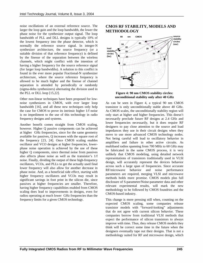
Intel Technology Journal, Volume 8, Issue 3, 2004
Fully Integrated CMOS Radios from RF to Millimeter Wave Frequencies 245
noise oscillations of an external reference source. The larger the loop gain and the loop bandwidth, the lower the phase noise for the synthesizer output signal. The loop bandwidth of PLL and DLL designs is typically 10% of the lowest frequency into the phase detector, which is normally the reference source signal. In integer-N synthesizer architecture, the source frequency (or a suitable division of that reference frequency) is defined by the finesse of the separation between the wireless channels, which might conflict with the intention of having a higher frequency for the source reference signal (for larger loop bandwidths). A solution to this conflict is found in the ever more popular Fractional-N synthesizer architecture, where the source reference frequency is allowed to be much higher and the finesse of channel separation is attended by periodically or randomly (sigma-delta synthesizers) alternating the division used in the PLL or DLL loop [15,22].
Other non-linear techniques have been proposed for low-noise synthesizers in CMOS, with ever larger loop bandwidth [16], and all these new techniques only help the case for CMOS to prove its intrinsic higher 1/f noise is no impediment to the use of this technology in radio frequency designs and systems.
Another benefit comes straight from CMOS scaling, however. Higher Q passive components can be achieved at higher GHz frequencies, since for the same geometry available for passives, Q increases with the square root of the frequency [23, 24]. Once CMOS scaling enables oscillator and VCO designs at higher frequencies, lower-phase noise operation is achieved by the use of these higher Q components, since thermal noise from passives also affects phase noise as well as the transistor’s 1/f noise. Finally, dividing the output of these high-frequency oscillators, VCOs, and PLLs to get the actually used final lower frequency will also allow for another decrease in phase noise. And, as a beneficial side effect, starting with higher frequency oscillators and VCOs may result in significant savings in foot print in the silicon die, since passives at higher frequencies are smaller. Therefore, having higher frequency capabilities enabled from CMOS scaling does lead to improvements in designs, even for radios operating at much lower GHz frequencies than the frequency limits for a given CMOS technology.
CMOS RF STABILITY, MODELS AND METHODOLOGY
Figure 4: 90 nm CMOS stability circles: unconditional stability only after 40 GHz
As can be seen in Figure 4, a typical 90 nm CMOS transistor is only unconditionally stable above 40 GHz. As CMOS scales, the unconditionally stability region will only start at higher and higher frequencies. This doesn’t necessarily preclude future RF designs at 2.4 GHz and lower frequencies necessarily, but it does require RF designers to pay close attention to the source and load impedances they use in their circuit designs when they move to use more advanced CMOS technology nodes. Not being careful will lead to oscillatory behavior in amplifiers and failure in other active circuits. As multiband radios spanning from 700 MHz to 60 GHz may be fabricated in the same CMOS process, it is very unlikely that CMOS modeling, using detailed network representations of transistors traditionally used in VLSI design, will accurately represent the devices behavior across such a large span of frequencies. Since accurate RF/microwave behavior and noise performance parameters are required, merging VLSI and microwave methods holds more promise. CMOS models plus full disclosure of S-parameter/Noise-parameter data and other relevant experimental results, will mark the new methodology to be followed by CMOS foundries and the CMOS-based industry.
This change is more pressing still when, counting on the expected CMOS scaling, some companies release transistor models with “forward-looking” adjustments that do not agree with current silicon behavior. These companies borrow from traditional VLSI methods that expect the performance of silicon transistors to always improve with time. Thus, they release CMOS models they think will be correct some time in the future when the designers eventually tape out their designs. That is not a methodology suited for RF and microwave design, which
01.0
1.0
-1.
10.0
10.0
-10.0
5.0
5.0
-5.0
2.0
2.0
-2.
3.0
3.0
-3.0
4.0
4.0
-4.0
0.2
0.2
-0.2
0.4
0.4
-0.4
0.6
0.6
-0.
0.8
0.8
-0.
M1
port 1
port 2
90 nm CMOS
load stability circles (lsc)
source stability circles (ssc)
10
20
30
40 50
10
20
30
40
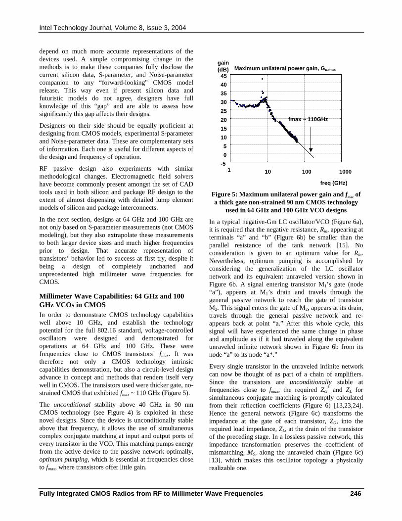
Intel Technology Journal, Volume 8, Issue 3, 2004
Fully Integrated CMOS Radios from RF to Millimeter Wave Frequencies 246
depend on much more accurate representations of the devices used. A simple compromising change in the methods is to make these companies fully disclose the current silicon data, S-parameter, and Noise-parameter companion to any “forward-looking” CMOS model release. This way even if present silicon data and futuristic models do not agree, designers have full knowledge of this “gap” and are able to assess how significantly this gap affects their designs.
Designers on their side should be equally proficient at designing from CMOS models, experimental S-parameter and Noise-parameter data. These are complementary sets of information. Each one is useful for different aspects of the design and frequency of operation.
RF passive design also experiments with similar methodological changes. Electromagnetic field solvers have become commonly present amongst the set of CAD tools used in both silicon and package RF design to the extent of almost dispensing with detailed lump element models of silicon and package interconnects.
In the next section, designs at 64 GHz and 100 GHz are not only based on S-parameter measurements (not CMOS modeling), but they also extrapolate these measurements to both larger device sizes and much higher frequencies prior to design. That accurate representation of transistors’ behavior led to success at first try, despite it being a design of completely uncharted and unprecedented high millimeter wave frequencies for CMOS.
Millimeter Wave Capabilities: 64 GHz and 100 GHz VCOs in CMOS In order to demonstrate CMOS technology capabilities well above 10 GHz, and establish the technology potential for the full 802.16 standard, voltage-controlled oscillators were designed and demonstrated for operations at 64 GHz and 100 GHz. These were frequencies close to CMOS transistors’ fmax. It was therefore not only a CMOS technology intrinsic capabilities demonstration, but also a circuit-level design advance in concept and methods that renders itself very well in CMOS. The transistors used were thicker gate, no-strained CMOS that exhibited fmax ~ 110 GHz (Figure 5).
The unconditional stability above 40 GHz in 90 nm CMOS technology (see Figure 4) is exploited in these novel designs. Since the device is unconditionally stable above that frequency, it allows the use of simultaneous complex conjugate matching at input and output ports of every transistor in the VCO. This matching pumps energy from the active device to the passive network optimally, optimum pumping, which is essential at frequencies close to fmax, where transistors offer little gain.
Figure 5: Maximum unilateral power gain and fmax of a thick gate non-strained 90 nm CMOS technology
used in 64 GHz and 100 GHz VCO designs
In a typical negative-Gm LC oscillator/VCO (Figure 6a), it is required that the negative resistance, Rin, appearing at terminals “a” and “b” (Figure 6b) be smaller than the parallel resistance of the tank network [15]. No consideration is given to an optimum value for Rin. Nevertheless, optimum pumping is accomplished by considering the generalization of the LC oscillator network and its equivalent unraveled version shown in Figure 6b. A signal entering transistor M1’s gate (node “a”), appears at M1’s drain and travels through the general passive network to reach the gate of transistor M2. This signal enters the gate of M2, appears at its drain, travels through the general passive network and re-appears back at point “a.” After this whole cycle, this signal will have experienced the same change in phase and amplitude as if it had traveled along the equivalent unraveled infinite network shown in Figure 6b from its node “a” to its node “a*.”
Every single transistor in the unraveled infinite network can now be thought of as part of a chain of amplifiers. Since the transistors are unconditionally stable at frequencies close to fmax, the required ZG
* and ZL for simultaneous conjugate matching is promptly calculated from their reflection coefficients (Figure 6) [13,23,24]. Hence the general network (Figure 6c) transforms the impedance at the gate of each transistor, ZG, into the required load impedance, ZL, at the drain of the transistor of the preceding stage. In a lossless passive network, this impedance transformation preserves the coefficient of mismatching, MS, along the unraveled chain (Figure 6c) [13], which makes this oscillator topology a physically realizable one.
1 10 100 1000 -5
0
5
10
15
20
25
30
35
40
45 Maximum unilateral power gain, Gu,max
gain (dB)
freq (GHz)
fmax ~ 110GHz

Intel Technology Journal, Volume 8, Issue 3, 2004
Fully Integrated CMOS Radios from RF to Millimeter Wave Frequencies 247
(a)
(b)
(c)
Figure 6: From negative-gm to optimum pumping
Depending on the transistor technology, the number of stages required for a multiple-of-360o phase shift in the signal may be awkwardly high. Figure 7 shows how delay lines are added in one of the three possible general cases for the optimum pair Γs and ΓL [7]. The impedance transformation along these distributed networks crosses the horizontal-axis (real impedance axis) of the Smith-chart along one of its transmission lines. At this cross, a lossless transmission line segment of characteristic impedance defined by the point of cross can be added to the VCO’s passive network without disturbing the optimum-pumping impedance transformation. The length (delay) added depends on the number of stages desired for the final VCO. It is important to note the optimum-pumping method exploits the unconditional stability of the transistor whereas the standard microwave approach exploits the device instability for oscillator design [13,23,24].
Figure 7: Strategic delay element introduction: “L1” and “L2” are lengths of transmission lines
In this work, no commercial CMOS model was used. 90 nm logic CMOS transistors were laid out and characterized by S-parameter measurements up to 50 GHz. The transistor S-parameters were extrapolated to 64 GHz and 100 GHz. The distributed passive networks were realized using microstrip-on-die, with ground plane in metal-1 and traces in metal-7 layers. These passive networks were Electromagnetic Field solved using a commercial program [25]. Ground plane in metal-1 isolated the passive networks from silicon substrate losses.
Figure 8 shows the photo die with a description of the components of both 64 GHz and 100 GHz VCOs. Signals were taped from the VCO’s core at its lowest impedance (lowest swing) with a high-impedance tap for minimum disturbance of oscillations.
Figure 8: 64 GHz and 100 GHz VCOs: single-transistor core die photo
The ¼-wavelength-transmission-line tap from the VCO core to the transistor buffer further diminished the signal to be measured. The pads are part of the output network of the buffer; microstrip stubs were added to properly
impedance converter
… …
MS MS MS MS MS
impedance converter
a to a* needs gain>1 and integer number of 360o phase shift
node “ a ”
general net
…
node “ a* ”
general net general net …
M1 M2 a a a*
Rin = -2/gm
L1 L2
C1 C2
a b
64 GHz VCO 100 GHz VCO
VCO ¼ λ t.lines
delay
VCCVctrl VctrlGND
GND GND GND OUT OUTGND GND
VCCVctrl Vctrl
L1
L2
ZLOAD
L1
OUT
L2
Z
Z LOAD
DELAY
Z*
Z* LOAD
buffer
delay at the cross of real axis
Z GATE
Case1: |ΓG| = |ΓL|
Γ G
Γ L
¼ λ t.lines
bias & tap
ΓS ΓL Γ*L Γ*S ΓS ΓL

Intel Technology Journal, Volume 8, Issue 3, 2004
Fully Integrated CMOS Radios from RF to Millimeter Wave Frequencies 248
tune the pad impedance to maximum buffer gain (Figure 8).
Figure 9: 100 GHz VCO: 4-transistor-core die photo
The 64 GHz and 100 GHz VCO signals were measured to be centered at 63.6 GHz and 103.9 GHz. This was calculated by simulating that the measured signal for both 64 GHz and 100 GHz meant a 0.4 Vp-p swing at the VCOs’ cores at their largest swing point. Both VCOs used a 1.0 V power supply and drew 20 mA (64 GHz) and 30 mA (100 GHz) of current. Both VCOs were completely functional from -50oC to 110oC. Center frequency changed approximately 5 GHz (100 GHz) and 3 GHz (64 GHz) in this temperature range, because of the relatively small temperature dependence of the phase shift contribution from the passive network in the VCO core. Consistently, the gains for both VCOs were in the range of 2 GHz/V, either through body bias or supply voltage control. These were successful designs at first try that firmly established CMOS capabilities well into millimeter wave frequencies.
Figure 9 shows a 100 GHz 4-transistor core oscillator that was designed by adjusting the delay elements. In this topology quadracture output signals are produced.
RF AND DIGITAL PROCESSOR IN THE SAME DIE Once CMOS technology capabilities for RF applications is established even to extreme 100 GHz frequencies, the next step is to go beyond standalone radio design. Communications and computing have synergies that can be exploited in RF and digital processor integrations in the same die.
In order to demonstrate that such an integration is possible even in the extreme case of a very noisy digital processor with clock frequencies in the GHz range and
delicate RF circuits typically sensitive to at least -76 dBm signals from the antenna, we started by measuring how noisy the substrate of a Pentium 4 is.
Figure 10: Redundant logic delay chains: unused transistors engineered into noise sensors
Intel processors are taped out with extra logic delay chains for pre-product investigations (Figure 10). These extra transistors are left in the commercial microprocessors without doing any work. These redundant transistors were engineered as substrate noise sensors by Focused Ion Beam (FIB) work from the back of the die. These transistors were unconnected from the rest of the microprocessor circuits and their terminals were brought externally onto the back of the wafer (Figure 11). Substrate activity (noise), which modulates the body bias of these transistors, is displayed by the spectrum analyzer (Figure 12). Figure 11 shows the layout as seen from the back of the die, and it shows the vias and wires for connecting the source, drain, and gate of a test transistor. 1.2 mVrms noise measured at the drain of a 5 µm-wide noise sensor located at the center of the die translates (by the noise sensor transfer function) to 100 mVrms noise on the substrate. These measurements corresponded to 15 W power dissipation produced by the excitation of the 1 GHz clock grid as can be seen by the noise spectrum developed. Assuming substrate noise power is directly related to the microprocessor (dynamic) power dissipation [26], the same microprocessor dissipates 55 W and thus produces 190 mVrms substrate noise at full operation. Because of a typical activity of 10% (for the logic gates), this additional substrate noise on an actual application of this microprocessor, is concentrated from dc to 150 MHz.
The fundamental insight guiding this research is that high-performance microprocessors, with clocks at GHz frequencies, develop substrate noise with a spectrum structure that can be exploited to place RF narrow-band signals in valleys of low-substrate noise levels in the frequency spectrum. This can be achieved by placing and retrieving feeble bandwidth-limited RF information
VCO’s core
delay
100 GHz VCO
core transistors
VCC
¼ λ t.lines
Quadracture outputs (I & Q)
a b
µProcessor
BLOCK 1 BLOCK 2
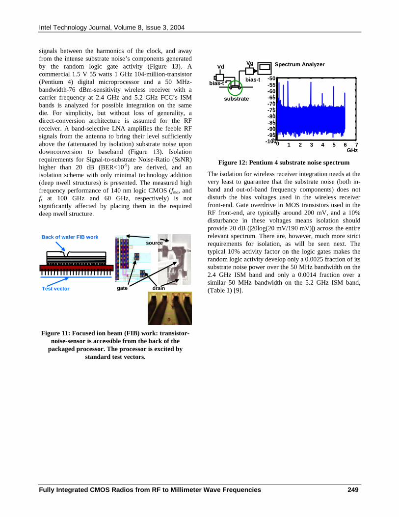
Intel Technology Journal, Volume 8, Issue 3, 2004
Fully Integrated CMOS Radios from RF to Millimeter Wave Frequencies 249
signals between the harmonics of the clock, and away from the intense substrate noise’s components generated by the random logic gate activity (Figure 13). A commercial 1.5 V 55 watts 1 GHz 104-million-transistor (Pentium 4) digital microprocessor and a 50 MHz-bandwidth-76 dBm-sensitivity wireless receiver with a carrier frequency at 2.4 GHz and 5.2 GHz FCC’s ISM bands is analyzed for possible integration on the same die. For simplicity, but without loss of generality, a direct-conversion architecture is assumed for the RF receiver. A band-selective LNA amplifies the feeble RF signals from the antenna to bring their level sufficiently above the (attenuated by isolation) substrate noise upon downconversion to baseband (Figure 13). Isolation requirements for Signal-to-substrate Noise-Ratio (SsNR) higher than 20 dB (BER<10-9) are derived, and an isolation scheme with only minimal technology addition (deep nwell structures) is presented. The measured high frequency performance of 140 nm logic CMOS (fmax and ft at 100 GHz and 60 GHz, respectively) is not significantly affected by placing them in the required deep nwell structure.
Figure 11: Focused ion beam (FIB) work: transistor-noise-sensor is accessible from the back of the
packaged processor. The processor is excited by standard test vectors.
Figure 12: Pentium 4 substrate noise spectrum
The isolation for wireless receiver integration needs at the very least to guarantee that the substrate noise (both in-band and out-of-band frequency components) does not disturb the bias voltages used in the wireless receiver front-end. Gate overdrive in MOS transistors used in the RF front-end, are typically around 200 mV, and a 10% disturbance in these voltages means isolation should provide 20 dB (|20log(20 mV/190 mV)|) across the entire relevant spectrum. There are, however, much more strict requirements for isolation, as will be seen next. The typical 10% activity factor on the logic gates makes the random logic activity develop only a 0.0025 fraction of its substrate noise power over the 50 MHz bandwidth on the 2.4 GHz ISM band and only a 0.0014 fraction over a similar 50 MHz bandwidth on the 5.2 GHz ISM band, (Table 1) [9].
bias-t
Vd
bias-t
Vg
substrate
Spectrum Analyzer
0 1 2 3 4 5 6 7 GHz
-100 -95 -90 -85 -80 -75 -70 -65 -60 -55 -50
gate drain
source Back of wafer FIB work
Test vector
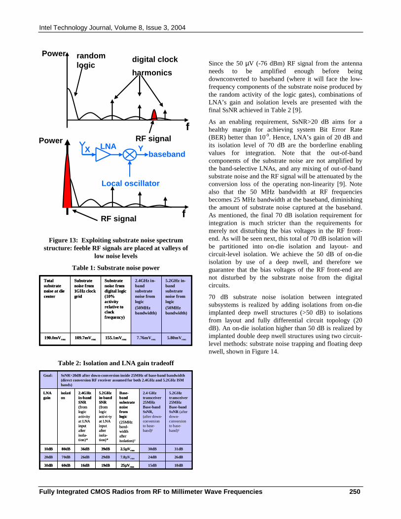
Intel Technology Journal, Volume 8, Issue 3, 2004
Fully Integrated CMOS Radios from RF to Millimeter Wave Frequencies 250
Figure 13: Exploiting substrate noise spectrum structure: feeble RF signals are placed at valleys of
low noise levels
Table 1: Substrate noise power
Table 2: Isolation and LNA gain tradeoff
Since the 50 µV (-76 dBm) RF signal from the antenna needs to be amplified enough before being downconverted to baseband (where it will face the low-frequency components of the substrate noise produced by the random activity of the logic gates), combinations of LNA’s gain and isolation levels are presented with the final SsNR achieved in Table 2 [9].
As an enabling requirement, SsNR>20 dB aims for a healthy margin for achieving system Bit Error Rate (BER) better than 10-9. Hence, LNA’s gain of 20 dB and its isolation level of 70 dB are the borderline enabling values for integration. Note that the out-of-band components of the substrate noise are not amplified by the band-selective LNAs, and any mixing of out-of-band substrate noise and the RF signal will be attenuated by the conversion loss of the operating non-linearity [9]. Note also that the 50 MHz bandwidth at RF frequencies becomes 25 MHz bandwidth at the baseband, diminishing the amount of substrate noise captured at the baseband. As mentioned, the final 70 dB isolation requirement for integration is much stricter than the requirements for merely not disturbing the bias voltages in the RF front-end. As will be seen next, this total of 70 dB isolation will be partitioned into on-die isolation and layout- and circuit-level isolation. We achieve the 50 dB of on-die isolation by use of a deep nwell, and therefore we guarantee that the bias voltages of the RF front-end are not disturbed by the substrate noise from the digital circuits.
70 dB substrate noise isolation between integrated subsystems is realized by adding isolations from on-die implanted deep nwell structures (>50 dB) to isolations from layout and fully differential circuit topology (20 dB). An on-die isolation higher than 50 dB is realized by implanted double deep nwell structures using two circuit-level methods: substrate noise trapping and floating deep nwell, shown in Figure 14.
RF signal
digital clock
harmonics
f
RF signal f
LNA
Local oscillator
baseband X Y
random logic
Power
Power
5.80mVrms7.76mVrms155.1mVrms109.7mVrms190.0mVrms
5.2GHz in-band substrate noise from logic(50MHz bandwidth)
2.4GHz in-band substrate noise from logic(50MHz bandwidth)
Substrate noise from digital logic (10% activity relative to clock frequency)
Substrate noise from 1GHz clock grid
Total substrate noise at die center
18dB
26dB
31dB
5.2GHz transceiver 25MHz Base-band SsNR (after down-conversion to base-band)‡
15dB
24dB
30dB
2.4 GHz transceiver 25MHz Base-band SsNR, (after down-conversion to base-band)‡
25µVrms19dB16dB60dB30dB
7.8µVrms29dB26dB70dB20dB
2.5µVrms39dB36dB80dB10dB
Base-band substrate noise from logic
(25MHz band-width after isolation)†
5.2GHz in-band SNR (from logic activi-tyat LNA input after isola-tion)*
2.4GHz in-band SNR (from logic activity at LNA input after isola-tion)*
isolation
LNA gain
SsNR>20dB after down-conversion inside 25MHz of base-band bandwidth (direct conversion RF receiver assumed for both 2.4GHz and 5.2GHz ISM bands)
Goal:
Intel Technology Journal, Volume 8, Issue 3, 2004
Fully Integrated CMOS Radios from RF to Millimeter Wave Frequencies 251
Figure 14: Deep nwell hook ups and biasing
The deep nwell covering the digital circuit section attenuates the substrate noise passing through the deep nwell’s walls towards the common substrate (substrate noise trapping). Once into the common substrate, the attenuated substrate noise will proceed towards the deep nwell protecting the RF circuit section, making that whole deep nwell change its electric potential uniformly (floating deep nwell). These two mechanisms are more effective the more conductive is the deep nwell implant in relation to the substrate, and the smaller the area of the floating deep nwell.
Figure 15: Differential signaling between analog and digital subsystems
In order to realize these two effects, the power supply for the subcircuits sections and signaling between the two sections follows the description in Figure 14 and 15. Note both Vcc and Vss power supply connections for both subcircuits are kept independent and never connected on-
die. Moreover, the signaling between the two subsections is differential. This differential signaling leaves the analog and digital subsystems to “fluctuate” relative to each other.
Figure 16: Double deep nwell isolation (aggressor and victim surrounded by nwell) vs. no deep nwell
isolation
The differential interface defines a preferred path for signals from one subsystem to another. Substrate noise from the digital subsystem will travel towards the analog subsystem through the common mode loop. Since this common mode loop has several choke inductors along its path, it will present a high impedance for currents (Figure 15) and will strongly attenuate the substrate noise sensed in the analog subsystem. This on-die isolation was analyzed using a commercial electromagnetic field solver. Isolation between subcircuits reaches 50 dB even for highly conductive (lossy) substrate (1x10³ S/m) with no epi-layer, and separation between analog and digital subcircuits as small as 200 µm. On-die isolation exceeds 50 dB if an epi-layer (5-125 S/m conductivity) is added in the field solver simulations, thus benefiting the state-of-art technology of high-performance logic CMOS technology.
Figure 16 shows results for 50 µm-thick deep nwell lateral walls, which is appropriate for subsystem isolation (not for individual transistor isolation). The 50 dB isolation levels for thick-wall double-deep nwell isolation (both aggressor and victim covered by deep nwells) and frequency characteristics agree with experimental results obtained by CMOS foundries later [27].
For the additional layout- and circuit-level isolation, RF circuits are fully differential with layout of matched devices based on a common centroid. Transistors sized with W=250 µm-460 µm (common in 2.4 GHz/5.2 GHz RF designs with 140 nm CMOS technology) Vt and Lmin mismatches lead to gm mismatches smaller than 10%, which imply >20 dB common-mode rejection. Once
p - n
RF circuit
section
digital circuit
section
Double deep
nwell isolation
Floating deep
nwell
Substrate noise
trapping nwell
Vss (analog)
Vcc (analog) Vss (digital)
Vcc (digital)
Vss (digital)
Common
substrate
p - n
p - p -
2.4 4.4 6.4 8.4 10 Frequency ( GHz)
-160
-140
-120
-100
-80
-60 S21 ( dB)
50 bare
double dnwell
Analog
Sub
Digital
Sub
Differential signal
interface
R
Analog
power + + Digital
power
low impedance
differential loop
high impedance common-mode loop
same-die housing
choke
choke
choke
choke
choke
Intel Technology Journal, Volume 8, Issue 3, 2004
Fully Integrated CMOS Radios from RF to Millimeter Wave Frequencies 252
substrate activity passes to the circuit signal lines with some attenuation, layout- and circuit-level isolation combined reaches above 20 dB as desired. An additional “vertical grid” was simulated in the electromagnetic field solver to minimize coupling between on-die metal traces, which imposes also an isolation higher than 70 dB for this path. This vertical grid was connected to the digital Vss and finally completed the total isolation enabling RF-digital processor integration.
Table 3: Body bias and RF performance
Due to the introduction of deep nwells, body biasing becomes an additional degree of freedom for both digital and RF circuits. Reverse and forward body bias, respectively, diminishes and augments the current driving capability (hence gm) of the devices as can be seen by the change in Ids with Vb in Table 3. However, as the current driving capability increases, the drain junction capacitance also increases as that junction becomes less reverse biased, and the overall effect is a diminishment in the RF performance with forward bias as represented by the measured |S21| in Table 3. That is a clear departure from the effect of body bias in digital circuitry where the capacitances at the output of logical gates are dominated by the gate capacitance of the following gate, and any increase in current-driving capability implies a gain in performance. Note also that, as expected, there is no apparent effect of body bias on the carrier heating (drain current excess thermal noise) by the high horizontal electric field in the channel as Fmin merely tracks variations in the device gain (|S21|) – higher |S21| (Table 3). Table 4 compares the behavior of identical transistors inside and outside the deep nwell. A small but perceptible increase in channel resistance diminishes the driving current capability, diminishes the RF performance (|S21|), augments Fmin, and augments Rn (the device in the deep nwell departs from the optimum noise performance faster with source impedance than the identical device outside the well). Nevertheless, these are not compromising effects. Similarly, from 25oC to 110oC the device performance inside and outside the deep nwell showed a less than 10% variation in RF and noise parameters.
Table 4: Transistor inside vs. outside deep nwell
Mixed-signal integration for high-performance System-on-a-Chip (SoC) is thus enabled with minimal technology modification, by adding deep nwell structures. By exploring the spectrum structure of the substrate noise of a high-performance microprocessor (1 GHz 55 W) with a clock at GHz frequencies, and placing the feeble RF signals (for a 50 MHz, –76 dBm-sensitivity receiver) received from the antenna between harmonics of the clock, we have shown that 70 dB of isolation is sufficient to enable RF-high-performance digital processor integration.
Note that this was an extreme case of RF and digital processor integration in the same die. RF delicate circuits are more likely to be integrated with sub 2 W digital circuits or processors, instead of 55 W and above digital processors. Therefore, less isolation between digital and RF circuits is likely to be the typical case and deep nwell structures might be only seldom used. Our investigation, accordingly, supported the feasibility of RF and digital processor integration in the same die with comfortable margins.
CMOS SYSTEM ON A PACKAGE (SOP) After digital substrate noise is successfully handled, silicon area availability is the next and final road block to be cleared in the path to RF and digital processor integration in the same die. Multiband radios do require a large number of passive components that take considerable area on-die and are also non-scaling components. This area road block will be adequately cleared in this section as a side effect of a creating high-performance wireless SoP.
Higher performance RF and microwave transceivers require high-performance active devices and high-quality passives. On the silicon die, only the former is available. Integrated passives have poor quality factors (Q), typically around 5 or 7 at low GHz frequencies. A significant improvement in such a scenario is found when passives are implemented on the package substrate. That’s because Q is a ratio of energy accumulated in the component to its losses per cycle of the operating frequency. Therefore, since energy is associated with the volume occupied by the electric and magnetic fields of
1.202.97960.58+0.500.70.7
1.143.12249.82+0.250.70.7
1.073.24835.36-0.250.70.7
1.053.25330.02-0.50.70.7
Fmin@ 5.2 GHz (dB)
|S21| @ 5.2 GHz
Id (mA)
Vb(V)
Vd(V)
Vg (V)
1.202.97960.58+0.500.70.7
1.143.12249.82+0.250.70.7
1.073.24835.36-0.250.70.7
1.053.25330.02-0.50.70.7
Fmin@ 5.2 GHz (dB)
|S21| @ 5.2 GHz
Id (mA)
Vb(V)
Vd(V)
Vg (V)
0.350.221.711.153.0363.33846.348.0
Rn/[email protected] GHz
(dnwell)(dB)
Rn/50
@5.2GHz(dB)
(dnwell)(dB)
[email protected] (dB)
|S21|@5.2 GHz
(dnwell)
|S21|@5.2GHz
Ids(dnwell)
(mA)
Ids(mA)
0.350.221.711.153.0363.33846.348.0
Rn/[email protected] GHz
(dnwell)(dB)
Rn/50
@5.2GHz(dB)
(dnwell)(dB)
[email protected] (dB)
|S21|@5.2 GHz
(dnwell)
|S21|@5.2GHz
Ids(dnwell)
(mA)
Ids(mA)

Intel Technology Journal, Volume 8, Issue 3, 2004
Fully Integrated CMOS Radios from RF to Millimeter Wave Frequencies 253
the passive component and the losses are predominantly associated with the surface of the conductors used in those passives at low GHz frequencies, just by being able to use more volume leads to higher quality passives. In this sense, the height from the bottom metal layer to the top metal layers in the silicon back-end is around 5 µm, whereas the metal layer separation on the package substrate is around 30 µm. Then, a 6X improvement in quality for the passives could be expected by moving a passive component from the silicon die to the low-cost package substrate. Unfortunately, dielectric losses on the package substrate (which uses organic materials) is significantly higher than the SiO2-based interlayer dielectric used on the die, and final quality factor improvement, though still realizable, is somehow lower than 6X [10].
Figure 17: Die and package metal stacking and dielectric separations
It is interesting to realize that despite being higher than on-die, the still relatively modest Qs of passives on the package warrant optimization of the final LNA design by backing off, explained earlier. In order to better appreciate this, Figure 18 shows that depending on the Q being 5 or 10 for inductors in the IMN, a floor of 1 dB noise figure for the LNA is already established if too-high inductor values are placed in that IMN. This means that transistors in the LNA need to be properly sized with the minimization of inductance in the IMN included. Note that according to Figure 18, for instance, for an LNA at 2.4 GHz it is necessary to use inductor values below 8.5 nH in the Q=10 curve, to have any chance of making a 1 dB noise figure LNA, even if the rest of the LNA is completely noiseless.
Similar benefits are accrued by other RF key components. Oscillators and VCOs also develop less phase noise if higher quality passive components are used, since all the noise contributors (not only transistor’s 1/f noise) influence phase noise, as was discussed in the 1/f section of this paper.
In RF Power Amplifiers (PAs), the moving of passives from the die to the package is not just a benefit but actually an enabling development. As CMOS transistors scale, less voltage swing is tolerated at their terminals,
and a high quality impedance converter needs to be placed between the antenna and transistors’ drain for high-power transmissions. High-quality impedance converters are just not available on-die. Moreover, the impedance converters solve the problem of high voltage swing by trading it for high current handling capabilities. This means the RF choke used in the PA of Figure 19 needs to carry currents on the 1A peak levels or more at times. For the sake of reliability, such wide metal traces have to be used on die to support these currents that the RF choke becomes plagued with parasitics and then it is useless even at low GHz frequencies. Moving the passives to the package neatly solves the problems of the high-quality impedance converter and the high-current handling capabilities of the RF choke.
Figure 18: Input-matching-network-limited LNA’s noise figure
Figure 19: Conceptual description of power amplifiers
Metal 6 to metal 1 separation ~ 5µm Back of wafer/die ~ 100-400µm
Metal layer separations ~ 30µm Package pins
M1
IM
L1
L2
RF in+ R1
C1
Vn ~
0 2 4 6 8 10 12 14 160
0.5
1
1.5
2
2.5
3
3.5
4
4.5
5
L1 (
NF
( dB)
NFIMN=f (L1, QL1, fop)
5.2
Q=5
Q=10
2.4 Q=5
Q=10 1 dB
M1 Impdnc
Trfrmr RF_out
Vcc V2/R V2/R
RFchoke
Intel Technology Journal, Volume 8, Issue 3, 2004
Fully Integrated CMOS Radios from RF to Millimeter Wave Frequencies 254
Figure 20 shows the area of a flip-chip package where passives can be realized by trace engineering (no discrete components added), and a 3D blowup of an example of moving impedance transformers and RF chokes to the package substrate. Figure 21 depicts the 1-to-1 correspondence between schematics and trace layout realization for the PA’s network of Figure 20.
Figure 20: High-quality RF passives realized by trace engineering on the flip-chip package substrate
More compact realizations of the PA’s network can be developed, and Figure 22 shows how a power combination of four identical PAs can be realized on-die, occupying a small area. The PA’s transmission power in the range of 0.5 W at 5.5 GHz can be readily achieved with low voltage (1.2 V) transistors.
Figure 21: Schematic and trace layout correspondence for a PA with its entire passive
network on the package substrate
Moving RF passives to the package substrate can be carried on to the extreme of moving all the big passives out of the silicon die and onto the package. Such a move is supported by the large pin count capability of flip-chip packages and ultimately will lead to leaving only the transistors on-die. Having only the radio’s transistors on-die makes the radio occupy only a small area in that die. Figure 23 shows a concept where all the radio’s passives are moved to the package surface and the radio becomes a slim area on the north side of the die. The rest of the die is now available to host a digital processor. Note that
given the already densely occupied processors and chipset dies, if we are to integrate radios into those dies, the radio needs to be of minimum area. Moving the passives to the package then becomes again an enabling technology.
Figure 22: Power combining of 4 PAs on the package: 0.5 W of power transmission with 1.2 V transistors
Figure 23: All-passives-on package radio concept. Radio becomes a slim silicon area north of the die,
and a general-purpose digital processor is hosted on the same die.
Another path for the SoP with all (or most of) the RF passives moved to the package substrate is explored later in this paper.
SIGMA-DELTA ADCS AND DACS: TRADING VOLTAGE RESOLUTION FOR TIME RESOLUTION Analog to Digital Converters (ADCs) and Digital to Analog Converters (DACs) are the specialty circuits at the interface between the RF front-end and the digital communication processing circuits. It is important to point out these analog specialty circuits are in fact influenced on the architecture and circuit level by CMOS scaling and the new requirements of high performance CMOS radios.
Antenna contacts
2.4 GHz dense transmission line serpentine
3.1cm
3.1cm
Die
~1cm
Antenna contacts
Area available
for circuit on k
Multi-layer
flip-chip
Impedance
M
M
Ms
Impdnc
Trfrmr
Impdnc
Trfrmr
Dipole antenna
RF_out +
RF_out -
Pa_on
RF chk1
RF chk2
Vcc
Vcc
tx1
tx2
d1
d2
Vcc
Impedance
Transformer 1 RF-choke1
RF-choke2
tx1
tx2
d1
d2
On-die
die
package
PA LNA Synth Mx Mx
General purpose processor (MAC, windows)
Mem buffer
5.2 GHz PA
2.4 GHz PA
5.2 GHz LNA passives
2.4 GHz LNA passives
2.4 GHz/5.2 GHz Synthesizer
All active devices on-die make for a thin area along the top die side
towards the dipole antenna
PA1PA2 PA3PA4
Silicon die
package
¼ wavelength transmission linesfor power combination at antenna
4 RF-chokes based on 4 ¼ wavelength transmission lines
Impedance transformers
towards the dipole antenna
PA1PA2 PA3PA4
Silicon die
package
towards the dipole antenna
PA1PA2 PA3PA4
Silicon die
towards the dipole antenna
PA1PA2 PA3PA4
Silicon die
package
¼ wavelength transmission linesfor power combination at antenna
4 RF-chokes based on 4 ¼ wavelength transmission lines
Impedance transformers
Intel Technology Journal, Volume 8, Issue 3, 2004
Fully Integrated CMOS Radios from RF to Millimeter Wave Frequencies 255
As CMOS scales, lower voltages and integrated components variations (mismatches) become higher and higher barriers for voltage resolution. Fortunately, scaling delivers higher and higher speeds in the circuits and enables large oversampling ratios for both ADCs and DACs operations. Large oversampling ratios allow for a directly proportional diminishment in (kT/C)-limited (thermal noise limited) capacitor sizes used in switching circuits [28, 29]. Clever high oversampling circuit techniques can make systematic offset produced by mismatch in the components show up as high-frequency noise, which can be readily filtered in order to achieve a high number of bits resolution. Oversampling also alleviates the anti-aliasing analog filtering order prior to the ADC blocks, and quantization noise can be shaped so that its frequency content is higher away from the frequencies of interest for the information being processed [30].
More importantly, radio signals are bandpass in nature. Before downconversion to baseband, those signals are made of a narrow band information signal on a higher frequency carrier. These signals can appropriately be tackled with sigma-delta ADCs and DACs, in particular the bandpass version of these, where all the benefits mentioned above for trading off voltage resolution for time resolution are at the core of these converter concepts. Oversampling ratios can reach values well above 50 (bandpass signal width to sampling frequency) [28, 29].
It is important to relate this change in gears for ADC and DAC converters due to CMOS scaling to a disruptive effect in radio transceiver architecture: these new ADCs and DACs allow for simplified RF front-ends and synthesizers in multiband multiprotocol radios. That is because the RF front-end will not, for instance, chase the narrow channels anymore during communications as defined by 802.16. Chasing narrow channels is now moved to the digital domain, since high-speed ADCs support a much larger bandwidth to be processed in the receiver, and high-speed DACs allow for offsetting signals for proper channelization prior to sending them to the RF transmitter.
Flexible Radios: a Practical Vision The CMOS-based computer industry takes full advantage of CMOS scaling to produce always changing ever more powerful computing platforms. This was thought to be in fundamentally stark contrast to the standards-driven communications industry.
Figure 24: Flexible radios: a PC platform for merging computing and communications under always-
evolving communication standards
Despite that, the reality of recent years and plans for the foreseeable future appear to show a path for further integration of computing and communications. The apparent paradox disappears when one considers communication standards are always evolving documents.
The standards themselves generate new standards and addenda to standards are always being made. Standards serve as guidelines for products, and these products at a given time only attend to a limited subset of recommendations in the standards to warrant a compatibility stamp like “Wi-Fi” or “WiMAX.” Other parts of the standards are left for future implementation. In such a state of affairs, computing and communications do share the always-evolving aspects that are the spirit of the CMOS business model.
At the implementation level, multiband, multiprotocol radio for always-evolving communication standards is too complex a system to fit in a Pentium or chipset die. It would be probably better to start thinking that the PC motherboard will be a multiprocessor platform whose ecosystem will be populated by new chips besides the Pentium and chipset.
Figure 24 illustrates in a highly simplified abstraction the addition of a flexible radio to a multiprocessor PC platform. Note the suggestion that Intel® XScale® technology should become the general-purpose processor to handle all aspects of reprogrammability and hardware switchability of the flexible radio. XScale would be also in charge of a software-MAC (for easy reprogrammability) and all network layers of operation for the radio.
Figure 25 depicts a flexible radio concept and its realization as one package and two silicon chips. This concept exploits all the CMOS technology and package
® Intel XScale is a registered trademark of Intel Corporation or its subsidiaries in the United States and other countries.
XScale cores
DSP+RF
open standard
P4
chipset
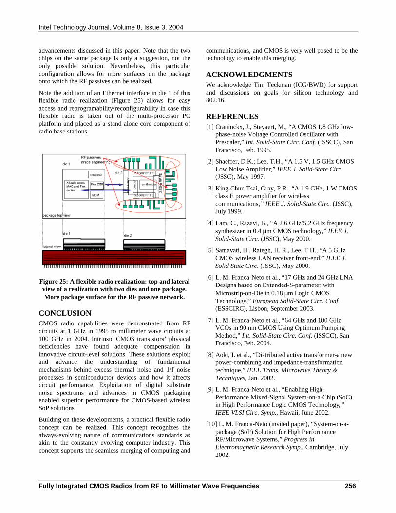
Intel Technology Journal, Volume 8, Issue 3, 2004
Fully Integrated CMOS Radios from RF to Millimeter Wave Frequencies 256
advancements discussed in this paper. Note that the two chips on the same package is only a suggestion, not the only possible solution. Nevertheless, this particular configuration allows for more surfaces on the package onto which the RF passives can be realized.
Note the addition of an Ethernet interface in die 1 of this flexible radio realization (Figure 25) allows for easy access and reprogramability/reconfigurability in case this flexible radio is taken out of the multi-processor PC platform and placed as a stand alone core component of radio base stations.
Figure 25: A flexible radio realization: top and lateral view of a realization with two dies and one package. More package surface for the RF passive network.
CONCLUSION CMOS radio capabilities were demonstrated from RF circuits at 1 GHz in 1995 to millimeter wave circuits at 100 GHz in 2004. Intrinsic CMOS transistors’ physical deficiencies have found adequate compensation in innovative circuit-level solutions. These solutions exploit and advance the understanding of fundamental mechanisms behind excess thermal noise and 1/f noise processes in semiconductor devices and how it affects circuit performance. Exploitation of digital substrate noise spectrums and advances in CMOS packaging enabled superior performance for CMOS-based wireless SoP solutions.
Building on these developments, a practical flexible radio concept can be realized. This concept recognizes the always-evolving nature of communications standards as akin to the constantly evolving computer industry. This concept supports the seamless merging of computing and
communications, and CMOS is very well posed to be the technology to enable this merging.
ACKNOWLEDGMENTS We acknowledge Tim Teckman (ICG/BWD) for support and discussions on goals for silicon technology and 802.16.
REFERENCES [1] Craninckx, J., Steyaert, M., “A CMOS 1.8 GHz low-
phase-noise Voltage Controlled Oscillator with Prescaler,” Int. Solid-State Circ. Conf. (ISSCC), San Francisco, Feb. 1995.
[2] Shaeffer, D.K.; Lee, T.H., “A 1.5 V, 1.5 GHz CMOS Low Noise Amplifier,” IEEE J. Solid-State Circ. (JSSC), May 1997.
[3] King-Chun Tsai, Gray, P.R., “A 1.9 GHz, 1 W CMOS class E power amplifier for wireless communications,” IEEE J. Solid-State Circ. (JSSC), July 1999.
[4] Lam, C., Razavi, B., “A 2.6 GHz/5.2 GHz frequency synthesizer in 0.4 µm CMOS technology,” IEEE J. Solid-State Circ. (JSSC), May 2000.
[5] Samavati, H., Rategh, H. R., Lee, T.H., “A 5 GHz CMOS wireless LAN receiver front-end,” IEEE J. Solid State Circ. (JSSC), May 2000.
[6] L. M. Franca-Neto et al., “17 GHz and 24 GHz LNA Designs based on Extended-S-parameter with Microstrip-on-Die in 0.18 µm Logic CMOS Technology,” European Solid-State Circ. Conf. (ESSCIRC), Lisbon, September 2003.
[7] L. M. Franca-Neto et al., “64 GHz and 100 GHz VCOs in 90 nm CMOS Using Optimum Pumping Method,” Int. Solid-State Circ. Conf. (ISSCC), San Francisco, Feb. 2004.
[8] Aoki, I. et al., “Distributed active transformer-a new power-combining and impedance-transformation technique,” IEEE Trans. Microwave Theory & Techniques, Jan. 2002.
[9] L. M. Franca-Neto et al., “Enabling High-Performance Mixed-Signal System-on-a-Chip (SoC) in High Performance Logic CMOS Technology,” IEEE VLSI Circ. Symp., Hawaii, June 2002.
[10] L. M. Franca-Neto (invited paper), “System-on-a-package (SoP) Solution for High Performance RF/Microwave Systems,” Progress in Electromagnetic Research Symp., Cambridge, July 2002.
Intel Technology Journal, Volume 8, Issue 3, 2004
Fully Integrated CMOS Radios from RF to Millimeter Wave Frequencies 257
[11] S. Sze, Physics of Semiconductor Devices, Wiley Inter Science, 2nd ed., 1981.
[12] L. M. Franca-Neto, “Noise in High Electric Field Transport: the Ergodic Method,” Ph.D. Thesis, Stanford University, 1999.
[13] R. E. Collin, Foundations of microwave engineering, 2nd ed., McGraw Hill, 1992.
[14] IEEE 802.16 standard.
[15] B. Razavi, RF Microelectronics, Prentice Hall, 1998.
[16] Farjad-Rad, R. et al., “A low-power multiplying DLL for low-jitter multigigahertz clock generation in highly integrated digital chips,” IEEE J. Solid-State Circ. (JSSCC), Dec. 2002.
[17] B. Razavi, “A Study of Phase Noise in CMOS Oscillators,” IEEE J. Solid-State Circ. (JSSC), March 1996.
[18] A. Hajimiri, T.H. Lee, “A General Theory of Phase Noise in Electrical Oscillators,” IEEE J. Solid-State Circ. (JSSC), Feb. 1998.
[19] A. Hajimiri, T.H. Lee, “Phase Noise in CMOS Differential LC Oscillators,” IEEE VLSI Symp on Circ., 1996.
[20] A. Hajimiri et al., “Phase Noise in Multi-Gigahertz CMOS Ring Oscillators,” IEEE Custom Integrated. Circ. Conf. (CICC), 1998.
[21] Rael, J.J., Abidi, A. A., “Physical Processes of Phase Noise in Differential LC Oscillators,” IEEE Custom Integrated. Circ. Conf. (CICC), 2000.
[22] T. H. Lee, The Design of CMOS Radio-Frequency Integrated Circuits, Cambridge University Press, 1998.
[23] G. D. Vendelin, A. M. Pavio, and U. L. Rohde, Microwave Circuit Design using Linear and Nonlinear Techniques, John Wiley, 1990.
[24] I. Bahl and P. Bhartia, Microwave Solid State Circuit Design, John Wiley, 1988.
[25] Applied Wave Research, http://www.awr.com.*
[26] M. van Heijningen et al., “Substrate noise generation in complex digital systems: efficient modeling and simulation methodology and experimental verification,” Int. Solid State Circ. Conf. (ISSCC), San Francisco, Feb. 2001.
[27] TSMC documents.
[28] B. Leung, VLSI for wireless communications, Prentice Hall, 2002.
[29] J. C. Candy and G. C. Temes, Oversampling Delta-Sigma Data Converters: theory, design and simulation, Wiley Inter-Science, 1992.
[30] R. van de Plassche, CMOS integrated Analog-to-Digital and Digital-to-Analog converters, 2nd ed., Kluwer, 2003.
AUTHORS’ BIOGRAPHIES Luiz M. Franca-Neto earned his Electronic Engineering degree, with distinction, from ITA/CTA, SJC, Sao Paulo, Brazil, in 1989, and he received the TASA award for being first in class in communications. He received his M.Sc. and Ph.D. degrees from Stanford University, all in Electrical Engineering, in 1995 and 1999, respectively. From 1990 to 1992, he was a design engineer with ALCATEL/Elebra Telecom for public telecommunications and optical line terminal equipment. In USA from 1993-1996, he has worked for HP-Labs, Palo Alto, CA, and Texas Instruments, Dallas, TX. He was with Intel R&D Labs from 1999-2004, where he led research on CMOS for RF/Microwave/Millimeter wave frequencies. He created new circuit design methods such as “backing off” for LNAs and “optimum pump” for VCOs with demonstrated circuits operating from 2.4 GHz to 100 GHz (a world record for CMOS). He led the investigations for substrate noise in Pentium 4 processors and deep nwell isolation where he articulated how substrate noise spectrum structure can be exploited for full integration of digital processors and RF delicate circuits in the same die. Also in the labs, Luiz led the research to move all RF passives from the die to the substrate package in order to realize higher performance RF System-on-Package and free silicon area for hosting more digital functions and general-purpose processors. Since February 2004, Luiz has led the WiMAX RF & Analog IC internal development within the ICG/BWD group in Santa Clara. His homepage is http://www-snow.stanford.edu/~franca.*
Roger Eline received a B.S.E.E. degree from UC Davis and an M.S.E.E from Santa Clara University in 1991. Since then his work has focused on RF and microwave communication system development. He currently works for the BroadBand Wireless Division of Intel, where he manages the Platform Engineering Group. He has been with Intel for one and a half years developing low-cost IEEE 802.16 baseband and radio reference platforms based on Intel’s IEEE 802.16 baseband processor/modem ASIC. His e-mail is Roger.j.eline at intel.com.
Balvinder Bisla received his B.Sc. degree at Sussex University, England in 1984. He then worked at Rutherford Appleton Labs in the UK before moving to the USA to work on wireless metering and global
Intel Technology Journal, Volume 8, Issue 3, 2004
Fully Integrated CMOS Radios from RF to Millimeter Wave Frequencies 258
positioning systems. He was a principal RF engineer with Iospan Wireless where they developed the world’s first MIMO-OFDM system. Currently he is working at Intel on RF and microwave communication issues for WiMAX products. His e-mail is Balvinder.s.Bisla at intel.com.
Copyright © Intel Corporation 2004. This publication was downloaded from http://developer.intel.com/.
Legal notices at http://www.intel.com/sites/corporate/tradmarx.htm.

Copyright © 2004 Intel Corporation. All rights reserved.Intel is a trademark or registered trademark of Intel Corporation or its subsidiaries in the United States and other countries. For a complete listing of trademark information visit: www.intel.com/sites/corporate/tradmarx.htm
For further information visit:
developer.intel.com/technology/itj/index.htm