Embed Size (px)
Citation preview

UNLV Retrospective Theses & Dissertations
1-1-2005
Interaction between palladium and silicon carbide: A study for Interaction between palladium and silicon carbide: A study for
Triso nuclear fuel Triso nuclear fuel
Goverdhan Reddy Gajjala University of Nevada, Las Vegas
Follow this and additional works at: https://digitalscholarship.unlv.edu/rtds
Repository Citation Repository Citation Gajjala, Goverdhan Reddy, "Interaction between palladium and silicon carbide: A study for Triso nuclear fuel" (2005). UNLV Retrospective Theses & Dissertations. 1935. http://dx.doi.org/10.25669/pt1i-m112
This Thesis is protected by copyright and/or related rights. It has been brought to you by Digital Scholarship@UNLV with permission from the rights-holder(s). You are free to use this Thesis in any way that is permitted by the copyright and related rights legislation that applies to your use. For other uses you need to obtain permission from the rights-holder(s) directly, unless additional rights are indicated by a Creative Commons license in the record and/or on the work itself. This Thesis has been accepted for inclusion in UNLV Retrospective Theses & Dissertations by an authorized administrator of Digital Scholarship@UNLV. For more information, please contact [email protected].

INTERACTION BETWEEN Pd AND SiC: A STUDY FOR TRISO NUCLEAR FUEL
by
Goverdhan Reddy Gajjala
Bachelor of Science in Electrical Engineering Osmania University College of Engineering, India
April 2003
A thesis submitted in partial fulfillment of the requirements for the
Master of Science Degree in Engineering Department of Electrical & Computer Engineering
Howard R. Hughes College of Engineering
Graduate College University of Nevada, Las Vegas
May 2006
Reproduced with permission of the copyright owner. Further reproduction prohibited without permission.

UMI Number: 1436748
INFORMATION TO USERS
The quality of this reproduction is dependent upon the quality of the copy
submitted. Broken or indistinct print, colored or poor quality illustrations and
photographs, print bleed-through, substandard margins, and improper
alignment can adversely affect reproduction.
In the unlikely event that the author did not send a complete manuscript
and there are missing pages, these will be noted. Also, if unauthorized
copyright material had to be removed, a note will indicate the deletion.
UMIUMI Microform 1436748
Copyright 2006 by ProQuest Information and Learning Company.
All rights reserved. This microform edition is protected against
unauthorized copying under Title 17, United States Code.
ProQuest Information and Learning Company 300 North Zeeb Road
P.O. Box 1346 Ann Arbor, Ml 48106-1346
Reproduced with permission of the copyright owner. Further reproduction prohibited without permission.

Thesis ApprovalThe Graduate College University of Nevada, Las Vegas
A p r il 3 . 2006
The Thesis prepared by
Goverdhan G a jja la
Entitled
" in te r a c t io n Between Pd and SiC; A Study fo r
TRISO N u clear Fuel"
is approved in partial fulfillment of the requirements for the degree of
______________ M aster o f S c ie n c e in E l e c t r i c a l E n g in eer in g
Examination ComMttee Member
_________________Exam inatio/ Committee Member
Graduate College Faculty Representative
Examination CorrpntfEfe Chair
Dean o f the Graduate College
11
Reproduced with permission of the copyright owner. Further reproduction prohibited without permission.

ABSTRACT
Interaction between Pd and SiC: A Study for TRISO Nuclear Fuel
by
Goverdhan Reddy Gajjala
Dr. Rama Venkat, Examination Committee Chair Professor & Chair of Electrical & Computer Engineering
University of Nevada, Las Vegas and
Dr. Clemens Heske, Examination Committee Chair Assoc. Professor, Dept, of Chemistry
University of Nevada, Las Vegas
The unique properties of SiC (wide band gap, high thermal conductivity, high
electron mobility, and resistance to radiation effects) permits it to operate reliably at very
high temperatures even in harsh environments and as coating layers in TRISO nuclear
fuels. To optimize the SiC for use as a coating material in the nuclear reactor fuel design,
it is important to elucidate the chemical bonding and interface formation of metal fission
products (Pd, Ag, Cs, etc.) with SiC coating layers and to study the diffusion behavior of
fission products into TRISO coating materials. It is known in the TRISO community that
Pd is able to corrode the SiC layer. However, the detailed nature of this corrosion is still
unknown.
The objective of this thesis is to study the influence of fission products (Pd) on the
chemical and electronic properties of the SiC coating layer in TRISO nuclear fuel
particles. For this purpose, three series of interfaces (Pd/SiC) were prepared and studied
111
Reproduced with permission of the copyright owner. Further reproduction prohibited without permission.
using X-ray Photoelectron Spectroscopy (XPS) and Ultraviolet Photoelectron
Spectroscopy (UPS).
The experimental approach comprises the preparation of Pd/SiC interfaces in-situ in
our ultra-high vacuum system by electron-beam deposition of Pd onto suitable prepared
SiC single crystal surfaces. In order to understand the impact of the SiC surface
properties on the interface formation, a variety of surface preparation and modification
schemes were employed. The results obtained give detailed information about the Pd/SiC
interface formation. Thereby the study shows a diffusion at this interface, which is an
important first step in understanding the corrosion of the SiC-layer in the TRISO
particles.
IV
Reproduced with permission of the copyright owner. Further reproduction prohibited without permission.

TABLE OF CONTENTS
ABSTRACT............................................................................................................................. iii
LIST OF FIGURES................................................................................................................vii
ACKNOWLEDGMENTS....................................................................................................... ix
CHAPTER I INTRODUCTION...........................................................................................11.1 TRISO fuel particle.................................................................................................. 11.2 Basis for the present study...................................................................................... 4
CHAPTER 2 LITERATURE REVIEW...............................................................................52.1 SiC surface studies................................................................................................... 52.2 Mechanisms of Pd-SiC interaction....................................................................... 8
2.2.1 Behavior of Pd in UO2 kernels........................................................................92.2.2 Influence of kernel composition...................................................................112.2.3 Concentration dependence ........................................................................... 122.2.4 Behavior in conjunction with rare earth fission products.......................... 122.2.5 Influence of the SiC properties.....................................................................13
CHAPTER 3 EXPERIMENTAL.........................................................................................153.1 Measuring methods................................................................................................ 15
3.1.1 X-ray Photoelectron Spectroscopy (XPS)...................................................173.1.2 Ultraviolet Photoelectron Spectroscopy (UPS).......................................... 183.1.3 Auger-Electron Spectroscopy (AES)........................................................... 19
3.2 Instrumentation ..............................................................................................193.2.1 Ultra High Vacuum (UHV)......................................................................... 203.2.2 Sample Handling............................................................................................213.2.3 Sample treatment...........................................................................................223.2.4 X-Ray Source.................................................................................................233.2.5 Concentric Hemispherical Analyzer (CHA)............................................... 253.2.6 Electron detector........................................................................................... 263.2.7 E-beam metal evaporator..............................................................................26
CHAPTER 4 RESULTS AND DISCUSSIONS................................................................284.1 Experimental series 1............................................................................................ 294.2 Experimental series 2 ............................................................................................ 324.3 Experimental series 3 ............................................................................................ 474.4 Discussions............................................................................................................ 58
Reproduced with permission of the copyright owner. Further reproduction prohibited without permission.

4.4.1 Sample state after the sputtering cycles........................................................604.4.2 After the Pd deposition steps....................................................................... 61
CHAPTER 5 CONCLUSIONS AND FUTURE WORK.................................................. 655.1 Conclusions........................................................................................................... 655.2 Future Work.......................................................................................................... 67
BIBLIOGRAPHY....................................................................................................................65
V ITA ........................................................................................................................................ 71
VI
Reproduced with permission of the copyright owner. Further reproduction prohibited without permission.

LIST OF FIGURES
Figure I-I TRISO fuel concept showing the fuel particles, fuel compacts, and fuelassembly blocks [6].........................................................................................3
Figure 2-1 Low energy electron diffraction (LEED) pattern recorded for selected surface structures at 95 eV electron energy: the pure (3 x 3), (3 x 3) with already dominating (2 x 2)c, pure (2 x 2)c. (Blackindicates high electron intensities) [16].........................................................6
Figure 2-2 Schematic representation of the corrosion mechanism of the TRISOSiC layer by the fission product palladium [7]............................................. 8
Figure 2-3 Pd penetration rate into SiC based on international data [25]........................... 11Figure 2-4 Pd penetration rate into SiC as a function of SiC coating rate [8].................... 14Figure 3-1 Schematic diagram of core-level ionization (photoemission) in a
semiconductor. The two competing secondary processes for filling the core hole (Auger-electron and X-ray emission) are also sketched. Solid arrows correspond to electrons, dashed arrows tophotons [29]................................................................................................... 16
Figure 3-2 SiC survey spectrum....................... 18Figure 3-3 Picture of the ESCA in the Chemistry Dept, UNLV.........................................20Figure 3-4 Concentric Hemispherical Analyzer (CHA)......................................................26Figure 3-5 The e-beam metal evaporator and its various parts...........................................27Figure 4-1 Survey spectrum of the as-introduced SiC sample of series 1.........................29Figure 4-2 Peak fit analysis of the C Is peaks before and after Pd deposition on
6H-SiC(0001). The C Is Species shown are (a) a bulk species, (b) a surface species before Pd deposition and (a) a bulk species, (b)an interface species, and (c) a reacted species after Pd deposition............31
Figure 4-3 Peak fit analysis of Si 2p. Before Pd deposition (a) a bulk species and (b) a surface species are found; after Pd deposition, (a) a surfacespecies and (b) an interface species are shown...........................................32
Figure 4-4 Sequence of survey spectra from series 2........................................................... 33Figure 4-5 C Is XPS spectra from series 2............................................................................ 34Figure 4-6 Peak fit analysis of the C Is spectra.................................................................... 35Figure 4-7 Area percentages of all three C Is species of the second series........................36Figure 4-8 Si 2p XPS spectra, second series......................................................................... 37Figure 4-9 Peak fit analysis of the Si 2p spectra, second series...........................................38Figure 4-10 Percent area plot of the Si 2p species................................................................ 39Figure 4-11 Pd 3da/2 spectra as a function of deposition step.............................................. 40Figure 4-12 Comparison of Pd 3d3/2 peaks for the thickest and thinnest Pd film............... 40Figure 4-13 Relative binding energy change in the peak positions of C Is, Si 2p,
and Pd 3d3/2....................................................................................................42
Vll
Reproduced with permission of the copyright owner. Further reproduction prohibited without permission.

Figure 4-14 Sequence of UPS survey spectra for the second series, taken with a bias voltage of 15 V and not taking the work function of theelectron analyzer into account......................................................................43
Figure 4-15 Secondary electron cut-off spectra of the second sample series..................... 44Figure 4-16 Au reference spectrum. ................................................................................... 44Figure 4-17 Upper valence band spectra of the second sample series................................ 45Figure 4-18 Position of the valence band maximum/Fermi edge for the second
sample series.................................................................................................. 46Figure 4-19 Work Function plot of the sample......................................................................46Figure 4-20 Sequence of XPS survey spectra of series 3..................................................... 47Figure 4-21 Sequence of C Is XPS spectra........................................................................... 48Figure 4-22 P e ^ fit analysis of C Is spectra........................................................... 49Figure 4-23 Area percentages of all three species of Cls, third series.......................... 50Figure 4-24 Si 2p XPS spectra, third series........................................................................... 51Figure 4-25 Peak fit analysis of the Si 2p spectra. Before Pd deposition, (a) bulk,
(b) surface species; and after Pd deposition, (a) surface, (c) interface species are seen. An additional species (d) can also beseen after the last deposition step.................................................................52
Figure 4-26 Percent area plot of Si 2p, third series............................................................... 53Figure 4-27 Pd 3d3/2 spectra as a function of Pd deposition.................................................53Figure 4-28 Relative change in the peak positions of C Is, Si 2p, and Pd 3d3/2.................54Figure 4-29 Sequence of UPS survey spectra for the third series, taken with a bias
voltage of 15 V and not taking the work function of the electronanalyzer into account.....................................................................................55
Figure 4-30 Secondary electron cut-off spectra of the third sample series.........................56Figure 4-31 Upper valence band spectra o f the third series................................................. 56Figure 4-32 Position of the valence band maximum/Fermi edge for the third
sample series.................................................................................................. 57Figure 4-33 Work Function plot of the sample at each step.................................................58Figure 4-34 Formation of a Schottky barrier (for the case of metal with a larger
work function than the semiconductor, as in the present case)................. 59Figure 4-35 Band scheme of the sample after sputter-cleaning........................................... 61Figure 4-36 Band scheme of the Pd-SiC interface after the U‘ Pd deposition....................62Figure 4-37 Band scheme of the Pd-SiC interface after further Pd deposition.................. 64
Vlll
Reproduced with permission of the copyright owner. Further reproduction prohibited without permission.

ACKNOWLEDGMENTS
I would like to dedicate this thesis to my parents, brother, Sandhya and friends whose
love, support and understanding have always motivated me to strive for excellence.
I would like to sincerely and wholeheartedly thank Dr. Clemens Heske for his
guidance and kindness throughout this work. His patience as an advisor, boundless
energy while teaching, promptness while reviewing all my writing, and passion for
research are to be commended and worth emulating. 1 am indebted to him for cajoling me
into doing experiments and 1 owe most o f this work to him.
1 am very grateful to my advisor. Dr. Rama Venkat, Chair o f Electrical and Computer
Engineering, for his extreme support and the valuable guidance he provided during this
project.
A special thanks and appreciation to our group, Lothar Weinhardt, Timo Hofinann,
Varun Marepally, Marcus Baer, Moni Blum, Jared White, and Kyle George who helped
me a lot throughout this work.
IX
Reproduced with permission of the copyright owner. Further reproduction prohibited without permission.

CHAPTER 1
INTRODUCTION
Two distinct nuclear processes involving the nuclei of atoms for energy production
are; fission—the splitting of a nucleus—and fusion—the joining together of two nuclei.
For any given mass or volume of fuel, nuclear processes generate more energy than can
be produced through any other fuel-based approach. In the case of nuclear fission, in
which the nucleus of an atom splits into two or more smaller nuclei (fission products),
heat and then electricity is generated from the energy released.
Fission power currently provides about 17 percent of the world’s electric power.
However, several problems like disposal of radioactive waste, concern about nuclear
weapons proliferation, concern about safe operation of plants, and failure mechanisms of
the nuclear fuel question fission’s potential as an acceptable power source today and in
the future [I].
1.1 TRISO fuel particle
The TRISO-coated fuel particles consist of a microspherical kernel of a radius -175
pm made of oxide or oxycarbide fuel and a coating made of porous pyrolytic carbon
(PyC), an inner layer made of dense PyC (IPyC), a silicon carbide layer (SiC), and an
outer layer made of dense PyC (OPyC) as shown in Figure I-l . The function of these
coating layers is to retain fission products within the particle. The porous PyC coating
1
Reproduced with permission of the copyright owner. Further reproduction prohibited without permission.

layer, called the buffer layer, attenuates fission recoils and provides void volume for
gaseous fission products and carbon monoxide. The IPyC coating layer acts as
containment to gases during irradiation and protects the fuel kernel from the reaction with
the coating gases during the SiC coating process. The SiC coating layer provides
mechanical strength for the particle and acts as a barrier to the diffusion of metallic
fission products, which diffuse easily through the IPyC layer. Finally, the OPyC coating
layer protects the SiC coating layer mechanically [2].
The SiC layer provides the primary barrier for both radioactive elements in the kernel
and gaseous and metallic fission products. Corrosion or thinning of the SiC lead to a
fracture of the coating layers or provide a localized path for the escape of fission products
by diffusion from the fuel particle. These radionuclides might reach the cooling circuit,
and ultimately result in maintenance and safety problems. So, the performance of these
fuel particles is a key component in system containment and depends heavily on the
properties and performance of the silicon carbide layer [3-5].
Reproduced with permission of the copyright owner. Further reproduction prohibited without permission.

Pyrolytic Carbon Silicon Carbide
Portxis Carbon Bufbr Oxide Fuel (TRUO, %} } TRISO Coating
PARTXGLm# COMPACT» PUCL «JIM INTSFigure 1-1 TRISO fuel concept showing the fuel particles, fuel compacts, and fuel
assembly blocks [6].
Chemical interaction of the SiC coating layer with fission products is one of the
possible performance limitations of the TRISO-coated fuel particles. Corrosion of the SiC
layers by the fission product palladium (Pd) has been observed in irradiated TRISO-
coated fuel particles [7-9]. The Pd-SiC interaction can degrade the capability of retaining
fission products within the particle. Moreover, once the SiC coating is breached by the
release of palladium, other hazardous fission products, such as Cs, Ag, and Sr can be
released from the fuel particles. The degradation of the SiC layer is considered to be one
of the main factors leading to coating failure. Besides the irradiation experiments, post
irradiation heating tests of the coated particles and out-of-reactor experiments on the Pd-
SiC interactions have been reported. But the mechanism of the corrosion of the SiC layer
Reproduced with permission of the copyright owner. Further reproduction prohibited without permission.

by palladium has not been understood clearly and data on the Pd-SiC interaction in UO2
fuel particles was limited [10].
1.2 Basis for the present study
The goal of this project is to elucidate the chemical bonding and the interface
formation of metal fission products (palladium) with the coating materials (SiC) so that
this helps in prevention of the release of fission products out of nuclear fuels.
Surface- and interface-sensitive spectroscopic methods like X-ray Photoelectron
Spectroscopy (XPS) and Ultraviolet Photoelectron Spectroscopy (UPS) were used to
elucidate the chemical nature of the interface between Pd and SiC [11]. This study adds a
new point of view to the existing discussion on the SiC coating layer in TRISO nuclear
fuels, because it gives a direct insight into the electronic structure and hence into the
nature of the chemical bonding at the interface. It sheds light on the chemical stability of
TRISO particles with respect to diffusion of Pd through the SiC coating material layer
and the corresponding interface. Based on a detailed analysis of the interface properties,
surface and interface modification treatments for an enhanced stability of TRISO-fuel
particles can be proposed in the future.
A literature review of the relevant work related to SiC surface study and corrosion of
SiC by Pd in nuclear fuels will be presented in Chapter 2. The experimental setup and
procedures for measuring, cleaning of the sample (SiC) by sputtering and annealing, and
deposition of Pd on SiC will be described in Chapter 3. Results and discussions will be
presented in Chapter 4. A summary of this thesis and recommendations for future
experiments are given in Chapter 5.
Reproduced with permission of the copyright owner. Further reproduction prohibited without permission.

CHAPTER 2
LITERATURE REVIEW
The properties of SiC, such as wide band gap, high thermal conductivity, high
electron mobility, and resistance to radiation effects make it a desirable semiconductor
for high temperature operations, high power microelectronics, as well as for coating
layers in TRISO nuclear fuels. These unique properties permit SiC to operate reliably at
very high temperatures even in harsh environments. A detailed literature study about the
SiC surfaces and the chemical interactions of fission products with TRISO particles is
given in this chapter. To compare with the literature results, note that the SiC single
crystal surface that was used for this work was 6H-SiC(000I).
2.1 SiC surface studies
Many polytypes of SiC (e.g., 3C-, 4H - and 6H-SiC) exist, differing only in the
stacking sequence of the hexagonal bilayers of alternating silicon and carbon atoms [12].
The clean surfaces of 3C-, 4H- and 6H-SiC are strongly reconstructed and have different
structures depending on how the surface was prepared. For example, in the case of 6H-
SiC(OOOI)-Si (Si-terminated), the surface can show three different types of
reconstructions: (i) 3x3, (ii) V3xV3 and (iii) 6x6 [13]. Aimealing the Si-predeposited
surface at 850 °C in ultra-high vacuum (UHV) leads to a 3x3 surface, which is changed
Reproduced with permission of the copyright owner. Further reproduction prohibited without permission.

to a VSxVs reconstruction by further annealing at 950 °C. Further heating above 1000°C
forms a ôVSxôVs structure. When the (0001) surface is flashed to 1150 °C, it is
graphitized and takes a 6x6 structure. It is believed that the bVSxbVS surface is a mixture
of the VSxVs and 6x6 domains [14]. The 6H-SiC(000I)- VSxVs surface consists of Si
adatoms of 1/3 of a monolayer on top of the Si-C bilayer. It was also found that the
SiC(OOOI)-3x3 surface comprises the silicon adatoms supported by trimers on the Si
adlayer which is located on the first Si-C bilayer. This indicates that the oxidized surface
structure is not homogeneous and SiOa-like domains accompanied by some SiCxOy
silicate with a C -0 bond are formed [15].
a) 0%3) b ) f2x2)c& C) (2'2)c(3x3)
• . . .
# ' ' #
95 eV 95 eV 95 eV
Figure 2-1 Low energy electron diffraction (LEED) pattern recorded for selected surface
structures at 95 eV electron energy: the pure (3 x 3), (3 x 3) with already dominating (2 x
2)c, pure (2 x 2)c. (Black indicates high electron intensities) [16].
Bernhardt et al. investigated the initial oxidation of the 6H-SiC(0001)-V3xV3 surface
was analyzed in-situ by medium energy ion scattering and synchrotron-based
photoelectron spectroscopy, to determine the absolute quantity of adsorbed oxygen and
Reproduced with permission of the copyright owner. Further reproduction prohibited without permission.

measure the fraction of the different oxidation states of Si as well as the surface band
structure [16]. Their Si 2p and C Is core level analysis, taking the absolute amount of
adsorbed oxygen into account, indicates that all adatoms are easily oxidized at RT and a
small amount of oxygen (10-15%) is inserted into the Si-C bond. The oxidation at 500
°C proceeds inhomogeneously, not in a layer-by-layer fashion, and leads to formation of
SiOz-like domains accompanied by some SiCxOysilicate with a C -0 bond [12].
However, for the reverse crystal orientation, namely (000 1 ), starting from ex-situ
prepared (Ixl)-ordered surfaces, heating of the sample in ultra-high vacuum leads to
(3x3), (2x2)c (carbon terminated), and (Ixl)graphitic phases with increasing temperature
(Figure 2-1). Starting either from ex-situ prepared (lxl)/(V3xV3)R30° or in-situ prepared
(2x2)si (silicon terminated) surface structures, a (3x3) phase is observed when heating the
surface to about 1050°C, which is accompanied by a silicon depletion of the surface.
Careful aimealing of this structure at 1075°C leads to the development of a slightly less
Si-depleted (2x2)c phase which, with the (3x3) phase gradually vanishing, finally
dominating the surface structure. Using higher annealing temperatures (T > 1150°C)
leads to a strong carbon enrichment of the surface, accompanied by the transition of the
(2x2)c pattern to (1x1) symmetry with significant background intensity indicating an
increasing disorder. The only stable silicon-rich surface phase is the (2x2)si phase, which
can either be prepared through additional Si deposition while heating the sample at
1150°C or by heating a surface covered with a Si film of thickness dsi > 20 Â [17].
All the details about the various surface structures of SiC were presented because it
gives a first indication of chemical reactivity of the surface, which will be important for
Pd as well.
Reproduced with permission of the copyright owner. Further reproduction prohibited without permission.

2.2 Mechanisms of Pd-SiC interaction
Silicon Carbide is the primary barrier to metallic fission product release from TRISO
coated-particle fuels. Consequently, any degradation of the coating should be minimized.
The mechanism of the corrosion of the SiC layers by the fission product palladium can
be described as a series of sequential steps; (1) birth of palladium by fission in the fuel
kernel, (2) release of palladium from the fuel kernel, (3) transport of palladium to the SiC
layer through the PyC layers, and (4) reaction of palladium with the SiC layer. These
steps are shown schematically in Figure 2-2. Of these steps, the slowest one limits the Pd-
SiC reaction rate [7].
PyC 0 R e a c t lo n
U02
Diffusion
Figure 2-2 Schematic representation of the corrosion mechanism of the TRISO SiC layer
by the fission product palladium [7].
Reproduced with permission of the copyright owner. Further reproduction prohibited without permission.

Tiegs et al. [8] report that the rate of SiC corrosion by palladium was mainly
dependent on the irradiation temperature and found that other factors, such as kernel
composition, palladium concentration, the presence of other fission products, and the
properties of the SiC layer, were secondary.
In the case of the UO2 coated particles, palladium was observed in the fuel kernels,
which indicates that the birth rate of palladium (step (1)) does not limit the Pd-SiC
reaction rate. The birth rate of palladium depends on the fission rate of the heavy metal
atoms in the TRISO particle. In the case of the low-enriched fuel, the contribution of
^^^Pu fission increases with humup, which results in an increase in palladium yield since
the fission yield of palladium from ^^^Pu is much larger than that from [18].
Step (3) would also not limit the reaction rate, since the diffusion of palladium in the
PyC is fast [19] and in fact no palladium was observed in the PyC layers. Among the first
three steps, it is thus the release of palladium from the kernel, that controls the Pd-SiC
reaction. Therefore the factors influencing the reaction are the composition of the fuel
kernel, the palladium birth rate, irradiation temperature, and time. Furthermore, and that
is the primary focus of this present study, step (4) will play a central role, and thus is
important to gain insight into the actual reaction mechanism between Pd and SiC.
2.2.1 Behavior of Pd in UO2 kernels
In intact coated UO2 particles, Pd is usually found in metallic inclusions, together
with, e.g., molybdenum, technetium, ruthenium, and rhodium [20-23]. It was also found
that the atomic ratios of palladium to ruthenium and palladium to rhodium in the
inclusions were smaller that those in the expected fission yields. This result indicates that
palladium is released more easily from the UO2 kernel than rhodium and ruthenium. The
Reproduced with permission of the copyright owner. Further reproduction prohibited without permission.

higher release fraction of palladium from the kernel can be attributed to the high vapor
pressure of palladium in the inclusion [24].
The fission product palladium is known to attack SiC at localized reaction sites. In
high humup low-enriched Uranium (LEU) fuels, 25 to 50 times more Pd is produced than
in either high-humup, high-enriched Uranium (HEU) fuels or LEU low-bumup fuels
because of the large fraction of fissions from Pu expected at high humup. As a result, the
potential for Pd attacking of SiC will be higher in LEU high humup fuels. A review of
the intemational database, performed in [25], shows no strong dependence on humup or
the composition of the kemel (discussed below), although theoretically this could be
important [25]. The penetration rate of Pd into SiC is found to have an Arrhenius
relationship with temperature [8] (Figure 2-3), that is,
P = A*exp(-Q/RT),
where
P = rate of penetration of SiC, pm/h
A = preexponential constant, pm/h
Q = activation energy, J/mol
R = gas constant, 8.314 J/ (mol K)
T = temperature, K.
10
Reproduced with permission of the copyright owner. Further reproduction prohibited without permission.
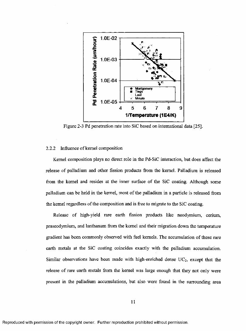
1.0E-02
1.0E-03
1 1.0E-04
g 1.0E-05
1/Temperature (1E4/K)
Figure 2-3 Pd penetration rate into SiC based on intemational data [25].
2.2.2 Influence of kernel composition
Kemel composition plays no direct role in the Pd-SiC interaction, but does affect the
release of palladium and other fission products from the kemel. Palladium is released
from the kemel and resides at the inner surface of the SiC coating. Although some
palladium can be held in the kemel, most of the palladium in a particle is released from
the kemel regardless of the composition and is free to migrate to the SiC coating.
Release of high-yield rare earth flssion products like neodymium, cerium,
praseodymium, and lanthanum from the kemel and their migration down the temperature
gradient has been commonly observed with fuel kemels. The accumulation of these rare
earth metals at the SiC coating coincides exactly with the palladium accumulation.
Similar observations have been made with high-enriched dense UC2 , except that the
release of rare earth metals from the kemel was large enough that they not only were
present in the palladium accumulations, but also were found in the surrounding area
11
Reproduced with permission of the copyright owner. Further reproduction prohibited without permission.

adjacent to the SiC coating. Thus, although the kemel composition has little effect on the
release of palladium, it does affect the release of the rare earth fission products [8].
2.2.3 Concentration dependence
The amount of palladium in a coated particle is a function of
1. heavy-metal humup and palladium fission yield
2. kemel density
3. kemel volume
The fission yield of palladium isotopes varies considerably with the fissile species
and is the largest single factor affecting the amount of palladium per particle. Thus, in
particles with a high percentage of plutonium isotopes (LEU and plutonium fuels) instead
of by or the palladium generation rate per particle will be higher for
comparable heavy-metal bumups. The concem over Pd-SiC interactions is greatest for
coated-particle fuels having low enrichments of Also, no threshold amount of
palladium per particle is necessary before penetration occurs [8].
The palladium accumulates in distinct “nodules”, so that even with low amounts of
palladium per particle, the concentration is high enough in localized areas to cause
corrosion. Thereby the amount of Pd per particle only affects the number of nodules
formed at the SiC coating [8].
2.2.4 Behavior in conjunction with rare earth fission products
As mentioned previously, the rare earth and palladium accumulations coincide with
each other at the inner surface of the SiC coating for particles with fuel kemels. Also they
are associated with each other during the penetration of the SiC coating.
The different sets of data observed are
1. rare earth and palladium penetration rates at temperatures > 1300°C [26]
12
Reproduced with permission of the copyright owner. Further reproduction prohibited without permission.

2. rare earth with no palladium penetration at temperatures > 1300°C [27]
3. palladium with no rare earth penetration at temperatures < 1400°C ([8], see
Figure 2-4)
These data suggest that at temperatures below 1400°C, palladium penetrates the SiC
at rates faster than rare earths, but that at temperatures above 1400°C, the reverse is true.
Because the average temperatures in a nuclear reactor are designed to be much less than
1400°C, palladium is the more important species for further study.
2.2.5 Influence of the SiC properties
The microstructure of the SiC layer affects the rate of palladium penetration, but the
exact correlation between microstructural features and penetration rate is still unknown.
Furthermore, it can be expected that the various surface reconstructions of SiC (discussed
above) will have a significant impact on the Pd/SiC interface formation and the Pd
penetration. Because the results of forming Pd/SiC interfaces with various SiC surface
structures are encouraging for limiting palladium penetration, efforts are in progress to
carefully examine SiC microstructures and their ability to suppress the corrosion caused
by palladium [8]. Within our project and based on the results presented in this thesis,
surface modification schemes to limit the chemical interaction between Pd and SiC will
be tested.
13
Reproduced with permission of the copyright owner. Further reproduction prohibited without permission.

<(Czot—<1ChUJZLU
1155“C
S- 10 û<j<0 .
t—O3ÛOcec_Zg5wIL ,
:6'. :<ô 1 0
S ic COATING RATE (jum/h)
Figure 2-4 Pd penetration rate into SiC as a function of SiC coating rate [8].
14
Reproduced with permission of the copyright owner. Further reproduction prohibited without permission.

CHAPTER 3
EXPERIMENTAL
Spectroscopic measurements are powerful tools in modem physics, and the
interaction between light and matter is one of the primary experimental areas for probing
the properties o f solids. Especially important for studying electronic properties is light in
the range of soft X-rays and the vacuum ultraviolet, which interacts with electrons in
solids. Techniques such as photoelectron spectroscopy and X-ray emission spectroscopy
are now standard tools for studying the electronic stmcture of materials [28]. In the
present thesis, we use X-ray photoelectron spectroscopy (XPS) and UV photoelectron
spectroscopy (UPS) to elucidate the electronic and chemical structure of the Pd/SiC
interface.
3.1 Measuring methods
Applying soft X-ray spectroscopies to the study of surfaces and interfaces has been
one of the prominent fields of Surface Science [29]. Photoelectron spectroscopy (PES), in
particular, has become the standard method to study the chemical and element-specific
properties of surfaces and interfaces [30]. As shown in Figure 3-1, PES involves the
ionization of a valence or core level and the subsequent detection of the emitted electron
w.r.t. its kinetic energy. The short inelastic mean free path of the emitted electrons makes
PES a very surface-sensitive method [29].
15
Reproduced with permission of the copyright owner. Further reproduction prohibited without permission.

Photoelectron Spectroscopy (RES)
Auger-ElectronSpectroscopy (AES)
Excitation
Conduction bandeither / or
Vaience band #X-ray Emission
Spectroscopy (XES)
Core level
Figure 3-1 Schematic diagram of core-level ionization (photoemission) in a
semiconductor. The two competing secondary processes for filling the core hole (Auger-
electron and X-ray emission) are also sketched. Solid arrows correspond to electrons,
dashed arrows to photons [29].
A hole in an ionized core level is filled by a weak bound electron. As shown in the
Figure 3-1, there are two ways to conserve energy in the process of filling the core hole;
either by emission of an Auger electron (Auger electron spectroscopy, AES) or by
emission of a fluorescence photon (X-ray emission spectroscopy, XES). While the former
is also a surface-sensitive probe due to the detection of electrons, the latter is a photon-in
photon-out technique which lends itself to study the surface near bulk and buried
interfaces [29].
16
Reproduced with permission of the copyright owner. Further reproduction prohibited without permission.

3.1.1 X-ray Photoelectron Spectroscopy (XPS)
XPS is highly surface-sensitive due to the short inelastic mean free path of
photoelectrons that are emitted from the solid. For XPS, A1 (1486.6 eV) or Mg K«
(1253.6 eV) are the common photon energies of choice in a lab environment. XPS, also
called “Electron Spectroscopy for Chemical Analysis” (ESCA), is an electron
spectroscopic method which uses X-rays to knock electrons out of inner-shell orbitals.
The kinetic energy (Ekin) of these photoelectrons is determined by the energy of the X-ray
radiation (hu) and the electron binding energy (Ebm) as given by:
Ekin = hu - Ebin (work function neglected) [31] .............. (1)
The energy of the photoelectrons leaving the sample is determined using a Concentric
Hemispherical Analyzer (CHA). This gives a spectrum with a series of photoelectron
peaks, as the example in Figure 3-2 illustrate. The figure shown is the survey spectrum of
an as-introduced SiC sample surface. Thereby the binding energy scale was calculated
according to equation (1) with hu (Mg Ka) = 1253.6 eV. The binding energies o f the
peaks are characteristic for each element. For example, as the C Is electrons have the
binding energy of 280 eV, one can see a peak at that particular binding energy in the
figure. The peak areas can be used to determine the composition of the material surface.
The shape of each peak and its binding energy can be influenced by the chemical state of
the emitting atom. Hence, XPS can provide chemical bonding information as well. XPS
must be carried out under ultra-high vaeuum (UHV) conditions.
17
Reproduced with permission of the copyright owner. Further reproduction prohibited without permission.

(Sic Survey Spectrum)80000
Mg XPS SiC-6H(0001)
(OKJ C 1s
C I s60000
■tI
O Is( O K )
c Q K WSi 2p40000
Si 2s
20000
01000 800 600 400 200
Binding Energy (eV)
Figure 3-2 SiC survey spectrum.
The impurity, oxygen present on the anodes of the X-ray source (explained later) also
takes part in the excitation of the sample. As a result, the peaks (e.g., C Is, Si 2s, and Si
2p) below the excitation energy of oxygen (543 eV) show up once again in the survey
spectrum, represented as O Ka in the above spectrum. Those peaks appear at a binding
energy which is higher than its true one by the difference of the photon energies of Mg
Ka and O Ka.
3.1.2 Ultraviolet Photoelectron Spectroscopy (UPS)
Ultraviolet light is shone at the sample using a Helium lamp emitting at 21.2 eV (He I
radiation) or 40.8 eV (He II radiation). The low photon energy in UPS means that deep
core electron levels can not be excited and only photoelectrons emitted from the valence
band or shallow core levels are accessible [32]. However, due to the lower inherent line
width, the spectral resolution for UPS is much higher than for XPS. UPS can also be used
18
Reproduced with permission of the copyright owner. Further reproduction prohibited without permission.

to identify molecular species on surfaces by analyzing the valence bonds of the
molecules. Angle-resolved UPS can be used to determine the band structure of the
material under investigation. Furthermore, the secondary electron cutoff in UPS spectra
can be used to determine the work function.
3.1.3 Auger-Electron Spectroscopy (AES)
As said before. X-rays can knock electrons out of inner-shell orbitals in an atom.
These excitations cause core electrons from atoms contained in the sample to be ejected,
resulting in a photoelectron and an atom with a core hole. The atom then relaxes via
electrons with a lower binding energy relaxing into the core hole. The energy thus
released can be converted into an X-ray or used to emit an additional electron. This
electron is called an Auger electron. After the emission of the Auger electron, the atom is
left in a doubly ionized state. The energy of the Auger electron is characteristic of the
element that emitted it, and can thus be used to identify the element. Furthermore, it gives
information about the local chemical structure o f the emitting atom. As in the case of
XPS, the short inelastic mean free path of Auger electrons in solids ensures the surface
sensitivity of AES [32].
3.2 Instrumentation
The apparatus at UNLV, shown in Figure 3-3, mainly consists of four connected UHV
chambers, namely an analysis chamber, a preparation chamber, a distribution chamber,
and an ECR plasma etching chamber. For the work in this thesis, only the first two
chambers are considered here.
19
Reproduced with permission of the copyright owner. Further reproduction prohibited without permission.

Figure 3-3 Picture of the ESCA in the Chemistry Dept., UNLV
The analysis chamber contains the X-ray source, UV source, sample manipulator, and
a concentric hemispherical analyzer (CHA), which will be discussed in detail below. The
preparation chamber is the chamber where the sample surface can be cleaned and/or
modified by sputtering and annealing. Also, metal evaporation onto the sample can be
done here. It is the intermediate chamber that the sample passes while transferring from
the loadlock (the chamber from where the sample can be introduced into the system) to
the analysis chamber.
3.2.1 Ultra High Vacuum (UHV)
UHV conditions are generally regarded as being in the region below ICf* mbar
(-750 pTorr). UHV is needed for surface science experiments as molecules in the
ambient will adsorb on a surface and change its properties. At a pressure of Iff* mbar, for
example, a monolayer of gas molecules will form on the surface in about 1 second
(assuming that every molecule to strike the surface sticks to the surface) [31]. This is
20
Reproduced with permission of the copyright owner. Further reproduction prohibited without permission.
clearly not enough time to do an experiment. However, at UHV pressures, which are a
factor 1000 and more lower in pressure, several hours of experiments can be performed
before the sample surface is significantly degraded.
In order to achieve UHV, some special procedures are needed. Initially, the vacuum
chamber is pumped down to 10' mbar using a rotary pump. Then, the chamber is
pumped down to about 10'^ mbar using oil diffusion pumps. At this stage, the vacuum
chamber is enclosed in an insulated tent and “baked” to a temperature of about 150“
Celsius for 24 - 48 hours. After cool down to room temperature, the chamber should
have a pressure in the UHV region. The process of baking removes residual molecules, in
particular water, which are adsorbed on the inside chamber walls. These molecules
slowly desorb from the chamber wall surfaces, and if the chamber was not baked, several
months would have to pass before the chamber achieves UHV conditions.
3.2.2 Sample Handling
Sample introduction into the analysis chamber is done by a series of successive
transfers. The sample sits on a metal stub which is placed at atmospheric pressure onto a
holder on a trolley in a loadlock chamber. Following evacuation, the sample is
transferred, first from the loadlock to the preparation chamber, and then from the latter
into the analysis chamber with the help of a moving cart. This is achieved by a sequence
of openings and closings of intervening gate valves, and of mechanical transfers from one
trolley to another and then onto the sample manipulator. The transfer is carried out with
bellows-sealed stub grips called ‘wobblesticks’. The highly flexible bellows allow a large
amount of both angular motion and axial translation motion of the central shaft, although
not, of course, rotational motion. A spring clip on the fork grips the sample stub firmly.
21
Reproduced with permission of the copyright owner. Further reproduction prohibited without permission.

Once the sample is transferred into the analysis chamber, it needs to be positioned
accurately for analysis by means of a manipulator. It provides X and Y lateral motions of
+/- 12.5 nun and a Z translation motion of 50 mm. These motions are possible via a
highly flexible all-welded bellows welded to the flange by which the manipulator is fitted
to the system. Axial rotation through the full 360° is driven through an offset knuckle
joint, also operating through a flexible bellow. Another option available is tilt, which
alters the angle o f the shaft inside the driving head [31].
3.2.3 Sample treatment
Because photoelectron spectroscopy, as mentioned above, is a surface-sensitive
probe, it is important to have well-defined and clean surfaces throughout an experimental
series. Surface cleanliness can be judged only by the techniques available in the analysis
chamber, in our case in particular by monitoring the intensity of oxygen-related signals.
Heating alone will produce clean surfaces on a few materials but is in general
inadequate unless used in association with a second technique. The problem is that the
balance between desorption from and segregation of impurities to the surface in certain
temperature ranges is characteristic of the material and of the impurity. The segregating
contaminants must therefore be removed in some other way, and by far the most
universally used method of doing that is by noble gas ion bombardment (“sputtering”).
Ions, usually of argon, with energies chosen between 50 eV and 5 keV, are directed at the
surface. Energy is exchanged with atoms in and near the surface as a result of successive
collisions between the incident ions and the sample atoms in rest positions, as well as
involving displaced atoms with excess energy, resulting in a cascade process that causes
ejection of atoms and clusters from the surface. The surface is therefore eroded by loss of
22
Reproduced with permission of the copyright owner. Further reproduction prohibited without permission.

material, the process of erosion being termed “sputtering”. In sputtering, the ions are
produced in and directed and focused by an ion gun.
The best method of preparing a clean surface is a series of consecutive heating and
ion bombardment steps, so that contaminants segregating or adsorbing to the surface in a
heating cycle are removed in a bombardment cycle. The process has to be continued for
as many cycles as are necessary either to remove all contaminants from the sample
completely or, if that is not practical, to remove them from a certain depth in the sample
by a careful choice of temperature and of bombardment conditions. Likewise, the
annealing step will minimize the structural surface damage inflicted by the sputtering
cycle, as can be monitored by techniques that are sensitive to surface structure (eig., Low-
Energy Electron Diffraction - LEED).
3.2.4 X-Ray Source
The interaction of a photon with a core level electron is given by [31],
Ek = hv-Eb-eO
where
Ek = kinetic energy of ejected photoelectron w.r.t. the vacuum level
hv = characteristic energy of X-ray photon
Eb = binding energy of the core level w.r.t. the Fermi level
e 0 = work function term
From the above equation, it is evident that the line width of Ek will depend on the line
width of hv. Furthermore, the lifetime broadening of the core level plays an important
role (a so-called “final state effect”) via Heisenberg’s uncertainty principle. In XPS,
chemical information is extracted by a detailed analysis of individual elemental spectra,
including resolution of contributions from the various chemical states present, from
23
Reproduced with permission of the copyright owner. Further reproduction prohibited without permission.

which it follows that the best energy resolution should be used compatible with the
signal-to-noise ratio in the particular spectrum.
Generally, X-rays are generated in a material by bombardment with electrons of
sufficient energy. For a particular X-ray line, photon emission starts at the ionization
threshold of the core level involved and increases rapidly as the electron energy is
increased, eventually saturating at some energy much higher than the threshold. For
optimum sensitivity in analysis at a chosen energy resolution, the photon flux on the
sample surface should be maximized; since the flux is directly proportional to the
electron current bombarding the anode, as high a bombarding current should be used as
the source will withstand (in our case, the X-ray source can be operated at up to 300 W
for Mg Ka and 600 W for A1 Ka). Since the flux irradiating the sample varies inversely as
the square of the distance from the anode to the sample surface, it is essential to place the
sample as close to the anode as all other constraints will permit.
In our experimental setup, the end of the copper anode has two angled faces, on one
of which a film of aluminum is deposited and on the other a film of magnesium. There
are two filaments, one for each anode material. Each filament and the surrounding shields
are at ground potential, and a high accelerating potential of up to +15 kV is applied to the
anode. With careful design of shields and of positioning of the semi-circular filaments,
electrons from each filament bombard only the anode face nearer to it. X-rays generated
in the bombarded face then pass out through an aperture in the surrounding cylindrical
shield, covered with a thin sheet of aluminum foil. The aluminum foil is necessary in
order to screen the sample from stray electrons, heating effects and any contamination
originating in the source. Switching from Mg Ka to A1 Ka radiation and back again is
24
Reproduced with permission of the copyright owner. Further reproduction prohibited without permission.

simple and can be done in a couple of minutes. With possible maximum power
dissipation up to 600 W and with such a compact design, heat must be removed from the
anode quickly and efficiently, which necessitates a forced flow of water at high pressure
[31].
3.2.5 Concentric Hemispherical Analyzer (CHA)
The CHA consists of two metal hemispheres (Figure 3-4). One hemisphere is being
shaped concave, and the other convex. They are arranged such that their centers of
curvature are coincident. Different voltages are placed on each hemisphere such that
there is an electric field between the two hemispheres. Electrons are injected into the gap
between the hemispheres. If the electrons are traveling very fast, they will impinge on the
outer hemisphere. If they are traveling very slowly, they will be attracted to the inner
hemisphere. Hence only electrons in a narrow energy region (called the pass energy)
succeed in getting all the way through the hemispheres to the detector. A series of lenses
are placed before the CHA. The lenses enable two operating modes - Constant Retard
Ration (CRR), or Constant Analyzer Energy (CAE). In the CRR mode, the electrons are
slowed down by an amount which gives a constant ratio of the electron energy to be
analyzed. That is, if the retard ratio is 10, and 1000 eV electrons are to be detected, then
the electrons will be decelerated to 100 eV, and the pass energy will be set to 100 eV. In
the CAE mode, the pass energy is fixed. Hence if the pass energy is 50 eV, then electrons
of 1000 eV will have to be retarded by 950 eV in order to be detected. The CRR mode
gives constant resolving power and the CAE mode gives constant energy resolution. For
our XPS spectra, we have consistently used the CAE mode [31].
25
Reproduced with permission of the copyright owner. Further reproduction prohibited without permission.

c o n c e n tr ic h e m is p h e r e s
e le c tro n p a th
sa m p le
Figure 3-4 Concentric Hemispherical Analyzer (CHA) [32].
3.2.6 Electron detector
Multi-channel plate electron multipliers are used to count the individual electrons
arriving at the detector. These consist of a three chevron-mounted plates with 256x256
channels, through which an incoming electron pulse is amplified by using an overall
acceleration voltage of 4 kV. A resistive anode set-up allows the detection of the local
position of the electron pulse, and a custom-written software integrates over this two-
dimensional intensity image, taking the shape of the iso-energy surface into account. The
output of the software is thus a spectrum of intensity vs. kinetic energy [33].
3.2.7 E-beam metal evaporator
The metal evaporator is an evaporator for small and medium quantities of many
materials in the temperature range of 400K to 3100K. E-beam evaporation uses an
electron beam to heat a source. Electrons are generated with a heated filament and are
accelerated by several kV. The electron current is small, typically around 100 mA. The
26
Reproduced with permission of the copyright owner. Further reproduction prohibited without permission.

material for evaporation is either placed in a crucible or evaporated directly from a wire
of the desired material (as was done in our case of Pd). An integrated flux monitor allows
an in-situ deposition control. Water-cooling ensures negligible outgassing during
operation.
A sketch of the metal evaporator and its components is shown in Figure 3-5:
Rotary driv#50mm ttiimbte
203
2 75" {MW35CF) Mounting flange
200
Fhjx mon Nor Shytter __
Figure 3-5 The e-beam metal evaporator and its various parts [34].
27
Reproduced with permission of the copyright owner. Further reproduction prohibited without permission.

CHAPTER 4
RESULTS AND DISCUSSIONS
Three experimental series of Pd/6H-SiC(0001) interfaces were prepared under
controlled conditions in an ultra-high vacuum environment and studied using XPS and
UPS, respectively. In the first experimental series, the formation of the interface between
a thin film of evaporated Pd and a well-ordered single crystal 6H-SiC(0001) surface at
room temperature was investigated (Si-terminated 6H-SiC(0001) single crystals were
purchased from Mateck, Jiilich, Germany). In order to gain more directly applicable
information about SiC layers in TRISO particles, two other experimental series (series 2
and series 3) were prepared. In these series, the SiC surface was cleaned and structurally
disordered by extensive Ar^-ion sputtering with 2 keV ions in order to mimic the fact that
TRISO SiC layers are not single-crystalline. The Pd layer thickness was then
successively increased, and each step monitored by XPS and UPS. For series 2, the
sample was kept at room temperature during deposition, whereas for series 3, it was
heated to the currently highest attainable sample temperature in our system (approx. 800°
C).
28
Reproduced with permission of the copyright owner. Further reproduction prohibited without permission.

4.1 Experimental series 1
The survey spectrum of an as introduced SiC of this series is shown in Figure 4-1.
Being an uncleaned sample, many adsorbates were present on the SiC surface (0 1s and
F Is). Since the sample was smaller than the probing area o f the electron analyzer, also
Ta signals can be found (Ta was used to fix and contact the sample). The peaks measured
with O Ka are due to oxygen contaminations on the X-ray anode resulting in an O Kg line
in the excitation spectrum. The Auger peaks, O KVV, F KLL, and C KVV can also be
seen.
(Survey Spectrum of Series 1)
90000
C K WO 1s
> 60000
Ta 4a
30000 Ta 4f-
MgK^XPS6H-SiC(0001)
1000 800 600 400 200 0
Binding Energy(eV)
Figure 4-1 Survey spectrum of the as-introduced SiC sample of series 1.
In contrast to the two experimental series discussed below, the 6H-SiC(0001) single
crystal surface was now prepared to regain its single-crystalline structure and a high
degree of lateral order at the surface, as evidenced by low-energy electron diffraction
29
Reproduced with permission of the copyright owner. Further reproduction prohibited without permission.

(LEED). This was done by various sputtering and annealing steps. After the single
crystalline surface was prepared, a thin layer of Pd was deposited on SiC and monitored
using XPS. A rough estimate based on the attenuation of the Si 2p signals suggest an
approximate thickness of a monolayer.
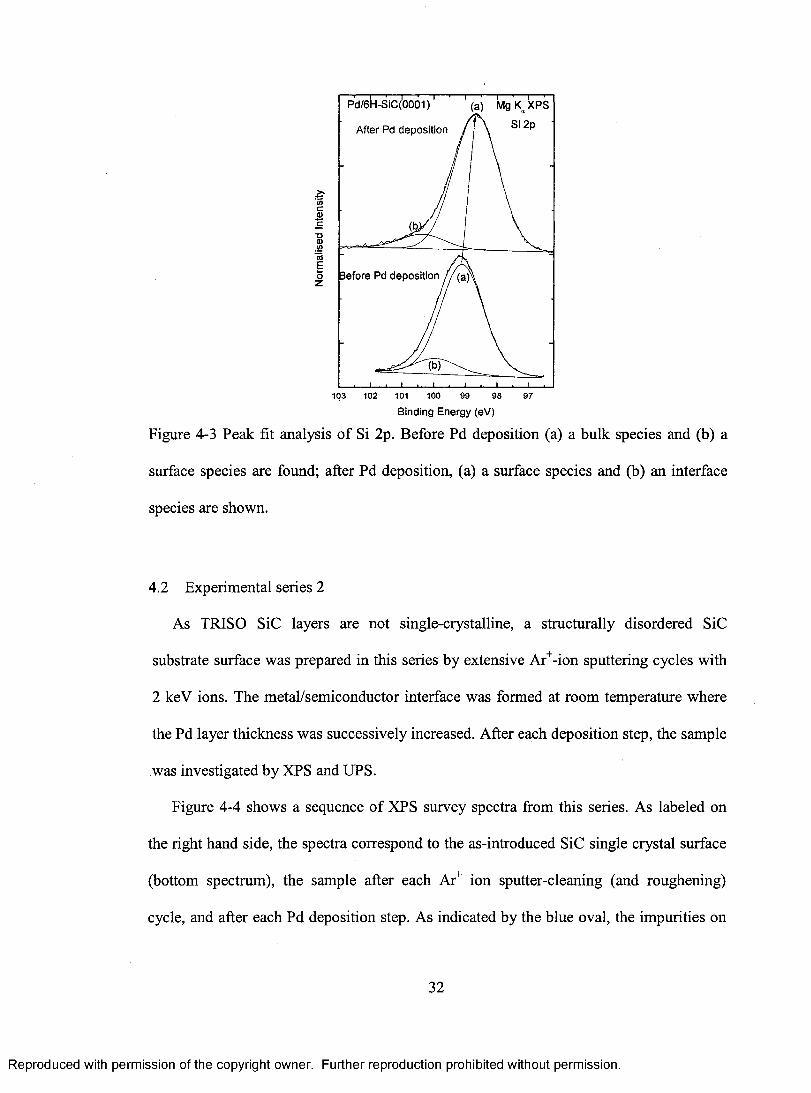
Figure 4-2 represents the C Is core level before and after the deposition of the thin Pd
layer. As can be seen from the included peak fit analysis using Voigt line shapes and a
linear background, two chemically different carbon species (282.8 eV, 284.3 eV) exist at
the clean and uncovered SiC(OOOl) surface, which we ascribe to a bulk (a) and a surface
species (b), respectively. After the Pd deposition, three different carbon species (282.4
eV, 284.0 eV, and 286.0 eV) exist which are ascribed to (a) a bulk species, (b) an
interface species, and (c) a reacted species. The latter is possibly due to a difftision of Pd
into the region near the interface (and presumably fiirther into the bulk of SiC). In
parallel, the Si 2p core levels (shown in Figure 4-3) also show the existence of two
different Si species, both before and after the interface formation. Again, these are
ascribed to a surface and a bulk component before formation of the interface and to an
interface and a bulk component after Pd deposition.
30
Reproduced with permission of the copyright owner. Further reproduction prohibited without permission.

Pd/6H-SiC(0001) .After Pd deposition/
Mg XPS
C IS ■
■a
Before Pd deposition
287 286 285 284 283 282 281 280
Binding Energy (eV)
Figure 4-2 Peak fit analysis of the C Is peaks before and after Pd deposition on 6H-
SiC(OOOl). The C Is Species shown are (a) a bulk species, (b) a surface species before Pd
deposition and (a) a bulk species, (b) an interface species, and (c) a reacted species after
Pd deposition.
In both cases, there is an upward shift (i.e., to lower binding energies) of all electronic
levels, as indicated by the arrows in Figures 4-2 and 4-3. This is presumably due to a
change in surface band bending of the SiC substrate upon formation of the
metal/semiconductor interface.
31
Reproduced with permission of the copyright owner. Further reproduction prohibited without permission.
Pd/6H-SiC(0001) (a) Mg XPS
T \ Si 2pAfter Pd deposition
tC0c
iBefore Pd deposition / / ( a yoz
102 101 100 99 98103 97
Binding Energy (eV)
Figure 4-3 Peak fit analysis of Si 2p. Before Pd deposition (a) a bulk species and (b) a
surface species are found; after Pd deposition, (a) a surface species and (b) an interface
species are shown.
4.2 Experimental series 2
As TRISO SiC layers are not single-crystalline, a structurally disordered SiC
substrate surface was prepared in this series by extensive Ar^-ion sputtering cycles with
2 keV ions. The metal/semiconductor interface was formed at room temperature where
the Pd layer thickness was successively increased. After each deposition step, the sample
was investigated by XPS and UPS.
Figure 4-4 shows a sequence of XPS survey spectra from this series. As labeled on
the right hand side, the spectra correspond to the as-introduced SiC single crystal surface
(bottom spectrum), the sample after each Ar^ ion sputter-cleaning (and roughening)
cycle, and after each Pd deposition step. As indicated by the blue oval, the impurities on
32
Reproduced with permission of the copyright owner. Further reproduction prohibited without permission.
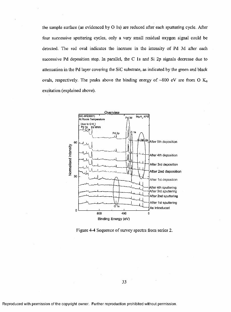
the sample surface (as evidenced by O Is) are reduced after each sputtering cycle. After
four successive sputtering cycles, only a very small residual oxygen signal could be
detected. The red oval indicates the increase in the intensity of Pd 3d after each
successive Pd deposition step. In parallel, the C Is and Si 2p signals decrease due to
attenuation in the Pd layer covering the SiC substrate, as indicated by the green and black
ovals, respectively. The peaks above the binding energy of -800 eV are from O IQ
excitation (explained above).
SiC-6hl(0001) r At Room Temperature
[due to O KJ Pd 3p Pd“MNN
O verv iewPri3d Mg K XPS
gI■oI(0E
C 1s ^\ f \
A
800 400
Binding E n erg y (eV)
After 5th deposition
After 4th deposition
After 3rd deposition
A fter 2 n d d ep o sitio n
After 1st deposition
After 4th sputtering After 3rd sputteringAfter 2nd sputtering
After 1st sputtering
As introduced
Figure 4-4 Sequence of survey spectra fi'om series 2.
33
Reproduced with permission of the copyright owner. Further reproduction prohibited without permission.
Pd-deposition @ room tem pe-ature
90
After 5th deposition
After 4th deposition
I After 3rd deposition0)c 60
1 After 2nd deposition
After 1st depositionIAfter 4th sputter
After 3rd sputter30
After 2nd sputter
After 1st sputter
As Introduced286 284 282 280 278
Binding Energy (eV)
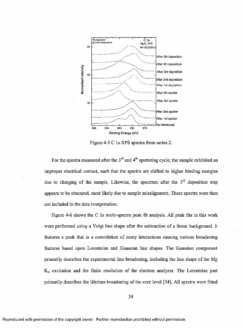
Figure 4-5 C Is XPS spectra from series 2.
For the spectra measured after the 3' ' and 4* sputtering cycle, the sample exhibited an
improper electrical contact, such that the spectra are shifted to higher binding energies
due to charging of the sample. Likewise, the spectrum after the 3' '* deposition step
appears to be obscured, most likely due to sample misalignment. These spectra were then
not included in the data interpretation.
Figure 4-6 shows the C Is multi-spectra peak fit analysis. All peak fits in this work
were performed using a Voigt line shape after the subtraction of a linear background. It
features a peak that is a convolution of many interactions causing various broadening
features based upon Lorentzian and Gaussian line shapes. The Gaussian component
primarily describes the experimental line broadening, including the line shape of the Mg
Kot excitation and the finite resolution of the electron analyzer. The Lorentzian part
primarily describes the lifetime-broadening of the core level [34]. All spectra were fitted
34
Reproduced with permission of the copyright owner. Further reproduction prohibited without permission.

simultaneously to be able to set common parameters between the different fits, in
particular to obtain the same separation between the different species, the same line
width, etc. This ensures that quantitative information about the emergence of new
chemical species can be obtained.
IÎO
SiC-dH(OOOI) ' Pd-deposition @ room temperature
C Is Mg K XPS
5th deposition
60 4th deposition
2nd deposition
1st deposition
30 4th sputter
2nd sputter
1st sputter286 284 282 280 278
Binding Energy (eV)
Figure 4-6 Peak fit analysis of the C Is spectra.
As can be seen from the included peak fit analysis, three chemically different carbon
species exist at the clean and uncovered SiC(OOOl) surface, and their intensity varies as a
function of Pd deposition. The three carbon species are (a) a bulk species (at 279.5 eV in
the topmost spectrum), as this peak is decreasing gradually in intensity after each Pd
deposition step, (b) an interface species (at 280.8 eV in the topmost spectrum), as this
peak is gradually intensified as a function of deposition, and (c) presumably adventitious
carbon. The interface species (b) gets more prominent than the surface species (a) as a
35
Reproduced with permission of the copyright owner. Further reproduction prohibited without permission.

function of Pd coverage. There is also a shift of species (a) and (b) towards smaller
binding energies (indicated by the arrows in Fig. 4-6), most likely due to a long-range
charge transfer (as is commonly found in the formation of Schottky contacts [38]), which
indicates a change in surface band bending of the SiC substrate due to the formation of
the metal/semiconductor interface (explained later).
The relative changes in the areas of the three C Is species are shown in Figure 4-7.
After depositing Pd, one can see a gradual decrease in the area of the C Is surface species
(a), while the areas of the two other peaks increase. This points towards an intermixing at
the Pd/SiC interface.
C 1sMg K XPS ■
6H-SiC(0001)- Pd-deposition . @ room temp.
peak (a)
< 4 0
3 0peak (b)
20
peak (c)
4th 4th1st2nd 2nd3rd 5th1stsputter sputter sputter sputter deposition deposition deposition deposition
Figure 4-7 Area percentages o f all three C Is species of the second series.
36
Reproduced with permission of the copyright owner. Further reproduction prohibited without permission.

Similarly, the Si 2p spectra of this series (shown in Figure 4-8) change significantly
as a function of sample treatment. As in the carbon spectra, there is an emergence of an
additional silicon structure after deposition (indicated by the oval).
Si 2pS i C . 6 H ( o b o i ) 'At Room Temperature
Mg XPS
After 5th deposition
60After 4tti deposition
After 2nd depositionT3
After 1st deposition
After 4th sputter30
After 2nd sputter
As Introducedtoo 98 96 94
Binding Energy (eV)
Figure 4-8 Si 2p XPS spectra, second series.
Figure 4-9 shows the peak fit of the Si 2p XPS spectra, which again were fitted
simultaneously. Here in this work, for Si 2p, the fits are done by taking the spin-orbit
splitting of the Si 2p levels into account. That is, for each species, a doublet (consisting of
the Si 2pi/2 and 2p3/2 levels) was fitted with constant area ratio (1:2) and constant
separation (2.24 eV). As in the case of the C Is spectra, the spectra after the 3 ' and 4'*’
sputter step are shifted due to charging problems. As can be seen from the included peak
fit analysis, the clean and uncovered SiC(OOOl) surface can be well described by a single
peak duplet. To optimize the fit, a second (weak) species was included at approx. 100 eV.
37
Reproduced with permission of the copyright owner. Further reproduction prohibited without permission.

The main peak is associated with the bulk species, while the weak shoulder can be
attributed to some residual Si-0 bonds, which is corroborated by peak (b) in the fit
analysis of the earlier sputter steps (i.e., with a larger amount of residual O contamination
at the surface). After Pd deposition, two species are clearly required to satisfactorily
describe the spectra. They are ascribed to a SiC bulk species (a) and an interface species
(c), as the interface species increases with increasing Pd coverage (which can be seen
quantitatively in Figure 4-10). An alternative interpretation of the structure (c) could be
based on an extrinsic (correlated) energy loss of the outgoing photoelectrons while
passing through the Pd layer. There is a shift of species (a) towards smaller binding
energies in a similar manner as seen in the C Is spectra, which indicates a change in
surface band bending of the SiC substrate due to the formation of the
metal/semiconductor interface.
Pd-deposition @ room temp. Mg XPS
6H-SiC(0001)
5th deposition
4th deposition60
</)c& 2nd depositionc
Î(0 1st depositionoz
30 4th Sputter
2nd Sputter
As Introduced100 96102 98 94
Binding Energy (eV)
Figure 4-9 Peak fit analysis of the Si 2p spectra, second series.
38
Reproduced with permission of the copyright owner. Further reproduction prohibited without permission.

The change in the area percentages of the Si 2p species is shown in Figure 4-10. After
depositing Pd, there is a gradual decrease in the area of the bulk species (a) and an
increase of the intensity of the interface species (or loss feature) (c).
Pd-deposition @ room temp. Si 2p Mg K XPS
6H-SiC(0001)peak (a)'
40ÿ.<30
peak (b)
peak (c)
AsIntroduced 4th 2nd
sputter sputter sputter ^®POsition deposit^n deposition depositiondeposition3rd 4th2nd 5th
Figure 4-10 Percent area plot of the Si 2p species
Figure 4-11 shows the Pd 3d3/2 spectra as a function of deposition steps. After each
deposition, the Pd Sdg/z signal increases. Furthermore, the peak line shape is gradually
getting asymmetric, as shown in Figure 4-12 by comparing the spectra from the thinnest
and thickest Pd film. This asymmetry is ascribed to the increasingly metallic character of
the overlayer (explained below).
39
Reproduced with permission of the copyright owner. Further reproduction prohibited without permission.

I
1z?g
I
Pd-deposition @ room temp.
Pd3d,, ■ Mg K XPS 6H-SiC(0001)
6
5th deposition
4th deposition
3
3rd deposition
2nd deposition
1st deposition
339 336342Binding Energy (eV)
Figure 4-11 Pd 3Ü3/2 spectra as a function of deposition step
(/>c0)
Pd3d,Pd-deposition @ room temp.
3/2
40
thin Pd film
36th ic k P d fiim
32342 340 338346 344
Binding Energy (eV)
Figure 4-12 Comparison of Pd 3d3/2 peaks for the thickest and thinnest Pd film.
40
Reproduced with permission of the copyright owner. Further reproduction prohibited without permission.

The arrow indicates the region of increased asymmetry of the lineshape for the
thickest film, corresponding to an increased metallicity of the overlayer.
After the 1 ‘ deposition, only a thin layer of Pd is deposited and it may be deposited as
individual islands on the surface. If this is the case, Pd atoms may be present in several
different environments (such as Pd bonded to the SiC substrate, Pd with one Pd neighbor,
with two Pd neighbors, etc.). Due to the large number of different environments in this
case, the Pd Sds/z peak after the 1®‘ deposition (thin Pd film) is broader than the peak after
the 5* deposition (thick Pd film), as can be seen in Fig. 4-12. However, it is still
symmetric due to the lack of metallic character in the confined Pd islands. Only for the
thicker Pd films, the typical asymmetric line shape found for metals (Doniach-Sunjic) is
observed. This asymmetry is induced by the possibility of very small energy losses of the
outgoing photoeleetron due to scattering processes that promote electrons from just
below the Fermi energy to states just above the Fermi energy. Such losses give rise to a
continuous shoulder of metallic photoemission peaks, as observed here. The findings thus
indicate that the film is not yet metallic after the first deposition step (see also the
discussion of the UPS spectra below).
As can be seen in the quantitative summary of the peak shifts mentioned above in
Figure 4-13, the C, and Si levels are significantly pushed to lower binding energies after
the first deposition step, and then gradually shift to even lower binding energies as a
function of deposition. This indicates that there is a change in the band bending of SiC
during the interface formation, which will be discussed in more detail below.
Furthermore, we find a more pronounced decrease of the Pd Bda/a binding energy, which
41
Reproduced with permission of the copyright owner. Further reproduction prohibited without permission.

is associated with the gradual formation of metallic regions on the SiC surface and the
improved screening that is associated with larger metallic domains.
6H-SiC(0001) Pd-deposition @ room temp.
5thdepositior Pd3d 3/2
Si 2p /4thdeposition C Is
3rddeposition
2nddeposition
1stdeposition
4th sputter1.0 0.8 0.6 0.4 0.2 0.0 -0 .2 -0 .4 -0 .6 -0 .8 -1 .0 -1 .2 -1 .4 -1 .6 -1 .8 -2 .0 -2 .2
Energy Shift (eV)
Figure 4-13 Relative binding energy change in the peak positions of C Is, Si 2p, and Pd
3 da/2.
Figure 4-14 shows the UPS survey spectra which show the secondary electron cutoff
(SEC) region and the valence band (VB) region. The detailed SEC and the upper valence
band are shown in Figures 4-15 and 4-17, respectively.
42
Reproduced with permission of the copyright owner. Further reproduction prohibited without permission.

Overview Spectra90He I (UPS) SiC-6H(Q0Q1)
At Room Temperature80
After 5th deposition
After 4th deposition
After 3rd depositionc
15 40
After 2nd deposition
i After 1st depositionoz
After 4th sputter
After 3rd sputter
After 1st sputter
As Introduced20 3010
Kinetic Energy (eV)
Figure 4-14 Sequence of UPS survey spectra for the second series, taken with a bias
voltage of 15 V and not taking the work function of the electron analyzer into account.
From the SEC spectra, the work function of the sample at each step can be
determined by a linear extrapolation of the leading edge and by evaluating the intersect
with the baseline extrapolation. The derived values are shown in Figure 4-18 as a
function of sputter treatment and/or Pd deposition. The work function increases
gradually, indiacting that the overlayer converts gradually from isolated Pd islands to
metallic Pd areas. However, the absolute values found in our study are unexpectedly low,
both for SiC (literature value: 4.8 eV [35]) and metallic Pd (literature value: 5.1 eV [36]).
We suspect that this is due to a calibration problem. Nevertheless, relative changes are
estimated to be accurate within 0.2 eV.
43
Reproduced with permission of the copyright owner. Further reproduction prohibited without permission.

SEcutoff SpectraNe I (UPS)SiC-6H(0001)
At Room TemperatureAfter 5th deposition
After 4th deposition After 3rd deposition
60
(0c After 2nd depositionI
1at
After 1st deposition
After 4th sputter30
After 3rd sputter
After 1st sputter
As Introduced
14 16
Kinetic Energy (eV)
Figure 4-15 Secondary electron cut-off spectra of the second sample series.
Au VB Spectra
He I (UPS)
4000
0c
2000
3 2 1 0
Binding Energy (eV)
Figure 4-16 Au reference spectrum.
44
Reproduced with permission of the copyright owner. Further reproduction prohibited without permission.

VB SpectraHe I (UPS) SiC-6H(0001) Pd-deposition @ room temp.
I After 5th deposition After 4th deposition After 3rd deposition ^fter 2nd deposition
nsioz
After 1st deposition
lutter
After 1st sputter
As Introduced3 24 1 0
Binding E nergy (eV)
Figure 4-17 Upper valence band spectra o f the second sample series
From the spectra of the upper valence band, the valence band maximum (VBM) can
be determined by a linear extrapolation of the leading edge and by evaluating the
intersect with the baseline extrapolation. As a function of sputter treatment, the VBM
shifts upwards, i.e., to lower binding energies (as shown in figure 4-18). As the Pd
coverage increases, a Fermi edge emerges between 32.05 and 32.15 eV (the Fermi energy
is evaluated as the inflection point of the Fermi edge). The Fermi edge position of a Au
reference sample, which was observed at 32.20 eV. This indicates that the Pd film
increasingly gets a more “bulk-metallic” character throughout the deposition series.
45
Reproduced with permission of the copyright owner. Further reproduction prohibited without permission.

0.0
0.2
^ 0.4&- 0.6
0.8
1.2
6H-SIC(0001) • Pd-deposition - @ room temp. .
1st 4th 1st 2nd 3 ^ 4th 5thIntroduced sputter sputter deposition deposition d e p o s i to n deposition depositionAs
Figure 4-18 Position of the valence band maximum/Fermi edge for the second series.
Figure 4-19 is the plot of the work function of the sample at each step. As can be seen
from the figure, the work function of the sample is increasing as Pd deposition starts.
6H.SiC(0001)Pd-deposition @ room temp.4.4
4.2
4.0co
3.8Üc3u_
3.6
I 3.4
3.2
3.0
2.81 s t 3 rd 4 t(, 1 s t 2 n d 4 t t i 5 ttis p u t t e r s p u t t e r s p u t t e r d e p o s i t io n o e p o s i t io i‘?®P°®'‘'° 'ld e p o s l t io f ie p o s i t lo n
In tro d u c e d
Figure 4-19 Work Function plot of the sample.
46
Reproduced with permission of the copyright owner. Further reproduction prohibited without permission.

4.3 Experimental series 3
In order to make the investigation of the Pd/SiC-single crystal interface more directly
applicable to SiC layers in TRISO particles, the sample in this series was not only
structurally disordered by extensive Ar^-ion sputtering cycles with 2 keV ions, but the
metal/semiconductor interface was furthermore also formed at elevated temperatures
(approx. at 800°C, the currently highest attainable temperature in our system). As in the
previous series, the Pd layer thickness was successively increased.
Figure 4-20 shows a sequence of XPS survey spectra from this series. The sample
was cleaned before the Pd deposition by prolonged Ar^-sputtering, leading to an almost
complete removal of the O Is signal. As a function of deposition, we observe an increase
of the Pd signals as well as an attenuation of the Si and C signals.
IoZ
Overview■>— I— '—SIC-6H(0001)At High Temperature
Mg XPS
Pd3p
C IS S i2s Si2p
After 5th deposition60
After 4th deposition
After 3rd deposition
After 2nd deposition30
After 1st deposition0 1 s
After sputtering
As Introduced6001000 800 400 200 0
Binding Energy (eV)
Figure 4-20 Sequence of XPS survey spectra of series 3.
47
Reproduced with permission of the copyright owner. Further reproduction prohibited without permission.

Figure 4-21 shows a sequence of C Is XPS spectra, obtained from this series, i.e., the
interface sample grown at approx. 800°C substrate temperature. The spectra change
significantly as a function of sample treatment. During the sputter treatment, adventitious
carbon is removed, which can be seen by the absence of the peak at 282 eV in the
spectrum following the sputter-cleaning.
. P d - d e p o s i t i o n
@ 8 0 0 °CC 1s
M g K _ _ X P S
S i C - 6 H ( 0 0 0 1 )
After 5tti Deposition
After 4th Deposition4 0
After 3rd DepositionTO
After 2nd Deposition
After 1st Deposition
After 1st sputter
As introduced2 8 6 2 8 4 2 8 2 2 8 0 2 7 8 2 7 6 2 7 4
Binding Energy (eV)
Figure 4-21 Sequence of C Is XPS spectra.
During the Pd deposition, we find the emergence of an additional carbon species, as
indicated by the oval in the above figure. In the topmost spectrum, we find a strongly
different C Is peak shape. The multi-spectra peak fit of C Is is shown in Figure 4-22. At
least two chemically different carbon species exist at the clean and uncovered SiC(OOOl)
surface.
Upon deposition of Pd, two major effects are visible, first a shift of the main peaks
(indicated by the arrows) towards smaller binding energies, most likely due to a change
48
Reproduced with permission of the copyright owner. Further reproduction prohibited without permission.

in band bending, and second a variation in the relative intensities of the various C
species.
Ci sM g K _ _ X P S
6 H - S i C ( 0 0 0 1 )
Pd-deposition ■@ approx. 800 °C
5th deposition
I Wh deposition
c
.1 3rd deposition
Iz 2nd deposition20
1st deposition
after sputter
2 8 6 2 8 4 2 8 2 2 8 0 2 7 8 2 7 6
Binding Energy (eV)
Figure 4-22 Peak fit analysis of C Is spectra.
From the peak fit analysis, the three carbon species are ascribed to (a) a SiC bulk
species (at 279.1 eV in the topmost spectrum), (b) an interface species (at 280.3 eV in the
topmost spectrum), and (c) adventitious carbon. The species (a) is less dominant when
compared with the species (b) and (c) after the deposition of Pd.
The relative change in the areas of the three C Is species is shown in Figure 4-23. As
also observed from series 2, after depositing Pd, there is a gradual decrease in the relative
area of the bulk species of the C ls peak (a), whereas the relative areas of the other two
peaks increase. This supports the interpretation that the interface species (b) is
49
Reproduced with permission of the copyright owner. Further reproduction prohibited without permission.

dominating over the bulk species (a) after Pd deposition. This is most likely due to an
intermixing at the interface.
Pd-deposition @ 800°C80 C IS XPS - 6H-SiC(0001).peak (a)
70
60
50
40
30
peak (b)20
10peak (c)
0
3rddeposition
1stdeposition
2nddeposition
5thdeposition
4thdeposition
Aftersputter
Figure 4-23 Area percentages of all three species of Cls, third series.
Similarly, the sequence of Si 2p spectra is shown in Figure 4-24. As the thickness of
the Pd layer increases gradually, we find a shift of the Si 2p peak towards lower binding
energies, which can best be seen in the peak analysis of the Si 2p spectra in Figure 4-25.
There is an emergence of an additional Si 2p species after the deposition starts (indicated
by the oval).
50
Reproduced with permission of the copyright owner. Further reproduction prohibited without permission.

Si 2pMg XPS .^iC-6H(0001)
At High Temperature60
After 5th deposition
After 4tfi deposition40
After 3rd deposition
After 2nd deposition
After 1st deposition
After 1st sputter
As Introduced98 96 94 92100Binding Energy (eV)
Figure 4-24 Si 2p XPS spectra, third series.
As can be seen from the included peak fit analysis in Figure 4-25, two species, (a) a
bulk species and (b) a surface species, exist at the clean and uncovered SiC(OOOl)
surface. After the final deposition step, three species, (a) a surface species, (c) an
interface species, and (d) an additional species, which is interpreted as either an oxidized
Si species or a loss peak, can be seen. There is a shift of the main peaks towards smaller
binding energies in the similar manner as seen in C Is spectra, which indicates a change
in surface band bending of the SiC substrate due to the formation of this
metal/semiconductor interface.
51
Reproduced with permission of the copyright owner. Further reproduction prohibited without permission.

Si2pMg XPS 6H-SiC(0001)
Pd-deposition @ approx. 800 °C
5th deposition
4th deposition
I£ 3rd depositionc
Ig 30 2nd deposition
1st deposition
after sputter
As Introduced
100 98 96 94
Binding Energy (eV)
Figure 4-25 Peak fit analysis of the Si 2p spectra. Before Pd deposition, (a) bulk, (b)
surface species; and after Pd deposition, (a) surface, (c) interface species are seen. An
additional species (d) can also be seen after the last deposition step.
The relative change in the areas of the Si 2p species is shown in Figure 4-26. After
depositing Pd, there is a gradual decrease in the area of the bulk species (a) and an
increase in the intensity of the interface species (b). Figure 4-27 shows the Pd 3d3/2
spectra as a ftmction of deposition steps. After each deposition, the Pd 3d3/2 signal
increases. Gradually, the shoulder of the Pd 3d3/2 peak at higher binding energies
increases (shown by the oval), indicating that the peak is getting asymmetric, i.e., towards
a metallic line shape expected for bulk Pd.
52
Reproduced with permission of the copyright owner. Further reproduction prohibited without permission.

s
Pd-deposition @ 800°C Si 2p XPS 6H-SIC(0001)
70leak (a)
60
50
40
30
20
10peak (c)
p eak (b)
0
1st 3rd 4th2nd 5thAfterAsIntroduced sputter deposition deposition deposition deposition deposition
Figure 4-26 Percent area plot of Si 2p, third series.
. Pd-deposition @ approx. 800 °C ■
Mg XPS 6H-SiC(0001)
6
5th deposition4
T 3
4th deposition
O)
3rd deposition2
2nd deposition
1st deposition
342 340 338 336Binding E nergy (eV)
Figure 4-27 Pd hdyi spectra as a function of Pd deposition.
53
Reproduced with permission of the copyright owner. Further reproduction prohibited without permission.

As can be seen from Figure 4-28, the bulk species of all elements (C Is, Si 2p, and Pd
Sds/z) are gradually shifting upwards (i.e., to lower binding energies) as a ftmction of
deposition (note that, due to the nature of the simultaneous fit, all other species derived in
the fits follow this trend). This indicates that there is a change in the band bending of SiC
due to the formation of a Schottky barrier, as will be discussed below. Furthermore, we
note that the behavior of Si and C is different for the first Pd deposition step: while the Si
2p levels shift downwards, the C Is peaks shift upwards. This is a clear indication of a
short-range chemical interaction that most likely transfers electronic charge from the Pd
atoms to the Si atoms. Note that this effect does not appear to be present in the sample
series prepared at room temperature (compare with Fig. 4-13).
6H-SiC(0001) _ Pd-deposition
@ 800”C5thdeposition Pd3d,
Si 2p C 1s
4thdeposition
3rddeposition
2nddeposition
1stdeposition
After sputter0.2 0.0
Energy shift (eV)
0.4 - 0.2 -0.4
Figure 4-28 Relative change in the peak positions of C Is, Si 2p, and Pd Sdg/z.
54
Reproduced with permission of the copyright owner. Further reproduction prohibited without permission.
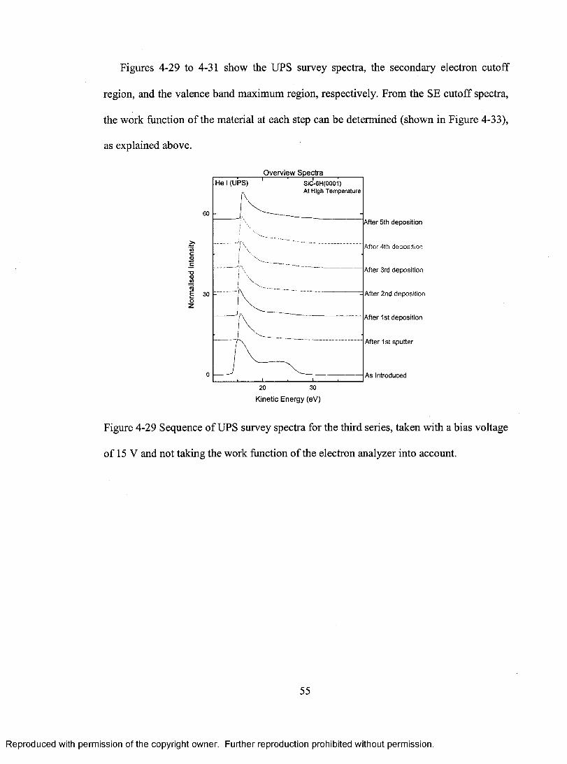
Figures 4-29 to 4-31 show the UPS survey spectra, the secondary electron cutoff
region, and the valence band maximum region, respectively. From the SE cutoff spectra,
the work function of the material at each step can be determined (shown in Figure 4-33),
as explained above.
II
Overview Spectra _____SIC-6H(0001)At High Temperature
He I (UPS)
60After 5th deposition
After 4th deposition
After 3rd deposition
After 2nd deposition30
After 1st deposition
After 1st sputter
0 As Introduced20 30
Kinetic Energy (eV)
Figure 4-29 Sequence of UPS survey spectra for the third series, taken with a bias voltage
of 15 V and not taking the work function of the electron analyzer into account.
55
Reproduced with permission of the copyright owner. Further reproduction prohibited without permission.

SEcutoff Spectra
- He I (UPS) SC-6H(0001)At High Tem perature After 5th deposition
After 4th deposition
40 After 3rd depositionIcAfter 2nd depostition
After 1st depositionoz
After sputtering
As Introduced
14 1513 16
Kinetic Energy (eV)
Figure 4-30 Secondary electron cut-off spectra of the third sample series.
U pper VB S p ec tra
He I (UPS) SiC-6H(0001) Pd-deposition @ 800°C
■D
5th deposition 4th deposition3rd deposition
2nd deposition 1st deposition
After sputter As Introduced
3 2 1 0
Binding E nergy (eV)
Figure 4-31 Upper valence band spectra of the third series.
56
Reproduced with permission of the copyright owner. Further reproduction prohibited without permission.

From the spectra of the upper valence band, the valence band maximum can be
determined as explained earlier. As the Pd deposition increases, the VBM shifts to lower
binding energies, indicating that the sample is increasingly acquiring a metallic character
at the surface.
F erm i E n e rg y o f Au0.0
?
(U1.0
m
6H-SIC(0001) Pd-deposition ' @ high temp.
2.05thdeposition
A s a f t e r 1 s t 2 n d . . . . . .In tro d u ced s p u t t e r d e p o s i t i o n d e p o s i t i o n deposition d ep o s itio n deposition
3rd 4 thdeposition
Figure 4-32 Position of the valence band maximum/Fermi edge for the third sample
series.
The work function of the sample was measured and plotted in Figure 4-33. It
increases gradually and hence indicating that the sample converts gradually to Pd metal.
57
Reproduced with permission of the copyright owner. Further reproduction prohibited without permission.

_6H-SiC(0001)_ Pd-deposition @ 800°C
4.6
4.4
4.2
.9 4.0oc3u_ 3.8
I 3.6
3.4
3.2
3.0
1s t 2 nd 3 rddeposition deposition depositlwi deposition deposition
4thAs 5thAfterintroduced sp u tte r
Figure 4-33 Work Function plot of the sample at each step.
4.4 Discussions
If a metal and semiconductor are brought into contact (as shown in Figure 4-34),
generally a Schottky barrier is formed. The electrons start to flow from the semiconductor
into the metal (if the work function of the metal is greater than that of semiconductor)
until the Fermi energies of both solids are equal (equilibrium condition). In the
semiconductor, a depletion region of width W is formed (uncompensated donors). In the
metal, the electron transfer forms a negative surface charge layer. An electric field is
created and hence an electric potential, which results in a band bending [38].
58
Reproduced with permission of the copyright owner. Further reproduction prohibited without permission.

Energy
Metal
‘Vacuum level
Semiconductor
Bulk region
Fermi Level i ' I
ZFigure 4-34 Formation of a Schottky barrier (for the case of metal with a larger work
function than the semiconductor, as in the present case).
Note that the work function (O), i.e., the minimal energy required to remove an
electron from the Fermi level to vacuum level, is a surface property and not defined for
the bulk of a material (since no vacuum level is defined for the bulk). Nevertheless, most
textbooks depict a vacuum level even within the bulk of the material, which is incorrect.
In the diagrams of this thesis we have therefore included a hypothetical “bulk vacuum
level”, depicted by a wide-dashed line. In contrast, the vacuum level at the surface,
shown by the dotted line, is a well defined quantity. Since the work function is comprised
of the chemical potential (p) at the surface and the surface dipole (formed by a varying
degree of the electron wave functions extending into the vacuum), it is strongly
dependent on surface orientation and preparation. Furthermore, measurement is very
59
Reproduced with permission of the copyright owner. Further reproduction prohibited without permission.

sensitive to sample misalignment and local fields in the vacuum chamber. In our case, we
believe that, for example, the first data point in Fig. 4-33 is obscured by a misalignment
problem. In all of our work function measurements, it is possible that the absolute values
are too low, possibly due to a calibration problem. Nevertheless, differences between two
measured work functions are reliable and accurate to within 0.2 eV or better.
In the experiments of series 2, the sample was first cleaned by sputtering cycles and
then Pd was deposited layer by layer for five successive times. Figure 4-34 above shows
the formation of metal/semiconductor junction with a bulk metal on the surface of a
semiconductor where the work function of the metal is greater than that of the
semiconductor. In the present case, the metal/semiconductor interface was gradually
formed by stepwise deposition of Pd. As discussed above, the thinnest films don’t even
have a metallic character yet. We therefore have to augment the picture shown in Fig. 4-
34 to a step-wise approach, as will be shown in the following.
4.4.1 Sample state after the sputtering cycles
As the SiC sample was cleaned by sputtering cycles and no Pd was yet deposited at
this stage, the band structure of the sample is assumed to look as shown in Figure 4-35.
Note that we are assuming flat-hand conditions, which might not be the case in reality.
For example, well-defined surface states or surface resonances can lead to significant
charge accumulation at the surface, which induces a band bending. However, with
surface sensitive techniques (as in our case), it is not possible to derive the band bending
picture at the clean surface. We are hence assuming flat-hand conditions, noting that the
following discussion of band bending should be understood as a relative change with
respect to the band positions on the sputter-cleaned surface.
60
Reproduced with permission of the copyright owner. Further reproduction prohibited without permission.

In Figure 4-35, the measuring region on the sample, the work function of SiC (Osic),
the regions measured by XPS and UPS, and the surface and bulk regions of the sample
are shown.
IMeasuring Region
Iurfa<
"Vacuum level"
Fermi level
iceSiCBulk region
CBM
VBM \
2p
XPS,UPS
Figure 4-35 Band scheme of the sample after sputter-cleaning.
4.4.2 After the Pd deposition steps
After the first step, a very thin layer of Pd is formed on the SiC. The band scheme of
the metal-semiconductor interface can be drawn as in Figure 4-36.
61
Reproduced with permission of the copyright owner. Further reproduction prohibited without permission.

InterfaceDipole
SiCBulk region
I‘VacuufTjJeyer
mnl
FermiLevel
VBM \
tXPS,^UPS
-* z
Figure 4-36 Band scheme of the Pd-SiC interface after the Pd deposition.
Two different characteristic length scales need to be considered: on the scale of
several atomic layers, the chemical bond is formed, presumably including some
intermixing. This leads to a local and atom-specific shift of all electronic levels, as was
discussed above. In the case of Pd/SiC, there is apparently a different chemical
interaction for the room-temperature and the 800°C series, leading to a different shift for
Si and C, respectively. This shift, induced by charge transfer on a short length scale,
gives first indications on the chemical influence of Pd on SiC as a function of deposition
temperature.
62
Reproduced with permission of the copyright owner. Further reproduction prohibited without permission.

On the length scale of several hundred nanometers, electronic level alignment needs
to be considered, as for any metal-semiconductor interface. Because the work function of
SiC (4.8 eV) is less than that of Pd (5.1 eV), electrons will flow from SiC to Pd until the
Fermi levels of both are aligned. Hence, a depletion region is formed at the surface of
SiC. The negative charge accumulated at the metal and the uncompensated donors left at
the surface of SiC build a potential at the interface, which leads to a band bending in SiC.
Because, at first, only a very thin Pd layer is deposited, also the levels of the Pd shift
when electrons flow from SiC to Pd in order to equalize the Fermi levels. Hence, the
potential developed will be low and thus leads to a reduced bending of SiC bands. The
work function (associated with the vacuum level), which, as mentioned above, is purely a
property of the sample surface, increases, starting at the SiC work function and
approaching the Pd work function with increasing coverage.
As the thickness of deposited Pd increases, the number of electrons that flow from
SiC to Pd in order to align the Fermi levels increases which leads to an increase in band
bending of the SiC bands, as shown in Figure 4-37. Once the Pd layer has reached a
critical thickness, it will be sufficiently developed to supply the necessary screening
charges for a fully-developed Schottky barrier. No further shifts of the bands are
expected, even though there will still be some changes in the photoemission spectra,
since the probing volume is increasingly moved into the Pd layer and away from the SiC
“bulk”. Thus, for the thickest Pd layer on SiC in our experimental series, the band scheme
of the sample will be similar to that of a bulk metal-semiconductor Schottky junction.
63
Reproduced with permission of the copyright owner. Further reproduction prohibited without permission.

>.Inierfaca
Dipole
/ SiCBulk region
SurfaceDipoleI
“Vacuumlevel"
mat
FermiLevel
VB
XPS,UPS
z
Figure 4-37 Band scheme of the Pd-SiC interface after further Pd deposition.
It is important to note that such band schemes are significantly complicated by the
presence of dipoles, both at the surface (as discussed above) and the interface. In the
latter case, short-range charge transfer can add to an overall electrostatic field at the
interface, which would introduce a step in the hypothetical vacuum levels at the interface.
Such interface dipoles can substantially influence the electronic behavior of junctions,
and are indicative of a short-range mutual interaction of the junction partners. Finally, it
is important to note that most (real-world) interfaces show some degree of intermixing,
which might add to the complication of taking an interface dipole into account by
“smearing out” this dipole across an extended range near the interface.
64
Reproduced with permission of the copyright owner. Further reproduction prohibited without permission.

CHAPTER 5
CONCLUSIONS AND FUTURE WORK
5.1 Conclusions
In order to investigate the surface and interface properties of Pd/SiC and their
chemical bonding behavior, which is the starting point to understand the diffusion and
corrosion behavior of metal fission products (Pd) in TRISO coating materials, three
experimental series were prepared. In the first series, a well ordered SiC(OOOl) surface
was prepared and a monolayer of Pd was deposited onto the SiC single erystal at room
temperature. The SiC substrate in series 2 was intentionally structurally disordered by
extensive Ar-ion sputtering cyeles with 2 keV ions to simulate the crystalline structure of
TRISO SiC layers, which are not single-crystalline. The metal/semiconductor interface
was formed at room temperature and the Pd layer thickness was successively increased.
In order to study the impact of elevated temperatures, the SiC substrate in series 3 was
not only structurally disordered (as in series 2), but the metal/semiconductor interface
was also formed at higher temperatures (approx. at 800°C).
In series 1, two distinct carbon species on the SiC surface and three carbon species for
the Pd/SiC interface were found. The two main species could be ascribed to a SiC bulk
species and an interface species. In parallel, the Si 2p core levels also show the existenee
of two different Si species, both before and after the interface formation. In both cases,
there is an upward shift of all electronic levels, which indicates a change in surface band
65
Reproduced with permission of the copyright owner. Further reproduction prohibited without permission.

bending o f the SiC substrate due to the formation of the metal/semiconductor interface.
In series 2, three chemical carbon species and two Si 2p species existed at the clean
and uncovered SiC(OOOl) surface, which again can be ascribed to a bulk and an
interface/surface species (a third species with low intensity was ascribed to adventitious
carbon). The strong increase in intensity of the interface species during Pd deposition
suggests an intermixing at the interface. There is a shift of all main peaks o f the SiC
substrate towards smaller binding energies, indicating a change in surface band bending
of the SiC substrate due to the formation of the metal/semiconductor interface.
Comparing the results of series 2 (room temperature) and 3 (800°C), we find significant
differences in the local chemical environment of Si atoms upon the first Pd deposition
step, indicating a different (temperature-dependent) reaction mechanism between Pd and
SiC. For further steps, the evolution of the Pd/SiC interface, in particular in view of an
upward band bending and the formation of a Schottky barrier, appears to be similar in
both cases.
Thus, in summary, all the three experimental series shows an upward shift o f all
electronic levels indicating that there is band bending induced in the SiC substrate when
Pd is deposited. Furthermore, there is significant charge transfer between Pd and SiC on
various length scales. The interface species of all the species in all the experimental series
is getting dominant as a function of Pd coverage, which is interpreted as a significant
intermixing at the interface. Hence one can conclude that Pd interacts with SiC in several
different ways, inducing local chemical bonding (corrosion), intermixing, and electronic
structure modification. This, in turn, will impact the degradation of the SiC layer by Pd,
potentially leading to coating failure in TRISO nuclear fuel.
66
Reproduced with permission of the copyright owner. Further reproduction prohibited without permission.

5.2 Future Work
For structural information, the samples described above are currently also being
investigated with Transmission Electron Microscopy (TEM) for cross-sectional studies.
Further analysis on Pd/SiC interface can be done by using X-ray Absorption
Spectroscopy (XAS) and X-ray Emission Spectroscopy (XES). The results obtained
should be tested by performing experiments on real TRISO SiC layers.
Based on the current experiments, it will be of large interest to conduct further
experimental series by forming the Pd/SiC interface at even higher temperatures and by
modifying the SiC surface prior to interface formation, e.g., by suitable plasma-etching
procedures.
67
Reproduced with permission of the copyright owner. Further reproduction prohibited without permission.
BIBLIOGRAPHY
[1] R.L. Murray, Nuclear Energy, Technology and Industrial Arts (2000).
[2] K.Minato, K.Fukuda, A.Ishikawa, N.Mita, Advanced coatings for HTGR fuel particles against corrosion of SiC layer, J. Nucl. Mat. 246 (1997) 215.
[3] B.F. Myers, E C. Montgomery, and K.E. Partain, Doc No. 909055, GA Technologies Inc., (1986).
[4] R.J. Lauf, T.B. Lindemer, and R.L. Pearson, Out-of-reactor Studies of Fission Product-Silicon Carbide Interactions in HTGR Particles, 172 (1990) 184.
[5] Ronald L. Hockey, Pacific Northwest National Laboratory, Innovative Low-Cost Approaches to Automating QA/QC of Fuel Particle Production Using On-line Nondestructive Methods for Higher Reliability, Proposal Number: 2002-103
[6] E. E. Morris and T. H. Bauer, Modeling of the Repository Behaviour of TRISO fuel, ANL-AFCI-160 (2005).
[7] K. Minato, T. Ogawa, K. Fukuda, K. Ikawa, and K. Iwamoto, Electron Probe Microanalysis of Irradiated Triso-Coated U02 Particles (II), Japan Atomic Energy Research Institute, Report JAERI-M 84-002 (1984).
[8] T.N. Tiegs, Fission-Product Pd-SiC interaction in Irradiated Coated-Particle Fuels, Nucl. Technol. 57 (1982) 389.
[9] F. Montgomery, Fission Product-SiC Reaction in HTGR Fuel, General Atomic Company, Report DOE/ET/35300-T3 (1981).
[10] K. Minato, T. Ogawa, K. Fukuda, S. Kashimura, M. Shimizu and Y. Tayama, Fission Product Palladium-Silicon Carbide Interaction in HTGR Fuel Particles, J. Nucl. Mat. 172 (1990) 184.
[11] C. Heske, Interaction between metal fission products and TRISO coating materials:A study of chemical bonding and interdiffusion. Proposal for Task 17, Transmutation Research Program, UNLV.
[12] L.I. Johansson, F. Owman, and P. Martensson, High-Resolution core-level study of 6H-SiC(0001), Physical Review B 53 (1996) 20.
68
Reproduced with permission of the copyright owner. Further reproduction prohibited without permission.

[13] L. Li and I.S.T. Tsong, Surf. Sci., 351 (1996) 141.
[14] F. Owman, and P. Martensson, Surf. Sci., 369 (1996) 126.
[15] Y. Hoshino, T. Nishimura, T. Yoneda, K. Ogawa, H. Namba and Y. Kido, Initial oxidation of 6H-SiC(0001)- V3xV3 surface studied by ion scattering combined with photoemission induced by synchrotron-radiation-light, Surface Science 505 (2002) 234.
[16] J. Bernhardt, M. Nerding, U. Starke and K. Heinz, Stable surface reconstructions on 6H-SiC(000 I ), Materials Science and Engineering B6I-62 (1999) 207.
[17] A. Seubert, J. Bernhardt, M. Nerding, U. Starke, and K. Heinz, In situ surface phases and silicon-adatom geometry of the (2x2)c structure on 6H-SiC(000 1 ), Surface Science 454-456 (2000) 45-48.
[18] B. F. Rider, Compilation of Fission Product Yields, General Electric Company, GE Report NEDO-I2154-3 (1981).
[19] T. Namba, K. Minato, M. Yamawaki, and F. Fukuda, A Study on the Reaction between SiC and Pd, Japan Atomic Energy Research Institute, Report JAERI-M, 87-218 (1988).
[20] H. Kleykamp, The Behavior of Fission Products in Highly Burnt HTR Fuels by Microprobe Analysis, Kemforschungszentrum Karlsruhe, Report KfK 2213 (1975).
[21] R. Benz, R. Forthmann, H. Grubmeier, and A. Naoumidis, in: Thermodynamics o f Nuclear Materials 1979, Vol. I (IAEA, Vienna, 1980) p. 565.
[22] K. Minato, T. Ogawa, K. Fukuda, K. Ikawa, and K. Iwamoto, Electron Probe Microanalysis of Irradiated Triso-Coated U02 Particles (I), Japan Atomic Energy Research Institute, Report JAERI-M 83-200 (1983).
[23] H. Kleykamp, J. Nucl. Mater. 131 (1985) 221.
[24] K. Naito, T. Tsuji, T. Matsui, and A. Date, J. Nucl. Mater. 154 (1988) 3.
[25] D. Petti, and J. Maki, The Challenges Assoicted with High Bumup and High Temperature for UO2 TRISO-Coated Particle Fuel, Idaho National Laboratory, MIT NGNP Symposium.
[26] C. L. Smith, SiC-Fission Product Reactions in Triso UC2 and WAR UCxOy Fissile Fuel, Part I: Kinetics of Reactions in a Thermal Gradient, GA-A14313, General Atomic Company (Sep. 1977); also J. Am. Ceram. Soc. 62, 600 (1979).
69
Reproduced with permission of the copyright owner. Further reproduction prohibited without permission.

[27] R. L. Pearson, and T. B. Lindemer, The Interaction of LaCz and NdC] with SiC in HTGR Particles, Proc. Topl. Mtg. Thermal Reactor Safety, CONF-770708, Vol. 3, p.357, U.S. Department of Energy (1977).
[28] Akio Kotani and Shik Shin, Resonant inelastic x-ray scattering spectra for electrons in solids. Rev. o f Modern Physics 73 (2001) 203.
[29] C.Heske, Spectroscopic investigation of buried interfaces and liquids with soft X- rays; Appl. Phys. A 78 (2004) 829-835.
[30] S. Hüfiier: Photoelectron Spectroscopy (Springer Ser. Solid-State Sci. 82) (Springer, Berlin, Heindelberg 1995).
[31] D.Briggs and M.P.Seah, Practical Surface Analysis, second edition, volume I, Chichester; New York: Wiley, 1983.
[32] http://www.uksaf.org/tech/xps.html
[33] R. L. Murray, Nuclear Energy: An Introduction to the Concepts, Systems, and Applications of Nuclear Process, Elsevier, fifth edition, 1920.
[34] http://www.mcallister.com/evappage.html
[35] A. Al-Hilfy, and R. Loudon, Effects of broadening mechanisms on atomic resonance fluorescence, J. Phys. B: At. Mol. Phys. 15 (1982) 2819.
[36] P.P. Me Cluskey, R. Grzybowski, and T. Podlesak, High Temperature Electronics, pIOI, 1996.
[37] Nieuwenhuys, Bouwman, and Sachtler, Thin Solid Films, 21,51,1974.
[38] A. Hiraki, Metal-Semiconductor Interfaces, first edition, Japan, 1995, lOS press.
[39] L. Lindell, P. de Jong, W. Ocikowicz, R. Lazzaroni, M. Berggren, W. R. Salaneck,X. Crispin, Characterization of the interface dipole at the paraphenylenediamine-nickel interface: A joint theoretical and experimental study, J. of Chem. Phys., 122, 084712 (2005).
70
Reproduced with permission of the copyright owner. Further reproduction prohibited without permission.

VITA
Graduate College University of Nevada, Las Vegas
Goverdhan Reddy Gajjala
Local Address:969 E Flamingo RdApartment #135Las Vegas, Nevada 89119
Permanent Address:Neelaiguda, Tripuraram mandai Nalgonda Dt., Andhra Pradesh India-508207.
Degree:
Conferences:
Thesis Title:
Bachelor of Science, Electrical Engineering, 2003 Osmania University College of Engineering, India
Arizona-Nevada Academy of Science (ANAS) at UNLV, Feb. 2005
American Nuclear Society (ANS) Conference at Ohio State University, Ohio, April 2005.
Interaction between Pd and SiC: a Study for TRISO Nuclear Fuel
Thesis Examination Committee:Chairperson, Dr. Rama Venkat, Ph. D.Committee Member, Dr. Biswajit Das, Ph. D.Committee Member, Dr. Sahjendra Singh, Ph. D.Graduate Faculty Representative, Dr. Clemens Heske, Ph. D.
71
Reproduced with permission of the copyright owner. Further reproduction prohibited without permission.