Embed Size (px)
Citation preview
1 C3M0025065D Rev 1, 12-2020
C3M0025065DSilicon Carbide Power MOSFET C3M
TM MOSFET Technology
N-Channel Enhancement Mode Features
• 3rd Generation SiC MOSFET technology• High blocking voltage with low on-resistance• High speed switching with low capacitances• Fast intrinsic diode with low reverse recovery (Qrr)• Halogen free, RoHS compliant
Benefits
• Higher system efficiency• Reduced cooling requirements• Increased power density• Increased system switching frequency• Easy to parallel and simple to drive • Enable new hard switching PFC topologies (Totem-Pole)
Applications
• EV chargers • UPS• Solar inverters• Industrial SMPS• DC/DC converters
Package
Part Number Package Marking
C3M0025065D TO-247-3 C3M0025065D
VDS 650 V
ID @ 25˚C 97 A
RDS(on) 25 mΩ
Maximum Ratings
Symbol Parameter Value Unit Note
VDSS Drain - Source Voltage, TC = 25 ˚C 650 V
VGS Gate - Source voltage (Under transient events < 100 ns) -8/+19 V Fig. 29
ID
Continuous Drain Current, VGS = 15 V, TC = 25˚C 97A Fig. 19
Continuous Drain Current, VGS = 15 V, TC = 100˚C 70
ID(pulse) Pulsed Drain Current, Pulse width tP limited by Tjmax 251 A
PD Power Dissipation, TC=25˚C, TJ = 175 ˚C 326 W Fig. 20
TJ , TstgOperating Junction and Storage Temperature -40 to
+175 ˚C
TLSolder Temperature, 1.6mm (0.063”) from case for 10s 260 ˚C
Md Mounting Torque, (M3 or 6-32 screw) 18.8
Nmlbf-in
2 C3M0025065D Rev 1, 12-2020
Electrical Characteristics (TC = 25˚C unless otherwise specified)
Symbol Parameter Min. Typ. Max. Unit Test Conditions Note
V(BR)DSS Drain-Source Breakdown Voltage 650 V VGS = 0 V, ID = 100 μA
VGSon Gate-Source Recommended Turn-On Voltage 15 VStatic Fig. 29
VGSoff Gate-Source Recommended Turn-Off Voltage -4 V
VGS(th) Gate Threshold Voltage1.8 2.3 3.6 V VDS = VGS, ID = 9.22 mA
Fig. 111.9 V VDS = VGS, ID = 9.22 mA, TJ = 175ºC
IDSS Zero Gate Voltage Drain Current 1 50 μA VDS = 650 V, VGS = 0 V
IGSS Gate-Source Leakage Current 10 250 nA VGS = 15 V, VDS = 0 V
RDS(on) Drain-Source On-State Resistance 25 34
mΩVGS = 15 V, ID = 33.5 A Fig. 4,
5,6 33 VGS = 15 V, ID = 33.5 A, TJ = 175ºC
gfs Transconductance25
SVDS= 20 V, IDS= 33.5 A
Fig. 724 VDS= 20 V, IDS= 33.5 A, TJ = 175ºC
Ciss Input Capacitance 2980
pF
VGS = 0 V, VDS = 0V to 600 V
F = 1 MhzVAC = 25 mV
Fig. 17, 18
Coss Output Capacitance 178
Crss Reverse Transfer Capacitance 12
Co(er) Effective Output Capacitance (Energy Related) 236VGS = 0 V, VDS = 0V to 400 V
Note: 1
Co(tr) Effective Output Capacitance (Time Related) 340 Note: 1
Eoss Coss Stored Energy 37 μJ VDS = 600 V, F = 1 Mhz Fig. 16
EON Turn-On Switching Energy (Body Diode) 578μJ
VDS = 400 V, VGS = -4 V/15 V, ID = 33.5 A, RG(ext) = 2.5 Ω, L= 59 μH, TJ = 175ºC
FWD = Internal Body Diode of MOSFET
Fig. 25EOFF Turn Off Switching Energy (Body Diode) 214
EON Turn-On Switching Energy (External Diode) 392μJ
VDS = 400 V, VGS = -4 V/15 V, ID = 33.5 A, RG(ext) = 2.5 Ω, L= 59 μH, TJ = 175ºC
FWD = External SiC DIODE
Fig. 25EOFF Turn Off Switching Energy (External Diode) 238
td(on) Turn-On Delay Time 14
ns
VDD = 400 V, VGS = -4 V/15 VID = 33.5 A, RG(ext) = 2.5 ΩTiming relative to VDS Inductive load
Fig. 26tr Rise Time 60
td(off) Turn-Off Delay Time 27
tf Fall Time 12
RG(int) Internal Gate Resistance 1.3 Ω f = 1 MHz, VAC = 25 mV
Qgs Gate to Source Charge 29
nCVDS = 400 V, VGS = -4 V/15 VID = 33.5 APer IEC60747-8-4 pg 21
Fig. 12Qgd Gate to Drain Charge 37
Qg Total Gate Charge 108
Note (1): Co(er), a lumped capacitance that gives same stored energy as Coss while Vds is rising from 0 to 400V Co(tr), a lumped capacitance that gives same charging time as Coss while Vds is rising from 0 to 400V
3 C3M0025065D Rev 1, 12-2020
Reverse Diode Characteristics (TC = 25˚C unless otherwise specified)
Symbol Parameter Typ. Max. Unit Test Conditions Note
VSD Diode Forward Voltage5.0 V VGS = -4 V, ISD = 16.8 A, TJ = 25 °C Fig. 8,
9, 104.5 V VGS = -4 V, ISD = 16.8 A, TJ = 175 °C
IS Continuous Diode Forward Current 52 A VGS = -4 V, TC = 25˚C
IS, pulse Diode pulse Current 251 A VGS = -4 V, pulse width tP limited by Tjmax
trr Reverse Recover time 33 nsVGS = -4 V, ISD = 33.5 A, VR = 400 Vdif/dt = 745 A/µs, TJ = 175 °CQrr Reverse Recovery Charge 309 nC
Irrm Peak Reverse Recovery Current 17 A
trr Reverse Recover time 51 nsVGS = -4 V, ISD = 33.5 A, VR = 400 Vdif/dt = 685 A/µs, TJ = 175 °C
Qrr Reverse Recovery Charge 261 nC
Irrm Peak Reverse Recovery Current 12 A
Thermal Characteristics
Symbol Parameter Typ. Unit Test Conditions Note
RθJC Thermal Resistance from Junction to Case 0.46°C/W Fig. 21
RθJA Thermal Resistance From Junction to Ambient 40
4 C3M0025065D Rev 1, 12-2020
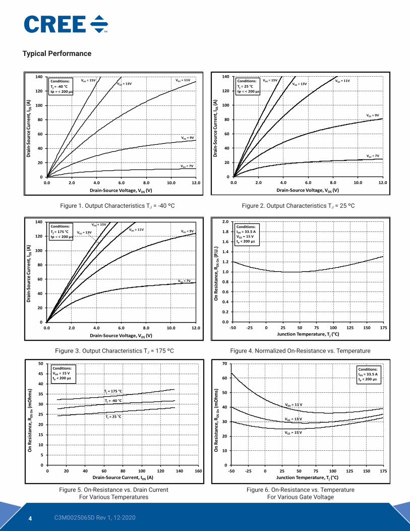
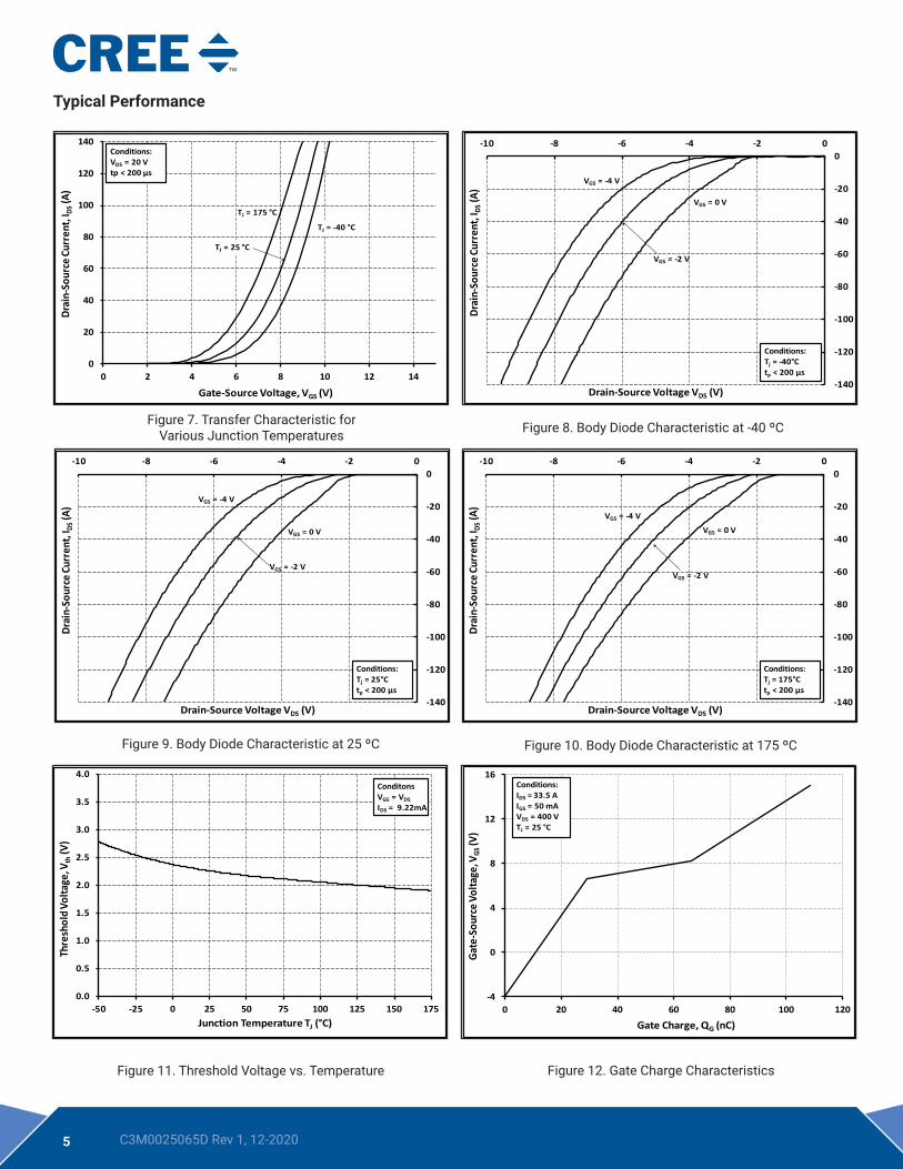
Figure 2. Output Characteristics TJ = 25 ºC
Typical Performance
Figure 5. On-Resistance vs. Drain CurrentFor Various Temperatures
Figure 1. Output Characteristics TJ = -40 ºC
Figure 3. Output Characteristics TJ = 175 ºC
0.0
0.2
0.4
0.6
0.8
1.0
1.2
1.4
1.6
1.8
2.0
-50 -25 0 25 50 75 100 125 150 175
On R
esist
ance
, RDS
On
(P.U
.)
Junction Temperature, Tj (°C)
Conditions:IDS = 33.5 AVGS = 15 Vtp < 200 µs
0
5
10
15
20
25
30
35
40
45
50
0 20 40 60 80 100 120 140 160
On
Resi
stan
ce, R
DS O
n(m
Ohm
s)
Drain-Source Current, IDS (A)
Conditions:VGS = 15 Vtp < 200 µs
Tj = 175 °C
Tj = -40 °C
Tj = 25 °C
Figure 4. Normalized On-Resistance vs. Temperature
0
10
20
30
40
50
60
70
-50 -25 0 25 50 75 100 125 150 175
On
Resi
stan
ce, R
DS O
n(m
Ohm
s)
Junction Temperature, Tj (°C)
Conditions:IDS = 33.5 Atp < 200 µs
VGS = 15 V
VGS = 13 V
VGS = 11 V
Figure 6. On-Resistance vs. TemperatureFor Various Gate Voltage
0
20
40
60
80
100
120
140
0.0 2.0 4.0 6.0 8.0 10.0 12.0
Drai
n-So
urce
Curr
ent,
I DS(A
)
Drain-Source Voltage, VDS (V)
Conditions:Tj = 175 °Ctp = < 200 µs
VGS = 7V
VGS = 13VVGS = 11V VGS = 9V
VGS = 15V
0
20
40
60
80
100
120
140
0.0 2.0 4.0 6.0 8.0 10.0 12.0
Drai
n-So
urce
Curr
ent,
I DS(A
)
Drain-Source Voltage, VDS (V)
Conditions:Tj = 25 °Ctp = < 200 µs
VGS = 7V
VGS = 13VVGS = 11V
VGS = 9V
VGS = 15V
0
20
40
60
80
100
120
140
0.0 2.0 4.0 6.0 8.0 10.0 12.0
Drai
n-So
urce
Curr
ent,
I DS(A
)
Drain-Source Voltage, VDS (V)
Conditions:Tj = -40 °Ctp = < 200 µs
VGS = 7V
VGS = 13VVGS = 11V
VGS = 9V
VGS = 15V
5 C3M0025065D Rev 1, 12-2020
Typical Performance
Figure 8. Body Diode Characteristic at -40 ºC
Figure 9. Body Diode Characteristic at 25 ºC
0
20
40
60
80
100
120
140
0 2 4 6 8 10 12 14
Drai
n-So
urce
Cur
rent
, IDS
(A)
Gate-Source Voltage, VGS (V)
Conditions:VDS = 20 Vtp < 200 µs
TJ = 25 °C
TJ = -40 °C
TJ = 175 °C
-140
-120
-100
-80
-60
-40
-20
0-10 -8 -6 -4 -2 0
Drai
n-So
urce
Cur
rent
, IDS
(A)
Drain-Source Voltage VDS (V)
Conditions:Tj = -40°Ctp < 200 µs
VGS = -2 V
VGS = -4 V
VGS = 0 V
-140
-120
-100
-80
-60
-40
-20
0-10 -8 -6 -4 -2 0
Drai
n-So
urce
Cur
rent
, IDS
(A)
Drain-Source Voltage VDS (V)
Conditions:Tj = 25°Ctp < 200 µs
VGS = -2 V
VGS = -4 V
VGS = 0 V
-140
-120
-100
-80
-60
-40
-20
0-10 -8 -6 -4 -2 0
Drai
n-So
urce
Cur
rent
, IDS
(A)
Drain-Source Voltage VDS (V)
Conditions:Tj = 175°Ctp < 200 µs
VGS = -2 V
VGS = -4 V
VGS = 0 V
0.0
0.5
1.0
1.5
2.0
2.5
3.0
3.5
4.0
-50 -25 0 25 50 75 100 125 150 175
Thre
shol
d Vo
ltage
, Vth
(V)
Junction Temperature TJ (°C)
ConditonsVGS = VDSIDS = 9.22mA
Figure 10. Body Diode Characteristic at 175 ºC
-4
0
4
8
12
16
0 20 40 60 80 100 120
Gate
-Sou
rce
Volta
ge, V
GS(V
)
Gate Charge, QG (nC)
Conditions:IDS = IGS = 50 mAVDS = TJ = 25 °C
33.5 A
400 V
Figure 7. Transfer Characteristic for Various Junction Temperatures
Figure 11. Threshold Voltage vs. Temperature Figure 12. Gate Charge Characteristics
6 C3M0025065D Rev 1, 12-2020
Typical Performance
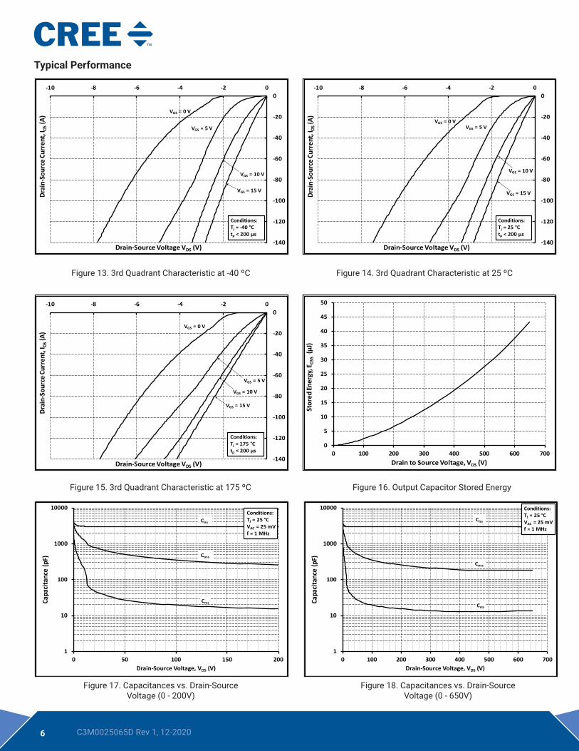
Figure 15. 3rd Quadrant Characteristic at 175 ºC
Figure 13. 3rd Quadrant Characteristic at -40 ºC
-140
-120
-100
-80
-60
-40
-20
0-10 -8 -6 -4 -2 0
Drai
n-So
urce
Cur
rent
, IDS
(A)
Drain-Source Voltage VDS (V)
Conditions:Tj = -40 °Ctp < 200 µs
VGS = 10 V
VGS = 5 V
VGS = 15 V
VGS = 0 V
-140
-120
-100
-80
-60
-40
-20
0-10 -8 -6 -4 -2 0
Drai
n-So
urce
Cur
rent
, IDS
(A)
Drain-Source Voltage VDS (V)
Conditions:Tj = 25 °Ctp < 200 µs
VGS = 10 V
VGS = 5 V
VGS = 15 V
VGS = 0 V
-140
-120
-100
-80
-60
-40
-20
0-10 -8 -6 -4 -2 0
Drai
n-So
urce
Cur
rent
, IDS
(A)
Drain-Source Voltage VDS (V)
Conditions:Tj = 175 °Ctp < 200 µs
VGS = 10 V
VGS = 5 V
VGS = 15 V
VGS = 0 V
Figure 14. 3rd Quadrant Characteristic at 25 ºC
0
5
10
15
20
25
30
35
40
45
50
0 100 200 300 400 500 600 700
Stor
ed En
ergy
, EO
SS(µ
J)
Drain to Source Voltage, VDS (V)
Figure 16. Output Capacitor Stored Energy
Figure 17. Capacitances vs. Drain-Source Voltage (0 - 200V)
1
10
100
1000
10000
0 50 100 150 200
Capa
cita
nce
(pF)
Drain-Source Voltage, VDS (V)
Ciss
Coss
Conditions:TJ = 25 °CVAC = 25 mVf = 1 MHz
Crss
1
10
100
1000
10000
0 100 200 300 400 500 600 700
Capa
cita
nce
(pF)
Drain-Source Voltage, VDS (V)
Ciss
Coss
Conditions:TJ = 25 °CVAC = 25 mVf = 1 MHz
Crss
Figure 18. Capacitances vs. Drain-Source Voltage (0 - 650V)
7 C3M0025065D Rev 1, 12-2020
1E-3
10E-3
100E-3
1
1E-6 10E-6 100E-6 1E-3 10E-3 100E-3 1
Junc
tion
To C
ase
Impe
danc
e, Z
thJC
(o C/W
)
Time, tp (s)
0.5
0.3
0.1
0.05
0.02
0.01
SinglePulse
Typical Performance
0
10
20
30
40
50
60
70
80
90
100
-50 -25 0 25 50 75 100 125 150 175
Drai
n-So
urce
Con
tinou
s Cur
rent
, IDS
(DC)
(A)
Case Temperature, TC (°C)
Conditions:TJ ≤ 175 °C
0
50
100
150
200
250
300
350
-50 -25 0 25 50 75 100 125 150 175
Max
imum
Dis
sipa
ted
Pow
er, P
tot(W
)
Case Temperature, TC (°C)
Conditions:TJ ≤ 175 °C
0.01
0.10
1.00
10.00
100.00
1000.00
0.1 1 10 100 1000
Drai
n-So
urce
Cur
rent
, IDS
(A)
Drain-Source Voltage, VDS (V)
100 µs
1 ms
10 µs
Conditions:TC = 25 °CD = 0, Parameter: tp
100 ms
Limited by RDS On1 µs
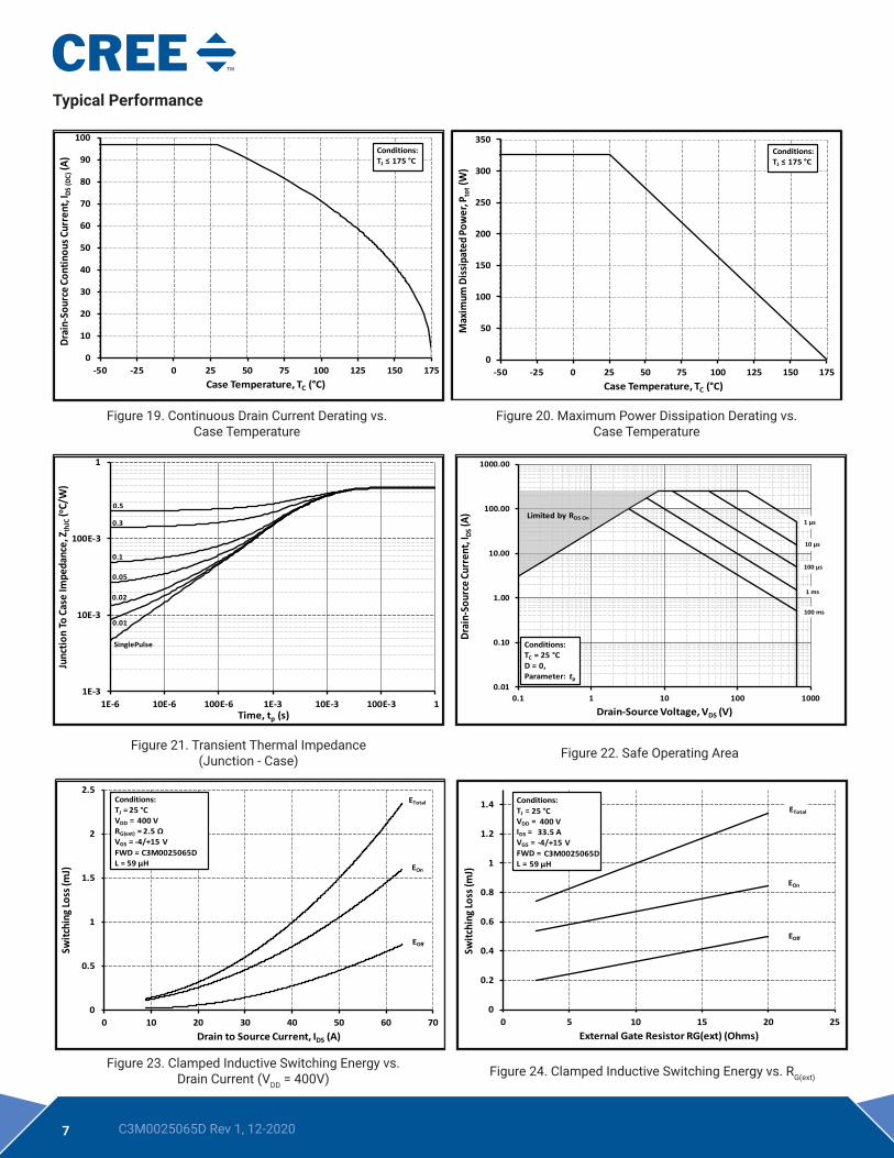
Figure 22. Safe Operating AreaFigure 21. Transient Thermal Impedance(Junction - Case)
0
0.5
1
1.5
2
2.5
0 10 20 30 40 50 60 70
Switc
hing
Loss
(mJ)
Drain to Source Current, IDS (A)
EOff
EOn
ETotalConditions:TJ = VDD = RG(ext) = VGS = FWD = L =
25 °C400 V
2.5 Ω-4/+15 V
C3M0025065D59 μH
Figure 23. Clamped Inductive Switching Energy vs. Drain Current (VDD = 400V)
Figure 19. Continuous Drain Current Derating vs. Case Temperature
Figure 20. Maximum Power Dissipation Derating vs. Case Temperature
0
0.2
0.4
0.6
0.8
1
1.2
1.4
0 5 10 15 20 25
Switc
hing
Loss
(mJ)
External Gate Resistor RG(ext) (Ohms)
EOff
EOn
ETotal
Conditions:TJ = VDD = IDS = VGS = FWD = L =
25 °C400 V
33.5 A-4/+15 V
C3M0025065D59 μH
Figure 24. Clamped Inductive Switching Energy vs. RG(ext)

8 C3M0025065D Rev 1, 12-2020
Typical Performance
0
0.2
0.4
0.6
0.8
1
1.2
0 25 50 75 100 125 150 175 200
Switc
hing
Loss
(mJ)
Junction Temperature, TJ (°C)
EOff
EOn
ETotal
Conditions:IDS = VDD = RG(ext) = VGS = L = FWD =FWD =
33.5 A 400 V
2.5 Ω-4/+15 V
59 μH C3M0025065D
ETotal with Schottky
EOn with Schottky
EOff with Schottky
C3D16065A
Figure 25. Clamped Inductive Switching Energy vs. Temperature
Figure 26. Switching Times vs. RG(ext)
0
20
40
60
80
100
120
0 5 10 15 20 25
Switc
hing
Tim
es (n
s)
External Gate Resistor RG(ext) (Ohms)
td(off)
Conditions:TJ = VDD = IDS = VGS = FWD =
tr
tf
td(on)
25 °C400 V
33.5 A-4/+15 V
C3M0025065D
9 C3M0025065D Rev 1, 12-2020
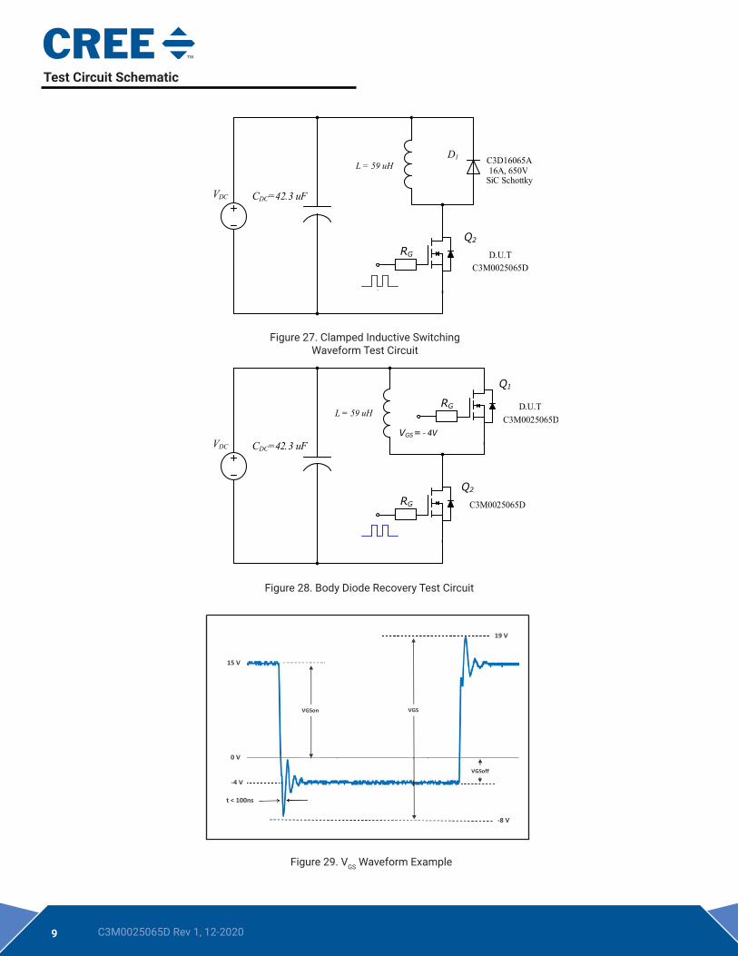
Test Circuit Schematic
Figure 28. Body Diode Recovery Test Circuit
Figure 27. Clamped Inductive Switching Waveform Test Circuit
D1 C4D10120A10A, 1200VSiC Schottky
D.U.TC2M0080120D
L=156 uH
Q2
VDC
D.U.TC2M0080120D
Q1
VGS= - 5V
C2M0080120D
RG
RG
CDC=42.3 uF
L=156 uH
Q2
VDC
RG
CDC=42.3 uF
C4D20120A20A, 1200VSiC Schottky
D.U.TC3M0060065K
D.U.TC3M0060065K
C3M0060065K
L= 135 µH
L= 135 µH
L = 57.6 µH
L = 57.6 µH
C3M0015065K
C3M0015065K
C3M0015065K
C3M0015065D
C3M0015065D
C3M0015065D
V
L = 59 uH
C3M0025065D
C3M0025065D
C3M0025065D
L = 59 uH
C3D16065A 16A, 650V
Figure 29. VGS Waveform ExampleCREE CONFIDENTIAL & PROPRIETARY © 2018 Cree, Inc. All rights reserved. Cree®, the Cree logo, Wolfspeed®, and the Wolfspeed logo are registered trademarks of Cree, Inc.3
VGSon VGS
15 V
19 V
0 V
t < 100ns
-4 V
VGSoff
-8 V
10 C3M0025065D Rev 1, 12-2020
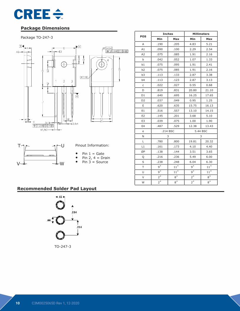
Package Dimensions
Package TO-247-3
Recommended Solder Pad Layout
TO-247-3
POSInches Millimeters
Min Max Min Max
A .190 .205 4.83 5.21
A1 .090 .100 2.29 2.54
A2 .075 .085 1.91 2.16
b .042 .052 1.07 1.33
b1 .075 .095 1.91 2.41
b2 .075 .085 1.91 2.16
b3 .113 .133 2.87 3.38
b4 .113 .123 2.87 3.13
c .022 .027 0.55 0.68
D .819 .831 20.80 21.10
D1 .640 .695 16.25 17.65
D2 .037 .049 0.95 1.25
E .620 .635 15.75 16.13
E1 .516 .557 13.10 14.15
E2 .145 .201 3.68 5.10
E3 .039 .075 1.00 1.90
E4 .487 .529 12.38 13.43
e .214 BSC 5.44 BSC
N 3 3
L .780 .800 19.81 20.32
L1 .161 .173 4.10 4.40
ØP .138 .144 3.51 3.65
Q .216 .236 5.49 6.00
S .238 .248 6.04 6.30
T 9˚ 11˚ 9˚ 11˚
U 9˚ 11˚ 9˚ 11˚
V 2˚ 8˚ 2˚ 8˚
W 2˚ 8˚ 2˚ 8˚
Pinout Information:
• Pin 1 = Gate• Pin 2, 4 = Drain • Pin 3 = Source
T U
WV
1111 C3M0025065D Rev 1, 12-2020
Copyright © 2020 Cree, Inc. All rights reserved. The information in this document is subject to change without notice. Cree, the Cree logo, and Zero Recovery are registered trademarks of Cree, Inc.
Cree, Inc.4600 Silicon Drive
Durham, NC 27703USA Tel: +1.919.313.5300
Fax: +1.919.313.5451www.wolfspeed.com/power
• RoHS Compliance The levels of RoHS restricted materials in this product are below the maximum concentration values (also referred to as the threshold limits) permitted for such substances, or are used in an exempted application, in accordance with EU Directive 2011/65/EC (RoHS2), as implemented January 2, 2013. RoHS Declarations for this product can be obtained from your Cree representative or from the Product Documentation sections of www.cree.com.
• REACh Compliance REACh substances of high concern (SVHCs) information is available for this product. Since the European Chemical Agency (ECHA) has published notice of their intent to frequently revise the SVHC listing for the foreseeable future,please contact a Cree represen-tative to insure you get the most up-to-date REACh SVHC Declaration. REACh banned substance information (REACh Article 67) is also available upon request.
• This product has not been designed or tested for use in, and is not intended for use in, applications implanted into the human body nor in applications in which failure of the product could lead to death, personal injury or property damage, including but not limited to equipment used in the operation of nuclear facilities, life-support machines, cardiac defibrillators or similar emergency medical equipment, aircraft navigation or communication or control systems, air traffic control systems.
Notes
Related Links
• SPICE Models: http://wolfspeed.com/power/tools-and-support
• SiC MOSFET Isolated Gate Driver reference design: http://wolfspeed.com/power/tools-and-support
• SiC MOSFET Evaluation Board: http://wolfspeed.com/power/tools-and-support