Embed Size (px)
Citation preview
INTERACTION EFFECT OF RCA DILUTION, TEMPERATURE AND MEGASONIC ON
PARTICLE REMOVAL EFFICIENCY, GATE OXIDE QUALITY, DEFECT DENSITY AND YIELD
Jane Chai Hai Sing
Master of Engineering 2009
P1l53t Khidmat Maklumat Akademik UNtVERSm MALAYSIA SARAWAJ(
P,KHIDMAT MAKLUMAT AKADEMIK
1llIllIlIlli'ITillllllllll 1000246131
INTERACTION EFFECT OF RCA DILUTION, TEMPERATURE AND MEGASONIC ON PARTICLE REMOVAL EFFICIENCY, GATE OXIDE
QUALITY, DEFECT DENSITY AND YIELD
JANE CHAI HAl SING
Thesis Submitted To Faculty of Engineering, Univerisiti Malaysia Sarawak
In Fulfillment of the Requirements for the Masters in Engineering (Electronics and Telecommunication 2009)
ACKNOWLEDGEMENTS
I would like to acknowledge the constructive contributions of Prof. Dr.
Khairuddin Abdul Hamid for his guidelines and information for the thesis. He
has spent his precious time in discussing the thesis, which could not have been
written without his help.
Very valuable assistance was also provided by Mdm. Siti Kudnie and Dr. Mohd
Saufee Muhammad who provided a great deal of suggestions in the preparation
of the thesis writing.
I would also like to express my appreciation to 18t Silicon Sdn. Bhd. (X-Fab
Foundry Sdn. Bhd.), which provided me the environment and information
necessary for the research.
Finally, I would like to say thank you to my husband, daughter and parents for
providing me with morale support and motivation.
ii
ABSTRAK
Proses pembersihan RCA (Radio Corporation of America) yang
diubahsuai menjadi pilihan kebanyakan pengeluar peranti untuk memenuhi
keperluan ketat ITRS (International Technology Roadmap for Semiconductor)
kerana kos penglibatan yang rendah dan masa kitaran yang pendek. Oleh itu,
pemahaman kesan saling tindak pembolehubah RCA dari segi kualiti
pembersihan partikel yang berlain_an saiz dan kualiti silikon dioksida adalah
penting. Seperkara lagi, proses pembersihan kini menghadapi masalah
kerosakan struktur bagi peranti bergeometri kecil. Dalam tesis ini,
kemungkinan penggunaan megasonik di QDR (Quick Dump Rinse) dikaji.
Objektif utama adalah untuk mewujudkan proses pembersihan optimum
dengan kos minimum. Proses pembersihan optimum ditentukan oleh kualiti
pembersihan partikel, silikon dioksida dan kecacatan ke atas wafer. Tiga
eksperimen ini dilaksanakan berdasarkan perbezaan suhu, masa pemprosesan,
kuasa megasonik dan pencairan RCA melalui penggunaan DOE (Design of
Experiment). Hasil keputusan ini disahkan dengan pemeriksaan ujian elektrik
dan die berguna. Pencairan 'RCA dengan masa pemprosesan yang lebih pendek
dan suhu yang lebih tinggi untuk hanya SCI (Standard Clean 1) menujukkan
kecekapan pembersihan yang lebih baik dan silikon dioksida yang berkualiti.
Berteraskan interaksi kajian, tambahan penggunaan megasonic di QDR
berupaya memantapkan kecekapan pembersihan tanpa struktur rosak. Proses
pembersihan RCA yang baru menunjukkan keputusan drive current dan die
berguna yang lebih baik.
ill

,.... I
ABSTRACT
Tweaking RCA (Radio Corporation of America) cleaning process has been
the choice of many manufacturers in order to meet the stringent requirement of
ITRS (International Technology Roadmap for Semiconductor) as the
involvement cost and cycle time is low. It is necessary to understand the
interaction effect of RCA variables in term of particle size and gate oxide
quality. In addition, the current cleaning process facing pattern damage issue
for smaller geometry integrated circuit. In this thesis, tre possibility of using
megasonic in QDR (Quick Dump Rinse) is studied. The main objective is to
establish optimize cleaning process which able to outperform the standard
cleaning with minimum cost. The optimized cleaning process is determined by
particle removal efficiency, gate oxide quality and defect density. The three
experiments are carried out based on different temperature, processing time,
megasonic power and dilution. The runs are computed using DOE (Design of
Experiment). The obtained result is further confIrmed by checking electrical test
and sort yield. Diluted RCA with shorter processing time and higher
temperature for SC-I (Standard Clean 1) only demonstrate better cleaning
efficiency and gate oxide quality. Based on this interaction study, additional
megasonic in QDR after SC-I is able to maintain the cleaning efficiency without
pattern damage. The optimized recipe outperforms in term of drive current and
sort yield.
iv
Pusat Khidmat MfakJumat Akademik UNlVERSm MALAYSIA SARAWAK
TABLE OF CONTENTS
Page
Acknowledgement 11
Abstrak ill
Abstract IV
List of Figures vm
List ofAbbreviations Xll
Table of Contents V
List of Tables x
Chapter 1 INTRODUCTION
1.1 Problem Definition 1
1.2 International Technology Roadmap fur 2 Semiconductor Requirement In Front-End Surface Preparation
1.3 Project Overview 4
1.4 Project Outline 6
1.5 Expected Contributions and Objectives 6
Chapter 2 LITERATURE REVIEW
2.1 Introduction to Semiconductor Technology 7
2.2 Introduction to Wafer Fabrication Process Step 8
2.3 Introduction to Wafer Fabrication Process 8 Module
v
2.4 Introduction to Wafer Surface Preparation
2.5 Contaminants
2.6 Existing Cleaning Processes for Semiconductors
2.7 Review of RCA Cleaning Process
2.8 Summary
Chapter 8 METHODOLOGY
3.1 Introduction
3.2 Design of Experiment
3.3 Evaluation Method
3.4 Particle Removal Efficiency Experiment
3.5 Quantox Analysis for RCA Variables in Pre-Gate Cleaning
3.6 Defect Data Collection on Short Loop Pattern Wafers
3.7 Final Experimenta1i with Pattern Wafers
3.8 Summary
Chapter 4 RESULTS, ANALYSIS, AND DISCUSSIONS
4.1 Introduction
4.2 Particle Removal Efficiency on Radio Corporation of America Cleaning Process and Megasonic Condition
4.2.1 Results and Discussions for Particle Removal Efficiency Percentage
4.2.2 Summary
11, 14
16
28
30
32
33
33
33
38
41
43
44
45
46
48
55
vi
4.3 Quantox Analysis for RCA Concentration, 55 Temperature and Processing Time
4.3.1 Results and Discussions for Quantox 56 Analysis
4.3.2 Summary 60
4.4 Defect Density Analysis for Different 61 Megasonic Power
4.4.1 Results and Discussions of Defect 63 Density for Different Megasonic Power
4.4.2 Summary 67
4.5 Split Run for Full Loop Pattern Wafer 67
4.5.1 Electrical Parameters Result 70 (Breakdown Voltage and Drive Current)
4.5.2 Yield Data Analysis 78
4.6 Summary 80
Chapter 5 CONCLUSIONS AND RECOMMENDATIONS
5.1 Introduction 81
5.2 Methodology Used 83
5.3 Problems Encountered 84
5.4 Limitations and Recommendations 85
5.5 Contributions of the study 86
REN RENCES 87
vii
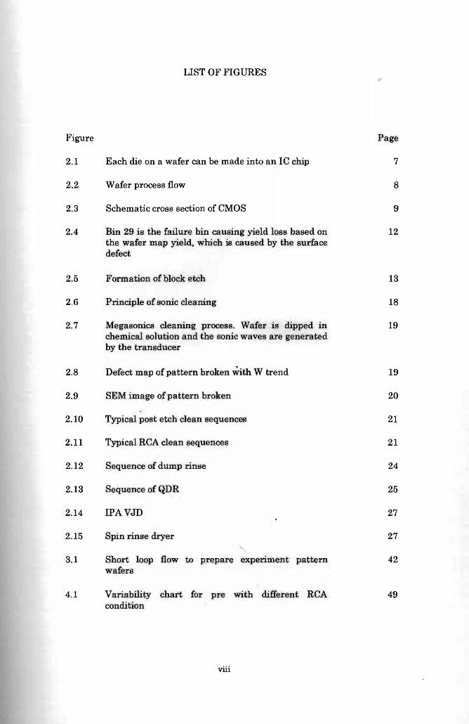
Figure
2.1
2.2
2.3
2.4
2.5
2.6
2.7
2.8
2.9
2.10
2.11
2.12
2.13
2.14
2.15
3.1
4.1
UST OF FIGURES
Page
Each die on a wafer can be made into an IC chip 7
Wafer process flow 8
Schematic cross section of CMOS 9
Bin 29 is the failure bin causing yield loss based on 12 the wafer map yield, which is caused by the surface defect
Formation of block etch 13
Principle of sonic cleaning 18
Megasonics cleaning process. Wafer is dipped in 19 chemical solution and the sonic waves are generated by the transducer
Defect map of pattern broken with W trend 19
SEM image of pattern broken 20
Typical post etch clean sequences 21
Typical RCA clean sequences 21
Sequence of dump rinse 24
Sequence of QDR 25
IPA VJD 27
Spin rinse dryer 27
Short loop flow to prepare experiment pattern 42 wafers
Variability chart for pre with different RCA 49 condition
viii

4.2
4.3
4.4
4.5
4.6
4.7
4.8
4.9
4.10
4.11
4.12
4.13
4.41
4.15
4.16
4.17
4.18
PRE% for different megasonic power in SC-1 and QDR bath (Based on SC-1 megasonic power group)
51
PRE% for different megasonic power in SC-1 and QDR bath (Based on QDR megasonic power group)
52
Variability chart result lifetime (microsecond)
for bulk. recombination 57
Variability chart for tunneling field (MV/Cm) 58
Variability chart for total charge X E10 (#/CmA2) 59
Variability chart for interface trap density X ElO [#/(Ev-Cm A 2)]
60
Variability graph for QDR megasonic power within SC-1 megasonic power
63
Variability graph of pattern broken percentage with different QDR and SC-1 megasonic power
65
Variability and t-test analysis of NMOS Breakdown voltage for high voltage
71
Variability and t-test analysis of PMOS breakdown voltage for high voltage
72
Variapility and t-test analysis of NMOS breakdown voltage for low voltage
73
Variability and t-test analysis of PMOS breakdown 74 voltage for low voltage
Variability and t-test current for high voltage
Varj.ability and t-test current for high voltage
Variability and t-test current for low voltage
Variability and t-test current for low voltage
analysis of NMOS drive 75
analysis of PMOS drive 76
analysis of NMOS drive 77
analysis of PMOS drive 78
Box plot comparison for yield 79
ix
IJST OF TABLES
Table Page
1.1 Surface preparation technology requirement - front 3 end process
2.1 Sources and related effects of various 15 contaminations
2.2 ITRS surface cleaning guides 16
2.3 Comparison of various wafer cleaning methods 17
3.1 Parameters detail for PRE experiment on RCA 34 condition
3.2 Setting for SC-1 and QDR megasonic power 34 evaluation
3.3 Recipe used for particle remova] efficiency 35 experiment
3.4 DOE table for RCA condition 36
3.5 DOE table for SC-1 and QDR megasonic power 37
3.6 Parameter setting for quantox analysis 39
3.7 DOE for quantox analysis experiment 40
3.8 Recipe used in quantox analysis 41
4.1 Proc.ess variable consideration 46
4.2 The DOE setting for SC-1 concentration and SC-2 47
4.3 DOE experiment runs 47
4.4 DOE table for SC-1 and QDR megasonic power 48
4.5 Summary results afDOE 50
4.6 Summary of quantox analysis result 61
x
4.7 Description of reClpe used for megasonic power 62 defect analysis
4.8 DOE table for different SC-1 and QDR megasonic 66 power with result
4.9 Evaluation recipe for engineering split 68
4.10 Baseline recipe for engineering split 68
4.11 Split table for engineering wafers 69
5.1 Mean and standard deviation table for yield 79
5.2 Comparison of current process and new process 82 developed
5.2 Advantages of the research 86
xi
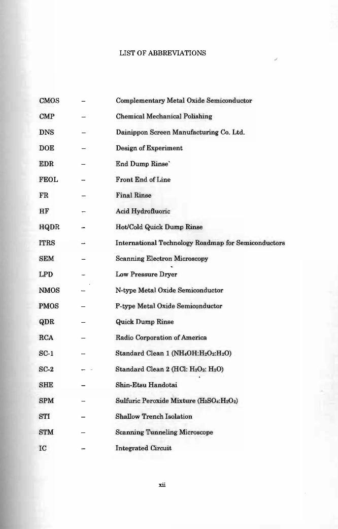
LIST OF ABBREVIATIONS
CMOS
CMP
DNS
DOE
EDR
FEOL
FR
HF
HQDR
ITRS
SEM
LPD
NMOS
PMOS
QDR
RCA
SC-l
SC-2
SHE
SPM
STI
STM
IC
Complementary Metal Oxide Semiconductor
Chemical Mechanical Polishing
Dainippon Screen Manufacturing Co. Ltd.
Design of Experiment
End Dump Rinse'
Front End of Line
Final Rinse
Acid Hydrofluoric
Hot/Cold Quick Dump Rinse
International Technology Roadmap for Semiconductors
Scanning Electron Microscopy
Low Pressure Dryer
N-type Metal Oxide Semiconductor
P-type Metal Oxide Semiconductor
Quick Dump Rinse
Radio Corporation of America
Standard Clean 1 (NH40H:H202:H20)
Standard Clean 2 (HCI: H202: H20)
Shin-Etsu Handotai
Sulfuric Peroxide Mixture (H2S04:H202)
Shallow Trench Isolation
Scanning Tunneling Microscope
Integrated Circuit
xii
GOI
IMEC
RIE
DIW
UV
IPA VJD
SRD
APM
PRE
Gate Oxide Integrity
Interuniversity Microelectronics Centre
Reactive Ion Etching
Deionised Water
illtraviolet
Isopropyl Alcohol Vapor Jet Dryer
Spin Rinse Dryer
Ammonium Peroxide Mixture(NH40H:H202:H20)
Particle Removal Efficiency
xiii

Chapter 1
INTRODUCTION
1.1 Problem Definition
Microprocessors, memories and logic devices require silicon-based CMOS
(Complementary Metal Oxide Semiconductor) technologies. Continuous
advances are being pursued in semiconductor industries in order to improve
device performance in ICs (Integrated Circuits). The removal of particles, on the
order of a micrometer and less in size, adhered to surfaces poses a challenge to
IC fabrication. As feature size decreases, smaller particles can mask a larger
portion of a pattern element. This will mean that part of the chip will not be
produced to specification and will lead to the rejection of the whole chip. Since
Moore's law [1] states that the number of transistors on an IC chips will be
double every two years, the problem will only get larger [1,2]. The stringent
surface contamination requirements outlined in the ITRS (International
Technology Roadmap for Semiconductors) pose new chaUenges for the surface
preparation technology.
Wet cleaning is the most frequeptly repeated step and vital in IC
production in order to prepare a smooth, particles and contamination free silicon
wafer surface. The RCA (Radio Corporation of America) clean which consists of
SC-l (Standard Clean 1) and SC-2 (Standard Clean 2) chemical developed in
1965 is the basis for most front-end wet cleaning process [3]. Megasonic is
1
introduced to assist the SC-1 solution in enhancing the particle removal
efficiency [4]. The conventional RCA cleaning and megasonic with concentrated
mixing ratio of chemical has increased the cost of production per wafer and also
directed to environment concerns. Besides this, conventional RCA cleaning with
megasonic cannot meet the ITRS requirement for nano-scale particles to be
removed from wafers surfaces without substrate damage or alteration [5]. This
study reflects the current issue facing for shrunken device manufacturer in
Malaysia. Through the comprehensive study of the effect of process variables in
wafer surface preparation, the problem can be narrowed down and helps to
develop a better process to overcome the issue. Simultaneously, a detail
understanding of wet cleaning process and the importance of the process to
wafer fabrication can be extended through the study.
1.2 International Technology Roadmap for Semiconductor
Requirement in Front-End Surface Preparation
ITRS identifies the technology requirement for wafer surface preparation
as shown in Table 1.1.
According to ITRS, it is clear that the density and size of killer defects
and particulate contamination will continue to be a concern at increasingly
demanding levels. AB feature sizes shrink, defects caused by particles during
silicon wafer production will have also effects on device yield as refer to Table
1.1 [6]. The critical particle diameter requirement continues to reduce from 50 to
32.5 nm [6], which imply that the particle removal efficiency for cleaning steps
have to be improved in order to cope the requisite. Studies have shown that
organic contamination at the interfaces of oxide-polysilicon gate stacks can
2
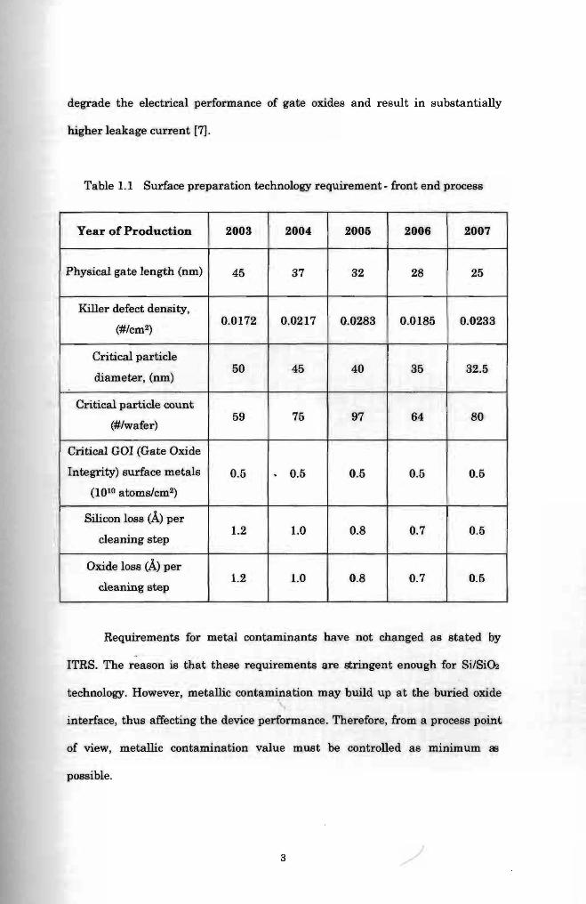
Year of Production I
2003 2004 2005 2006 2007
Physical gate length (nm) I
45 37 32 28 25
Killer defect density,
(#/cm2) I 0.0172 0.0217 0.0283 0.0185 0.0233
Critical particle
diameter, (nm) 50 45 40 35 32.5
I
I
I Critical particle count
(#/wafer) 59 I 75 97 64 80
Critical GO! (Gate Oxide
Integrity) surface metals
(1010 atomslcm2)
0.5 . 0.5
I
0.5 0.5 0.5
Silicon loss (1) per
cleaning step I
1.2 1.0 0.8 0.7 0.5
I
Oxide loss (1) per
cleaning step 1.2 1.0
I
0.8 0.7 0.5
degrade the electrical performance of gate oxides and result in substantially
higher leakage current [7] .
Table 1.1 Surface preparation technology requirement- front end process
I
I
j Requirements for metal contaminants have not changed as stated by
ITRS. The reason is that these requirements are stringent enough for SilSiDl
technology. However, metallic contamination may build up at the buried oxide
interface, thus affecting the device performance. Therefore, from a process point
of view, metallic contamination value must be controlled as minimum as
possible.
3
Next generation device characteristics will also require full control on the
silicon and oxide etched thickness during each process step. Final silicon vertical
dimension for source/drain junction depth in advanced CMOS technology are
around 200 A 16]. If the silicon under the source/drain extensions is recessed,
this changes the junction profile increasing the source/drain extension
resistance and decreasing drive currents. A critical layer in wafer fabrication
such as dual gate structure where oxide layer is used is critically responsive to
the final oxide thickness and direct impact the device voltage requirement. For
this reason, the silicon consumption of cleaning steps needs to be minimized and
perfectly controlled. With the current conventional RCA condition, it is
unworkable as the oxide and silicon loss is high, primarily due to ammonium
hydroxide mechanism [3].
1.3 Project Overview
As discussed earlier, with the decrease in the feature size of ICs,
particulate contamination poses a major challenge. A new method is needed
which should provide sufficient driving force for particle removal and should not
damage the wafer. The process should also achieve a minimum level of
cleanliness in a dependable manner with the least silicon and oxide loss as per
ITRS requirement. In order to meet these criteria, several new processes have
been introduced such as laser cleaning, IMEC (Interuniversity Microelectronics
Centre) cleaning, new chemistry introduction such as diluted hydrofluoric acid,
ultra pure water rinsing and dry cleaning [5]. Although many researchers have
proven the new methods, it is impossible for a matured foundry to totally change
the process due to cost effectiveness issue with new tool purchasing and
4
t Khidmat Maklumat AkademlkPusa ..... 1 .a.~SIA SARAWAKUNlVERSm I·~
resources involved, cycle time contribution in transferring the process and most
of the time, customers are reluctant to change due to reliability issues. Thus, an
evaluation on the current cleaning method which is RCA clean is required to
meet the challenges mentioned as the cost involvement will be cut down with no
new tool purchasing required. In addition, transferring time will be reduced
sufficiently as it is not an entire process change and customers will be more
susceptible to accept these minimum changes.
Besides the above reasons, as of today, cost reduction and environment
awareness are the core missions of semiconductor industry. For simple circuits,
the cost per component is nearly inversely proportional to the number of
components, the result of the equivalent piece of semiconductor in the
equivalent package containing more components and gone through the same
process steps. The increase of chemical wastage from the industry has awakened
the environment concerns.
The primary focus of the research will be in comprehending the current
(traditional) RCA cleaning method and revising the studies done previously on
RCA process. Based on the understanding of the RCA process, a comprehensive
study on the process variables (concentration, temperature and processing time)
in term of particle removal efficiency and gate oxide strength will be made. In
addition, the effect of SC-2 and megasonic impact will be evaluated. In short, the
RCA process will be appraised in term of particle removal efficiency, quantox
measurement for gate oxide integrity check, defect density, electrical and yield.
Robustness of the newly developed recipes is clearly established and
demonstrate that the new recipe perform at least as well as the standard RCA.
5
1.4 Project Outline
Chapter 1 provides introduction to problem definition, ITRS requirement,
project overview, expected contributions and objective of the thesis. The next
chapter, Chapter 2, is the literature review of basic transistor formatio!,\
existing cleaning key features and understanding of previous work on RCA
process. Methodologies used and evaluation components are presented in
Chapter 3. Chapter 4 discusses the results of the evaluation. Results will be
illustrated with graphs. The last chapter, Chapter 5 will summarize the o\erall
conclusions of the project and discuss on limitations and recommendations.
1.5 Expected Contributions and Objectives
The objective of this thesis is to study the effect of process variables in
wafer surface preparation technique, RCA cleaning. Through this study, an
optimized cleaning process which able to outperform the standard cleaning and
can be accepted effortlessly by matured foundry is established.
6
Chapter 2
LITERATURE REVIEW
2.1 Introduction to Semiconductor Technology
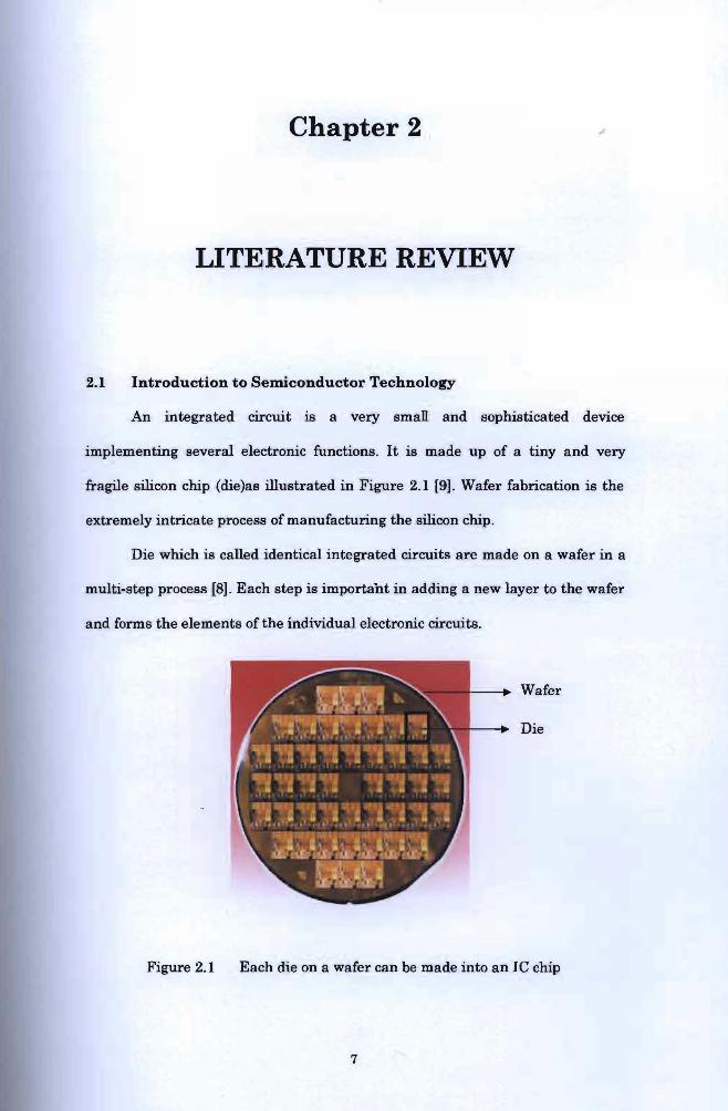
An integrated circuit is a very sman and sophisticated device
implementing several electronic functions. It is made up of a tiny and very
fragile silicon chip (die)as illustrated in Figure 2.1 [9]. Wafer fabrication is the
extremely intricate process of manufacturing the silicon chip.
Die which is called identical integrated circuits are made on a wafer in a
multi-step process [8]. Each step is importaht in adding a new layer to the wafer
and forms the elements of the individual electronic circuits.
Wafer
Die
Figure 2.1 Each die on a wafer can be made into an Ie chip
7
2.2 Introduction to Wafer Fabrication Process Step
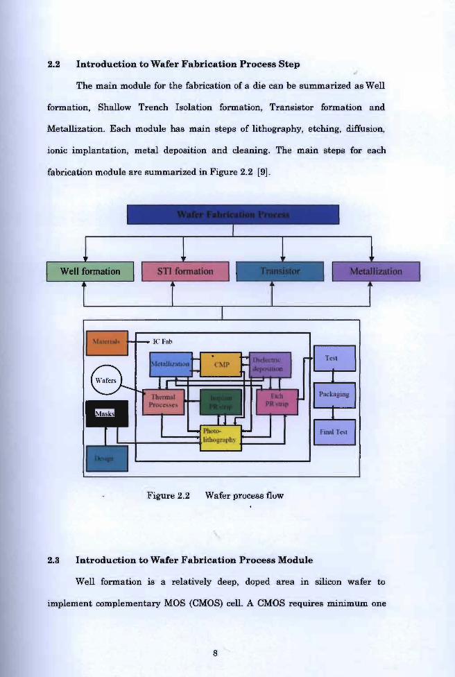
The main module for the fabrication of a die can be summarized as Well
formation, Shallow Trench Isolation formation, Transistor formation and
Metallization. Each module has main steps of lithography, etching, diffusion,
ionic implantation, metal deposition and cleaning. The main steps for each
fabrication module are summarized in Figure 2.2 [9].
Figure 2.2 Wafer process flow
2.3 Introduction to Wafer Fabrication Process Module
Well formation is a relatively deep, doped area in silicon wafer to
implement complementary MOS (CMOS) cell. A CMOS requires minimum one
8
well because NMOS requires a P background doping and PMOS requires an N
background doping. Well formation is important for a semiconductor device
having a high breakdown voltage and a low breakdown voltage transistor with
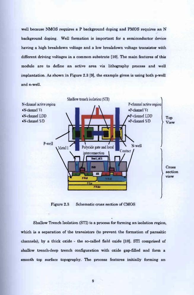
different driving voltages in a common substrate [10] . The main features of this
module are to define an active area via lith~aphy process and well
implantation. As shown in Figure 2.3 [9], the example given is using both powell
and newell.
Figure 2.3 Schematic cross section of CMOS
Shallow Trench Isolation (STI) is a process for forming an isolation region,
which is a separation of the transistors (to prevent the formation of parasitic
channels), by a thick oxide - the so-called field oxide [10] . STI comprised of
shallow trench-deep trench configuration with oxide gap-filled and form a
smooth top surface topography. The process features initially forming an
N-channel active region eN-ch..1lwel Vt eN-chaunel LDD eN-chaunel SiD
P-well
Shallow trench isolatioll (STI) P-channel active region eP-chawlel Vt P-chawlel LDD Top
View
Cross section view
9
insulator (oxide) trench shape, planarized through chemical mechanical
polishing (CMP).
Transistor formation is an extensive processes which consist of gate oxide
and poly-silicon formation, repeating photolithography and implantation
processes. The gate oxide formation is the most crucial step in CMOS technology.
The actual gate oxide is only a few nanometers thick and needs a dry oxidation
step which produces the best oxide quality [11]. Immediately after the gate
oxidation polysilicon is deposited, form the gate electrode. To achieve sufficient
conductivity, polysilicon has to be doped. Poly silicon doping can be done by
implantation or by diffusion from the gas phase the transistor gates which
define the channels of the MOS transistors are structured by the third
lithographic step followed by plasma etching [12]. For the definition of source
and drain areas of the n-channel transistor the p-channel transistors have to be
covered by a photoresist layer. Similar to the preceding source and drain
definition of the n-channel transistor, the p-channel source and drain regions
are formed.
Metallization is the formation of metal contacts and interconnects in the
manufacturing of semiconductor devices metal lines canprising of two or more
different metals deposited on top of each other and each serving different
purpose to obtain an integrated circuit; for instance, layer of aluminum will
assure low resistivity of metal contact while underlying titanium nitride willact
as a barrier preventing aluminum spiking [13]. Aluminum spiking normally
occurs at shallow p-n junctions formed on (1-0-0) oriented silicon substrates
during the high temperature metal alloy and will cause short circuit.
Interconnect scheme in integrated circuits implemented in several levels; metal
lines are stacked into several levels (as many as ten and more), are electrically
10