Embed Size (px)
Citation preview

Interface characterization of atomic layer deposited high-k on non-polar GaNYe Jia, Ke Zeng, and Uttam Singisetti
Citation: Journal of Applied Physics 122, 154104 (2017); doi: 10.1063/1.4986215View online: http://dx.doi.org/10.1063/1.4986215View Table of Contents: http://aip.scitation.org/toc/jap/122/15Published by the American Institute of Physics
Articles you may be interested in Initial leakage current paths in the vertical-type GaN-on-GaN Schottky barrier diodesApplied Physics Letters 111, 122102 (2017); 10.1063/1.4994627
Molecular beam epitaxial growth and characterization of AlN nanowall deep UV light emitting diodesApplied Physics Letters 111, 101103 (2017); 10.1063/1.4989551
Evolution and prevention of meltback etching: Case study of semipolar GaN growth on patterned siliconsubstratesJournal of Applied Physics 122, 105108 (2017); 10.1063/1.5001914
Defect quasi Fermi level control-based CN reduction in GaN: Evidence for the role of minority carriersApplied Physics Letters 111, 152101 (2017); 10.1063/1.5000720
Valence and conduction band offsets of β-Ga2O3/AlN heterojunctionApplied Physics Letters 111, 162105 (2017); 10.1063/1.5003930
Optical and structural study of deformation states in the GaN/AlN superlatticesJournal of Applied Physics 122, 155302 (2017); 10.1063/1.4999175

Interface characterization of atomic layer deposited high-k on non-polar GaN
Ye Jia, Ke Zeng, and Uttam Singisettia)
Department of Electrical Engineering, University at Buffalo, The State University of New York, Buffalo,New York 14260, USA
(Received 2 June 2017; accepted 30 September 2017; published online 18 October 2017)
The interface properties between dielectrics and semiconductors are crucial for electronic devices.
In this work, we report the electrical characterization of the interface properties between atomic
layer deposited Al2O3 and HfO2 on non-polar a-plane ð11�20Þ and m-plane ð1�100Þ GaN grown by
hybrid vapor phase epitaxy. A metal oxide semiconductor capacitor (MOSCAP) structure was used
to evaluate the interface properties. The impact of annealing on the interface properties was also
investigated. The border trap in the oxide, characterized by the capacitance-voltage (C-V) hysteresis
loop, was low. The interface state density (Dit), extracted using the ac conductance method, is in the
range of 0.5� 1012/cm2 eV to 7.5� 1011/cm2 eV within an energy range from 0.2 eV to 0.5 eV
below the conduction band minimum. The m-plane GaN MOSCAPs exhibited better interface prop-
erties than the a-plane GaN MOSCAPs after annealing. Without annealing, Al2O3 dielectrics had
higher border trap density and interface state density compared to HfO2 dielectrics. However, the
annealing had different impacts on Al2O3 dielectrics as compared to HfO2. Our results showed that
the annealing degraded the quality of the interface in HfO2, but it improved the quality of the inter-
face in Al2O3 devices. The annealing also reduced the positive trapped oxide charge, resulting in a
shift of C-V curves towards the positive bias region. Published by AIP Publishing.https://doi.org/10.1063/1.4986215
I. INTRODUCTION
GaN, a wide bandgap semiconductor, has been exten-
sively studied for a variety of applications such as power
amplifiers, power conversion devices, and light-emitting
diodes (LEDs) because of its large bandgap, high electron
mobility, high electron velocity, high breakdown voltage, and
the capability of forming various alloys.1–5 GaN is a polar
material with a wurtzite crystal structure, which results in a
large polarization field along the c-axis of the crystal6,7 which
is the traditional direction of the GaN crystal growth. The
polarization field has been used for polarization doping of het-
erostructures that show high electron mobilities.8,9 The polari-
zation field has been exploited to increase the hole density in
the p-type AlGaN/GaN heterojunction.10 However, for opto-
electronic devices, the separation of electron and hole wave-
functions due to the polarization field leads to a reduction of
the radiative emission rate.4,7,11 Moreover, the p-type doping
flexibility is reduced in polar GaN because of the polarity
inversion caused by the high Mg flux for achieving a high Mg
concentration.12–14 In recent years, novel non-polar GaN has
drawn a lot of attention for optoelectronic and electronic devi-
ces.15–18 Unlike the conventional polar GaN, the polarization
field is absent in the non-polar GaN crystal along the non-
polar direction.7,19 The absence of the polarization field in
non-polar GaN benefits both optoelectronic and electronic
devices.20,21 Non-polar optoelectronic device performance has
been greatly improved as compared to that of polar optoelec-
tronics devices, with reduction of the efficiency droop.11,22,23
The density function theory (DFT) predicts that the Fermi
level in p-type non-polar GaN is unpinned,24 which could
reduce the contact resistance to p-type GaN.14 We have
previously reported that the Fermi level in n-type non-polar
m-plane GaN was pinned close to mid-gap (�2.4 eV above
the valence band maximum).25 The low contact resistance to
p-type GaN is beneficial to heterostructure bipolar transistors
(HBTs) and p-channel devices.26,27 A normally off p-type
semi-polar GaN power device with high breakdown voltage
was demonstrated,28 which can also benefit from the low con-
tact resistance to p-type GaN.
Dielectrics are used as the gate barrier and passivation
layer in electronic devices. It is important to quantitatively
understand the interface electrical properties between the
dielectric layer and non-polar GaN for electronic applications.
Atomic layer deposition (ALD) has been widely used for
depositing a low interface state density high-k gate dielectric
layer on silicon, III-V materials, and emerging 2D materi-
als.10,29–33 The interface properties of ALD-dielectric/polar
GaN in terms of interface state density (Dit) have been studied
by the photo-assisted capacitance-voltage (CV) technique,34
the conductance method,34,35 and deep-level transient spec-
troscopy.36 The impact of thermal annealing on the interface
properties has also been investigated.34 However, there is
no report on the interface properties between dielectrics and
non-polar GaN. The band offsets between ALD-Al2O3 and
m-plane GaN characterized by x-ray photoelectron spectros-
copy have been reported,25 including the structural characteri-
zation. In this work, we evaluated the interface state density
and border trap density in ALD deposited high-k dielectrics
on a-plane and m-plane non-polar GaN.
II. EXPERIMENT DETAILS
The non-polar a-plane and m-plane bulk GaN wafers
were prepared at Kyma technologies Inc. The non-polar
GaN substrates were sliced from polar c-plane GaN whicha)[email protected]
0021-8979/2017/122(15)/154104/8/$30.00 Published by AIP Publishing.122, 154104-1
JOURNAL OF APPLIED PHYSICS 122, 154104 (2017)
was grown by hybrid vapor phase epitaxy (HVPE). The root
mean square (rms) roughness of the a-plane and m-plane
GaN substrates was 0.3 nm and 0.5 nm, respectively. The
van der Pauw Hall measurement gave an n-type conductivity
with a doping density of �1� 1016/cm3 for both samples.
The metal-oxide-semiconductor (MOSCAP) structures were
fabricated to study the interface properties. It is necessary to
form ohmic contacts to GaN in order to study the frequency
dependent capacitance-voltage profiles. It has been reported
that the contact resistance to GaN can be reduced by reactive
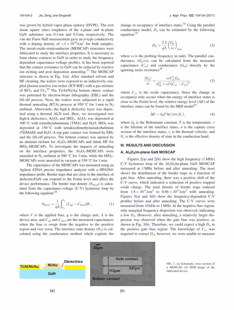
ion etching and post deposition annealing.37 The MOSCAP
structure is shown in Fig. 1(a). After standard solvent and
HF cleaning, the wafers were exposed to an inductively cou-
pled plasma reactive ion etcher (ICP-RIE) with a gas mixture
of BCl3 and Cl2.25 The Ti/Al/Ni/Au bottom ohmic contact
was patterned by electron-beam lithography (EBL) and the
lift-off process. Next, the wafers were subjected to a rapid
thermal annealing (RTA) process at 950 �C for 1 min in N2
ambient. Afterwards, the high-k dielectric layer was depos-
ited using a thermal ALD tool. Here, we investigated two
high-k dielectrics, Al2O3 and HfO2. Al2O3 was deposited at
300 �C with trimethylaluminum (TMA) and H2O. HfO2 was
deposited at 150 �C with tetrakis(dimethylamido)hafnium
(TDMAH) and H2O. A top gate contact was formed by EBL
and the lift-off process. The bottom contact was opened by
an alumina etchant for Al2O3-MOSCAPs and dilute HF for
HfO2-MOSCAPs. To investigate the impacts of annealing
on the interface properties, the Al2O3-MOSCAPs were
annealed in N2 ambient at 500 �C for 1 min, while the HfO2-
MOSCAPs were annealed in vacuum at 350 �C for 1 min.
The capacitance of the MOSCAPs was measured using an
Agilent 4294A precise impedance analyzer with a HP42941
impedance probe. Border traps that are close to the interface of
dielectric/GaN can respond to the Fermi level and affect the
device performance. The border trap density (Nbt,tot) is calcu-
lated from the capacitance-voltage (C-V) hysteresis loop by
the following equation:34
Nbt;tot ¼1
qA
ðV2
V1
jCup � CdwnjdV; (1)
where V is the applied bias, q is the charge unit, A is the
device area, and Cup and Cdwn are the measured capacitances
when the bias is swept from the negative to the positive
region and vice versa. The interface state density (Dit) is cal-
culated using the conductance method which exploits the
change in occupancy of interface states.35 Using the parallel
conductance model, Dit can be estimated by the following
equation:35
Dit ¼2:5
qA
Gp
x
� �max
; (2)
where x is the probing frequency in rad/s. The parallel con-
ductance, (Gp/x), can be calculated from the measured
capacitance (Cm) and conductance (Gm) directly by the
ignoring series resistance38
hGpix¼ x C2
oxGm
G2m þ x2 Cox � Cmð Þ2
; (3)
where Cox is the oxide capacitance. Since the change in
occupancy only occurs when the energy of interface states is
close to the Fermi level, the relative energy level (DE) of the
interface states can be found by the SRH model35
DE ¼ kBT ln srvtNcð Þ; (4)
where kB is the Boltzmann constant, T is the temperature, sis the lifetime of the interface states, r is the capture cross
section of the interface states, vt is the thermal velocity, and
Nc is the effective density of state in the conduction band.
III. RESULTS AND DISCUSSION
A. Al2O3/m-plane GaN MOSCAP
Figures 2(a) and 2(b) show the high frequency (1 MHz)
C-V hysteresis loop of the Al2O3/m-plane GaN MOSCAP
measured at 1 MHz before and after annealing. The inset
shows the distribution of the border traps as a function of
gate bias. After annealing, there was a positive shift of the
C-V curve, which indicated a reduction of positive trapped
oxide charge. The total density of border traps reduced
from 1.8� 1011/cm2 to 0.86� 1011/cm2 with annealing.
Figures 3(a) and 3(b) show the frequency-dependent C-V
profiles before and after annealing. The C-V curves were
measured from 10 kHz to 1 MHz. In the negative bias region,
only marginal frequency dispersion was observed, indicating
a low Dit. However, after annealing, a relatively larger dis-
persion was observed when the gate bias was positive, as
shown in Fig. 3(b). Therefore, we could expect a high Dit in
the positive gate bias region. The knowledge of Cox was
required to extract Dit; however, we were unable to measure
FIG. 1. (a) Schematic cross section of
a MOSCAP. (b) SEM image of the
fabricated device.
154104-2 Jia, Zeng, and Singisetti J. Appl. Phys. 122, 154104 (2017)

it directly from the GaN MOSCAPs due to the high leakage
current in the accumulation region, so we assumed that the
Cox of GaN devices would be the same as that of Si devices
that were fabricated simultaneously. Figure 4(a) shows the
calculated conductance peaks (Gp/x) as a function of fre-
quency using Eq. (3). The Gp/x peaks were measured from
�2 V to �10 V. It can be seen that when the bias was small
(�2 V to �5 V), the peak was modulated by the gate bias.
The peak shifted to lower frequency with the increasing gate
bias. When the gate bias was sufficiently large, the peak was
pinned at �200 Hz. The pinning of the Gp/x peaks can be
attributed to the bulk traps. Figure 4(b) shows the calculated
conductance peak as a function of frequency after annealing.
As indicated in Fig. 3, because the C-V curves shifted to the
positive bias region after annealing, the Gp/x peaks after
annealing were measured from þ2 V to �2 V. Similar to the
Gp/x peak before annealing, the conductance peak was modu-
lated by bias. The peak shifted from 6 MHz to 400 Hz when
the bias changed from 2 V to 0 V. When the bias moved to the
negative region, the peak shifted to a very low frequency which
was outside of the measurable range of the instrument at room
temperature. Figure 5 shows the calculated Dit as a function of
its energy level using Eq. (4) before and after annealing.
Before annealing, Dit ranged from �2.5� 1012 cm�2V�1 to
�5.0� 1012 cm�2V�1 and its energy ranged from 0.51 eV to
0.46 eV. Our reported Dit values were slightly higher than the
Dit of Al2O3/c-plane GaN reported by Winzer et al.34 in the
comparable energy range. After annealing, Dit was in the range
of 2.0� 1012 cm�2V�1 to 2.5� 1012 cm�2V�1 and Eit was
closer to conduction band minimum (CBM) compared to
before annealing. At an Eit of greater than 0.45 eV, Dit
decreased from 5� 1012 cm�2V�1 after annealing.
FIG. 2. C-V hysteresis loop of the
Al2O3/m-plane GaN device (a) before
annealing and (b) after annealing. The
insets show the distribution of the bor-
der traps as a function of gate bias.
After annealing, the C-V curves shifted
towards the positive bias region.
Reprinted with permission from Y. Jia
et al., Phys. Status Solidi B 254,
1600681 (2017). Copyright 2017 John
Wiley and Sons.
FIG. 3. Frequency-dependent C-V
curves of the Al2O3/m-plane GaN
device (a) before annealing and (b)
after annealing. A small frequency dis-
persion was observed at negative bias.
Reprinted with permission from Y. Jia
et al., Phys. Status Solidi B 254,
1600681 (2017). Copyright 2017 John
Wiley and Sons.
FIG. 4. Gp/x peak of the Al2O3/m-
plane GaN device (a) before annealing
and (b) after annealing. The peak was
modulated by bias. The peaks were
pinned at �200 Hz when the bias was
greater than �5 V.
154104-3 Jia, Zeng, and Singisetti J. Appl. Phys. 122, 154104 (2017)

B. HfO2/m-plane GaN MOSCAP
Figures 6(a) and 6(b) show the C-V hysteresis loop of
the HfO2/m-plane GaN MOSCAP measured at 1 MHz before
and after annealing. Similar to the Al2O3/m-plane GaN
MOSCAPs, there was a positive shift in the C-V curve after
annealing. The inset shows the calculated distribution of bor-
der traps as a function of gate bias. The border trap density
was calculated to be 1.0� 1011/cm2 before annealing and
1.9� 1011/cm2 after annealing. The annealing process
slightly increased the density of border traps. Figures 7(a)
and 7(b) show the frequency-dependent C-V profiles
measured from 1 kHz to 1 MHz pre- and post-annealing.
Similar to Al2O3/m-plane GaN MOSCAPs, a small fre-
quency dispersion in C-V curves was observed before
annealing. After annealing, C-V curves showed a large dis-
persion in the positive gate bias region, indicating a high Dit.
Figures 8(a) and 8(b) show the Gp/x peaks as a function of
frequency before and after annealing. In Fig. 8(a), it can be
seen that the position of the Gp/x peak at a gate bias of 1 V
was higher than 10 MHz which exceeded the measurement
capability and a partial peak was observed. While the posi-
tion of the Gp/x peak at a gate voltage of �1 V was lower
than the lower limit of the measurement frequency (100 Hz
not shown). Only one clear Gp/x peak was observed at a bias
of 0 V, which suggested that the interface states were close
to CBM and mid-gap. Similarly, in Fig. 8(b), after annealing,
there was no clear or complete Gp/x peak when the bias
became negative. Figure 9 shows the calculated Dit before
and after annealing within the measurable range. Before
annealing, Dit was about 2.5� 1012/cm2 eV�1 to 0.7� 1012/
cm2 eV�1 at an Eit in the range of 0.23–0.25 eV. As we men-
tioned above, the interface states were close to CBM. After
annealing, Dit increased to �7.5� 1012/cm2 eV at an Eit of
0.28 eV and �6.5� 1012/cm2 eV at an Eit of 0.35 eV. The
annealing process increased Dit. The effect of annealing on
HfO2-MOSCAPs was opposite to that of on Al2O3-
MOSCAPs. It should be noted that a temperature dependent
conductance measurement is necessary to probe more of the
interface states because at room temperature the measurable
range of Eit is limited.
FIG. 5. The calculated Dit of Al2O3/m-plane GaN devices before and after
annealing. Dit was found to be in the range of 2.5� 1012/cm2 eV to
5.0� 1012/cm2 eV without annealing. The annealing process reduced Dit.
FIG. 6. C-V hysteresis loop of the
HfO2/m-plane GaN device (a) before
annealing and (b) after annealing. The
insets show the distribution of the bor-
der traps as a function of gate bias.
After annealing, the C-V curves shifted
towards the positive bias region.
FIG. 7. Frequency-dependent C-V
curves of the HfO2/m-plane GaN
device (a) before annealing and (b)
after annealing. A small frequency dis-
persion was observed at negative bias.
154104-4 Jia, Zeng, and Singisetti J. Appl. Phys. 122, 154104 (2017)

C. Al2O3/a-plane GaN MOSCAP and HfO2/a-planeGaN MOSCAP
Unlike the m-plane GaN MOSCAPs, the a-plane GaN
MOSCAPs were characterized after the annealing process
because the MOSCAPs showed a high gate leakage current
before annealing. The devices were subjected to the same
annealing condition as m-plane GaN MOSCAPs. Figures 10(a)
and 10(b) show the C-V hysteresis loop of the Al2O3/a-plane
GaN MOSCAP and HfO2/a-plane GaN MOSCAP, respec-
tively. The insets show the corresponding border trap
distribution as a function of gate bias. In Fig. 10(a), it can be
seen that a slightly large dispersion was observed, indicating a
high Nbt inside the oxide. The C-V curves in the large negative
bias region did not show a depletion behavior, which could be
attributed to the high density of interface states and/or oxide
traps. In contrast, in Fig. 10(b), the HfO2/a-plane GaN
MOSCAP showed a flat C-V curve in the large negative bias
region. However, its C-V hysteresis loop exhibited a large dis-
persion between gate biases of 1 V and �3 V, indicating a high
Nbt. The inset of Fig. 10(a) showed a very broad distribution of
Nbt, giving an Nbt, tot of 2.7� 1011/cm2, whereas the inset of
Fig. 10(b) showed a narrow distribution of Nbt. However, the
peak reached a high value of 2.5� 1011/cm2, resulting in a
total Nbt, tot of 4.3� 1011/cm2. Figures 11(a) and 11(b) show
the frequency-dependent C-V curves of Al2O3/a-plane GaN
and HfO2/a-plane GaN MOSCAPs after annealing. The
measured frequencies for the Al2O3/a-plane GaN MOSCAP
were from 50 kHz to 1 MHz and for the HfO2/a-plane GaN
MOSCAP were from 1 kHz to 1 MHz. The bias of the Al2O3/
a-plane GaN MOSCAP was swept from 1 V to �5 V due to
high leakage current at low frequency. In Fig. 11(a), we can
see that there was a large frequency dispersion in the negative
bias region, suggesting a high Dit. However, the HfO2/a-plane
GaN MOSCAP revealed large dispersion in the positive bias
region. Figures 12(a) and 12(b) show the Gp/x peaks of
Al2O3/a-plane GaN and HfO2/a-plane GaN MOSCAPs. In Fig.
12(a), when the bias was greater than 1 V, the peak located at a
frequency of >10 MHz. With decreasing bias to the negative
region, the peak shifted to lower frequency and it was pinned
at �300 Hz when the bias was greater than �2 V. Figure 12(b)
FIG. 8. Gp/x peak of the HfO2/m-
plane GaN device (a) before annealing
and (b) after annealing. The peak was
modulated by bias. Only two peaks
were observed before and after
annealing.
FIG. 9. The calculated Dit of HfO2/m-plane GaN devices before and after
annealing. Dit was found to be in the range of 6� 1011/cm2 eV to 2.5� 1012/
cm2 eV without annealing. The annealing process increased Dit.
FIG. 10. C-V hysteresis loop of (a) the
Al2O3/a-plane GaN device and (b)
HfO2/a-plane GaN device after anneal-
ing. The insets show the distribution
of border traps as a function of bias.
Nbt, tot was higher than that of the m-
plane GaN device.
154104-5 Jia, Zeng, and Singisetti J. Appl. Phys. 122, 154104 (2017)

clearly shows voltage modulated Gp/x peaks from 2 V to 0 V.
However, when the bias was in the negative region, the Gp/xpeak was out of the measurable range. Figure 13 shows the cal-
culated Dit of the MOSCAPs. The Dit of the Al2O3/GaN device
was >8.5� 1012/cm2 eV at an Eit of 0.23 eV and �1.2� 1012/
cm2 eV at an Eit of 0.48 eV. When the gate bias changed from
�2 V to �4 V, Dit increased from �1.2� 1012/cm2 eV to
�4� 1012/cm2 eV. The Dit of the HfO2/GaN device changed
from 7.6� 1012/cm2 to 6.2� 1012/cm2 eV within the energy
range from 0.25 eV to 0.51 eV. Both Al2O3/a-plane GaN and
HfO2/a-plane GaN devices exhibited comparable interface
characteristics.
A summary of the characterization results is given in
Table I. For the device with Al2O3 as a dielectric layer, the
annealing process was beneficial to the reduction of Nbt, tot
inside the oxide and Dit at the interface. In contrast, the
annealing process, however, degenerated the interface of
HfO2/GaN devices by increasing Nbt, tot and Dit. However,
we need to note that the inadequate annealing process
might also contribute to this degeneration. In addition, the
annealing process removed the positive oxide charge,
leading to a shift of the C-V curve towards the positive
bias region. By comparing the polarity of GaN substrates,
the a-plane GaN MOSCAPs always exhibited higher Nbt,
tot and Dit than m-plane GaN MOSCAPs. Before anneal-
ing, HfO2 grown on GaN had the lowest Dit. If the device
was subjected to annealing, Al2O3 grown on GaN could
offer better quality of the interface. From these four devi-
ces, we can see that at room temperature, the lowest Eit
was close to �0.5 eV below the CBM. This value was
comparable to the DFT model, which is �0.7 eV below
CBM for m-plane GaN and �0.5 eV for a-plane GaN.24
Compared with the Nbt, tot of Al2O3/c-plane GaN reported
by Winzer et al.,34 our Al2O3/m-plane GaN MOSCAPs
showed low Nbt, tot, but it could be partially attributed to
the voltage sweeping range because of the incapability of
obtaining C-V curves at large positive bias due to the high
leakage current.
FIG. 11. Frequency-dependent C-V
curves of (a) the Al2O3/a-plane GaN
device and (b) HfO2/a-plane GaN
device after annealing. The Al2O3/a-
plane GaN device showed relatively
large frequency dispersion compared
to the HfO2/a-plane GaN device in the
negative bias region.
FIG. 12. Gp/x peak of (a) the Al2O3/a-
plane GaN device and (b) HfO2/m-
plane GaN device after annealing. The
peak was modulated by bias. The Gp/xpeak was pinned at �200 Hz probably
caused by bulk trap loss when bias was
greater than �1 V.
FIG. 13. The calculated Dit of the Al2O3/m-plane GaN device and (b) HfO2/
m-plane GaN device after annealing. In terms of Dit, both devices had com-
parable performance.
154104-6 Jia, Zeng, and Singisetti J. Appl. Phys. 122, 154104 (2017)

Without annealing, the Dit of the Al2O3 MOSCAP in
this work was higher than the Dit of the c-plane GaN device
reported in literatures for Ec–Eit> 0.4 eV characterized by
the conductance method (�4� 1011/cm2 eV–�6� 1011/cm2
eV),34 photo-assisted C-V method (�1.5� 1011/cm2 eV),39
and static C-V method (�2� 1011/cm2 eV).40 However, our
Dit was comparable to the Dit of the c-plane GaN device
reported in literatures for Ec–Eit> 0.4 eV characterized by
deep level transient spectroscopy (�3� 1011/cm2 eV–�8
� 1011/cm2 eV).41 With annealing at 500 �C in N2 ambient,
even though our devices showed a slight reduction of Dit
within an Eit in the range of 0.2 eV–0.4 eV as observed in the
literature,34 our Al2O3 MOSCAPs still revealed a high Dit
compared to that of the Al2O3/c-plane GaN devices with
annealing in N2 ambient for an Eit in the range of
0.2 eV–0.5 eV below the CBM characterized by the conduc-
tance method.34 However, our Al2O3 MOSCAPs showed a
much lower Dit than Al2O3/c-plane GaN devices with N2
annealing for an Eit in the range of 0.2 eV–0.5 eV below the
CBM (>3� 1011/cm2 eV) characterized by constant capaci-
tance deep level transient and optical spectroscopy reported
by Long et al.41 Compared to reported Dit at the Al2O3/m-
plane GaN interface (�1.5� 1012/cm2 eV for 0.2 eV–0.5 eV
below the CBM18,42), our post-annealed device showed a
similar Dit. The effect of annealing on Al2O3/non-polar GaN
is similar to its effect on the Al2O3/Si device.43 In our experi-
ment, the m-plane GaN devices exhibited similar interface
properties compared to c-plane GaN devices.
For the HfO2 MOSCAP, our results were slightly better
than the reported HfO2/c-plane GaN device44,45 even with
the annealing process. After annealing, at positive bias, the
leakage current and conductance increased significantly. The
degraded insulting properties of oxide can be partially
caused by the oxygen vacancies in the oxide.34 Additionally,
we cannot rule out the impacts of Ga native oxide regrowth
at the interface and the metal dangling bonds close to the
conduction band on the increase in interface states. Contrary
to our observation, a reduction of Dit was observed at the
sputtered HfO2/c-plane GaN interface46 and HfO2/Si with
the interfacial layer47 after N2 annealing. The degree of
reduction depends on the annealing atmosphere and tempera-
ture. Although the vacuum annealing improved the dielectric
constant (�25), it appeared that the annealing process also
introduced interface traps. On a-plane GaN, in terms of Dit,the HfO2 device had a slightly lower value than Al2O3, but
the difference was insignificant. However, this difference
was prone to be opposite on m-plane GaN. In fact, due to the
ignored resistance during the calculation of the conductance
peak (Gp/x), the resultant Dit could be overestimated or
underestimated. It also has been demonstrated that the
annealing condition has significant influence on the interface
properties in terms of Dit. In order to optimize the interface,
an appropriate condition should be used.
IV. SUMMARY
In summary, we characterized the interface properties of
ALD-dielectrics/non-polar GaN. The MOSCAPs that were
fabricated on a-plane and m-plane GaN substrates with
Al2O3 or HfO2 as a dielectric layer were used for the electri-
cal characterization. The impact of annealing on the density
of border traps and the density of interface traps was investi-
gated. The density of interface traps was extracted by the ac
conductance method. Prior to annealing, the density of inter-
face traps was in the magnitude of 1012, and it was one order
higher than the lowest reported Dit. Although the annealing
process brought down the Dit of Al2O3 devices as expected
in literatures, Dit was still higher than the best value. Further
optimization on the process, including but not limited to the
optimization of annealing conditions and the reduction of the
series resistance, may be required to reduce Dit. By reducing
leakage current, an accurate Cox can be obtained and the
interface traps close to the conduction band can be accessed.
Temperature dependent measurements can be conducted in
order to extract Dit located close to mid-gap.
ACKNOWLEDGMENTS
This work was supported by the ONR grant (No.
N000141310214) monitored by Dr. Paul A. Maki and by the
Innovative Micro-Programs Accelerating Collaboration in
Themes (IMPACT) program funded by the Office of Vice
President of Research and Economic Development at the
University at Buffalo. A portion of this work was performed
in the UB shared instrumentation facility.
1J. F. Muth, J. H. Lee, I. K. Shmagin, R. M. Kolbas, H. C. Casey, B. P.
Keller, U. K. Mishra, and S. P. DenBaars, Appl. Phys. Lett. 71, 2572
(1997).2D. C. Look, D. C. Reynolds, J. W. Hemsky, J. R. Sizelove, R. L. Jones,
and R. J. Molnar, Phys. Rev. Lett. 79, 2273 (1997).3Y. F. Wu, B. P. Keller, S. Keller, D. Kapolnek, P. Kozodoy, S. P.
Denbaars, and U. K. Mishra, Appl. Phys. Lett. 69, 1438 (1996).4S. Pimputkar, J. S. Specl, S. P. DenBaars, and S. Nakamura, Nat.
Photonics 3, 180 (2009).5J. Chen, S. Loeb, and J.-H. Kim, Environ. Sci.: Water Res. Technol. 3, 188
(2017).6E. T. Yu, X. Z. Dang, P. M. Asbeck, S. S. Lau, and G. J. Sullivan, J. Vac.
Sci. Technol. B 17, 1742 (1999).7C. Wetzel, M. Zhu, J. Senawiratne, T. Detchprohm, P. D. Persans, L. Liu,
E. A. Preble, and D. Hanser, J. Cryst. Growth 310, 3987 (2008).8Y. Fang, Z. Feng, J. Yin, X. Zhou, Y. Wang, G. Gu, X. Song, Y. Lv, C. Li,
and S. Cai, IEEE Trans. Electron Devices 61, 4084 (2014).9B. Reuters, A. Wille, N. Ketteniss, H. Hahn, B. Holl€ander, M. Heuken, H.
Kalisch, and A. Vescan, J. Electron. Mater. 42, 826 (2013).
TABLE I. Summary of the electrical characterization.
Device Al2O3/m-plane GaN HfO2/m-plane GaN Al2O3/a-plane GaN HfO2/a-plane GaN
Annealing Pre- Post- Pre- Post- Post- Post-
Nbt, tot (�1011/cm2) 1.8 0.86 1.0 1.9 2.7 4.3
Dit (�1012/cm2 eV) 5.0–2.5 2.5–1.9 2.0–0.7 7.5–6.5 8.5–1.2 7.7–6.2
Eit (eV) 0.46–0.51 0.23–0.5 0.23–0.25 0.27–0.35 0.23–0.48 0.25–0.52
154104-7 Jia, Zeng, and Singisetti J. Appl. Phys. 122, 154104 (2017)

10S. Kim, J. Nah, I. Jo, D. Shahrjerdi, L. Colombo, Z. Yao, E. Tutuc, and S.
K. Banerjee, Appl. Phys. Lett. 94, 062107 (2009).11G. Li, W. Wang, W. Yang, Y. Lin, H. Wang, Z. Lin, and S. Zhou, Rep.
Prog. Phys. 79, 056501 (2016).12V. Ramachandran, R. M. Feenstra, W. L. Sarney, L. Salamanca-Riba, J. E.
Northrup, L. T. Romano, and D. W. Greve, Appl. Phys. Lett. 75, 808 (1999).13S. Pezzagna, P. Venn�egues, N. Grandjean, and J. Massies, J. Cryst.
Growth 269, 249 (2004).14M. McLaurin, T. E. Mates, F. Wu, and J. S. Speck, J. Appl. Phys. 100,
063707 (2006).15M. C. Schmidt, K.-C. Kim, R. M. Farrell, D. F. Feezell, D. A. Cohen, M.
Saito, K. Fujito, J. S. Speck, S. P. DenBaars, and S. Nakamura, Jpn. J.
Appl. Phys., Part 2 46, L190 (2007).16A. Chakraborty, B. A. Haskell, S. Keller, J. S. Speck, S. P. Denbaars, S.
Nakamura, and U. K. Mishra, Jpn. J. Appl. Phys., Part 2 44, L173 (2005).17M. Ishida, M. Kuroda, T. Ueda, and T. Tanaka, Semicond. Sci. Technol.
27, 024019 (2012).18T. Fujiwara, R. Yeluri, D. Denninghoff, J. Lu, S. Keller, J. S. Speck, S. P.
DenBaars, and U. K. Mishra, Appl. Phys. Express 4, 096501 (2011).19S.-H. Park, Jpn. J. Appl. Phys., Part 1 39, 3478 (2000).20T. Paskova, Nitrides with Nonpolar Surfaces: Growth, Properties, and
Device (Wiley, 2008), p. 23.21M. Kuroda, H. Ishida, T. Ueda, and T. Tanaka, J. Appl. Phys. 102, 093703
(2007).22G. Li, W. Wang, W. Yang, and H. Wang, Surf. Sci. Rep. 70, 380 (2015).23W. Yang, W. Wang, Y. Lin, Z. Liu, S. Zhou, H. Qian, F. Gao, S. Zhang,
and G. Li, J. Mater. Chem. C 2, 801 (2014).24C. G. Van de Walle and D. Segev, J. Appl. Phys. 101, 081704 (2007).25Y. Jia, J. S. Wallace, E. Echeverria, J. A. Gardella, and U. Singisetti, Phys.
Status Solidi B 254, 1600681 (2017).26L. S. McCarthy, P. Kozodoy, M. J. W. Rodwell, S. P. DenBarrs, and U. K.
Mishra, IEEE Electron Device Lett. 20, 277 (1999).27J.-O. Song, D.-S. Leem, S.-H. Kim, J. S. Kwak, O. H. Nam, Y. Park, and
T.-Y. Seong, Solid-State Electron. 48, 1597 (2004).28D. Shibata, R. Kajitani, M. Ogawa, K. Tanaka, S. Tamura, T. Hatsuda, M.
Ishida, and T. Ueda, in 2016 International Electron Devices Meeting
(IEDM), 10.1.1 (2016).29J. Kavalieros, B. Doyle, S. Datta, G. Dewey, M. Doczy, B. Jin, D.
Lionberger, M. Metz, W. Rachmady, M. Radosavljevic, U. Shah, N.
Zelick, and R. Chau, Symp. VLSI Technol. Dig. Tech. Papers 50 (2006).
30J. B. Clemens, E. A. Chagarov, M. Holland, R. Droopad, J. Shen, and A.
C. Kummel, J. Chem. Phys. 133, 154704 (2010).31N. Goel, P. Majhi, C. O. Chui, W. Tsai, D. Choi, and J. S. Harris, Appl.
Phys. Lett. 89, 163517 (2006).32H. Zhang, D. Chiappe, J. Meersschaut, T. Conard, A. Franquet, T.
Nuytten, M. Mannarino, I. Radu, W. Vandervorst, and A. Delabie,
J. Chem. Phys. 146, 052810 (2017).33H. Liu and P. D. Ye, IEEE Electron Device Lett. 33, 546 (2012).34A. Winzer, N. Szab�o, A. Wachowiak, P. M. Jordan, J. Heitmann, and T.
Mikolajick, J. Vac. Sci. Technol. B 33, 01A106 (2015).35R. Engel-Herbert, Y. Hwang, and S. Stemmer, J. Appl. Phys. 108, 124101
(2010).36T. T. Duc, G. Pozina, E. Janzen, and C. Hemmingsson, J. Appl. Phys. 114,
153702 (2013).37Z. Fan, S. N. Mohammad, W. Kim, O. Z. R. Aktas, A. E. Botchkarev, and
H. Morkoc¸, Appl. Phys. Lett. 68, 1672 (1996).38D. K. Schroder, Semiconductor Material and Device Characterization
(Wiley-Interscience, 2006), p. 349.39Y. Q. Wu, T. Shen, P. D. Ye, and G. D. Wilk, Appl. Phys. Lett. 90,
143504 (2007).40K. Ooyama, M. Miczek, and T. Hashizume, Jpn. J. Appl. Phys., Part 1 47,
5426 (2008).41R. D. Long, C. M. Jackson, J. Yang, A. Hazeghi, C. Hitzman, S. Majety,
A. R. Arehart, Y. Nishi, T. P. Ma, S. A. Ringel, and P. C. McIntyre, Appl.
Phys. Lett. 103, 201607 (2013).42X. Wu, R. Liang, L. Guo, L. Liu, L. Xiao, S. Shen, J. Xu, and J. Wang,
Appl. Phys. Lett. 109, 232101 (2016).43J. Benick, A. Richter, T. T. A. Li, N. E. Grant, K. R. McIntosh, Y. Ren, K.
J. Weber, M. Hermle, and S. W. Glunz, in 2010 35th IEEE PhotovoltaicSpecialists Conference (PVSC) (2010), p. 000891.
44Y. C. Chang, M. L. Huang, Y. H. Chang, Y. J. Lee, H. C. Chiu, J. Kwo,
and M. Hong, Microelectron. Eng. 88, 1207 (2011).45Y. C. Chang, H. C. Chiu, Y. J. Lee, M. L. Huang, K. Y. Lee, M. Hong,
Y. N. Chiu, J. Kwo, and Y. H. Wang, Appl. Phys. Lett. 90, 232904
(2007).46C. F. Shih, K. T. Hung, C. Y. Hsiao, S. C. Shu, and W. M. Li, J. Alloys
Compd. 480, 541 (2009).47M. Schmidt, M. C. Lemme, H. Kurz, T. Witters, T. Schram, K.
Cherkaoui, A. Negara, and P. K. Hurley, Microelectron. Eng. 80, 70
(2005).
154104-8 Jia, Zeng, and Singisetti J. Appl. Phys. 122, 154104 (2017)