Embed Size (px)
Citation preview

305
ICTS24632019-EC4001
International Conference on Technical Sciences (ICST2019)
March 2019 06 – 04
Design of 24 Pulses DVR for Voltage
Improvement Using Two Vector Control
Strategies
Ali Omar Al-mathnani, Ali A. Lesewed., and A.A.Alsharef
Abstract— this paper deals with the development of an
enhanced controller for investigation of dynamic voltage
restorer (DVR) compensation capabilities. Two levels, 24-
pulse DVR is modeled with a new control scheme to control
the switch signal in the voltage sourced converter. Our study
discusses and compares four different compensation
strategies in order to ensure the minimization of the active
power: 1) Pre-Sag Voltage Compensation; 2) In-Phase
Compensation; 3) Phase Shift Compensation; 4) Voltage
Tolerance Method. The new model and controller will be
useful for further power quality studies in a distribution
system. The detection unit should be fast enough to know
the variation of all phase voltage, including magnitude and
phase, to trigger the DVR to inject appropriate voltage level
with required phase angle amplitude within very short
period of time. DVR model and phase locked loop (PLL)
with a proportional integral (PI) controller are incorporated
in order to obtain the phase and frequency information of
the grid voltage and tracking the sag time.
It was found out that deep voltage sag/swell and short
interruption can be corrected faster with the proposed
strategy compared to conventional method. The validity of
the proposed algorithm is demonstrated using
PSCAD/EMTD simulation which was carried out on an 11-
kV, when the grid is subjected to unbalanced three-phase
deep voltage sag/swell and short interruption.
Index Terms— Dynamic Voltage Restorer DVR, deep
Voltage Sag/ Swell, Two vector control algorithm
I. INTRODUCTION
Power quality may be defined as any power problems
manifested in voltage, current or frequency deviations that result in failure or miss-operation of customer’s
equipment. Power quality issues like voltage sag voltage
swell, transients and harmonics have become major
concern in most industries today, due to the increased
application of sensitive loads. These power quality
problems can cause malfunctioning of sensitive
equipment and process interruptions. Distribution
systems mainly affected by voltage sag/swell power quality issue. Such voltage sag/Swell has a major impact
on the performance of the microprocessor-based loads as
well as the sensitive loads.
Power distribution systems, ideally, should provide
their customers with an uninterrupted flow of energy at
smooth sinusoidal voltage at the required magnitude and
frequency [1]. However, in practice, power systems, especially the distribution systems have extremely
number of nonlinear loads, which mainly affect the
quality of power sources. As a result of the nonlinear
loads, the purity of the waveform of supplies is lost and
causes a lot of unwanted harmonics. This leads to result
many power quality problems. Apart from nonlinear
loads, some system events such as capacitor switching,
motor starting and unusual events such as faults could
also increase power quality problems [2]. Power quality
phenomenon or power quality disturbance can be defined as the deviation of the voltage and the current from its
ideal waveform. Faults at either the transmission or
distribution level may cause voltage sag or swell in the
entire system or part of it. Also, under heavy load
conditions, a significant voltage drop may occur in the
system. Voltage sag and swell can cause sensitive
equipment to fail, shutdown and create a large current
unbalance. These effects can cost a lot of money from the customer and cause equipment deterioration [1].
There are various solutions to this problem, such as
designing inverter drives for process equipment to be
more tolerant to voltage fluctuations or installation of voltage correction devices. Good solutions are installation
of custom power device such as DVR. Compared to the
other custom power devices, the DVR clearly provides
the best economic solution for its size and capabilities.
Dynamic voltage restorer (DVR) is one of the most
important customs power devices, which is connected in
series with the distribution system to mitigate the power
quality problem. It is connected in series between the
supply and the critical load. The basic function of the
DVR is to inject a controlled voltage into the system in
order to regulate the load voltage.
Generally, DVR is composed of series voltage sources
inverter (VSI) an energy storage element, LC filter, and a
series injection transformer as shown in Figure1. In many
references, The VSI is greatly used in DVR due to their
appropriate output voltage with low harmonic level. This
VSI is fed from a dc voltage source with a capacitor in
parallel to absorb the high-frequency ripple. It has six
switches with a freewheeling diode in parallel with each of them [16].
The Objective of this paper is to explore the
capabilities of a DVR in mitigating power problem. The
proposed model of the DVR considered the use of 24-
switches connected parallel to improve the power to the
load. The modeling and simulation of the DVR has been
carried out using PSCAD/EMTDC. Good result has obtained comparing to the conventional method.

306
ICTS24632019-EC4001
II. OPERATION PRINCIPLE OF DVR
The DVR operates as injection mode, standby mode
and protection mode. During injection mode, the DVR
works as soon as the voltage sag/swell is detected. In case
of voltage sag, the DVR injects a positive voltage which
is in phase with the supply voltage. In case of swell, The DVR injects an equal negative voltage which is anti-
phase with supply voltage. The DVR operates in the
standby mode when the supply voltage has no voltage
sag/swell. If the current on load side exceeds a limit level
due to short circuit, the DVR will be operated in the
protection mode and isolated from the system [16]. The d-q-
0 frame is used to determine the reference compensation
voltage in three-phase system. The PLL system is a
feedback control system that automatically adjusts the
phase of a locally generated signal to match the phase of
an input signal. The conventional PI controller is its
effectiveness in reducing of steady state error of a control
system and also its easy implementation. However, one disadvantage of this conventional compensator is its
inability to improve the transient response of the system
[9]. Most of the PI control was immersed on multi-loop
control system due to the dq components of the injected
voltage and current. [13].
In this paper, the operation principle and control
technique of the proposed DVR with two vector control
will be described as shown in Fig. 1. The proposed
system is simulated using PSCAD software. The
simulation results are presented to show the effectiveness
of the proposed control method.
Figure1. Basic structure of the DVR
III.CONVENTIONAL METHOD FOR DVR
VOLTAGE INJECTION
Several conventional methods for voltage sag
compensation of DVR have been proposed as described
in the following subsections.
A. Pre-Sag Voltage Compensation
This strategy is recommended for the non-linear load
in which both the voltage magnitude and phase angle
need to be compensated. The DVR supplies the voltage
which is the difference between the pre-sag and sag
voltage. This method tracks supply voltage continuously
and compensates load voltage during sag to restore the
pre-sag condition, but injected active power cannot be
controlled and is determined by external condition such
as the type of sags and load condition. Also this technique
employs more volts and necessitates a higher inverter
voltage rating [3]. Figure 2 shows the restored voltage
magnitude and the phase angle using pre-sag voltage
compensation technique [7].
Figure 2. Pre-sag compensation techniques
B. In-Phase Compensation
With in-phase compensation (IPC), the injected DVR
voltage is in phase with sagged voltage as shown in
Figure3 and therefore only the voltage magnitude is
compensated. This method minimizes the voltage injected by the DVR, so it is recommended for the linear loads.
The in-phase compensation algorithm is applied when the
reference of the injected voltage is higher than the rated
voltage to be minimized the injected voltage [10].
The pre-sag voltage compensation and in-phase
compensation must inject active power to the load almost
at all times. However, the amount of possible injection of active power is confined to the DC link only [6]. The
steady state injected active power is given by:
PDVR=3(VL-V1) Icosø (1)
Where both VL and V1 are phase-to-earth voltages
Figure 3. In-Phase compensation techniques
C. Phase Shift Compensation
This method is proposed to reduce the size of energy
storage system. In this method, active power, PDVR, depends on the angle α. During the sag, the phase of the
load voltage will change in a certain step that cause
problems for the load. Figure 4 shows the magnitude of
the restored load voltage that is maintained at pre-fault

307
ICTS24632019-EC4001
condition. If Pin and Pout are the input power from the
supply and the output load power, respectively, then:
1 cos( )in j L j j
j
P V I
(2)
cos( ) 3 ( )out LJ L j L L
j
P V I V I cos
(3)
(3)
Where j = a, b, c, and V1 and VL are the fault supply
voltage vector and restored load voltage vector,
respectively. δj is the phase angle shift.
Assuming a balance load ( LjI = IL), fault supply voltage
vector (V1j=V1) and a balance output voltage
( LjV = VL) the DVR active power is as follows:
13 cos( ) ( )DVR out in L L j j
j
P P P V I V Icos
Figure 4. Phase shift compensation technique
Hilmy & Math (2005) [10] shows that during the long or
deep sag, the DC voltage decays due to the injection of
the active power into the source for pre-sag compensation
technique, in-phase compensation technique or phase
shift compensation technique
D. Voltage Tolerance Method
This method controls phase angle and magnitude on
the tolerance area of the load with small change of
voltage magnitude about 90% -110% of nominal voltage
and variation is known about 5-10% from normal state
[5]. Figure 5 shows the vector components of voltage
tolerance method.
Figure 5. Voltage tolérance techniques
IV. SIMULATION OF DVR SYSTEM USING PSCAD
The complete model of DVR is shown in Figure 6
and proposed to improve the power quality of the load,
reduced the harmonic distortion that generated from
DVR. The proposed DVR model consists of a control circuit and power circuit. The control circuit is used to
derive the parameters such as magnitude, frequency and
phase shift. The power circuit consists of four main units:
energy source capacitor (ESC), DVR, passive filter and
voltage injection transformer.
A simplified test distribution system including DVR
is implemented using the PSCAD/EMTDC simulations for evaluating the voltage sag mitigation capability as
shown in Figure 7. The test system comprises of an 11
kV transmission system, feeding into the step down
transformer. The DVR is placed in series with 0.415 kV
distribution systems along with the load. The DC source
side provides the DVR energy requirements during long
sag duration, when the energy of the capacitor is not
sufficient.
Figure 6. PSCAD Simulation model
The proposed circuit consists of four identical 6-
swithes inverter to generate 24- pulses with the phase
shift of 15 degrees. The filter is placed in the output of
the DVR in order to reduce the harmonics that are
generated from the inverter. The coupling transformer of
DVR is connected in delta with the DVR side to
eliminate the zero sequence voltage of leakage reactance
of 0.1 p.u.
=4220 µF
(4)

308
ICTS24632019-EC4001
The DVR is connected in series with the source and
the load injects AC voltage to the distribution system
with controllable magnitude and phase angle. The
injected voltage can be considered essentially as a
synchronous AC voltage source, and the line current
flowing through this voltage source results in real and reactive power exchanging between the DVR and AC
system. The active power of the DVR is supplied by the
ESC unit and injected at the ac terminal. The reactive
power of the DVR exchanged at the AC terminal is
generated and absorbed internally by the power
converter.
The DVR is activated and inject the voltage to the distribution system when the sag, swell and interruption
occur. The controller can control the magnitude and angle
independently. PWM (pulse width modulation) controls
the active and reactive power that produces voltage to the
system. The power is fed from the ESC link. The
injected voltage of a DVR (VDVR) can be derived by
considering the equivalent circuit of the system as shown
in Figure 7. When the source is drop, the DVR injects a series voltage through the injection transformer so that
the desired voltage magnitude VL can be maintained. The
injected voltage of the DVR can be written as:
VDVR = VL+VS (5)
Where
VL is the desired load voltage magnitude
Vs is the source voltage during sag/swell condition
Figure 7. Equivalent circuit of DVR
A. Energy Storage Unit
ESC in this design is used to back up the DVR energy
during the sag. As shown in Figure 6 the capacitor can be
used as energy storage device. The ability of the DVR
compensation is based on the amount of reactive power
absorbed /supplied from the system or the active power
supplied by the energy storage devices.
During the voltage swell the energy stored by ESC is obtained as:
EESC = Pinj tswell (6)
Where tswell is the duration of swell. The injection power with the lagging phase shift is
Pinj=cos(ø)-(1+ΔU)cos(ø-δ) (7)
And the injection power with the leading phase shift is
Pinj=cos(ø)-(1+ΔU)cos(ø+δ)
(8) Where
Ø is the load power factor angle,
Δ is the grid voltage phase angle shift, 1+ΔU is the magnitude of the voltage swell.
Considering δ=0, the injection power becomes Pinj=-
ΔUcos(ø). This means that the source voltage does not
change due to the voltage swell. The compensation
capacity of DVR depends on the maximum voltage
injection ability and active power which can be supplied
by the DVR.
The capacitor should be charged at all the time to keep
the compensation voltage at 1 p.u. To determine the DC capacitor size, Cdc, firstly consider
the energy of the capacitor in one period as,
2 2
,max( )2
dc
c c dc
CE t V V
Where
Vc,max: pre-set upper limit of the voltage across the
capacitor
Vdc: voltage across the capacitor Cdc: dc capacitor
The energy loss is also supplied by the utility voltage
source ,Vs and the peak value of the charging current , Isc
,in which the energy loss can be written as,
0
( ) sin sin
T
c S SCE t V tI tdt
By simplifying Equation (10)
0
2
0
sin 2( ) sin
2 2
TT
C S SC S SC
t tE t V I tdt V I
1( ) . .
2c S SCE t V I T
Where
VS : peak phase voltage of the DVR T: period of one cycle
Equations (9) and (12), gives,
2 2
max
1( , )
2 2
dc
C dc S SC
CV V V I T
The following equation is used to determine the size of the capacitor, CDC,
2 2
max
1 1
2 2DC C dc s LiC V V V I T
Where
Vdc: preset lower limit voltage of energy storage
capacitor.
(9)
(10)
(11)
(12)
(13)
(14)

309
ICTS24632019-EC4001
ILi: step increase of the peak value of the real fundamental component of the load current.
T: period of the utility voltage source.
Using equation (13) the dc capacitor value for a three-
phase system can be derived and given as,
dcC
Lsdc
VV
TIVC
2max
23
(15)
Where;
Vs = peak phase voltage
IL = step-drop of load current
T = period of one cycle of voltage and current
VCmax = pre-set upper limit of the energy storage C (per-
phase), Vdc = voltage across C (per-phase).
The value of LI can be found by measuring the load
current before and during the voltage sag.
The value of Vdc is given form by
3 3. cosdc
VsV
Where α = delay angle. If α=0, the equation become,
sdc VV
33 (17)
The derivation of Vdc and Equation (16) can be found in Rashid, 1993 and Chin Yuan, 1995, respectively [4,
15].
From Equation 15 the capacitive value as shown in
Figure 6 is 4220 µF which is connected in parallel to
increase the energy storage and to reduce the ripple on
the DC link voltage.
V. DERIVATION OF TWO CONTINUOUSE VECTOR CONTROLLERS
To derive the system equation as shown in Figure 8,
the involved state variable includes the source voltage(V1)
at point of common coupling(PCC), load voltage(VL),
series injected voltage (uinj), LC filter capacitor
voltage(uc), DVR output voltage (u), current (i), series
injected current(ii) and ESC. The reference of the
compensator injected voltage (uinj) is obtained by subtracting the load voltage (VL) from the nominal
voltage (V1), and then performing line to phase voltage
transformation. The series injected voltage has a relation
to the capacitor voltage (uc) based on the turns of the
voltage matching transformers. The converter output
voltage (u) is obtained in terms of the modulation index
(m) and the sensed the dc-bus capacitor voltage Vdc as.
Vm= m.Vdc/2 (18)
By applying Kerchief’s current and voltage laws, the
following system equation are obtained,
( )f c i
dC u i i
dt
1( ) .
2f m dc C
dL i mV V
dt
To derive the controller, the LC filter is modelled in the stationary abc coordinates into synchronously rotating
d-q component. This allows the design of controllers to
use DC dynamic model in balanced three-phase AC
systems. As shown in Figure 8, the state variable have
null zero sequence components. Thus, d, q transformation
of the system Equation in (19) and (20) yields:
1 1
( ) ( ) ( ) ( )C dq C dq m dq i dq
f f
du u i i
dt C C
1( ) ( ) ( ) ( )
2
dc
dq dq dq c dq
f f
Vdi i m u
dt L L
Where;
0 1
1 0
, and ω represents the angular
frequency of the 50 Hz AC system
The controller equation of the reference voltage and current can be derived as,
2
dq dq dq dq dq dq dqF
c F P
Lu u R i j i i K i i
2
dq dq dq dq dq dqF
s c c u c c
Ci i j u u K u u
Where dqu
and dqi are the required reference voltage
and currents to track the reference of the injected voltage
and j is the phase shift between d and q components.
is the angular frequency of the grid voltage and CF, RF
and LF are the low pass filter of the DVR. Ku and KP are
the dead-beat gains of the filter parameters and the
proportional gain and derived as follows:
s
Fu
T
CK ,
2
F
S
Fp
R
T
LK
Where TS is the sampling time and Ku and KP is design
0.1 .
With respect to the PI controller, the internal gain
is P S
i
i
K TK
T , where Ts and Ti are the sampling time
and integration time respectively. Integration time should
be greater than the sampling time to keep the system
stable. The current of the VSC is higher than the source
current. This implies that if the load/source current is measured on the high voltage side, the source current is in
equation (24) should be multiplied by the turns ratio of
the injection transformer. The voltage drop due to the
leakage impedance of the injection transformer should be
calculated and added to the reference voltage of the VSC
as in (26), where RT and LT are the resistance and leakage
(19)
(20)
(16)
(25)
(21)
(22)
(23)
(24)

310
ICTS24632019-EC4001
inductance of the transformer, respectively.
2
dq dq dq dq dq
c T s T s F
dq dq dq dqF
P
u u R i j L i R i
Lj i i K i i
Figure 8. Three-line diagram of DVR including VSC, LC and
transformers
The control system can be simplified as shown in Figure 9 based on PI and state variable control algorithm.
Figure 9. Simplified block diagram of the two continuous vector control
algorithm
The second step is to define a new set of state variable
(u) dq = (ud uq)T, and to suppose that a linear and decoupled relationship exists the output variable (uc)dq
and the new set of state variables (u)dq.This is written as,
2
3 1 22.( ) ( ) . ( ) .( )dq c dq c dq c dq
d dK u u K u K u
dtdt
Where K1, K2 and K3 are variable in the present design
between the -10, 0 and +10
By using Laplace Transformer, the relation between the
(uc)dq and the (u)dq and written as,
3
2
1 2
( )( )
( ) ( )
cqcd
d q
u su s k
u s u s S K S K
A. Two Continuous Vector Control
The proposed control strategy as shown in Figure 10
is used in the DVR for injecting small active power during deep voltage sag, maintains constant voltage
magnitude at the point under system sag, shift the inverter
into the converter mode to charge the ESC during normal
state in the absence of voltage sag and force the load
voltage to be in-phase with the source voltage during the
sag.
The main parts of the controller are the three-phase
abc to dq0 transformation, filter, PI controller and PLL.
The PI controller is used for interpolated firing pulses and
the PLL for tracking the system. The dq0 is connected
between the PLL and PI controller to minimize the grid
voltage error and to extract the reference voltage for the
DVR. The two continuous vector control algorithm is implemented in the dq-frame and incorporates both
current and voltage controller with an inner current
control loop and outer voltage control. The current and
voltage control is based on two continuous vector
controls. The difference between the reference voltage
load and the source voltage generate the injected voltage
from the DVR. The Park’s dqo transformation is shown
as follows (Ezoji et al. 2010).
0
2 4cos( ) cos( ) cos( )
3 3
2 2 4[ ] . sin sin cos( )
3 3 3
1 1 1
2 2 2
a
d q b
c
VV V V V
V
Equation 29 defines the transformation from a, b, c, to dqo stationary frame. Phase a is aligned to the d axis that
is in quadrate with the q-axis. The θ is the angle between
phase a to the d-axis.
For simplicity, zero sequence components are ignored.
03
1 VcVbVaVo
3
2sin
3
2sinsin
3
2 wtVcwtVbwtVaVd (31)
(31)
3
2cos
3
2coscos
3
2wtVcwtVbwtVaVq
In this method the reference voltage for the DVR is
the sine wave of PWM. This is generated by comparing
the pre-sag voltage with the actual voltage. The dynamic
performance of the DVR may be improved by controlling
both the inductor current and capacitor voltage of the LC-filter. Two continuous vector controllers are of
proportional controller type. They are proposed to track
the reference of the injected voltage and also to
compensate for the voltage drop across the LC-filter
which is connected at the output of the DVR. The
injected voltage is derived as:
1dvr LV V V
where VL and V1 are the load voltage and voltage at PCC.
(26)
(30)
(27)
(28)
(33)
(29)
(32)

311
ICTS24632019-EC4001
Figure 10. Block diagram of the two continuous vector control
algorithm
VI. RESULTS AND DISCUSSION
The performance of the DVR model is evaluated by
means of simulation techniques using the
PSCAD/EMTDC transient program. The DVR is
connected to an 11kV distribution system with nonlinear load. There are 12-single-phase transformers with each
rated at 0.9MVA, 11/0,415 kV and leakage reactance of
0.1 p.u.
A. Deep Sag Compensation
The DVR is designed to compensate deep sags on the
system as well. The simulation results of the DVR
response in terms of the load voltage per unit are shown in Figure 11 and 12. Figure 11 shows that 89% RMS
voltage sag, where the load voltage drops from 0.99 p.u
to 0.1 p.u. This condition occurs due a three-phase fault
created at time duration t = 0.5 sec. For the system with
the DVR connected, the load voltage increases from 0.99
p.u to 1p.u as shown in Figure 12.
This shows that DVR can be used to reduce deep voltage sag. The figure also shows a little transient
voltage initiated at recovery moment or caused by the
nonlinear load. The transient is reduced when it is
improved by connecting filter to the PLL controller.
Figure 11. RMS load voltage without DVR
Figure 12. RMS load voltage with DVR
Figure 13. Short interruption of the load
Figure 13 shows the interruption simulation result
which is created at time duration t = 0.5 using a three-
phase fault generator. As shown in Figure 14, when the
DVR is connected in the system with low pass filter and
external DC source, the load voltage can be recovered
from 0.001 to 0.99 p.u within 1.2 ms response and
without any transient during recovery moment. Steady state performance is obtained by the two continues vector
control compared to the conventional control. The
proposed controller consists of closed loop with PLL, PI
controller and dq0 frame in order to mitigate the sag in
steady state condition.
Figure 14. Load voltage compensation
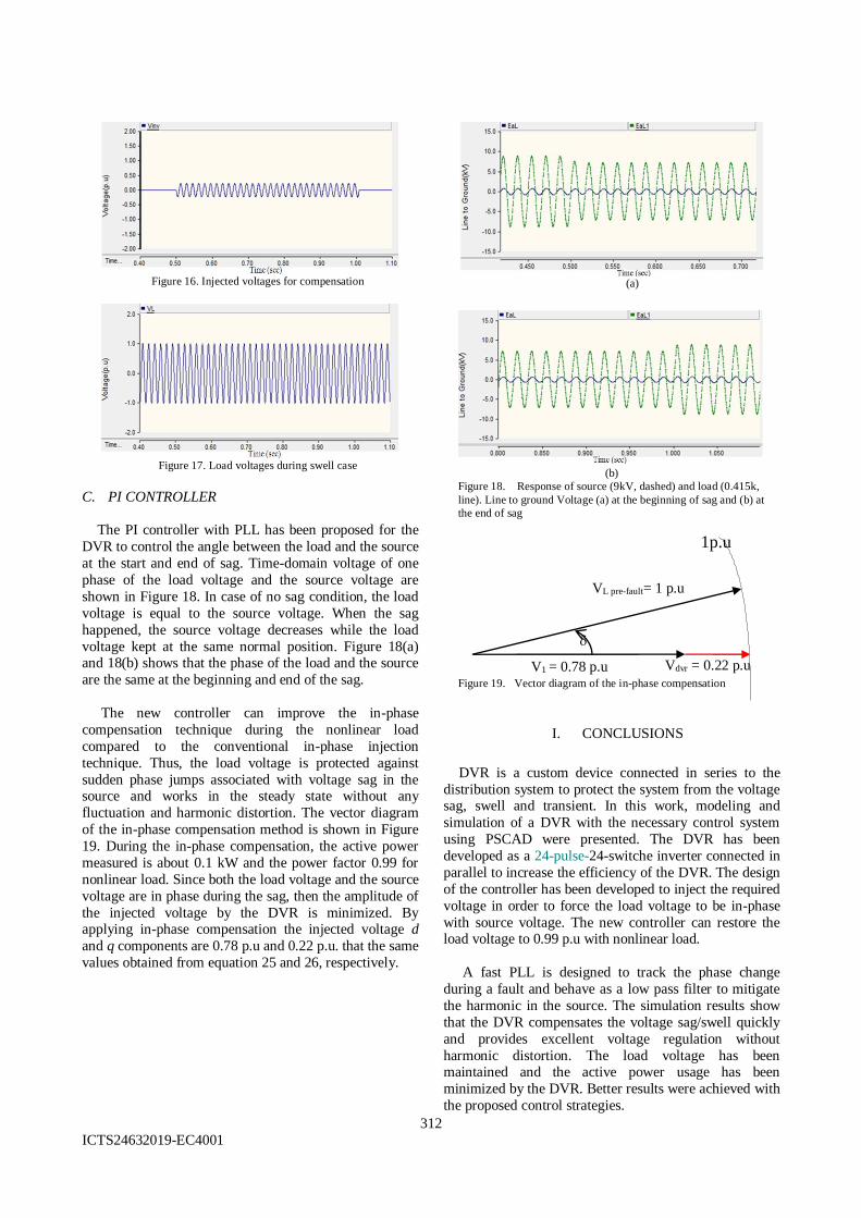
B. Voltage Swell Protection Mitigation
In case of voltage swell, the active power may be
drawn from the source into the ESC of the DVR. Figure
15 and 16 shows a voltage swell and compensated
voltage, respectively, where the voltage of the supply are
programmed to have 22% voltage swell. It can be noted
from Figure 17, the DVR can keep the load voltage
constant at all the measured cases.
Figure 15. Voltages swell with non-linear load
312
ICTS24632019-EC4001
1p.u
Vdvr = 0.22 p.u V1 = 0.78 p.u
VL pre-fault= 1 p.u
Figure 16. Injected voltages for compensation
Figure 17. Load voltages during swell case
C. PI CONTROLLER
The PI controller with PLL has been proposed for the
DVR to control the angle between the load and the source
at the start and end of sag. Time-domain voltage of one
phase of the load voltage and the source voltage are
shown in Figure 18. In case of no sag condition, the load
voltage is equal to the source voltage. When the sag
happened, the source voltage decreases while the load
voltage kept at the same normal position. Figure 18(a) and 18(b) shows that the phase of the load and the source
are the same at the beginning and end of the sag.
The new controller can improve the in-phase
compensation technique during the nonlinear load
compared to the conventional in-phase injection
technique. Thus, the load voltage is protected against
sudden phase jumps associated with voltage sag in the source and works in the steady state without any
fluctuation and harmonic distortion. The vector diagram
of the in-phase compensation method is shown in Figure
19. During the in-phase compensation, the active power
measured is about 0.1 kW and the power factor 0.99 for
nonlinear load. Since both the load voltage and the source
voltage are in phase during the sag, then the amplitude of
the injected voltage by the DVR is minimized. By applying in-phase compensation the injected voltage d
and q components are 0.78 p.u and 0.22 p.u. that the same
values obtained from equation 25 and 26, respectively.
(a)
(b)
Figure 18. Response of source (9kV, dashed) and load (0.415k,
line). Line to ground Voltage (a) at the beginning of sag and (b) at
the end of sag
Figure 19. Vector diagram of the in-phase compensation
I. CONCLUSIONS
DVR is a custom device connected in series to the
distribution system to protect the system from the voltage sag, swell and transient. In this work, modeling and
simulation of a DVR with the necessary control system
using PSCAD were presented. The DVR has been
developed as a 24-pulse-24-switche inverter connected in
parallel to increase the efficiency of the DVR. The design
of the controller has been developed to inject the required
voltage in order to force the load voltage to be in-phase
with source voltage. The new controller can restore the load voltage to 0.99 p.u with nonlinear load.
A fast PLL is designed to track the phase change
during a fault and behave as a low pass filter to mitigate
the harmonic in the source. The simulation results show
that the DVR compensates the voltage sag/swell quickly
and provides excellent voltage regulation without
harmonic distortion. The load voltage has been maintained and the active power usage has been
minimized by the DVR. Better results were achieved with
the proposed control strategies.

313
ICTS24632019-EC4001
The new method optimizes the system by injecting
small amount of active power during in-phase
compensation and tracks the supply voltage continuously
by using the two continuous-vector control algorithm as
compared to conventional method. From the results, it
can be seen that the two vector controller is effective in
tracking the phase, the harmonic and compensates the system within fast response time under various operating
condition such as non-linear load. Also the controller
design can charge the ESC by two directions by acting
like an AC-DC converter during normal operation and as
a DC-DC converter during disturbances. We concluded
that the 24-pulses-24-switches inverter and the new
controller have increased the performance of power
quality and kept the load voltage balanced and constant all the times.
REFERENCES
[1] A. de Almeida, L. Moreira, J. Delgado, “Design and
simulation of a novel self supported DVR for power quality improvement,” International journal of scientific and eng., vol.3, 2012.
[2] H. Math and J. Bollen, “Understanding power quality
problems: voltage sags and interruptions,” IEEE press, New York, 2000.
[3] M-M O. Antonio, O. Daniel, G. Miguel, A. O Fernando, j. Juan and de-la Rosa. Gonzalez. “Study of sag compensation with DVR,” IEEE Melecon: 990-993, 2006.
[4] Y. H. Chin and W. y. Horng, “Anew single phase active power filter with reduced energy storage capacitor,” IEEE 26th Annual Power Electronics Specialist Conference,vol 1: pp. 202-208, 1994.
[5] II-Y Chung, D-J. Won, S-Y. Park, S-II. Mooh and J-K. Park. The DC link energy control method in dynamic
voltage restorer system. International Journal of Electrical Power and Energy System, vol. 25 no.7, pp. 525-531, 2003.
[6] II-Y. Chung, S-Y. Park, S-I1. Moon and S-I1. Hur, “The control and analysis of zero sequence compensation in DVR system,” IEEE Power Engineering Society Winter Meeting. Vol. 3, pp.1021-1026, 2002.
[7] T. El- Shennawy. I, A. Moussa, A. El-Gammal, A. Mahmoud and A.Y. Abou-Ghazala, “A Dynamic voltage restorer for voltage sag mitigation in a refinery with induction motors loads,” American Journal of Engineering and Applied Science. Vol. 3, no.1, pp.144-151, 2010.
[8] H. Ezoji, Sheikholeslami, M. Rezanezhad, and H. Livan, “A new control method for dynamic voltage restorer with asymmetrical inverter legs based on fuzzy logic controller,” Simulation Modeling Practice and Theory. Vol. 18, no. 6, pp. 806-819, 2010.
[9] B. Ferdi, S. Benachaiba, S. Dib and R. Dehina, “Adaptive PI control of dynamic voltage restorer using fuzzy logic,” Journal of Electrical Engineering: Theory and Application. Vol. 4 no. 1, pp.165-173, 2010.
[10] A. Hilmy and B. Math, “Energy optimization techniques of static series compensator for constant power factor loads,”
IEEE Power Engineering Society. Vol. 1, no. 1, pp. 631-638, 2005.
[11] K. Hyosung and S. Seung-K, “Compensation voltage control in dynamic voltage restorer by use of feed forward and state feedback scheme,”IEEE Transaction on Power Electronic, Vol. 20, no. 5, pp. 1169-1177, 2005.
[12] G. N. John, and B. Freed, “A detailed compensation of system topologies for dynamic voltage restorers,” IEEE Transaction on Industry Applications, Vol.41, no.5, pp. 1272-1280, 2005.
[13] G. Joos, S. Chen, and L. Lopes, “Closed-loop state control of dynamic voltage restorer with fast compensation characteristics,” IEEE 39th IAS Annual Meeting
Conference, Vol. 4, no. 5, pp. 2252-2258, 2004. [14] M. N. Khaled, and M. Hasmaini, “Digital simulation of
uninterruptible power supply (UPS) and dynamic voltage restorer (DVR) for voltage sag mitigation,” (http://www.cs.uq.edu/~aupec/ aupec01/047_khald_AUPEC01. 2004.
[15] M. H. Rashid. Power Electronics Circuits, Devices and Applications, New Jersey: Prentice Hall. 1993, ch. 12, pp.
188-189.
[16] V. Jayalakshmi and N.O. Gunasekhari. “Dynamic voltage restorer using three phases AC-AC converters,” Journal of theoretical and applied information technology, Vol. 64, no.1, 2014.
BIOGRAPHIES
Ali Omar Al-Mathnani graduated with BSc from the Higher Institute
of Electronic, Libya in Electrical and Electronic Engineering in 1984.
Received MSc from University Putra Malaysia (UPM) in 2000. He got
PhD degree in Electrical Power Systems from the
University Kebangsaan Malaysia (UKM) in 2012. He
is currently lecturer in department of Electrical and
Electronics Engineering (EEE) at Sebha
University/Libya. His main research interests are in
power quality, power electronic device in power
system, VSI controller and intelligent system
development.
Ali Lesewed was born in Libya in 1963,
received his PhD in control Eng. and robotics
from Warsaw university. Currently is working
as associate professor at Zaitoona University -
Tarhoona, teaching control systems and
instrumentation, his interested in process
control, robotics and artificial intelligent
materials