Embed Size (px)
Citation preview
REDUCING THE POWER CONSUMPTION OF LEADING ONE DETECTOR CIRCUIT BY IMPLEMENTING
ITS DESIGN USING PASS TRANSISTOR LOGIC
K. Hari Kishore1, S. Fazal Noor Basha2, K. Vinny Ratnaja3, K. Karthik4, K. Deepak Kumar5
Department of ECE, K L University, Vaddeswaram, Guntur, A.P, India
Abstract: Power consumed by a VLSI device can be
reduced using pass transistor logic in the place of
CMOS logic. In general circuits at transistor level are
designed using CMOS logic where it takes more
number of transistors and also the complexity of the
circuit is very high . But pass transistor logic design
requires less number of transistors compared to CMOS
logic design while designing circuits at transistor level.
So, a leading one detector and a 1x2 De-multiplexer are
taken as an example and are implemented with the pass
transistor logic as well as CMOS logic and the
simulation results of these two designs are compared.
Schematic design for these circuits gives the number of
transistors used and layout gives the power analysis.
Keywords: LOD, CMOS, VLSI, Pass transistor, AND
gate, multiplexer, inverter, floating point, MSB, LSB,
NMOS and PMOS.
1. Introduction
Today we look for VLSI devices having low power
consumption and higher speed. Pass transistor logic is
one which paves way to attain these parameters. For
designing a logic gate such as AND gate which requires 6
transistors in CMOS logic but with pass transistor logic
we can implement the same with 2 transistors reducing
the power consumed by the remaining 4 transistors. Here
a leading-one detector(LOD) circuit is implemented with
this pass transistor logic. A LOD considers binary word
input traversing from MSB(most significant bit position)
to LSB(least significant bit position) in detection of the
first logic-1 bit, once detected it stops the process and
produces the output maintaining the length equal to the
input. There are 2-bit, 4-bit, 16-bit and 32-bit binary
word length LOD circuits, where the complexity of the
circuit is directly proportional to the input length. this
device's logic-circuit can be built using AND gates,
multiplexers and inverters. This LOD is mainly used in
the Floating point algorithm to normalise the integer and
fractional part.
2. Implementation
Figure2.1 represents a 2 bit leading one detector
schematic designed using the pass transistor logic. here
D0 and D1 are the inputs for the circuit, O0 and O1 are
the outputs from the circuit. A binary input '1 1' is given
to the circuit i.e. D0=1 as well as D1=1 and we get a
output of '1 0' i.e. O1=1 and O0=0 as the circuit detects
the leading one at the D1 position as it checks from
MSB(most significant bit) to LSB(least significant bit).
Figure 2.1. Circuit of 2-bit LOD
Figure 2.2. Layout of 2-bit LOD
As we can see in figure 2.2, the layout of the 2-bit
leading one detector represented in figure 1.3. the No.
of transistors are reduced as pass transistor logic is used
instead of CMOS logic where it take almost of 6
transistors pre logic gate(AND, OR etc).
3. Schematic design
A 4-bit leading one detector is also implemented
using the same pass transistor logic and it is tested using
a set of inputs. The power consumed by this circuit is
then compared with the power consumed by the same 4-
bit leading one detector which is designed using CMOS
logic.
International Journal of Pure and Applied MathematicsVolume 116 No. 23 2017, 561-566ISSN: 1311-8080 (printed version); ISSN: 1314-3395 (on-line version)url: http://www.ijpam.euSpecial Issue ijpam.eu
561
Figure 3.1. 4-bit LOD using pass transistor logic
Figure 3.2. 4-bit LOD using CMOS logic
In figure 3.1 we can see the 4-bit leading one
detector circuit which is designed using the pass
transistor logic. If input of '0110' given and when the
circuit traverses from MSB to LSB the leading one is
detected at the D2 position so, the O2 position of the
output gets high giving '0100'. In figure 3.2 the same 4-
bit leading one detector is implemented using CMOS
logic and the same input is applied. Though the outputs
of the two circuits are alike we can see that the number
of transistors required in Figure 3.2 are more when
compared to the one in figure 3.1. This increases the
overall power consumption and also the circuit
complexity is very high. So, minimum number of
transistors helps in reducing power consumption and
complexity of the circuit and this is attained by
designing it with pass transistor logic
4. Simulation Results
The power consumption of both the circuits i.e. 4-
bit leading one detector designed using pass transistor
logic and 4-bit leading one detector designed using
CMOS logic is compared using the simulation results
obtained for the schematics designs.
Figure 4.1. Output graph for the 4-bit LOD
using pass transistor logic
Figure 4.2. Output graph for the 4-bit LOD
using CMOS logic
Table 4.1. Comparison of power consumption
between the 4-bit LOD designed using pass transistor
logic and CMOS logic
Design Power consumed (micro
watts)
4-bit LOD designed using pass
transistor logic
9.578 micro watts
4-bit LOD designed using
CMOS logic
381.0 micro watts
From table 4.1 we can observe that the power
consumed by 4-bit LOD designed using pass
transistor logic is very less compared to that of the
CMOS logic.
Table 4.2. truth table for 4-bit LOD
Binary Input Binary Output
D3 D2 D1 D0 O3 O2 O1 O0
0 0 0 0 0 0 0 0
0 0 0 1 0 0 0 1
0 0 1 0 0 0 1 0
0 0 1 1 0 0 1 0
0 1 0 0 0 1 0 0
0 1 0 1 0 1 0 0
International Journal of Pure and Applied Mathematics Special Issue
562
0 1 1 0 0 1 0 0
0 1 1 1 0 1 0 0
1 0 0 0 1 0 0 0
1 0 0 1 1 0 0 0
1 0 1 0 1 0 0 0
1 0 1 1 1 0 0 0
1 1 0 0 1 0 0 0
1 1 0 1 1 0 0 0
1 1 1 0 1 0 0 0
1 1 1 1 1 0 0 0
Table 4.2 represents the truth table of 4-bit LOD with all
the possibilities i.e. all the 16 ways of inputs and their
respective outputs. D0, D1, D2 and D3 are the inputs
where as O0, O1, O2 and O3 are the outputs.
5. Further Implementation
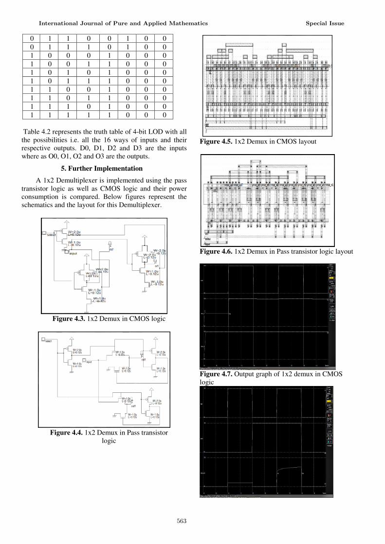
A 1x2 Demultiplexer is implemented using the pass
transistor logic as well as CMOS logic and their power
consumption is compared. Below figures represent the
schematics and the layout for this Demultiplexer.
Figure 4.3. 1x2 Demux in CMOS logic
Figure 4.4. 1x2 Demux in Pass transistor
logic
Figure 4.5. 1x2 Demux in CMOS layout
Figure 4.6. 1x2 Demux in Pass transistor logic layout
Figure 4.7. Output graph of 1x2 demux in CMOS
logic
International Journal of Pure and Applied Mathematics Special Issue
563
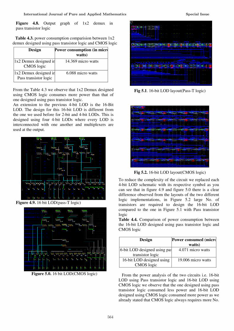
Figure 4.8. Output graph of 1x2 demux in
pass transistor logic
Table 4.3. power consumption comparision between 1x2
demux designed using pass transistor logic and CMOS logic
From the Table 4.3 we observe that 1x2 Demux designed
using CMOS logic consumes more power than that of
one designed using pass transistor logic.
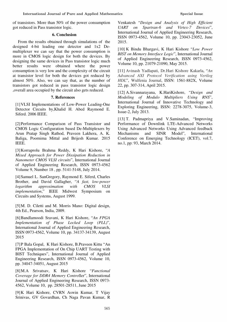
An extension to the previous 4-bit LOD is the 16-Bit
LOD. The design for this 16-bit LOD is different from
the one we used before for 2-bit and 4-bit LODs. This is
designed using four 4-bit LODs where every LOD is
interconnected with one another and multiplexers are
used at the output.
Figure 4.9. 16 bit LOD(pass-T logic)
Figure 5.0. 16 bit LOD(CMOS logic)
Fig 5.1. 16-bit LOD layout(Pass-T logic)
Fig 5.2. 16-bit LOD layout(CMOS logic)
To reduce the complexity of the circuit we replaced each
4-bit LOD schematic with its respective symbol as you
can see that in figure 4.9 and figure 5.0 there is a clear
difference observed from the layouts of the two different
logic implementations, in Figure 5.2 large No. of
transistors are required to design the 16-bit LOD
compared to the one in Figure 5.1 with Pass transistor
logic
Table 4.4. Comparison of power consumption between
the 16-bit LOD designed using pass transistor logic and
CMOS logic
Design Power consumed (micro
watts)
16-bit LOD designed using pass
transistor logic
4.071 micro watts
16-bit LOD designed using
CMOS logic
19.006 micro watts
From the power analysis of the two circuits i.e. 16-bit
LOD using Pass transistor logic and 16-bit LOD using
CMOS logic we observe that the one designed using pass
transistor logic consumed less power and 16-bit LOD
designed using CMOS logic consumed more power as we
already stated that CMOS logic always requires more No.
Design Power consumption (in micro
watts)
1x2 Demux designed in
CMOS logic
14.369 micro watts
1x2 Demux designed in
Pass transistor logic
6.088 micro watts
International Journal of Pure and Applied Mathematics Special Issue
564
of transistors. More than 50% of the power consumption
got reduced in Pass transistor logic.
6. Conclusion
From the results obtained through simulations of the
designed 4-bit leading one detector and 1x2 De-
multiplexer we can say that the power consumption is
more in CMOS logic design for both the devices. By
designing the same devices in Pass transistor logic much
better results were obtained where the power
consumption is very low and the complexity of the circuit
at transistor level for both the devices got reduced by
almost 50%. Also, we can say that, as the number of
transistors got reduced in pass transistor logic design
,overall area occupied by the circuit also gets reduced.
7. References
[1] VLSI Implementations of Low-Power Leading-One
Detector Circuits by,Khalid H. Abed Raymond E.
Siferd. 2006 IEEE.
[2] Performance Comparison of Pass Transistor and
CMOS Logic Configuration based De-Multiplexers by
Arun Pratap Singh Rathod, Praveen Lakhera, A. K.
Baliga, Poornima Mittal and Brijesh Kumar. 2015
IEEE.
[3] Korraprolu Brahma Reddy, K Hari Kishore, “A
Mixed Approach for Power Dissipation Reduction in
Nanometer CMOS VLSI circuits”, International Journal
of Applied Engineering Research, ISSN 0973-4562
Volume 9, Number 18 , pp. 5141-5148, July 2014.
[4] Samuel L. SanGregory, Raymond E. Siferd, Charles
Brother, and David Gallagher, “A fast, low-power
logarithm approximation with CMOS VLSI
implementation,” IEEE Midwest Symposium on
Circuits and Systems, August 1999.
[5] M. D. Ciletti and M. Morris Mano: Digital design,
4th Ed., Pearson, India, 2009.
[6] Bandlamoodi Sravani, K Hari Kishore, “An FPGA
Implementation of Phase Locked Loop (PLL)”,
International Journal of Applied Engineering Research,
ISSN 0973-4562, Volume 10, pp. 34137-34139, August
2015
[7] P Bala Gopal, K Hari Kishore, B.Praveen Kittu “An
FPGA Implementation of On Chip UART Testing with
BIST Techniques”, International Journal of Applied
Engineering Research, ISSN 0973-4562, Volume 10,
pp. 34047-34051, August 2015
[8] M.A Srivatsav, K Hari Kishore “Functional
Coverage for DDR4 Memory Controller”, International
Journal of Applied Engineering Research, ISSN 0973-
4562, Volume 10, pp. 28501-28511, June 2015
[9] K Hari Kishore, CVRN Aswin Kumar, T Vijay
Srinivas, GV Govardhan, Ch Naga Pavan Kumar, R
Venkatesh “Design and Analysis of High Efficient
UART on Spartran-6 and Virtex-7 Devices”,
International Journal of Applied Engineering Research,
ISSN 0973-4562, Volume 10, pp. 23043-23052, June
2015.
[10] K Bindu Bhargavi, K Hari Kishore “Low Power
BIST on Memory Interface Logic”, International Journal
of Applied Engineering Research, ISSN 0973-4562,
Volume 10, pp. 21079-21090, May 2015.
[11] Avinash Yadlapati, Dr.Hari Kishore Kakarla, “An
Advanced AXI Protocol Verification using Verilog
HDL”, Wulfenia Journal, ISSN: 1561-882X, Volume
22, pp. 307-314, April 2015.
[12] A.Sivannarayana, K.HariKishore, “Design and
Modeling of Modulo Multipliers Using RNS”,
International Journal of Innovative Technology and
Exploring Engineering, ISSN: 2278-3075, Volume-3,
Issue-2, July 2013.
[13] T. Padmapriya and V.Saminadan, “Improving
Performance of Downlink LTE-Advanced Networks
Using Advanced Networks Using Advanced feedback
Mechanisms and SINR Model”, International
Conference on Emerging Technology (ICET), vol.7,
no.1, pp: 93, March 2014.
International Journal of Pure and Applied Mathematics Special Issue
565

566