Embed Size (px)
Citation preview
1IntroductionHiroshi Ishikawa
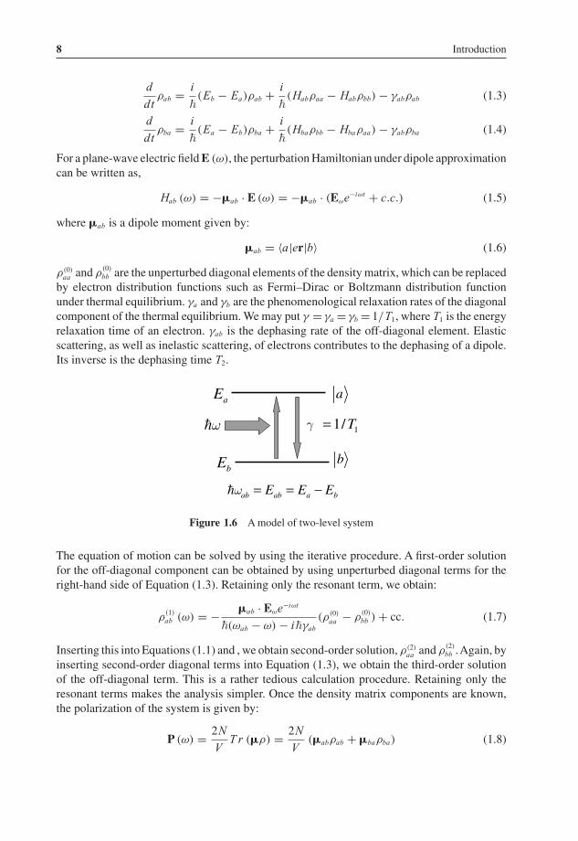
1.1 Evolution of Optical Communication Systems and DeviceTechnologies
Deployment of the optical communication systems started at the end of 1970s. The bit rate of theearly-stage systems was 100 Mb/s (1980), increasing to 400 Mb/s, 565 Mb/s, 1.6 Gb/s, 2.4 Gb/sand 10 Gb/s over the past three decades. Increasing the transmission capacity was achieved notjust by increasing the bit rates as wavelength division multiplexing (WDM) technology wasdeveloped in the 1990s. Systems capable of 100–200 wavelengths multiplexing with a singlechannel bit rate of 2.4 Gb/s and 10 Gb/s were deployed, having scalable total capacities up to2 Tb/s. Recently, deployments of WDM systems with a single channel bit rate of 40 Gb/s havestarted. Looking into the future, we will be required to realize still larger capacity networks,as will be discussed later.
Owing to the above-mentioned increase in transmission capacity, broadband Internet net-work systems have come to be used widely since we entered Twenty-first century. Internetprotocols (IP), various browsing technologies, varieties of related software, and increasedperformance of personal computers and routers, largely contributed to the spread of broad-band networks, which have had a huge impact on our society and our daily life. Worldwidee-commerce and e-business has become an essential part of our economy with outsourcing ofoffice jobs, research and development being done using networks. Even production at remotesites is becoming possible though networks. The world-wide impact of broadband networks isclearly described in such books as Revolutionary Wealth by Alvin Toffler and Heidi Toffler[1],and The World is Flat by Thomas L. Friedman[2].
When we looked back the technological evolution of these networks, development of newor higher performance devices and components played crucial roles. Such devices were low-loss optical fibers, semiconductor lasers, detectors such as APDs (avalanche photodiodes) andPIN photodiodes, integrated driver circuits, multiplexing and demultiplexing ICs, and fiber
Ultrafast All-Optical Signal Processing Devices Edited by Hiroshi Ishikawac© 2008 John Wiley & Sons, Ltd
COPYRIG
HTED M
ATERIAL
2 Introduction
amplifiers. Many passive components such as arrayed waveguide gratings (AWG) and opticalfilters were needed for WDM systems.
We can see a good example in light sources showing how their innovation contributed toan increase in transmission bit rates. First, Fabry-Perot lasers, which lased in multiple spectraenabled transmission rates of up to 400 Mb/s. To increase the bit rate to more than 1 Gb/s,lasers with single wavelengths were essential to minimize the effect of chromatic disper-sion of fiber. Distributed feedback (DFB) lasers were developed to this end. For longer-spantransmission with bit rates above 10 Gb/s, wavelength chirp in a single lasing spectrum wasa problem. Then the external modulation scheme was developed. Electro-optic modulatorsusing LiNbO3, semiconductor-based, electro-absorption modulators (EAM) were developed.Monolithic integration of DFB laser and EAM was done to realize a compact light source.Owing to these advances in light sources together with advances in other devices and techno-logies, it was possible to increase the transmission bit rate. If we target much higher bit ratesystems, such as 100 Gb/s and 1 Tb/s, for future applications, the key will be the developmentof new and higher performance devices as well.
1.2 Increasing Communication Traffic and Power Consumption
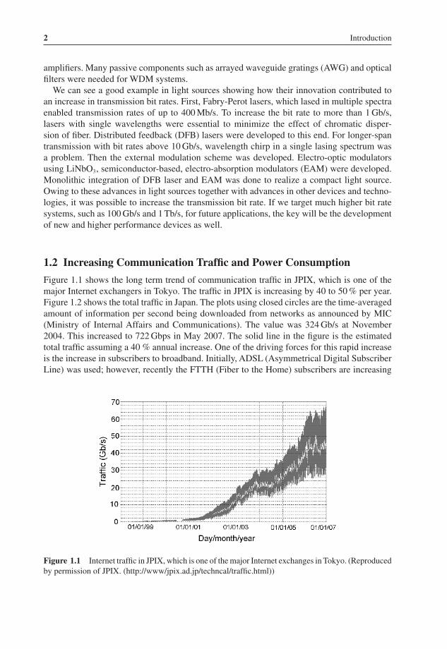
Figure 1.1 shows the long term trend of communication traffic in JPIX, which is one of themajor Internet exchangers in Tokyo. The traffic in JPIX is increasing by 40 to 50 % per year.Figure 1.2 shows the total traffic in Japan. The plots using closed circles are the time-averagedamount of information per second being downloaded from networks as announced by MIC(Ministry of Internal Affairs and Communications). The value was 324 Gb/s at November2004. This increased to 722 Gbps in May 2007. The solid line in the figure is the estimatedtotal traffic assuming a 40 % annual increase. One of the driving forces for this rapid increaseis the increase in subscribers to broadband. Initially, ADSL (Asymmetrical Digital SubscriberLine) was used; however, recently the FTTH (Fiber to the Home) subscribers are increasing
Figure 1.1 Internet traffic in JPIX, which is one of the major Internet exchanges in Tokyo. (Reproducedby permission of JPIX. (http://www/jpix.ad.jp/techncal/traffic.html))

Increasing Communication Traffic and Power Consumption 3
Nov.1998
Nov.2000
Nov.2002
Nov.2010
Nov.2008
Nov.2012
Nov.2004
Nov.2006
FT
TH
sub
scrib
ers
(mill
ion)
Inte
rnet
traf
fic (
Tbp
s)
2.5
2.0
1.5
1.0
0.5
25
20
15
10
5324Gbps (Nov. 2004)
468Gbps (Nov. 2005)
637Gbps (Nov. 2006.)
722Gbps (May 2007)
FTTH subscriber~25million (2010)
Figure 1.2 Total traffic in Japan. Solid circles are evaluated value by Ministry of Internal Affairs andCommunications. The line is the fit assuming a 40 % annual increase. Bars show the subscribers to FTTH
rapidly. NTT, one of the major carrier companies in Japan, is aiming at 20 million subscribersto FTTH by 2010. The bars in Fig. 1.2 are subscribers to FTTH. NTT is to bring NGN (NextGeneration Network) into service in 2008. NGN is an IP-based network enabling variousservices with higher quality [3].
The dramatic increase in traffic and the plan to increase various services will cause a seriousproblem, namely the power consumption of the network equipment. Figure 1.3 shows therouter power consumption in Japan as estimated by T. Hasama of AIST (National Institute ofAdvanced Industrial Science and Technology). The power consumption in 2001 is based onactual data. Assuming a 40 % annual increase in traffic and reduction of the CMOS-LSI drivevoltage, plotted as closed circles in the figure, the power consumption of routers will reach6.4 % of the total power generation in 2020 even for the low CMOS-LSI drive voltage of 0.8 V.If the drive voltage reduction of CMOS-LSI is insufficient, the power consumption will stilleasily reach a few tens of a percentage point or more. This means we cannot have the benefitsof larger capacity networks.
One of the causes of large power consumption in the present network is the WDM schemeand electrical routing of the packet signals. The WDM requires O/E (optical to electrical)signal and E/O (electrical to optical) signal conversion circuits with the same number as thatof the wavelength, resulting in an increase in power consumption. In addition to this, electricalsignal processing for IP packet routing and switching at the router consumes large amountsof power. If we could realize 100 Gb/s to 1 Tb/s bit-rate transmission, huge capacity datacould be transmitted with a small number of wavelengths, which might reduce the powerconsumption. If we could process ultrafast signals without converting to electrical signals,this would also reduce the power consumption of routers. Consequently, the development ofultrafast all-optical devices is very important for future, low power-consumption huge capacitynetworks

4 Introduction
0
100
200
300
400
500VLSI
600
700
2001 2006 2010 2015 2020
6.4%
4.7%
1.9%0.8%
0.08%0
1
2
3
4
5
6
7
Year
Pow
er c
onsu
mpt
ion
× 1
08 (k
Wh/
year
)
Ass
umed
LS
I der
ive
volta
ge (
V)
Figure 1.3 Estimated power consumption by Internet routers in Japan. Original data is from T. Hasamaof AIST. The value for 2001 is actual data. Plots shown by solid circles are the assumed drive of LSIvoltage used in routers. The percentages in the figure are the proportion of total power generation. Ifwe assume a 40 % increase in traffic, the router power consumption reaches 6.4 % of the total powergeneration in 2020 even for a low LSI drive voltage of 0.8 V
1.3 Future Networks and Technologies
1.3.1 Future Networks
Forecasting the future of networking is of large importance in planning research and devel-opment. It is obvious that the traffic of video content will keep on increasing. At present,a large proportion of the network bandwidth is occupied by video content, such as TV andmovies, and moving-picture distribution services. The convergence of broadcasting and com-munication will soon take place in NGN (Next Generation Network). Network users willrequire higher resolution pictures; however there is a limitation on resolution due to the lim-ited bandwidth. International distribution of 4K-digital cinema (for resolution of 2000 × 4000,the required bandwidth is above 6 Gb/s without compression) by network was demonstratedusing data compression by JPEG2000 [4]. NHK (the Japanese public broadcasting organiz-ation) is developing ultra-HDTV (high definition TV) having a resolution of 4320 × 7680,requiring a bandwidth of 72 Gb/s, and is planing to start broadcasting ultra-HDTV in 2025 [5].
If we could get rid of the bandwidth limitation, there would arise a lot of new applications.Higher resolution, real-time, moving pictures with realistic sound will make the TV conferencea far more useful tool. International conferences could even be held using remote-presencetechnology. This would reduce the energy consumption by reducing the traffic. Medical applic-ations for the network will also be important. Using high-resolution pictures without time delay,remote diagnosis can be done, and even remote surgery is within its scope. Other important asso-ciated technology would be grid technology. One of the present applications of grid technologyis to establish connections or paths between various computer sites or data storages. The largebandwidth optical paths, which can be controlled by a user, will enable high performance grid

Future Networks and Technologies 5
computing (e-science) by connecting computers worldwide. Grid-based virtual huge capa-city storage, and grid-based economy (e-economy, e-commerce, e-production) will also beimportant issues.
When we look at the current IP-based network, it is not suited to handling such a hugecapacity of data. It is optimized rather to low granularity traffic and requires data compressionfor large-capacity data because of the bandwidth limitation. This causes the time delay, andwe cannot obtain the benefit of real-time information. A novel network capable of real-time,high-capacity, transmission is required. One candidate is the optical-path network, in whichend-to-end connection and broadcasting end to multi-ends connection can be achieved withoptical paths where large-scale optical switches are used for routing. The concept of opticalpath has been discussed in terms of wavelength path or virtual wavelength path [6]. Thedynamic huge-scale path network including the wavelength path with very high bit rate ishighly attractive as a future network for huge capacity data transmission. In such path systems,information can be transmitted transparently, i.e. regardless of the modulation format and bitrate, without using electronic routers. Combination of IP based networks, which handle smallgranularity data, and dynamic optical path networks, which handle huge capacity data withvery high bit rates, is one of the promising forms of the future network.
1.3.2 Schemes for Huge Capacity Transmission
There are two ways of achieving huge capacity transmission. One is the optical time divisionmultiplexing (OTDM) technology as illustrated in Figure 1.4, and the other is the employmentof multilevel modulation schemes as illustrated by Figure 1.5.
Figure 1.4 Optical time division multiplexing (OTDM) scheme. (a) By giving proper delay to eachchannel we can generate a very fast optical signal. (b) For demultiplexing we are required to developall-optical switches

6 Introduction
8PSK 16QAMOOK
Im(E) Im(E) Im(E)
Re(E)Re(E) Re(E)θ
Figure 1.5 Constellation diagram of OOK (on–off keying), 8 PSK (phase shift keying) and 16 (quad-rature amplitude modulation). By utilizing phases of light waves we can realize multilevel modulation
In the OTDM scheme, optical signals from different channels are multiplexed by applying aproper delay to each channel in order to get high bit-rate signals. We can generate high bitrates, for example 160 Gb/s or 1.28 Tb/s [7], which cannot be achieved by electric circuits.To make the OTDM systems into real ones, we need to develop ultrafast, all-optical signalprocessing devices. There are ultrafast light sources and ultrafast all-optical gate switchesfor such functions as gating, clock extraction, 2R (retiming and reshaping) operations, andDEMUX (demultiplexing). To make the system flexible, a wavelength conversion device isalso essential. Dispersion compensation including polarization-mode dispersion, is also animportant issue for long-distance transmission.
The other scheme involves the use of multilevel modulation, which not only uses theamplitude of light but also the phase [8, 9]. By utilizing phases of the light field we canperform multilevel modulation. Figure 1.5 shows examples of multilevel modulation inthe form of constellation mapping. The horizontal axis is the real part of the electric fieldand the vertical axis is the imaginary part. Figure 1.5(a) is the conventional on–off key-ing (OOK). Figure 1.5(b) is 8 PSK (phase shift keying), which can transmit 3 bit/symbol,and (c) is 16 QAM (quadrature amplitude modulation) capable of 4 bit/symbol modulation.Precise control of phases and sophisticated decoding technology are required to realize alarge multilevel [10, 11]. The multilevel scheme has an advantage in that it can increase thetotal capacity without increasing the symbol rate. This makes the dispersion compensationeasier.
1.4 Ultrafast All-Optical Signal Processing Devices
1.4.1 Challenges
In this book we describe the challenges for semiconductor-based ultrafast (100 Gb/s - 1 Tb/s)all-optical signal processing devices. A major application is in ultrafast OTDM networks;however, a multi-level scheme based on a symbol rate beyond 100 Gb/s could also be a possib-ility in further increasing the transmission rate. Focus is put on semiconductor-based devices,although fiber-based devices are used for ultrafast OTDM experiments, for example, NOLM(Nonlinear Optical Loop Mirror) [12, 13]. Advantages of semiconductor devices when com-pared with fiber devices are their small size and possible integration of devices for higherfunctionality. With semiconductor devices, however, there is a lot of difficulties in realizingpractical devices. One of the major difficulties is the intrinsic one that faster all-optical device

Ultrafast All-Optical Signal Processing Devices 7
operation based on optical nonlinearity requires larger optical energy. This is theoreticallyillustrated in the next section. This problem can be avoided in fiber devices because long fiber-lengths can be used to obtain sufficient nonlinearity for low energy operation. In semiconductordevices, although the nonlinear susceptibility is greater than with optical fibers, device sizesare very small. It is not, therefore, easy to realize low-energy operating devices; hence, for thedevelopment of ultrafast all-optical semiconductor devices, full utilization of many new ideasand concepts are required.
A systematic challenge for semiconductor-based, ultrafast all-optical devices was TheFemtosecond Technology Project (1995–2004) in Japan, which was conducted with the sup-port of the Ministry of Trade and Industry, and NEDO (New Energy and Industrial TechnologyDevelopment Organization) [14]. Mode-locked semiconductor lasers were developed, as werevarious types of all-optical gate switches, and WDM transmission technology based on 160Gb/s–320 Gb/s OTDM signals. Described in this book are mode-locked lasers (Chapter 2),symmetric Mach–Zehnder gate switch (Chapter 3), intersub-band transition gate switches(Chapter 5), four-wave mixing wavelength converters (Chapter 6), and transmission techno-logies (Chapter 7). Another project, named ‘Research and Development on Ultrahigh-speedBackbone Photonic Network Technologies’ (1996–2005) was conducted under the auspicesof NICT (National Institute of Information and Communication Technology). In this project,a 160-Gb/s CS-RZ (carrier suppressed return to zero) signal was generated by OTDM tech-nology using an electro-absorption modulator (EAM) [15]. A field transmission experimentwas demonstrated over 635 km. The OTDM light source developed in this project is describedin Chapter 2, and the transmission experiment is briefly reviewed in Chapter 7. Outside ofthese projects, much interesting research work has been done worldwide, including a deviceusing an ultrafast photodiode and traveling-wave electro-absorption modulator, described inChapter 4, and a use of SOA with wavelength filter enabling use of only the very fast responsecomponent of SOA response (Chapter 3).
1.4.2 Basics of the Nonlinear Optical Process
For ultrafast, all-optical, signal processing using semiconductor-based devices, we use opticalnonlinear effects, mainly the third-order nonlinearity. The third-order process is highly usefulsince it gives such effects as absorption saturation (gain saturation) and four-wave mixing.Here we briefly look at the third-order nonlinear process, taking the simplest two-level systemas an example in order to achieve basic understanding of the device operation and to illustratethe intrinsic difficulty with all-optical ultrafast devices.
Figure 1.6 shows a two-level system. We assume N two-level systems with inversion sym-metry in a volume V . We consider a case where only one frequency plane wave with angularfrequency ω is applied. The response of the two-level system to the optical field can be describedby a density matrix equation of motion [18, 19]. If we write down all the components of theequation of motion:
d
dtρaa = i
�(ρabHba − Habρba) − γa
(ρaa − ρ(0)
aa
)(1.1)
d
dtρbb = i
�(ρbaHab − Hbaρab) − γb
(ρbb − ρ
(0)
bb
)(1.2)
8 Introduction
d
dtρab = i
�(Eb − Ea)ρab + i
�(Habρaa − Habρbb) − γabρab (1.3)
d
dtρba = i
�(Ea − Eb)ρba + i
�(Hbaρbb − Hbaρaa) − γabρba (1.4)
For a plane-wave electric field E (ω), the perturbation Hamiltonian under dipole approximationcan be written as,
Hab (ω) = −�ab · E (ω) = −�ab · (Eωe−iωt + c.c.) (1.5)
where �ab is a dipole moment given by:
�ab = 〈a|er|b〉 (1.6)
ρ(0)aa
and ρ(0)
bb are the unperturbed diagonal elements of the density matrix, which can be replacedby electron distribution functions such as Fermi–Dirac or Boltzmann distribution functionunder thermal equilibrium. γa and γb are the phenomenological relaxation rates of the diagonalcomponent of the thermal equilibrium. We may put γ = γa = γb = 1/T1, where T1 is the energyrelaxation time of an electron. γab is the dephasing rate of the off-diagonal element. Elasticscattering, as well as inelastic scattering, of electrons contributes to the dephasing of a dipole.Its inverse is the dephasing time T2.
11/Tγ =
a
bbE
aE
ab ab a bE E Eω = = −�
ω�
Figure 1.6 A model of two-level system
The equation of motion can be solved by using the iterative procedure. A first-order solutionfor the off-diagonal component can be obtained by using unperturbed diagonal terms for theright-hand side of Equation (1.3). Retaining only the resonant term, we obtain:
ρ(1)
ab (ω) = − �ab · Eωe−iωt
�(ωab − ω) − i�γab
(ρ(0)
aa− ρ
(0)
bb ) + cc. (1.7)
Inserting this into Equations (1.1) and , we obtain second-order solution, ρ(2)aa
and ρ(2)
bb .Again, byinserting second-order diagonal terms into Equation (1.3), we obtain the third-order solutionof the off-diagonal term. This is a rather tedious calculation procedure. Retaining only theresonant terms makes the analysis simpler. Once the density matrix components are known,the polarization of the system is given by:
P (ω) = 2N
VT r (�ρ) = 2N
V(�abρab + �baρba) (1.8)

Ultrafast All-Optical Signal Processing Devices 9
The first-order solution of the off-diagonal terms gives the first-order polarization, and the third-order off-diagonal terms give the third-order polarization. Retaining the first- to the third-orderterms, the generated polarization can be written as:
P (ω) = ε0
(χ(1) (ω) + χ(3) (ω) |Eω|2
)Eω (1.9)
where ε0 is the vacuum dielectric constant, χ(1) is linear susceptibility and χ(3) is the third-order nonlinear susceptibility. There is no second-order nonlinearity because we have assumeda system with inversion symmetry. The above iterative solutions of the equation of motion givesusceptibilities as:
χ(1) (ω) = −2N |μab|2
ε0V
1
�(ωab − ω) − i�γab
(ρ(0)
aa− ρ
(0)
bb ) (1.10)
χ(3) (ω) = − 8N |μab|4γab(ρ(0)aa
− ρ(0)
bb )
ε0V γ (�ω − �ωab + i�γab)(�2(ωab − ω)2 + �2γ 2
ab
) (1.11)
Development of a light electric field under nonlinear susceptibility can be written using slowlyvarying envelope approximation as:
d
dzEω = − 1
2ik
(ε0μ0ω
2 + ε0μ0ω2pχ(1) − k2
)Eω − 1
2ikε0μ0ω
2χ(3)|Eω|2Eω (1.12)
where μ0 is the vacuum permeability. This can be rewritten by separating the real and imaginarypart of the susceptibility as:
d
dzEω = i
2kε0μ0ω
2
[1 + χ
(1)
R + χ(3)
R |Eω|2 − k2
ε0μ0ω2
]Eω − 1
2kμ0ε0ω
2(χ
(1)
I + χ(3)
I |Eω|2)
Eω
(1.13)
Suffix R denotes the real part, and I denotes the imaginary part. For this equation to hold:
k2 = ε0μ0ω2(1 + χ
(1)
R + χ(3)
R |Eω|2)
(1.14)
d
dzEω = − ω
2cn
(χ
(1)
I + χ(3)
I |Eω|2)
Eω (1.15)
Equation (1.14) gives the refractive index as:
n = (1 + χ
(1)
R + χ(3)
R |Eω|2)1/2
(1.16)
This equation means that the refractive index changes in the optical field through a third-ordernonlinear process. Equation (1.15) can be rewritten as an equation describing optical powerpropagation. Using:
d
dz|Eω|2 = E∗
ω
dEω
dz+ E
dE∗ω
dz(1.17)
|Eω|2 = 2Z0
nP (1.18)

10 Introduction
where P is the optical power density and Z0 is the vacuum impedance given by:
Z0 =√
μ0
ε0
(1.19)
We can obtain the equation for the optical power density as:
dP
dz= − α0P
1 − Z0χ(3)
I
2nχ(1)
I
= − α0P
1 + P
Ps
(1.20)
where α0 is the linear absorption coefficient and is expressed as:
α0 = ω
cnχ
(1)
I =(
2N
V
)Z0ωμ2
ab
n
�γab
�2 (ωab − ω)2 + �2γ 2
ab
�ρ(0) (1.21)
where �ρ(0) = ρ(0)
bb − ρ(0)aa
and Ps is:
Ps (ω) = −2nχ(1)
I
Z0χ(3)
I
= cnε0γ
2μ2abγab
(�
2 (ωab − ω)2 + �
2γ 2ab
)(1.22)
Equation (1.20) means that the absorption coefficient is reduced for large optical power densityand is half of the initial value for P = Ps . Ps is called the saturation power density and we canuse this for an all-optical gate. If we introduce an intense control pulse to the two-level system,the system becomes transparent by absorption saturation. Under this condition, a weak signallight can pass through the two-level system. This is the ‘on state’ of the gate. When we turnoff the control pulse, the system is again absorptive with a time constant of T1, and the gateswitch is in the ‘off-state’. It can be seen that the absorption saturation takes place over thehomogenous width of �ω = ω − ωab = �γab. When there is population inversion, the two-levelsystem has optical gain, and the third order process gives the gain saturation. SOA correspondsto this case. This also can be used as an all-optical gate switch.
To examine the relationship between the response speed and the optical power densityneeded to saturate the two-level system, we consider the on resonant case, i.e. ω = ωab. Thesaturation power density is given by:
Ps = n�2γ γab
2μ2abZ0
= cnε0�2
2μ2abT1T2
(1.23)
The smaller T1 and T2 give faster response speeds while, however, smaller T1 and T2 givelarger Ps . Large optical energy is needed for a very fast nonlinear response. This is the intrinsiclimitation in using nonlinearity for all-optical signal processing devices. In the evaluation ofultrafast devices, we use short pulses. It is customary to use pulse energy rather than opticalpower density as a measure of device performance. The saturation pulse energy is the productof Ps, the cross section of the beam, and the pulse width. The discussion on the relationshipbetween the response speed and optical power density (pulse energy) also holds for the refract-ive index, because of Kramers–Kronig relation that connects the absorption coefficient andrefractive index.

Overview of the Devices and Their Concepts 11
More detailed analysis reveals that there are varieties of interesting effects in the opticalnonlinearity. For example, if we assume pump wave ωp and signal wave ωs of different fre-quencies and consider beat frequency 2ωp − ωs , we obtain the third-order susceptibility fornondegenerate four-wave mixing. This frequency is the beat frequency between ωp − ωs andωp, i.e. the pump wave ωp is scattered by the beat frequency ωp − ωs to generate a new fre-quency 2ωp − ωs . Detailed discussion on four-wave mixing in SOA is described in Chapter 6,which considers some other effects on the third-order nonlinear susceptibility. If we furtherextend the analysis to multi-level systems, we obtain expressions for multi-photon absorptionand Raman scattering processes [17].
To extend the analysis from the simple two-level system to semiconductor band structures,following substitution using the wave number of electrons, k applies.
(2N
V
)→ D (k) dk, where D (k) is the density of state.
Express parameters in terms of k, for example �ωi → �2k2
i
2m∗ , where m∗ is the electron effectivemass:
ρ(0)
aa, ρ
(0)
bb → Fermi–Dirac distribution function expressed in terms of k
Then integrate over k. This gives the parameters for semiconductor-based systems. It goeswithout saying that relationship (1.23) also holds for semiconductors.
1.5 Overview of the Devices and Their Concepts
Here we briefly review the devices described in this book in order to have an overview oftheir basic concepts as related to ultrafast operation. Lots of new ideas are employed and newchallenges have arisen.
In Chapter 2, we describe ultrafast light sources. These are mode-lock lasers and EAM-basedlight sources. The mode-locked laser uses the absorption-saturation effect for mode locking.Hybrid mode locking using microwave modulation and sub-harmonic synchronous lockingwere employed to generate high repletion rate short pulses with small jitter. Mode-lockedlasers can also be used for clock extraction from the deteriorated received signal. The 3R(retiming, retiming, regeneration) operation for a 160-Gb/s signal was demonstrated usingmode-locked lasers. Also described in Chapter 2 is the EAM-based ultrafast light source. Bycascading two EAMs, which are modulated by a 40-Gb/s electric signal, 3-ps width shortpulses with 40 Gb/s repletion were generated. Then, a 160 Gb/s optical signal was generatedby OTDM, i.e. by applying a proper time delay to four 40-Gb/s channels using space optics. Aninteresting point was that the CS-RZ (carrier suppressed return to zero) signal at 160 Gb/s wasgenerated by controlling the phases of each channel by temperature. The CS-RZ modulationformat is robust to nonlinear effect in the fiber, such as four-wave mixing, because of no carrierin the spectrum.
In Chapter 3, switching using a SOA (semiconductor optical amplifier) is discussed. In theSOA, population inversion is realized by current injection. When we put in an intense gatepulse, it causes a gain reduction and an associated refractive index change takes place. This isthe third-order nonlinear process, and its basic principle can be understood by replacing theabsorption coefficient in Equation (1.20) by the gain of SOA. A characteristic feature of this

12 Introduction
response is that it is very fast for the rise time; however, there is a slow component of the orderof 1ns in the response recovery, which is the band-to-band recombination lifetime. This slowcomponent has been the obstacle in realizing ultrafast switching devices above 100 Gb/s. Twomethods are described for solving this problem. One is to use a wavelength filter to selectonly the very fast, blue-shifted component of the response [16, 17]. By using only the fastcomponent, which is due to intraband electron–phonon scattering, we can perform wavelengthconversion, 2R (retiming and reshaping) operation and DEMUX operation. Another methodis to use the Symmetric Mach-Zehnder (SMZ) interferometer configuration. By putting SOAsymmetrically at both arms of a SMZ, we can cancel out the slow response component by usinggate on pulse and off pulse. Using the SMZ configuration, DEMUX operation of 640 Gb/s to10 Gb/s was demonstrated. Error free DEMUX operations of 320 to 40 Gb/s and to 10 Gb/swere also demonstrated. Also demonstrated were the wavelength conversion and retiming andreshaping (2R) operations. It is interesting that this SMZ gate switch can be used for ratherslow signal processing. Bit rate free 2R operation (2.5–42 Gb/s) was demonstrated for NRZsignals.
Chapter 4 describes a different approach to realizing ultrafast signal processing. The Uni-Traveling-Carrier Photodiode (UTC-PD), which has a very fast response with high outputcurrent, followed by a monolithically integrated traveling-wave electro-absorption modulator(TW-EAM), was used for ultrafast signal processing. In this method, very short gate pulses areconverted to the electrical signal using UTC-PD, which has a 3-dB cut-off frequency of above300 GHz. The electric signal modulates the optical signal by TW-EAM, which is monolithicallyintegrated with the UTC-PD. Using this method, DEMUX operation of 320 Gb/s to 10 Gb/swas demonstrated. We are not bothered by the intrinsic relationship of response time and energyrequirement inherent to the third-order nonlinear process. Careful design taking into accountRC limit and phase matching of the traveling wave EAM modulator are crucial issues.
Chapter 5 describes the inter-sub-band transition (ISBT) gate. The ISBT gate utilizes theabsorption saturation in the inter-sub-band transition in the conduction band of a very thinquantum well. To obtain a 1.55 �m transition, a deep potential well and ultra-thin wellhave to be employed. Material systems satisfying this are (GaN)/AlN, (CdS/ZnSe)/BeTe,and (InGaAs)/AlAs/AlAsSb material systems. Materials in parentheses are well layer mater-ials. Response time depends on T1 and T2 times, which depend on parameters such asLO-Phonon energy, effective mass, and dielectric constant. Because of these paramet-ers the (GaN)/AlN quantum well shows the fastest response, then (CdS/ZnSe)/BeTe, withthe (InGaAs)/AlAs/AlAsSb system being the slowest. However, even in the slowest case, theresponse time is about 1 ps. Owing to the very fast response time of ISBT, we can realize avery fast absorption saturation type gate. A problem, however, is that gating energy becomeslarge for a fast response, as can be seen from Equation (1.23). Then in ISBT gates, much efforthas been put into realizing low-gating energy despite the very fast response. In addition to theintensity gate based on absorption saturation, a new very interesting phenomenon has beenfound in the InGaAs/AlAs/AlAsSb ISBT gate, i.e all-optical, deep-phase modulation can beused on the loss-less TE mode probe light when the quantum well is illuminated by a TM gatepulse. This new phenomenon is quite useful, and wavelength conversion of picosecond pulseswith 10 Gb/s repetition was demonstrated using this effect.
In Chapter 6, four-wave mixing (FWM) wavelength conversion using SOA is presented.Various methods of wavelength conversion are reviewed and then the chapter focuses on FWMusing the semiconductor gain medium, SOA and semiconductor lasers. Various effects giving
References 13
third-order nonlinear susceptibility are discussed. These are carrier density pulsation, carrierheating, and spectral hole burning.An impeding effect for the application of FWM for practicalsystems is the asymmetry in the wavelength conversion efficiency with respect to the pumpingwavelength. The wavelength conversion efficiency from long wavelength to short wavelengthis high, while the short to long is small. To solve this problem, quantum dot SOA was used,and almost symmetric wavelength conversion was demonstrated at 1.3 �m. The wavelengthconversion of a 160-Gb/s signal was demonstrated at 1.55 �m, although there remained asym-metry. Also demonstrated was the use of a two-wave pumping scheme using bulk active layerSOA monolithically integrated with Mach–Zehnder interferometer configuration. This gen-erates a replica of the signal at a different wavelength. Use of the conjugate wave for thecompensation of the dispersion effect was also demonstrated using FWM.
In Chapter 7, transmission experiments performed using the devices illustrated in this bookare reviewed. A 160-Gb/s based eight wavelength WDM experiment and a 320-Gb/s based tenwavelength WDM experiment were performed using mode-locked lasers (see Chapter 2) andSMZ gate switch (see Chapter 3). Another was a field experiment using an EAM-based CS-RZlight source (Chapter 2). In addition to these experiments, several recent experiments above160 Gb/s are reviewed briefly, and the trends in very high bit rate transmission technologiesare discussed. Based on these discussions and the state-of-the-art development of the devicesdescribed in this book, the technical issues to be overcome to make these devices useful andpractical ones are discussed.
1.6 Summary
We saw that the development of new and higher performance devices has played a crucialrole in higher bit rate systems. The increased communication capacity has brought us to anew era of the information society, where broadband Internet has had a huge impact on ourdaily life. We have the benefit of networks; however, we are facing the problem of increasedpower consumption by the network equipment. To take full advantage of the communicationsnetwork we are required to establish new technologies that enable transmission of huge capacitydata with minimum power consumption. One of the ways to achieve this is to introduceultrafast, all-optical, signal processing. With ultrafast all-optical signal processing, we will beable to transmit huge amounts of data by OTDM by combining WDM and/or a multilevelscheme. To this end, semiconductor-based, ultrafast, all-optical signal processing devices areessential. There is a lot of difficulty in realizing satisfactory performances. We have discusseda third-order nonlinear process taking the simplest case, and showed that there is a restrictiverelationship between the device response speed and the optical energy need for operation. Inthis book, readers will find a lot of new ideas and trials so far encountered in attaining our goal.
References[1] A. Toffler and H. Toffler, Revolutionary Wealth, Alfred A. Knopf, NewYork, 2006.[2] T. L. Friedman, The World is Flat, Farrar, Straus and Girnux, New York, 2005.[3] A. R. Modarressi and S. Mohan, ‘Control and management in next-generation networks: challenges and
opportunities’, Communication Magazine, IEEE, 43 (10), 94–102 (2000).[4] T. Shimizu, D. Shirai, H. Takahashi, T. Murooka, K. Obana, Y. Tonomura, T. Inoue, T. Yamaguchi, T. Fujii,
N. Ohta, S. Ono, T. Aoyama, L. Herr, N. van Osdol, X, Wang, M. D. Brown, T. A. DeFanti, R. Feld, J. Balser,

14 Introduction
S. Morris, T. Henthorn, G. Dawe, P. Otto, and L. Smarr, ‘International real-time streaming of 4K digital cinema’,Future Generation Computer Systems, 22, 929–939 (2006).
[5] Y. Fujita, ‘Future networked broadcasting systems with ultrahigh-speed optic transmission technologies’, TheThird International Symposium on Ultrafast Photonic Technologies, Boston, August 2007.
[6] N. Nagatsu, S. Okamoto, K. Sato, ‘Large scale photonic transport network design based on optical paths’,Proceedings: Global Telecommunications Conference, Vol. 1, pp.321–327, London, 1996.
[7] M. Nakazawa, T. Yamamoto, and K. R. Tamura, ‘1.28 Tbit/s-70 km OTDM transmission using third- and fourth-order simultaneous dispersion compensation with a phase modulator’, Electron. Letters, 36, 2027–2029 (2000).
[8] T. Tokle, M. Serbay, J. B. Jensen, Y. Geng, W. Rosenkranz, and P. Jeppesen, ‘Investigation of multilevel phaseand amplitude modulation formats in combination with polarization multiplexing up to 240Gb/s’, IEEE Photon.Technology. Letters, 18, 2090–2092 (2006).
[9] K. Sekine, N. Kikuchi, S. Sasaki, S. Hayase, C. Hasegawa, and T. Sugawara, ‘40Gb/s, 16-ary (4 bit/symbol)optical modulation/demodulation scheme’, Electron. Letters, 41, 430–432 (2005).
[10] M. Nakazawa, M. Yoshida, K. Kasai, and J. Hongou, ‘20 Msymbol/s 64 and 128 QAM coherent optical trans-mission over 525 km using heterodyne detection with frequency-stabilized laser’, Electron. Letters, 42, 710–712(2006).
[11] K. Kikuchi, ‘Phase-diversity homodyne detection of multilevel optical modulation with digital carrier phaseestimation’, IEEE Journal on Selected Topics in Quantum Electronics, 12, 563–570 (2006).
[12] N. J. Doran, and D. Wood, ‘Nonlinear-optical loop mirror’, Optics Letters, 13, 56–58 (1988).[13] T. Yamamoto, E. Yoshida, and M. Nakazawa, ‘Ultrafast nonlinear optical loop mirror for demultiplexing 640 Gb/s
TDM signals’, Electron. Letters, 34, 1013–1014 (1998).[14] T. Sakurai, ‘Ultrafast Photonic Device Technology in FST Project’, Europe–US–Japan Symposium on Ultrafast
Photonic Technology, Chiba, Japan, 2003.[15] H. Murai, ‘EA modulator based OTDM technique for 160 Gb/s optical signal transmission’, Journal of the
National Institute of Information and Communication Technology, 53(2), 27–35 (2006).[16] M. L. Nielsen, B. Lavigne, and B. Dagens, ‘Polarity-preserving SOA-based wavelength conversion at 40 Gb/s
using bandpass filtering’, Electron. Letters, 39, 1334–1335 (2003).[17] Y. Liu, E. Tangdiongga, Z. Li, S. Zhang, H. de Waardt, G. D. Khoe, and H. J. S. Dorren, ‘80 Gb/s wavelength
conversion using a semiconductor optical amplifier and an optical bandpass filter’, Electron. Letters, 41, 487–489(2005).
[18] W. E. Lamb, ‘Theory of an optical maser’, Phys. Rev.134, A1429–A1450 (1964).[19] Y. R. Shen, The Principle of Nonlinear Optics, John Wiley & Sons, Inc. Hoboken, New Jersey, 2003.