Embed Size (px)
Citation preview

INTRODUCTION
In the fast developing world today, the need to control electrical appliances from
far away is becoming a necessity. This project titled “SMS BASED DEVICE
CONTROLLING SYSTEM Using GSM technology” aims at controlling our home
appliances from a remote location by sending a SMS. Once mastered, this technique can
be extended to control more than just home appliance. This approach gives rise to various
possibilities as far as the application part is concerned. The basic aim remains to
automatically receive and recognize the SMS sent from a remote location.
Figure a: Block Diagram of the Project.
In this project there are mainly two units, GSM modem and micro controller unit.
We can configure GSM modem by standard GSM AT command set for sending and
receiving SMS and getting modem status. Depending on the message received, the
micro controller unit will control the devices, and acknowledges the device status to
the user as SMS. This project will control devices only when we receive SMS from
authenticated numbers.
A SMS will be stored in the GSM modem / module and being sent via RS232 to the
peripherals. The peripherals have to send commands to the GSM unit to receive SMS.
The SMS format should be in the format of device1on, device1 off, device2 on,
device2 off device3 on, device3 off device4 on, device4off which are pre defined by the
program developer. GSM modem is configured by ‘standard GSM AT - command set’.
It has a predefined number.
1
GSM MODEM
PROPOSED PROJECT

CHAPTER 1
OVERVIEW OF GSM
1.1 HISTORY OF GSM
During the early 1980s, analog cellular telephone systems were experiencing rapid
growth in Europe, particularly in Scandinavia and the United Kingdom, but also in
France and Germany. Each country developed its own system, which was incompatible
with everyone else's in equipment and operation. This was an undesirable situation,
because not only was the mobile equipment limited to operation within national
boundaries, which in a unified Europe were increasingly unimportant, but there was also
a very limited market for each type of equipment, so economies of scale and the
subsequent savings could not be realized.
The Europeans realized this early on, and in 1982 the Conference of European Posts and
Telegraphs (CEPT) formed a study group called the Groupe Spécial Mobile (GSM) to
study and develop a pan-European public land mobile system. The proposed system had
to meet certain criteria:
• Good subjective speech quality
• Low terminal and service cost
• Support for international roaming
• Ability to support handheld terminals
• Support for range of new services and facilities
• Spectral efficiency
• ISDN compatibility
And interaction with the Integrated service digital network (ISDN) which offers the
capability to extend the single-subscriber –line system with the various to a
multiservice system.
The first commercial GSM system, called D2, was implemented in Germany in 1982.
2

This valuable channel of communication can equip us with a powerful tool for
controlling desired device or process parameter from distant location, through
electromagnetic waves.
With a little effort logic can be setup to even receive a feedback on the status of the
device or the process being controlled.
1.2 SERVICES PROVIDED BY GSM
From the beginning, the planners of GSM wanted ISDN compatibility in terms of the
services offered and the control signalling used. However, radio transmission limitations,
in terms of bandwidth and cost, do not allow the standard ISDN B-channel bit rate of 64
kbps to be practically achieved.
Using the ITU-T definitions, telecommunication services can be divided into bearer
services, teleservices, and supplementary services. The most basic teleservice supported
by GSM is telephony. As with all other communications, speech is digitally encoded and
transmitted through the GSM network as a digital stream. There is also an emergency
service, where the nearest emergency-service provider is notified by dialing three digits.
A variety of data services is offered. GSM users can send and receive data, at rates up to
9600 bps, to users on POTS (Plain Old Telephone Service), ISDN, Packet Switched
Public Data Networks, and Circuit Switched Public Data Networks using a variety of
access methods and protocols, such as X.25 or X.32. Since GSM is a digital network, a
modem is not required between the user and GSM network, although an audio modem is
required inside the GSM network to interwork with POTS.
Other data services include Group 3 facsimile, as described in ITU-T recommendation
T.30, which is supported by use of an appropriate fax adaptor. A unique feature of GSM,
not found in older analog systems, is the Short Message Service (SMS). SMS is a
bidirectional service for short alphanumeric (up to 160 bytes) messages. Messages are
transported in a store-and-forward fashion. For point-to-point SMS, a message can be
sent to another subscriber to the service, and an acknowledgement of receipt is provided
to the sender. SMS can also be used in a cell-broadcast mode, for sending messages such
3

as traffic updates or news updates. Messages can also be stored in the SIM card for later
retrieval .
Supplementary services are provided on top of teleservices or bearer services. In the
current (Phase I) specifications, they include several forms of call forward (such as call
forwarding when the mobile subscriber is unreachable by the network), and call barring
of outgoing or incoming calls, for example when roaming in another country. Many
additional supplementary services will be provided in the Phase 2 specifications, such as
caller identification, call waiting, multi-party conversations.
1.3 ARCHITECTURE OF THE GSM NETWORK
A GSM network is composed of several functional entities, whose functions and
interfaces are specified. Figure 1.1 shows the layout of a generic GSM network. The
GSM network can be divided into three broad parts. The Mobile Station is carried by the
subscriber. The Base Station Subsystem controls the radio link with the Mobile Station.
The Network Subsystem, the main part of which is the Mobile services Switching Center
(MSC), performs the switching of calls between the mobile users, and between mobile
and fixed network users. The MSC also handles the mobility management operations.
Not shown is the Operations and Maintenance Center, which oversees the proper
operation and setup of the network. The Mobile Station and the Base Station Subsystem
communicate across the Um interface, also known as the air interface or radio link. The
Base Station Subsystem communicates with the Mobile services Switching Center across
the A interface.
4

Figure 1.1 General Architecture of a GSM Network
1.3.1 Mobile Station
The mobile station (MS) consists of the mobile equipment (the terminal) and a smart card
called the Subscriber Identity Module (SIM). The SIM provides personal mobility, so that
the user can have access to subscribed services irrespective of a specific terminal. By
inserting the SIM card into another GSM terminal, the user is able to receive calls at that
terminal, make calls from that terminal, and receive other subscribed services.
The mobile equipment is uniquely identified by the International Mobile Equipment
Identity (IMEI). The SIM card contains the International Mobile Subscriber Identity
(IMSI) used to identify the subscriber to the system, a secret key for authentication, and
other information. The IMEI and the IMSI are independent, thereby allowing personal
mobility. The SIM card may be protected against unauthorized use by a password or
personal identity number.
5

1.3.2 Base Station Subsystem
The Base Station Subsystem is composed of two parts, the Base Transceiver Station
(BTS) and the Base Station Controller (BSC). These communicate across the
standardized Abis interface, allowing (as in the rest of the system) operation between
components made by different suppliers.
The Base Transceiver Station houses the radio transceivers that define a cell and handles
the radio-link protocols with the Mobile Station. In a large urban area, there will
potentially be a large number of BTSs deployed, thus the requirements for a BTS are
ruggedness, reliability, portability, and minimum cost.
The Base Station Controller manages the radio resources for one or more BTSs. It
handles radio-channel setup, frequency hopping, and handovers, as described below. The
BSC is the connection between the mobile station and the Mobile service Switching
Center (MSC).
1.3.3 Network Subsystem
The central component of the Network Subsystem is the Mobile services Switching
Center (MSC). It acts like a normal switching node of the PSTN or ISDN, and
additionally provides all the functionality needed to handle a mobile subscriber, such as
registration, authentication, location updating, handovers, and call routing to a roaming
subscriber. These services are provided in conjuction with several functional entities,
which together form the Network Subsystem. The MSC provides the connection to the
fixed networks (such as the PSTN or ISDN). Signalling between functional entities in the
Network Subsystem uses Signalling System Number 7 (SS7), used for trunk signalling in
ISDN and widely used in current public networks.
The Home Location Register (HLR) and Visitor Location Register (VLR), together with
the MSC, provide the call-routing and roaming capabilities of GSM. The HLR contains
all the administrative information of each subscriber registered in the corresponding
6

GSM network, along with the current location of the mobile. The location of the mobile
is typically in the form of the signalling address of the VLR associated with the mobile
station. The actual routing procedure will be described later. There is logically one HLR
per GSM network, although it may be implemented as a distributed database.
The Visitor Location Register (VLR) contains selected administrative information from
the HLR, necessary for call control and provision of the subscribed services, for each
mobile currently located in the geographical area controlled by the VLR. Although each
functional entity can be implemented as an independent unit, all manufacturers of
switching equipment to date implement the VLR together with the MSC, so that the
geographical area controlled by the MSC corresponds to that controlled by the VLR, thus
simplifying the signalling required. Note that the MSC contains no information about
particular mobile stations --- this information is stored in the location registers.
The other two registers are used for authentication and security purposes. The Equipment
Identity Register (EIR) is a database that contains a list of all valid mobile equipment on
the network, where each mobile station is identified by its International Mobile
Equipment Identity (IMEI). An IMEI is marked as invalid if it has been reported stolen or
is not type approved. The Authentication Center (AuC) is a protected database that stores
a copy of the secret key stored in each subscriber's SIM card, which is used for
authentication and encryption over the radio channel.
1.4 GSM MODEM
GSM Modem Product, from Sparr Electronics limited (SEL), provides full functional
capability to Serial devices to send SMS and Data over GSM Network. The product is
available as Board Level or enclosed in Metal Box. The Board Level product can be
integrated in to Various Serial devices in providing them SMS and Data capability and
the unit housed in a Metal Enclosure can be kept outside to provide serial port
connection. The GSM Modem supports popular "AT" command set so that users can
develop applications quickly. The product has SIM Card holder to which activated SIM
card is inserted for normal use. The power to this unit can be given from UPS to provide
7

uninterrupted operation. This product provides great feasibility for Devices in remote
location to stay connected which otherwise would not have been possible where
telephone lines do not exist
1.5 APPLICATION AREAS
• Mobile Transport vehicles.
• LAN based SMS servers
• Alarm notification of critical events including Servers
• Network Monitoring and SMS reporting
• Data Transfer applications from remote locations
• Monitor and control of Serial services through GSM Network
• Integration to custom software for Warehouse, Stock, Production, Dispatch
notification through SMS.
• AMR- Automatic Meter Reading
And many more…
1.6 CONNECTION DIAGRAM
Figure 1.2 Connection Diagram
8

1.7 PINOUTS AND DETAILS
Figure1.3 Pinout and Details
1.7.1 Serial Pin out (D-9 Connector)
Serial Port D-Type 9 pin connector which
is male on the back of the GSM modem,
thus you will require a female connector
on your device. Below is a table of pin
connections for the 9 pin D-Type
connector.
Pin No. Abbreviation Full Name Pin 3 TD Transmit Data Pin 2 RD Receive Data Pin 7 RTS Request To Send Pin 8 CTS Clear To Send Pin 6 DSR Data Set Ready Pin 5 SG Signal Ground Pin 1 CD Carrier Detect Pin 4 DTR Data Terminal Ready Pin 9 RI Ring Indicator
1.7.2 Pin Functions
Abbreviation Full Name Function TD Transmit Data Serial Data Output (TXD) RD Receive Data Serial Data Input (RXD)
CTS Clear to Send This line indicates that the Modem is ready to
exchange data. DCD Data Carrier When the modem detects a "Carrier" from the
9

Detect modem at the other end of the phone line, this Line
becomes active.
DSR Data Set
Ready
This tells the UART that the modem is ready to
establish a link.
DTR Data
Terminal
Ready
This is the opposite to DSR. This tells the Modem
that the UART is ready to link.
RTS Request To
Send
This line informs the Modem that the UART is
ready to exchange data.
RI Ring
Indicator
Goes active when modem detects a ringing signal
from the PSTN.
1.8 NULL MODEMS
A Null Modem is used to connect two DTE's together. This is commonly used as a cheap
way to network games or to transfer files between computers using Zmodem Protocol,
Xmodem Protocol etc. This can also be used with many Microprocessor Development
Systems.
10

Figure 1.4: Null Modem Wiring Diagram
Above is my preferred method of wiring a Null Modem. It only requires 3 wires (TD, RD
& SG) to be wired straight through thus is more cost effective to use with long cable runs.
The theory of operation is reasonably easy. The aim is to make to computer think it is
talking to a modem rather than another computer. Any data transmitted from the first
computer must be received by the second thus TD is connected to RD. The second
computer must have the same set-up thus RD is connected to TD. Signal Ground (SG)
must also be connected so both grounds are common to each computer.
The Data Terminal Ready is looped back to Data Set Ready and Carrier Detect on both
computers. When the Data Terminal Ready is asserted active, then the Data Set Ready
and Carrier Detect immediately become active. At this point the computer thinks the
Virtual Modem to which it is connected is ready and has detected the carrier of the other
modem.
All left to worry about now is the Request to Send and Clear To Send. As both computers
communicate together at the same speed, flow control is not needed thus these two lines
are also linked together on each computer. When the computer wishes to send data, it
asserts the Request to Send high and as it's hooked together with the Clear to Send, It
immediately gets a reply that it is ok to send and does so.
1.9 SHORT MESSAGE COMMANDS
1.9.1 Parameters Definition
<da> Destination Address, coded like GSM 03.40 TP-DA
<dcs> Data Coding Scheme, coded like in document [5].
<dt> Discharge Time in string format :
11
“yy/MM/dd,hh :mm :ss�} zz”(Year [00-99], Month [01-12], Day [01-31],
Hour,
Minute, Second and Time Zone [quarters of an hour] )
<fo> First Octet, coded like SMS-SUBMIT first octet in document [4], default
value is
17 for SMS-SUBMIT
<index> Place of storage in memory.
<length> Text mode (+CMGF=1): number of characters PDU mode (+CMGF=0):
length of
the TP data unit in octets
<mem1> Memory used to list, read and delete messages (+CMGL, +CMGR and
+CMGD).
<mem2> Memory used to write and send messages (+CMGW, +CMSS).
<mid> CBM Message Identifier.
<mr> Message Reference.
<oa> Originator Address.
<pid> Protocol Identifier.
<pdu> For SMS : GSM 04.11 SC address followed by GSM 03.40 TPDU
in hexadecimal
format, coded as specified in doc [4] For CBS : GSM 03.41 TPDU in
hexadecimal
format
<ra> Recipient Address.
<sca> Service Center Address
<scts> Service Center Time Stamp in string format :
“yy/MM/dd,hh :mm :ss ± zz”
(Year/Month/Day, Hour: Min: Seconds ± Time Zone)
<sn> CBM Serial Number
<st> Status of a SMS-STATUS-REPORT
<stat> Status of message in memory.
<tooa> Type-of-Address of <oa>.
<tora> Type-of-Address of <ra>.
<tosca> Type-of-Address of <sca>.
<total1> Number of message locations in <mem1>.
<total2> Number of messages locations in <mem2.
<used1> Total number of messages locations in <mem1>.
<used2> Total number of messages locations in <mem2.
12

<vp> Validity Period of the short message, default value is 167
1.10 READ MESSAGE +CMGR
1.10.1 Description :
This command allows the application to read stored messages. The messages are
read from the memory selected by +CPMS command.
1.10.2 Syntax :
Command syntax : AT+CMGR=<index>
Response syntax for text mode:
+CMGR :<stat>,<oa>,[<alpha>,] <scts> [,<tooa>,<fo>,
<pid>,<dcs>,<sca>,<tosca>,<length>] <CR><LF> <data> (for SMS MS MS-
DELIVER only)
+CMGR : <stat>,<da>,[<alpha>,] [,<toda>,<fo>,<pid>,<dcs>, [<vp>],
<sca>,
<tosca>,<length>]<CR><LF> <data> (for SMS-SUBMIT only)
+CMGR : <stat>,<fo>,<mr>,[<ra>],[<tora>],<scts>,<dt>,<st> (for SMS SMS-
STATUS-
REPORT only)
Response syntax for PDU mode :
+CMGR: <stat>, [<alpha>] ,<length> <CR><LF> <pdu>
A message read with status “REC UNREAD” will be updated in memory with the
status “REC READ”.
Note :
the <stat> parameter for SMS Status Reports is always “READ”.
13

Table 1.1 :Example for CMGR commands
COMMAND POSSIBLE RESPONSEAT+CMTI:”SM”,1
Note: New message receivedAT+CMGR=1
Note: read the message
+CMGR :”REC UNREAD”,”0146290800”,
“98/10/01;18:22:11+00”,<CR><LF>
ABcdefGH
Ok
AT+CMGR=1
Note: read the message again
+CMGR:”REC UNREAD”,”0146290800”,
“98/10/01,18:22:11+00”,<CR><LF>
ABCdefGHI
OK
Note: message is read nowAT+CMGR=2
Note :Read at a wrong index
+CMS ERROR:321
Note : Error : invalid indexAT+CMGF=0 : +CMGR=1
Note :In PDU mode
+CMGR: 2,<Length><CR><LF><pde>
OK
Note :Message is stored but unsent, no
<alpha>fieldAT+CMGF=1;+CPMS+”SR”;+CNMI=…2
Reset to text mode ,set read memory to
“SR”,and allow storage of further SMS
Status Report into”SR”memory
OK
AT+CMSS=3
Send an SMS previously stored
+CMSS :160
OK+CDSI :”SR”,1
New SMS Status Report Stored in “SR”
Memory at index 1AT+CMGR=1
Read the SMS Status Report
+CMGR :’READ’,6,160,
“+33612345678’,129,”01/05/31,15:15:09
+00’,’01/05/31,15:15:09+00”,0
14

OK
.
1.11 SEND MESSAGE +CMGS
1.11.1 Description :
The <address> field is the address of the terminal to which the message is sent. To
send the message, simply type, <ctrl-Z> character (ASCII 26). The text can contain
all existing characters except <ctrl-Z> and <ESC> (ASCII 27). This command can be
aborted using the <ESC> character when entering text. In PDU mode, only
hexadecimal characters are used (‘0’…’9’,’A’…’F’).
1.11.2 Syntax :
Command syntax in text mode:
AT+CMGS= <da> [ ,<toda> ] <CR>
text is entered <ctrl-Z / ESC >
Command syntax in PDU mode :
AT+CMGS= <length> <CR>
PDU is entered <ctrl-Z / ESC >
Command Possible response
AT+CMGS=”+33146290800”<CR>
Please call me soon, fred. <ctrl.z>
Note: send a message in text mode.
+CMGS;<mr>
Ok
Note:successful transmissionAT+CMGS+<length><CR><pdu><ctrlz>
Note: Send a message in pdu mode.
+CMGS;<mr>
Ok
Note:Sucessful transmission. Table 1.2 :Examples for CMGS commands
15

The message reference, <mr>, which is returned to the application is allocated by
the product. This number begins with 0 and is incremented by one for each outgoing
message (successful and failure cases); it is cyclic on one byte (0 follows 255).
Note:
this number is not a storage number – outgoing messages are not stored.
1.12 COMPARISON WITH OTHER NETWORKS
Comparing this project with other methods i.e.PSTN lines, where number is fixed and
cannot control our unit from different locations due to fixed phone line.
16

CHAPTER 2
HARDWARE DESCRIPTION
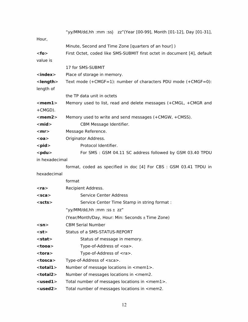
The block diagram of the project, shown in Figure2.1, displays these units and
their interfacing with the microcontroller.
`
Figure 2.1 BLOCK DIAGRAM OF THE PROJECT
2.1 DESIGN METHOD
Considering the variety and the complexity of the functions to be performed and
the fact that a rather complex controlling structure needs to coordinate the overall activity
of the system, a microcontroller-based system is ideally suited for this application. In
8051 BASEDAT 89S52
UART
ULN2003
Relay1 toControl D1
Relay2 toControl D2
Relay3 toControl D3
Relay4 toControl D4
MAX 232
GSM MODEM
SERIAL RS232
SIM
TTL
RS232
ALL THE RELAYS ARE ELECTROMAGNETIC RELAYS
D1, D2, D3, D4 ARE THE DEVICES OF ANY TYPE EITHER AC OR DC
THESE RELAYS MAY SWITHAC UP TO 7A, 300V, 50HZDC UP TO 10A, 28V
ULN 2003 IS NPN TYPE DARLINGTON TRANSISTOR ARRAY
17

addition to coordinating the functions of the system, the controller itself may be used to
simplify the implementation of some of the desired functions or tasks (like counting,
comparison of data, interrupts handling etc.). The use of a microcontroller has the
advantage that it has a CPU (a microprocessor) in addition to a fixed amount of
RAM,ROM,I/O ports & timer are all embedded together on one chip, thus decreasing the
size and cost of the system. Future design changes are quickly and easily implemented,
primarily by changing the program. Thus reducing the shop and material costs. Also,
software is more flexible than hardware.
The Top-Down policy approach has been followed in the design of this system.
This approach is basically a step-wise refinement. First, the general structure is created.
The problem is broken into smaller segments and each one is dealt with individually.
This process is repeated until the problem segment in hand is manageable.
The basic functions to be performed by this system could be distinctively divided in the
following manner:
• Check for message indication
• reading the SMS
• Verify number
• verify command
• Operate Device
• Send Feedback
The controller is continuously looking for inputs from the GSM modem (SMS). If the
input is a legal command, the routine that performs that desired function is called and the
function is performed.
2.2 PROJECT LAYOUT
The whole project comprises of five basic units. These units were built and tested
separately, and then combined to get the fully functional device. The five basic units are:
1. The GSM (Global System for Mobile Communication) Modem.
2. The Max 232 Serial Interface
3. The 8051 BASED AT 89S52 Microcontroller
4. The ULN 2003, and
18

5. The RELAYS.
2.3 SCHEMATIC REPRESTATION OF PROJECT WITH INTERFACING
19

2.4 WORKING
In this project we are using AT89s52 Microcontroller which belongs to the 8051
family (MCS51 Popular INTEL Architecture) .In this controller the pins 18 and 19 are
XTAL1 and XTAL2 respectively and they are connected to 11.0592 MHz crystal, to
generate clock pulses to the internal oscillator circuit.
If the Power is “ON” the 10micro farad capacitor is connected across the 9th pin (i.e. reset
pin) of micro controller discharges and produces a pulse on the reset pin due to that the
reset interrupt occurs which serve reset ISR i.e. from 0th location of the program memory.
From that the 10 micro farad capacitor blocked DC voltage (5v) goes to 40th (VCC) and
30th (ĒĀ) pins and 20th pin is grounded.
In this project we are disabling the external access pin due to the
use of internal program memory (8Konly).in our project the main interfacing are LCD,
serial communication, relay interfacing.
2.4.1 LCD
It is connected to port0 of 89s52 & 3 control signals RS, RD, WR& enabled to port
3.5,3.6 &3.7. Here we are using LCD to display the status of the devices like whether the
devices are in the ON or OFF state.
For serial communication we are using Max 232 line driver line IC to convert
TTL levels into RS232 and vice versa. The main function of this serial communication is
to communicate with the GSM modem inRS232 protocol using MAX 232 IC.
2.4.2 Relays:
To control that devices we are using Electromechanical switches (Relays) which are
connected to ULN2003 output pins. ULN2003 is used to control the relay ground pins i.e.
current sinking because the microcontroller is having not that much of the capacity to
control the Relay ground directly(current consumption is high) so we are using ULN2003
which is having seven NPN type Darlington pairs, so we can control seven relays and we
20

are using 12V DC operating relays. These Relays can switch 50Hz 250V so we can
directly switch the liner and household devices.
EXPLANATION OF INDIVIDUAL BLOCKS
2.5. ATMEL 89S52 Microcontroller
2.5.1. Features:-
The Following are the important features of 89s52 microcontroller.
• Compatible with MCS-51(r) Products
• 8K Bytes of In-System Programmable (ISP) Flash Memory
Endurance: 1000 Write/Erase Cycles
• 4.0V to 5.5V Operating Range
• Fully Static Operation: 0 Hz to 33 MHz
• Three-level Program Memory Lock
• 256 x 8-bit Internal RAM
• 32 Programmable I/O Lines
• Three 16-bit Timer/Counters
• Eight Interrupt Sources
• Full Duplex UART Serial Channel
• Low-power Idle and Power-down Modes
• Interrupt Recovery from Power-down Mode
2.5.2 Description
The AT89S52 is a low-power, high-performance CMOS 8-bit microcontroller with 8K
bytes of in-system programmable Flash memory. The device is manufactured using
Atmel's high-density nonvolatile memory technology and is compatible with the
industry-standard 80C51 instruction set and pinout. The on-chip Flash allows the
program memory to be reprogrammed in-system or by a conventional nonvolatile
memory programmer.
By combining a versatile 8-bit CPU with in-system programmable Flash on a monolithic
chip, the Atmel AT89S52 is a powerful microcontroller which provides a highly-flexible
21

and cost-effective solution to many embedded control applications. The AT89S52
provides the following standard features: 8K bytes of Flash, 256 bytes of RAM, 32 I/O
lines, two data pointers, three 16-bit timer/counters, a six-vector two-level interrupt
architecture, a full duplex serial port, on-chip oscillator, and clock circuitry. In addition,
the AT89S52 is designed with static logic for operation down to zero frequency and
supports two software selectable power saving modes.
The Idle Mode stops the CPU while allowing the RAM, timer/counters, serial port, and
interrupt system to continue functioning. The Power-down mode saves the RAM contents
but freezes the oscillator, disabling all other chip functions until the next interrupt
or hardware reset.
22

2.5.3 Diagram of AT89s52
Figure 2.3 The given below is the block diagram.
23

24

2.5.4 PIN CONFIGURATION
25

Figure 2.4 pin configuration of AT89S52 I.C
VCC
Supply voltage.
GND
Ground.
Port 0
Port 0 is an 8-bit open drain bidirectional I/O port. As an output port, each pin can sink
eight TTL inputs. When 1s are written to port 0 pins, the pins can be used as high
impedance inputs.
Port 0 can also be configured to be the multiplexed low order address/data bus during
accesses to external program and data memory. In this mode, P0 has internal pullups.
Port 0 also receives the code bytes during Flash programming and outputs the code bytes
during program verification. External pullups are required during program verification.
Port 1
Port 1 is an 8-bit bidirectional I/O port with internal pullups. The Port 1 output buffers
can sink/source four TTL inputs. When 1s are written to Port 1 pins, they are pulled high
26

by the internal pullups and can be used as inputs. As inputs, Port 1 pins that are externally
being pulled low will source current (IIL) because of the internal pullups.
In addition, P1.0 and P1.1 can be configured to be the timer/counter 2 external count
input (P1.0/T2) and the timer/counter 2 trigger input (P1.1/T2EX), respectively, as shown
in the following table.
Port 1 also receives the low-order address bytes during Flash programming and
verification.
Port Pin Alternate Functions
P1.0 T2 (external count input to Timer/Counter 2), clock-out
P1.1 T2EX (Timer/Counter 2 capture/reload trigger and direction control)
P1.5 MOSI (used for In-System Programming)
P1.6 MISO (used for In-System Programming)
P1.7 SCK (used for In-System Programming)
Port 2
Port 2 is an 8-bit bidirectional I/O port with internal pullups. The Port 2 output buffers
can sink/source four TTL inputs. When 1s are written to Port 2 pins, they are pulled high
by the internal pullups and can be used as inputs. As inputs, Port 2 pins that are externally
being pulled low will source current (IIL) because of the internal pullups.
Port 2 emits the high-order address byte during fetches from external program
memory and during accesses to external data memory that uses 16-bit addresses (MOVX
@DPTR). In this application, Port 2 uses strong internal pullups when emitting 1s.
During accesses to external data memory that use 8-bit addresses (MOVX @ RI), Port 2
emits the contents of the P2 Special Function Register.
27

Port 2 also receives the high-order address bits and some control signals during Flash
programming and verification.
Port 3
Port 3 is an 8-bit bidirectional I/O port with internal pullups. The Port 3 output buffers
can sink/source four TTL inputs. When 1s are written to Port 3 pins, they are pulled high
by the internal pullups and can be used as inputs. As inputs, Port 3 pins that are externally
being pulled low will source current (IIL) because of the pullups.
Port 3 also serves the functions of various special features of the AT89S52, as shown in
below.
Port 3 also receives some control signals for Flash programming and verification.
Port Pin Alternate Functions
P3.0 RXD (serial input port)
P3.1 TXD (serial output port)
P3.2 INT0 (external interrupt 0)
P3.3 INT1 (external interrupt 1)
P3.4 T0 (timer 0 external input)
P3.5 T1 (timer 1 external input)
P3.6 WR (external data memory write strobe)
P3.7 RD (external data memory read strobe)
RST
Reset input. A high on this pin for two machine cycles while the oscillator is running
resets the device
ALE/PROG
28

Address Latch Enable (ALE) is an output pulse for latching the low byte of the address
during accesses to external memory. This pin is also the program pulse input (PROG)
during Flash programming.
In normal operation, ALE is emitted at a constant rate of 1/6 the oscillator frequency and
may be used for external timing or clocking purposes. Note, however, that one ALE pulse
is skipped during each access to external data memory.
If desired, ALE operation can be disabled by setting bit 0 of SFR location 8EH. With the
bit set, ALE is active only during a MOVX or MOVC instruction. Otherwise, the pin is
weakly pulled high. Setting the ALE-disable bit has no effect if the microcontroller is in
external execution mode.
PSEN
This is an output pin. Program Store Enable (PSEN) is the read strobe to external
program memory. When the AT89S52 is executing code from external program memory,
PSEN is activated twice each machine cycle, except that two PSEN activations are
skipped during each access to external data memory.
EA/VPP
External Access Enable. EA must be strapped to GND in order to enable the device to
fetch code from external program memory locations starting at 0000H up to FFFFH.
Note, however, that if lock bit 1 is programmed, EA will be internally latched on reset
EA should be strapped to VCC for internal program executions. This pin also receives the
12-volt programming enable voltage (VPP) during Flash programming.
XTAL1 and XTAL2
29

The microcontroller has on-chip oscillators but requires an external clock to run it most
often a quartz crystal oscillator is connected to inputs XTAL1(PIN19) & XTAL2
(PIN18). The quartz crystal oscillator connected to XTAL1 and XTAL2 also needs two
capacitors of 30pF value. One side of each capacitor is connected to the ground.
It must be noted that there are various speeds of the AT 89s52 family. Speed refers to the
maximum oscillator frequency connected to XTAL. For example, a 12-MHz chip must be
connected to a crystal with 12MHz frequency or less. Likewise, a 20-MHz requires a
crystal frequency of no more than 20 MHz. When the microcontroller is connected to a
crystal oscillator and is powered up, we can observe the frequency on the XTAL2 pin
using the oscilloscope.
If you decide to use a frequency source other than a crystal oscillator, such as a
TTL oscillator, it will be connected to XTAL1; XTAL2 is left unconnected.
Input to the inverting oscillator amplifier and input to the internal clock operating circuit.
Out from the inverting oscillator amplifier.
Oscillator Characteristics
30

XTAL1 and XTAL2 are the input and output, respectively, of an inverting amplifier that
can be configured for use as an on-chip oscillator, as shown in Figure 2.5 Either a quartz
crystal or ceramic resonator may be used. To drive the device from an external clock
source, XTAL2 should be left unconnected while XTAL1 is driven, as shown in Figure
2.6 There are no requirements on the duty cycle of the external clock signal, since the
input to the internal clocking circuitry is through a divide-by-two flip-flop, but minimum
and maximum voltage high and low time specifications must be observed.
Figure 2.5 oscillator connections
Note: C1, C2 = 30 pF ± 10 pF for Crystals
= 40 pF ± 10 pF for Ceramic Resonators
31

Figure 2.6 External Clock Drive Configuration
Special Function Registers
A map of the on-chip memory area called the Special Function Register (SFR) space is
shown in Table 3.1.
Note that not all of the addresses are occupied, and unoccupied addresses may not be
implemented on the chip. Read accesses to these addresses will in general return random
data, and write accesses will have an indeterminate effect.
32

User software should not write 1s to these unlisted locations, since they may be used in
future products to invoke new features. In that case, the reset or inactive values of the
new bits will always be 0.
Timer 2 Registers: Control and status bits are contained in registers T2CON (shown in
Table 2.2) and T2MOD (shown in Table 2.3) for Timer 2. The register pair (RCAP2H,
RCAP2L) are the Capture/Reload registers for Timer 2 in 16-bit capture mode or 16-bit
auto-reload mode.
Interrupt Registers: The individual interrupt enable bits are in the IE register. Two
priorities can be set for each of the six interrupt sources in the IP register.
T2CON - Timer/Counter 2 Control Register
T2CON Address = 0C8H Reset Value = 0000 0000B
TF2 EXF2 RCLK TCLK EXEN2 TR2 C/T2 CP/RL27 6 5 4 3 2 1 0
Table 2.1. Bit Addressable Bit
Table 2.2. AUXR: Auxiliary Register
Symbol FunctionTF2 Timer 2 overflow flag set by a Timer 2 overflow and must be cleared by
software.
TF2 will not be set when either RCLK = 1 or TCLK = 1.EXF2 Timer 2 external flag set when either a capture or reload is caused by a
negative transition
on T2EX and EXEN2 = 1. When Timer 2 interrupt is enabled, EXF2 = 1 will
33

cause the CPU to vector to the Timer 2 interrupt routine. EXF2 must be cleared
by software.
EXF2 does not cause an interrupt in up/down counter mode (DCEN = 1).RCLK Receive clock enable. When set, causes the serial port to use Timer 2 overflow
pulses
for its receive clock in serial port Modes 1 and 3. RCLK = 0 causes Timer 1
overflow
to be used for the receive clock.TCLK Transmit clock enable. When set, causes the serial port to use Timer 2
overflow pulses for its transmit clock in serial port
Modes 1 and 3. TCLK = 0 causes Timer 1 overflows to be used for the transmit
clock.EXEN2 Timer 2 external enables. When set, allows a capture or reload to occur as a
result of a negative
transition on T2EX if Timer 2 is not being used to clock the serial port.
EXEN2 = 0 causes Timer 2 to ignore events at T2EX.TR2 Start/Stop control for Timer 2. TR2 = 1 starts the timer.C/T2 Timer or counter select for Timer 2. C/T2 = 0 for timer function. C/T2 = 1
for external event counter (falling edge triggered).CP/RL2 Capture/Reload select. CP/RL2 = 1 causes captures to occur on negative
transitions at T2EX
if EXEN2 = 1. CP/RL2 = 0 causes automatic reloads to occur when Timer 2
overflows or
negative transitions occur at T2EX when EXEN2 = 1. When either RCLK or
TCLK = 1,
this bit is ignored and the timer is forced to auto-reload on Timer 2 overflow.
AUXR Address = 8EH Reset Value = XXX00XX0B
- - - WDIDLE DISRTO - - DISALE7 6 5 4 3 2 1 0Table 2.3. Non-Bit Addressable Bit
34

- Reserved for future expansion
DISALE Disable/Enable ALE
DISALE Operating Mode
0 ALE is emitted at a constant rate of 1/6 the oscillator frequency
1 ALE is active only during a MOVX or MOVC instruction
DISRTO Disable/Enable Reset out
DISRTO
0 Reset pin is driven High after WDT times out
1 Reset pin is input only
WDIDLE Disable/Enable WDT in IDLE mode
WDIDLE
0 WDT continues to count in IDLE mode
WDT halts counting in IDLE mode
Dual Data Pointer Registers:
To facilitate accessing both internal and external data memory , two banks of 16-bit Data
Pointer Registers are provided: DP0 at SFR address locations 82H-83H and DP1 at 84H-
85H. Bit DPS = 0 in SFR AUXR1 selects DP0 and DPS = 1 selects DP1. The user should
always initialize the DPS bit to the appropriate value before accessing the respective Data
Pointer Register.
Power Off Flag:
The Power Off Flag (POF) is located at bit 4 (PCON.4) in the PCON SFR. POF is set to
"1" during power up. It can be set and rest under software control and is not affected by
reset.
35

AUXR1: Auxiliary Register 1
AUXR1 Address = A2H Reset Value = XXXXXXX0B
Not Bit Addressable
- - - - - - - DPS7 6 5 4 3 2 1 0
Table2.4 Auxiliary Register 1
- Reserved for future expansion
DPS Data Pointer Register Select
DPS
0 Selects DPTR Registers DP0L, DP0H
1 Selects DPTR Registers DP1L, DP1H
2.5.5 Memory Organization
MCS-51 devices have a separate address space for Program and Data Memory. Up to
64K bytes each of external Program and Data Memory can be addressed.
2.5.5.1 Program Memory
If the EA pin is connected to GND, all program fetches are directed to external memory.
On the AT89S52, if EA is connected to VCC, program fetches to addresses 0000H
through 1FFFH are directed to internal memory and fetches to addresses 2000H through
FFFFH are to external memory.
2.5.5.2 Data Memory
The AT89S52 implements 256 bytes of on-chip RAM. The upper 128 bytes occupy a
parallel address space to the Special Function Registers. This means that the upper 128
bytes have the same addresses as the SFR space but are physically separate from SFR
space. When an instruction accesses an internal location above address 7FH, the address
mode used in the instruction specifies whether the CPU accesses the upper 128 bytes of
RAM or the SFR space. Instructions which use direct addressing access of the SFR space.
36

For example, the following direct addressing instruction accesses the SFR at location
0A0H (which is P2).
MOV 0A0H, #data
Instructions that use indirect addressing access the upper 128 bytes of RAM. For
example, the following indirect addressing instruction, where R0 contains 0A0H,
accesses the data byte at address 0A0H, rather than P2 (whose address is 0A0H).
MOV @R0, #data
Note that stack operations are examples of indirect addressing, so the upper 128 bytes of
data RAM are available as stack space.
2.5.6 Timers
The 8051 based AT89s52 microcontroller has three Timers/Counters they can be used
either as Timers to generate time delay or as
2.5.6.1 Timer 0 and 1
Timer 0 and Timer 1 in the AT89S52 operate the same way as Timer 0 and Timer 1 in
the AT89C51 and AT89C52
2.5.6.2 Timer 2
Timer 2 is a 16-bit Timer/Counter that can operate as either a timer or an event counter.
The type of operation is selected by bit C/T2 in the SFR T2CON (shown in Table 3.1).
Timer 2 has three operating modes: capture, auto-reload modes are selected by bits in
T2CON, as shown in Table 3.5. Timer 2 consists of two 8-bit registers, TH2 and TL2. In
the Timer function, the TL2 register is incremented every machine cycle. Since a
machine cycle consists of 12 oscillator periods, the count rate is 1/12 of the oscillator
frequency.
37

Table 2.5. Timer 2 Operating Modes
RCLK +TCLK CP/RL2 TR2 MODE0 0 1 16-bit Auto-reload0 1 1 16-bit Capture1 X 1 Baud Rate GeneratorX X 0 (Off)
In the Counter function, the register is incremented in response to a 1-to-0 transition at its
corresponding external input pin, T2. In this function, the external input is sampled
during S5P2 of every machine cycle. When the samples show a high in one cycle and a
low in the next cycle, the count is incremented. The new count value appears in the
register during S3P1 of the cycle following the one in which the transition was detected.
Since two machine cycles (24 oscillator periods) are required to recognize a 1-to-0
transition, the maximum count rate is 1/24 of the oscillator frequency. To ensure that a
given level is sampled at least once before it changes, the level should be held for at least
one full machine cycle.
Capture Mode
In the capture mode, two options are selected by bit EXEN2 in T2CON. If EXEN2 = 0,
Timer 2 is a 16-bit timer or counter which upon overflow sets bit TF2 in T2CON. This bit
can then be used to generate an interrupt. If EXEN2 = 1, Timer 2 performs the same
operation, but a 1- to-0 transition at external input T2EX also causes the current value in
TH2 and TL2 to be captured into RCAP2H and RCAP2L, respectively. In addition, the
transition at T2EX causes bit EXF2 in T2CON to be set. The EXF2 bit, like TF2, can
generate an interrupt.
Auto-reload (Up or Down Counter)
Timer 2 can be programmed to count up or down when configured in its 16-bit auto-
reload mode. This feature is invoked by the DCEN (Down Counter Enable) bit located in
the SFR T2MOD. Upon reset, the DCEN bit is set to 0 so that timer 2 will default to
count up. When DCEN is set, Timer 2 can count up or down, depending on the value of
the T2EX pin.
38

Timer 2 automatically counts up when DCEN=0. In this mode, two options are selected
by bit EXEN2 in T2CON. If EXEN2 = 0, Timer 2 counts up to 0FFFFH and then sets the
TF2 bit upon overflow. The overflow also causes the timer registers to be reloaded with
the 16-bit value in RCAP2H and RCAP2L. The values in Timer in Capture
ModeRCAP2H and RCAP2L are preset by software. If EXEN2 = 1, a 16-bit reload can
be triggered either by an overflow or by a 1-to-0 transition at external input T2EX. This
transition also sets the EXF2 bit. Both the TF2 and EXF2 bits can generate an interrupt if
enabled. Setting the DCEN bit enables Timer 2 to count up or down. In this mode, the
T2EX pin controls the direction of the count. A logic 1 at T2EX makes Timer 2 count up.
The timer will overflow at 0FFFFH and set the TF2 bit. This overflow also causes the 16-
bit value in RCAP2H and RCAP2L to be reloaded into the timer registers, TH2 and TL2,
respectively.
A logic 0 at T2EX makes Timer 2 count down. The timer underflows when TH2 and TL2
equal the values stored in RCAP2H and RCAP2L. The underflow sets the TF2 bit and
causes 0FFFFH to be reloaded into the timer registers. The EXF2 bit toggles whenever
Timer 2 overflows or underflows and can be used as a 17th bit of resolution. In this
operating mode, EXF2 does not flag an interrupt.
Table2.6 T2MOD - Timer 2 Mode Control Register
T2MOD Address = 0C9H Reset Value = XXXX XX00B
Not Bit Addressable
- - - - - - T2OE DCEN7 6 5 4 3 2 1 0
Symbol Function- Not implemented, reserved for futureT2OE Timer 2 Output Enable bitDCEN When set, this bit allows Timer 2 to be configured as an up/down counter
39

Baud Rate Generator
Timer 2 is selected as the baud rate generator by setting TCLK and/or RCLK in T2CON.
Note that the baud rates for transmit and receive can be different if Timer 2 is used for the
receiver or transmitter and Timer 1 is used for the other function. Setting RCLK and/or
TCLK puts Timer 2 into its baud rate generator mode.
The baud rate generator mode is similar to the auto-reload mode, in that a rollover in TH2
causes the Timer 2 registers to be reloaded with the 16-bit value in registers RCAP2H
and RCAP2L, which are preset by software. The baud rates in Modes 1 and 3 are
determined by Timer 2's overflow rate according to the following equation.
Modes 1 and 3 Baud Rates =Timer 2 Overflow Rate /16
The Timer can be configured for either timer or counter operation. In most applications, it
is configured for timer operation (CP/T2 = 0). The timer operation is different for Timer
2 when it is used as a baud rate generator. Normally, as a timer, it increments every
machine cycle (at 1/12 the oscillator frequency). As a baud rate generator, however, it
increments every state time (at 1/2 the oscillator frequency).
Note that a rollover in TH2 does not set TF2 and will not generate an interrupt. Note too,
that if EXEN2 is set, a 1-to-0 transition in T2EX will set EXF2 but will not cause a
reload from (RCAP2H, RCAP2L) to (TH2, TL2). Thus, when Timer 2 is in use as a baud
rate generator, T2EX can be used asan extra external interrupt. Note that when Timer 2 is
running (TR2 = 1) as a timer in the baud rate generator mode, TH2 or TL2 should not be
read from or written to.
Under these conditions, the Timer is incremented every state time, and the results of a
read or write may not be accurate. The RCAP2 registers may be read but should not be
written to, because a write might overlap a reload and cause write and/or reload errors.
The timer should be turned off (clear TR2) before accessing the Timer 2 or RCAP2
registers.
40

Programmable Clock Out
A 50% duty cycle clock can be programmed to come out on P1.0. This pin, besides being
a regular I/O pin, has two alternate functions. It can be programmed to input the external
clock for Timer/Counter 2 or to output a 50% duty cycle clock ranging from 61 Hz to 4
MHz at a 16 MHz operating frequency. To configure the Timer/Counter 2 as a clock
generator, bit C/T2 (T2CON.1) must be cleared and bit T2OE (T2MOD.1) must be set.
Bit TR2 (T2CON.2) starts and stops the timer. The clock-out frequency depends on the
oscillator frequency and the reload value of Timer 2 capture registers (RCAP2H,
RCAP2L), as shown in the following equation.
Clock-Out Frequency = Oscillator Frequency /(4 x [65536-(RCAP2H,RCAP2L)] )
In the clock-out mode, Timer 2 roll-overs will not generate an interrupt. This behavior is
similar to when Timer 2 is used as a baud-rate generator. It is possible to use Timer 2 as a
baud-rate generator and a clock generator simultaneously. Note, however, that the baud-
rate and clock-out frequencies cannot be determined independently from one another
since they both use RCAP2H and RCAP2L.
2.5.7 Interrupts
The AT89S52 has a total of six interrupt vectors: two external interrupts (INT0 and
INT1), three timer interrupts (Timers 0, 1, and 2), and the serial port interrupt.Each of
these interrupt sources can be individually enabled or disabled by setting or clearing a bit
in Special Function Register IE. IE also contains a global disable bit, EA, which disables
all interrupts at once.
Note that Table 2.7 shows that bit position IE.6 is unimplemented. In the AT89S52, bit
position IE.5 is also unimplemented. User software should not write 1s to these bit
positions, since they may be used in future AT89 products. Timer 2 interrupt is generated
by the logical OR of bits TF2 and EXF2 in register T2CON. Neither of these flags is
cleared by hardware when the service routine is vectored to. In fact, the service routine
41

may have to determine whether it was TF2 or EXF2 that generated the interrupt, and that
bit will have to be cleared in software.
The Timer 0 and Timer 1 flags, TF0 and TF1, are set at S5P2 of the cycle in which the
timers overflow. The values are then polled by the circuitry in the next cycle. However,
the Timer 2 flag, TF2, is set at S2P2 and is polled in the same cycle in which the timer
overflows.
Table 2.7. Interrupt Enable (IE) Register
(MSB) (LS B)
EA - ET2 ES ET1 EX1 ET0 EX0
Enable Bit = 1 enables the interrupt.
Enable Bit = 0 disables the interrupt.
User software should never write 1s to unimplemented bits, because they may be used in
future AT89 products.
Table 2.8 Interrupts Enables Description
Symbol Position FunctionEA IE.7 Disables all interrupts. If EA = 0, no interrupt is acknowledged If
EA= 1, each interrupt source is individually enabled or disabled By
setting or clearing its enable bit.- IE.6 Reserved.ET2 IE.5 Timer 2 interrupt enable bit.ES IE.4 Serial Port interrupt enable bit.ET1 IE.3 Timer 1 interrupt enable bit.EX1 IE.2 External interrupt 1 enable bit.ET0 IE.1 Timer 0 interrupt enable bit.EX0 IE.0 External interrupt 0 enable bit.
42

Figure 2.7 Interrupt Sources
Idle Mode
In idle mode, the CPU puts itself to sleep while all the on chip peripherals remain active.
The mode is invoked by software. The content of the on-chip RAM and all the special
43

functions registers remain unchanged during this mode. The idle mode can be terminated
by any enabled interrupt or by a hardware reset.
Note that when idle mode is terminated by a hardware reset, the device normally resumes
program execution from where it left off, up to two machine cycles before the internal
reset algorithm takes control. On-chip hardware inhibits access to internal RAM in this
event, but access to the port pins is not inhibited. To eliminate the possibility of an
unexpected write to a port pin when idle mode is terminated by a reset, the instruction
following the one that invokes idle mode should not write to a port pin or to external
memory.
Power-down Mode
In the Power-down mode, the oscillator is stopped, and the instruction that invokes
Power-down is the last instruction executed. The on-chip RAM and Special Function
Registers retain their values until the Power-down mode is terminated. Exit from Power-
down mode can be initiated either by a hardware reset or by an enabled external interrupt.
Reset redefines the SFRs but does not change the on-chip RAM.
The reset should not be activated before VCC is restored to its normal operating level and
must be held active long enough to allow the oscillator to restart and stabilize.
Table 2.9. Status of External Pins During Idle and Power-Down Modes
Mode Program
Memory
ALE PSEN PORT0 PORT1 PORT2 PORT3
Idle Internal 1 1 Data Data Data DataIdle External 1 1 Float Data Address DataPower-
down
Internal 0 0 Data Data Data Data
Power-
down
External 0 0 Float Data Data Data
44

2.6 SERIAL INTERFACE Max 232:-
2.6.1 INTRODUCTION:
The Serial Port is harder to interface than the Parallel Port. In most cases, any device you
connect to the serial port will need the serial transmission converted back to parallel so
that it can be used. This can be done using a UART. On the software side of things, there
are many more registers that you have to attend to than on a Standard Parallel Port. (SPP)
1. Serial Cables can be longer than Parallel cables. The serial port transmits a '1' as -3 to
-25 volts and a '0' as +3 to +25 volts where as a parallel port transmits a '0' as 0v and a
'1' as 5v. Therefore the serial port can have a maximum swing of 50V compared to the
parallel port which has a maximum swing of 5 Volts. Therefore cable loss is not going
to be as much of a problem for serial cables, as they are for parallel. 2. You don't need as many wires then parallel transmission. If your device needs to be
mounted a far distance away from the computer then 3 core cable (Null Modem
Configuration) is going to be a lot cheaper that running 19 or 25 core cable. However
you must take into account the cost of the interfacing at each end.
3. Microcontroller's have also proven to be quite popular recently. Many of these have in
built SCI (Serial Communications Interfaces) which can be used to talk to the outside
world. Serial Communication reduces the pin count of these MPU's. Only two pins are
commonly used, Transmit Data (TXD) and Receive Data (RXD) compared with at least
8 pins if you use a 8 bit Parallel method (You may also require a Strobe).
45

2.6.2 Hardware Properties:
Figure2.8: Typical operating circuit
Devices which use serial cables for their communication are split into two categories.
These are DCE (Data Communications Equipment) and DTE (Data Terminal
Equipment.) Data Communications Equipments are devices such as your modem, TA
adapter, plotter etc while Data Terminal Equipment is your Computer or Terminal.
The electrical specifications of the serial port are contained in the EIA (Electronics
Industry Association) RS232C standard. It states many parameters such as –
46

1. A "Space" (logic 0) will be between +3 and +25 Volts. 2. A "Mark" (Logic 1) will be between -3 and -25 Volts. 3. The region between +3 and -3 volts is undefined. 4. An open circuit voltage should never exceed 25 volts.
(In Reference to GND) 5. A short circuit current should not exceed 500mA. The
driver should be able to handle this without damage.
(Take note of this one!) Electrical Parameters of MAX 232 I.C
Above is no where near a complete list of the EIA standard. Line Capacitance, Maximum
Baud Rates etc are also included. For more information please consult the EIA RS232-C
standard. It is interesting to note however, that the RS232C standard specifies a
maximum baud rate of 20,000 BPS!, which is rather slow by today's standards. A new
standard, RS-232D has been recently released.
2.6.3 PIN CONFIGURATION
Fig 2.9 pin configuration of Max232
47

2.6.4 PIN DESCRIPTION
Bit Name Bit Address Explanation of Function
7 SM0 9Fh Serial port mode bit 0
6 SM1 9Eh Serial port mode bit 1.
5 SM2 9Dh Multiprocessor Communications Enable (explained later)
4 REN 9ChReceiver Enable. This bit must be set in order to receive
characters.
3 TB8 9Bh Transmit bit 8. The 9th bit to transmit in mode 2 and 3.
2 RB8 9Ah Receive bit 8. The 9th bit received in mode 2 and 3.
1 TI 99hTransmit Flag. Set when a byte has been completely
transmitted.
0 RI 98h Receive Flag. Set when a byte has been completely received.
Table2.10 pin description of Max232
Additionally, it is necessary to define the function of SM0 and SM1 by an additional
table: Table 2.11 Functions of SM0 and SM1
SM0 SM1 Serial Mode Explanation Baud Rate
0 0 0 8-bit Shift Register Oscillator / 12
0 1 1 8-bit UART Set by Timer 1 (*)
1 0 2 9-bit UART Oscillator / 32 (*)
1 1 3 9-bit UART Set by Timer 1 (*)
(*) Note: The baud rate indicated in this table is doubled if PCON.7 (SMOD) is set.
The SCON SFR allows us to configure the Serial Port. Thus, we’ll go through each bit
and review it’s function.
The first four bits (bits 4 through 7) are configuration bits.
Bits SM0 and SM1 let us set the serial mode to a value between 0 and 3, inclusive. The
four modes are defined in the chart immediately above. As you can see, selecting the
Serial Mode selects the mode of operation (8-bit/9-bit, UART or Shift Register) and also
determines how the baud rate will be calculated. In modes 0 and 2 the baud rate is fixed
based on the oscillator’s frequency. In modes 1 and 3 the baud rate is variable based on
48

how often Timer 1 overflows. We’ll talk more about the various Serial Modes in a
moment.
The next bit, SM2, is a flag for "Multiprocessor communication." Generally, whenever a
byte has been received the 8051 will set the "RI" (Receive Interrupt) flag. This lets the
program know that a byte has been received and that it needs to be processed. However,
when SM2 is set the "RI" flag will only be triggered if the 9th bit received was a "1".
That is to say, if SM2 is set and a byte is received whose 9th bit is clear, the RI flag will
never be set. This can be useful in certain advanced serial applications. For now it is safe
to say that you will almost always want to clear this bit so that the flag is set upon
reception of any character.
The next bit, REN, is "Receiver Enable." This bit is very straightforward: If you want to
receive data via the serial port, set this bit. You will almost always want to set this bit.
The last four bits (bits 0 through 3) are operational bits. They are used when actually
sending and receiving data--they are not used to configure the serial port.
The TB8 bit is used in modes 2 and 3. In modes 2 and 3, a total of nine data bits are
transmitted. The first 8 data bits are the 8 bits of the main value, and the ninth bit is taken
from TB8. If TB8 is set and a value is written to the serial port, the data’s bits will be
written to the serial line followed by a "set" ninth bit. If TB8 is clear the ninth bit will be
"clear."
The RB8 also operates in modes 2 and 3 and functions essentially the same way as TB8,
but on the reception side. When a byte is received in modes 2 or 3, a total of nine bits are
received. In this case, the first eight bits received are the data of the serial byte received
and the value of the ninth bit received will be placed in RB8.
TI means "Transmit Interrupt." When a program writes a value to the serial port, a certain
amount of time will pass before the individual bits of the byte are "clocked out" the serial
port. If the program were to write another byte to the serial port before the first byte was
completely output, the data being sent would be garbled. Thus, the 8051 lets the program
know that it has "clocked out" the last byte by setting the TI bit. When the TI bit is set,
the program may assume that the serial port is "free" and ready to send the next byte.
Finally, the RI bit means "Receive Interrupt." It functions similarly to the "TI" bit, but it
indicates that a byte has been received. That is to say, whenever the 8051 has received a
49

complete byte it will trigger the RI bit to let the program know that it needs to read the
value quickly, before another byte is read.
Setting the Serial Port Baud Rate
Once the Serial Port Mode has been configured, as explained above, the program must
configure the serial port’s baud rate. This only applies to Serial Port modes 1 and 3. The
Baud Rate is determined based on the oscillator’s frequency when in mode 0 and 2. In
mode 0, the baud rate is always the oscillator frequency divided by 12. This means if
you’re crystal is 11.059 Mhz, mode 0 baud rate will always be 921,583 baud. In mode 2
the baud rate is always the oscillator frequency divided by 64, so a 11.059Mhz crystal
speed will yield a baud rate of 172,797.
In modes 1 and 3, the baud rate is determined by how frequently timer 1 overflows. The
more frequently timer 1 overflows, the higher the baud rate. There are many ways one
can cause timer 1 to overflow at a rate that determines a baud rate, but the most common
method is to put timer 1 in 8-bit auto-reload mode (timer mode 2) and set a reload value
(TH1) that causes Timer 1 to overflow at a frequency appropriate to generate a baud rate.
To determine the value that must be placed in TH1 to generate a given baud rate, we may
use the following equation (assuming PCON.7 is clear).
TH1 = 256 - ((Crystal / 384) / Baud)
If PCON.7 is set then the baud rate is effectively doubled, thus the equation becomes:
TH1 = 256 - ((Crystal / 192) / Baud)
For example, if we have an 11.059Mhz crystal and we want to configure the serial port to
19,200 baud we try plugging it in the first equation:
TH1=256-((Crystal/384)/Baud)
TH1=256-((11059000/384)/19200)
TH1=256-((28,799)/19200)
TH1 = 256 - 1.5 = 254.5
As you can see, to obtain 19,200 baud on a 11.059Mhz crystal we’d have to set TH1 to
254.5. If we set it to 254 we will have achieved 14,400 baud and if we set it to 255 we
will have achieved 28,800 baud. Thus we’re stuck...
50

But not quite... to achieve 19,200 baud we simply need to set PCON.7 (SMOD). When
we do this we double the baud rate and utilize the second equation mentioned above.
Thus we have:
TH1=256-((Crystal/192)/Baud)
TH1=256-((11059000/192)/19200)
TH1=256-((57699)/19200)
TH1 = 256 - 3 = 253
Here we are able to calculate a nice, even TH1 value. Therefore, to obtain 19,200 baud
with an 11.059MHz crystal we must:
1.Configure Serial Port mode 1 or 3.
2.Configure Timer 1 to timer mode 2 (8-bit auto-reload).
3.Set TH1 to 253 to reflect the correct frequency for 19,200 baud.
4. Set PCON.7 (SMOD) to double the baud rate.
2.6.5 Writing to the Serial Port
Once the Serial Port has been properly configured as explained above, the serial port is
ready to be used to send data and receive data. If you thought that configuring the serial
port was simple, using the serial port will be a breeze.
To write a byte to the serial port one must simply write the value to the SBUF (99h) SFR.
For example, if you wanted to send the letter "A" to the serial port, it could be
accomplished as easily as:
MOV SBUF,#’A’
Upon execution of the above instruction the 8051 will begin transmitting the character
via the serial port. Obviously transmission is not instantaneous--it takes a measurable
amount of time to transmit. And since the 8051 does not have a serial output buffer we
need to be sure that a character is completely transmitted before we try to transmit the
next character.
The 8051 lets us know when it is done transmitting a character by setting the TI bit in
SCON. When this bit is set we know that the last character has been transmitted and that
we may send the next character, if any. Consider the following code segment:
51

CLR TI ;Be sure the bit is initially clear
MOV SBUF,#’A’ ;Send the letter ‘A’ to the serial port
JNB TI,$ ;Pause until the TI bit is set.
The above three instructions will successfully transmit a character and wait for the TI bit
to be set before continuing. The last instruction says "Jump if the TI bit is not set to $"--$,
in most assemblers, means "the same address of the current instruction." Thus the 8051
will pause on the JNB instruction until the TI bit is set by the 8051 upon successful
transmission of the character.
2.6.6 Reading the Serial Port
Reading data received by the serial port is equally easy. To read a byte from the serial
port one just needs to read the value stored in the SBUF (99h) SFR after the 8051 has
automatically set the RI flag in SCON.
For example, if your program wants to wait for a character to be received and
subsequently read it into the Accumulator, the following code segment may be used:
JNB RI,$ ;Wait for the 8051 to set the RI flag
MOV A,SBUF ;Read the character from the serial port
The first line of the above code segment waits for the 8051 to set the RI flag; again, the
8051 sets the RI flag automatically when it receives a character via the serial port. So as
long as the bit is not set the program repeats the "JNB" instruction continuously.
Once the RI bit is set upon character reception the above condition automatically fails
and program flow falls through to the "MOV" instruction which reads the value
2.7 Liquid Crystal Display Unit (LCD):-
2.7.1 Introduction: -
52

Liquid Crystal Displays are created by sandwiching a thin (10-12 micro mm) layer of a
liquid crystal fluid between two glass plates. A transparent, electrically conductive film
or back plane is put up on the rear glass sheet. The transparent sections of the conductive
film in the shape of the desired characters are coated on the front glass plate. When a
voltage is applied between a segment and the back plane, an electric field is created in the
region under the segment. This electric field changes the transmission of light through the
region under the segment film.
2.7.2 Liquid Crystal Display Description: -
In this project, JHD 162A Liquid Crystal Display (16x2), which is shown in Figure 3.9, is
interfaced with the CPU.
Figure 2.10 JHD 162A Liquid Crystal Display
The features of JHD 162A LCD is as follows: -
• 16 Characters x 2 Lines
• 5x7DotswithCursor
• Built-in controller
• +5v Power Supply
• 1/16 Duty Circle.
The pin description of the JHD 162A LCD without backlight is as shown in Table 2.13. If
the LCD is having Backlight, then it will have two more pins with pin numbers 15 & 16
connected to VCC and GND respectively.
53

Pin
numberSymbol Level I/O Function
1 Vss - - Power supply (GND)
2 Vcc - - Power supply (+5V)
3 Vee - - Contrast adjust
4 RS 0/1 I0= Instruction input
1 = Data input
5 R/W 0/1 I0 = Write to LCD module
1 = Read from LCD module
6 E 1, 1->0 I Enable signal
7 DB0 0/1 I/O Data bus line 0 (LSB)
8 DB1 0/1 I/O Data bus line 1
9 DB2 0/1 I/O Data bus line 2
10 DB3 0/1 I/O Data bus line 3
11 DB4 0/1 I/O Data bus line 4
12 DB5 0/1 I/O Data bus line 5
13 DB6 0/1 I/O Data bus line 6
14 DB7 0/1 I/O Data bus line 7 (MSB)
Table 2.12. Pin assignment for <= 80 character displays
An LCD allows an application to output a very specific message (or prompt) to the user,
making the application much more user friendly and impressive. LCD's are invaluable for
displaying status messages and information during application debug. ASCII-input LCDs
even though they have these advantages, they have a reputation of being difficult to hook
up and get to work. Most alphanumeric LCD's use a common controller chip and a
common connector interface. Both of these actions have resulted in alphanumeric LCDs
that range in size from 8 characters to 80 (arranged as 40 b 2 or 20 b 4) and are
interchangeable, without requiring hardware or software changes.
The ASCII code to be displayed is 8 bits long and is sent to the LCD either 4 or 8 bits at
time. If the 4-bit mode is used, two nibbles of data (sent high 4 bits then low 4 bits with
an E clock pulse with each nibble) are sent to make up a full 8-bit transfer. The "E" clock
is used to initiate the data transfer within the LCD. In the LCD there is a cursor,
54

This specifies where the next data character is to be written. This cursor can be moved or
be made invisible to blink. The blinking function is very rarely used because it is pretty
obnoxious.
Sending parallel data either as 4 or 8 bits are the two primary modes of operation.
While there are secondary considerations and modes deciding how to send the data to the
LCD is more critical decision to be made for an LCD interface application. 4-bit mode is
best used when the speed required in an application and at least 10 I/O pins are available.
4-bit mode requires minimum 6 bits. To wire a Microcontroller to an LCD 4-bit mode,
just the top 4-bits (DB4-7) are written as shown in the Figure 2.11 below:
Figure 2.11 Data Transfer using a 4-Bit Interface
Using a shift register so that a minimum of three I/O pins is required can further reduce
this. 8-bit mode could be used with a shift register, but a ninth bit (which will be used as
R/S) will be required.
The display contains two internal byte-wide registers, one for command (RS=0) and the
second for the characters to be displayed (RS=1). The R/S bit is used to select whether
data or an instruction is being transferred between the Microcontroller and the LCD. If
the bit is set, the byte at the current LCD cursor position can be read or written.When the
55

bit is reset, either an instruction is being sent to the LCD or the execution status of the
last instruction is read back (whether it has completed or not).
The display contains two internal byte-wide registers, one for command (RS=0) and the
second for characters to be displayed (RS=1). It also contains a user programmed RAM
area (the character RAM) that can be programmed to generate a desired character that can
be formed using a dot matrix.
To distinguish between these two data areas, the hex command byte 80 will be used to
signify that the display RAM address 00h is chosen.
Port 1 is used to furnish the commands or data byte and ports 3.2 to 3.4 furnish register
select and read/write levels. The display takes varying amounts of time to accomplish the
functions. LCD bit 7 is monitored for a long high (bus) to ensure the display is not over
written. A slightly more complicated LCD display (4 lines* 40 characters) is currently
being used in medical diagnostic systems to run a very familiar program.
2.7.3 Getting The LCD To Display Text: -
After successfully initializing the LCD and turning the display ON, one can begin to
display messages on the LCD by sending the correct instructions to it. Getting the LCD to
display text is a two-step process. First, the LCD's cursor must be moved to the LCD
address where the character is to be displayed. This is done with the "DDRAM Address
Set" command. Second, the actual character must be written to the cursor in order to store
it in the DDRAM at the cursor's location. This is performed with the "CGRAM/DDRAM
Data Write" command.
2.7.4 LCD Busy Flag Polling: -
The LCD will not accept new commands while it is busy with some internal operation.
This condition must be tested before sending a new command to the LCD. The "Busy
Flag/Address Read" instruction should be used for this purpose. The BF bit in this
56

instruction is the busy flag. When this bit is 1, LCD controller is busy. When BF is 0,
LCD is ready for the next command. In addition to busy flag polling, this instruction is
used to determine where the address of the LCD cursor is. Examples for Busy Flag
testing using both 4-bit and 8-bit interfaces are shown in figures 2.12 and 2.13
respectively.
Figure 2.12 Example of busy flag testing using a 4-bit interface.
Figure 2.13 Example of busy flag testing using an 8-bit interface.
Defining LCD Custom Characters: -
57

One of the nice features of the LCD is that it allows for the creation and use of up to eight
unique, user-defined characters. Character Generator RAM (CGRAM) has been added to
the LCD for this purpose. Before a custom character can be used it must be created. Each
character that can be displayed by the LCD is composed of a 5 x 8 grid of pixels or dots.
Each of these dots can be turned either ON or OFF when a character is being displayed.
Therefore, in order for the LCD controller to display a character, it must have a definition
of which of the character dots need to be turned ON.
2.7.5 Interfacing of LCD with 89s52 Microcontroller: -
In this project, the JHD 162A LCD is interfaced with the 89s52 Microcontroller. Port1
pins of 89s52 are used to read and write the data from LCD by interfacing P0.0 - P0.7
lines to D0-D7 lines of LCD. Similarly Port3 pins (P3.2-P3.4) are connected to control
pins of LCD i.e. E, R/W and RS pins respectively.
2.8 LIGHT EMITTING DIODE
2.8.1 Introduction to Light Emitting Diodes: -
A semiconductor P-N junction diode designed to emit light when forward biased is called
a light emitting diode (LED). In the case of LED's the conductor material is typically
aluminum-gallium-arsenide (AlGaAs).
LEDs are special diodes that emit light when connected in a circuit. They are frequently
used as "Pilot" lights in electronic appliances to indicate whether the circuit is closed or
not. The most important part of a light emitting diode (LED) is the semiconductor chip
located in the center of the bulb. LEDs are available in red, green and yellow in small and
large type. LEDs of rectangular type are also available. Mixed pack is also available with
58

various colors and types. LEDs that emit different colors are made of different semi-
conductor type materials and require different energies to light them.
In this project, a total of eight LEDs are connected to the eight pins of Port2 of 89C52
Microcontroller through ULN 2803A driver chip. They are used to find whether the load
connected to that particular pin is being controlled or not.
2.8.2 Operation of a LED: -
When a P-N junction is forward biased, the electrons in the N-type material (forming the
majority carriers) and the holes in the P-type material (again constituting the majority
carriers) travel towards the junction. Some of these electrons and holes will tend to
recombine with each other and in the process radiate energy in the form of light. The
radiant energy can also be in the form of heat and the process named photon emission.
The wavelength of the emitted photons is a function of the band gap of energy in the
form of light in the semiconductor material. The maximum possible energy of the emitted
photon is determined by the band gap energy of the solid in which the P-N junction is
formed. Presently the only commercially available LED devices are manufactured using
Gallium Arsenide (GaAs). When LED is driven from a regulated DC power supply, a
resistor can be used to limit the current flowing through the LED. Forward voltage (Vp)
is the DC voltage across the LED when it is ON. It is typically 1.5V.
Figure 2.14 Light Emitting Diodes
2.8.3 Advantages of LEDs: -
While all the diodes release light, most don't do it effectively. In an ordinary diode, the
semiconductor material itself ends up absorbing a lot of light energy. LEDs are specially
59

constructed to release a large number of photons outward. Additionally, they are housed
in a plastic bulb that concentrates the light in a particular direction. LEDs have several
advantages over conventional incandescent lamps. For one thing, they don't have a
filament that will burn out so they last much longer. Additionally, they small plastic
bulb makes them a lot more durable. They also fit more easily into modern electronic
circuits. The main advantage is their efficiency. LEDs generate very little heat. A much
higher percentage of the electrical power is going directly to generate light, which cuts
down on the electricity demands considerably.
2.9 RELAY INTERFACE:-
REPRESANTATION OF RELAY CONNECTIONS
60

2.9.1 INTRODUCTION:
A relay is usually an electromechanical device that is actuated by an electrical current.
The current flowing in one circuit causes the opening or closing of another circuit. Relays
are like remote control switches and are used in many applications because of their
relative simplicity, long life, and proven high reliability. Relays are used in a wide variety
of applications throughout industry, such as in telephone exchanges, digital computers
and automation systems. Highly sophisticated relays are utilized to protect electric power
systems against trouble and power blackouts as well as to regulate and control the
generation and distribution of power. In the home, relays are used in refrigerators,
washing machines and dishwashers, and heating and air-conditioning controls. Although
relays are generally associated with electrical circuitry, there are many other types, such
61
as pneumatic and hydraulic. Input may be electrical and output directly mechanical, or
vice versa.
All relays contain a sensing unit, the electric coil, which is powered by AC or DC
current. When the applied current or voltage exceeds a threshold value, the coil activates
the armature, which operates either to close the open contacts or to open the closed
contacts. When a power is supplied to the coil, it generates a magnetic force that actuates
the switch mechanism. The magnetic force is, in effect, relaying the action from one
circuit to another. The first circuit is called the control circuit; the second is called the
load circuit.
Fig 2.16 Block diagram of a Relay
There are three basic functions of a relay: On/Off Control, Limit Control and Logic
Operation.
On/Off Control: Example: Air conditioning control, used to limit and control a “high
power” load, such as a compressor
Limit Control: Example: Motor Speed Control, used to disconnect a motor if it runs
slower or faster than the desired speed
Logic Operation:
62

Example: Test Equipment, used to connect the instrument to a number of testing points
on the device under test.
2.9.2 Types of Relays
There are two basic classifications of relays: Electromechanical and Solid State.
Electromechanical relays have moving parts, whereas solid state relays have no moving
parts. Advantages of Electromechanical relays include lower cost, no heat sink is
required, multiple poles are available, and they can switch AC or DC with equal ease.
A.) Electromechanical Relays
General Purpose Relay: The general-purpose relay is rated by the
amount of current its switch contacts can handle. Most versions of the general-purpose
relay have one to eight poles and can be single or double throw. These are found in
computers, copy machines, and other consumer electronic equipment and appliances.
Power Relay: The power relay is capable of handling larger power loads – 10-50
amperes or more. They are usually single-pole or double-pole units.
Contactor: A special type of high power relay, it’s used mainly to control high voltages
and currents in industrial electrical applications. Because of these high power
requirements, contactors always have double-make contacts.
Time-Delay Relay: The contacts might not open or close until some time interval after
the coil has been energized. This is called delay-on-operate. Delay-on-release means that
63

the contacts will remain in their actuated position until some interval after the power has
been removed from the coil. A third delay is called interval timing. Contacts revert to
their alternate position at a specific interval of time after the coil has been energized. The
timing of these actions may be a fixed parameter of the relay, or adjusted by a knob on
the relay itself, or remotely adjusted through an external circuit.
B.) Solid State Relays
These active semiconductor devices use light instead of magnetism to
actuate a switch. The light comes from an LED, or light emitting diode. When control
power is applied to the device’s output, the light Solid State Relays is turned on and
shines across an open space. On the load side of this space, a part of the device senses the
presence of the light, and triggers a solid state switch that either opens or closes the
circuit under control. Often, solid state relays are used where the circuit under control
must be protected from the introduction of electrical noises. Advantages of Solid State
Relays include low EMI/RFI, long life, no moving parts, no contact bounce, and fast
response. The drawback to using a solid state relay is that it can only accomplish single
pole switching.
Contact Information
The contacts are the most important constituent of a relay. Their characteristics are
significantly affected by factors such as the material of the contacts, voltage and current
values applied to them (especially, the voltage and current waveforms when energizing
and de-energizing the contacts), the type of load, operating frequency, and bounce. If any
of these factors fail to satisfy a predetermined value, problems such as metal degradation
between contacts, contact welding, wear, or a rapid increase in the contact resistance may
occur.
64

The quantity of electrical current that flows through the contacts directly influences the
contacts’ characteristics. For example, when the relay is used to control an inductive load,
such as a motor of a lamp. The contacts will wear faster and metal decomposition
between the mating contacts will occur more often as the inrush current to the contacts
increases.
To prolong the life expectancy of a relay, a contact protection circuit is recommended.
This protection will suppress noise and prevent the generation of carbon at the contact
surface when the relay is opened. Examples of these synergistic components that provide
contact circuit protection include resistor capacitors, diodes, Zener diodes and varsitors.
Contact Arrangement/Poles
The arrangement of contacts on a relay includes a form factor and a number of poles.
Each form factor is explained below. Form A is a contact that is Normally Open (NO), or
“make” contact. It is open when the coil is de-energized and closes when the coil is
energized. Form A contacts are useful in applications that must switch a single power
source of high current from a remote location. An example of this is a car horn, which
cannot have a high current applied directly to the steering wheel. A Form A relay can be
used to switch the high current to the horn.
Form B is a contact that is Normally Closed (NC), or “break” contact. It is closed in the
de-energized position and opens when the coil is energized. Form B contacts are useful in
applications that require the circuit to remain closed, and when the relay is activated, the
circuit is shut off. An example of this is a machine’s motor that needs to run at all times,
but when the motor must be stopped, the operator can do so by activating a Form B relay
and breaking the circuit.
Form C is a combination of Form A and B arrangement, sharing the same movable
contact in the switching circuit. Form C contacts are useful in applications that require
one circuit to remain open; when the relay is activated, the first circuit is shut off, and
another circuit is turned on. An example of this is on a piece of equipment that runs
continually: when the relay is activated, it stops that piece of equipment and opens a
second circuit to another piece of equipment.
65

Make-before-break Contact: a contact arrangement in which part of the switching section
is shared between both a Form A and a Form B contact. When the relay operates or
releases, the contact that closes the circuit operates before the contact that opens the
circuit releases.
Thus both contacts are closed momentarily at the same time. The inverse of a Make-
before break contact is a Break-before-make contact.
Poles are the number of separate switching circuits within the relay. The most common
versions are Single Pole, Double Pole and Four Pole.
Load Types
Load parameters include the maximum permissible voltage and the maximum
permissible amperage the relay can handle, both volts and amps. Both the size of the load
and its type are important.
There are four types of loads: 1.) Resistive, 2.) Inductive, 3.) AC or DC, and 4.) High or
Low Inrush.
1.) Resistive Load: is one that primarily offers resistance to the flow of current. Examples
of resistive
loads include electric heaters, ranges and ovens, toasters and irons.
2.) Inductive Loads include power drills, electric mixers, fans, sewing machines and
vacuum cleaners.
Relays that are going to be subjected to high-inrush inductive loads, such as an AC
motor, will often be rated in horsepower, rather than in volts and amps. This rating
reflects the amount of power the relay contacts can handle at the moment the device is
turned on (or switched).
3.) AC or DC – This affects the contacts circuit of the relay (due to EMF) and the timing
sequencing and may result in performance issues in the switching capacity of the relay
for different load types (i.e. resistive, inductive, etc.).
66

4.) High or Low Inrush - Some load types draw significantly higher amounts of current
(amperage) when first turned then they do when the circuit later stabilizes (loads may
also pulsate as the circuit continues operating, thus increasing and decreasing the
current). An example of a high inrush load is a light bulb, which may draw 10 or more
times its normal operating current when first turned on (some manufacturers refer to this
as lamp load).
In addition to the above load parameters, you now have to determine what parameters are
involved with the control circuit, or coil circuit as it is sometimes called. These may
include:
Sensitivity: Coils that actuate the relay when supplied with very low voltage or low
current are called sensitive. Sensitivity is a relative term that differentiates low-power
coils from high-power coils.
Polarized: Coils of some relays that required DC voltage are polarized. That means there
are specific terminals for positive and negative voltage to power the coil.
Coil Information
Characteristics of coils should be understood as a part of the relay chosen. Some
important specifications include:
Coil Resistance: (applicable to DC-switching relays only) the resistance to the flow of
electrical current. This resistance is measured at a temperature, depending on the
manufacturer. The coil resistance of an AC-switching relay may be given for reference
when the coil inductance is specified.
Maximum voltage: the maximum value of permissible over voltage in the operating
power supply to the relay coil.
Rated coil voltage: a reference voltage applied to the coil when the relay is used under
normal operating conditions. Power consumption: the power consumed by the coil when
the rated voltage is applied to it.
Single Side Stable: The switch contacts in the relay remain in a normal or stable position
as long as no power is applied to the coil. When power is applied to the coil, the contacts
move to a new position, but stay in that position as long as power is applied to the coil.
67

Single-winding, latching type: This type has one coil that serves as both the set and reset
coil, depending on the direction of current flow. When current flows through the coil in a
forward direction, it serves as a set coil; when the current flows in the reverse direction, it
functions as a reset coil.
Dual-winding, latching type: This latching relay has two coils: set and reset. It can retain
the ON or OFF states even when a pulsating voltage is supplied or when the voltage is
removed.
Latching relays often have one set of terminals designated for the positive voltage and
another for the negative voltage used to power the coil. Such a polarized coil allows one
action to take place when the coil voltage is positive, and an opposite action when the
coil voltage is reversed.
The difference between a single side stable relay and a latching relay is like the
difference between a momentary action switch and a maintained action switch.
Impulse Relay: A special version of the latching relay. A pulse of current to the coil
results in the contact changing position. The contact remains in that position until the coil
receives another pulse of current that moves the contacts back to their original position.
Polarity is not important to the impulse relay; therefore, it can be actuated by AC or DC.
Stepping Relay: Each time the relay coil is energized, the switch is actuated to a new set
of contacts.
This is similar to a rotary switch.
2.9.3 Internal Operation of Mechanical Relays
Standard: Single Side Stable with any of the following three different methods for closing
contacts:
1. Flexure Type: The armature actuates the contact spring directly, and the contact is
driven into a stationary contact, closing the circuit
2. Lift-off Type: The moveable piece is energized by the armature, and the contact
closes
3. Plunger Type: The lever action caused by the energization of the armature produces a
long stroke action
68
Reed: A Single Side Stable Contact that involves low contact pressure and a simple
contact point
Polarized: Can be either a single side stable or dual-winding. A permanent magnet is used
to
either attract or repel the armature that controls the contact. A definite polarity (+ or -) is
required
by the relay coil. The latching option makes a polarized relay dual-winding, meaning it
remains in the current state after the coil is de-energized.
2.9.4 Relay Packages
Plastic Housing: Most relays are enclosed in a plastic housing. It’s not a sealed housing,
and only
keeps stray fingers and wires from interfering with the relay mechanism.
Semi-sealed: Special design construction prevents flux from penetrating into the relay
base housing.
This type of relay cannot be immersion-cleaned.
Light Duty Seal: Also made of plastic, this seal is used for relays that will be mounted to
printed circuit boards. The light-duty seal allows immersion cleaning of the printed
circuit board. This type of seal should not be considered a permanent seal, not a
protection against all contaminants. Very mall molecules can pass through the plastic
housing after a period of time.
Hermetically Sealed: This type of seal protects against nearly all kinds of contaminants. It
is always a metal encased relay. It’s used where high reliability is demanded in harsh
environments and is more expensive than other packages.
69

Unsealed: Relays of this type are intended for manual soldering. No measures are taken
against penetration of flux and cleaning solvent into the relay. This type of relay cannot
be immersion cleaned.
2.9.5 Relay Mounting
There are several typical ways for relays to be mounted and terminated.
Socket – The spade lugs of the relay can be inserted into a mating tab or into a mating
socket. The relay lugs carry one side of the termination. The mating side may be
connected to a mating tab or mount into the connector designed for that relay package.
PCB Mounting – Wavesolderable pins are provided that protrude from the inside of the
relay to the outside and spaced (distance and height) according to the manufacturers
determined design.
The pins of the relay are inserted through holes in the Printed Circuit Board (PBC)
designed to match the pinout of the relay and wavesoldered to affix the relay to the PCB.
Chassis Mounting – Mounting ears, tabs or holes are designed as part of the relays
mechanical package. Those locations typically accept nuts, bolts or screws to secure the
relay to some sort of chassis. This chassis may function as a mounting location only or
can also be used to provide thermal management (in higher power applications). The
relay may also be secured to a PCB for the purpose of stability.
2.10 Relay Driver Unit (ULN2003A)
2.10.1 ULN2003A Features
• SEVEN DARLINGTONS PER PACKAGE OUTPUT CURRENT 500mA PER
DRIVER(600mA PEAK)
• OUTPUT VOLTAGE (50V).
• INTEGRATED SUPPRESSION DIODES FOR INDUCTIVE LOADS.
• OUTPUTS CAN BE PARALLELED FOR HIGHERCURRENT
• TTL/CMOS/PMOS/DTLCOMPATIBLE INPUTS
• INPUTS PINNED OPPOSITE OUTPUTS TO SIMPLIFYLAYOUT.
70

2.10.2 DESCRIPTION
The ULN2003 are high voltage, high current darlington arrays each containing seven
open collector darlington pairs with common emitters. Each channel rated at 500mAand
can withstand peak currents of 600mA. Suppression diodes are included for inductive
load driving and the inputs are pinned opposite the outputs to simplify board layout.
The version interface to all common logic families
Fig 2.16 pin connection
SCHEMATIC DIAGRAM
71

Fig2.18 Circuit Diagram of ULN2003A
This versatile device is useful for driving a wide range of loads including solenoids,
relays DC motors, LED displays filament lamps, thermal print heads and high power
buffers.
The ULN2003A is supplied in 16 pin plastic DIP package with a copper lead frame to
reduce thermal resistance. It is also available in small outline package (SO-16) as
ULN2003D.
2.11 POWER SUPPLY:-
2.11.1 Introduction: -
Every electronic system, whether an entertainment gadget or a test and measurement
equipment, requires one or more than one DC voltages for its operation. Most of the time
it is essential and almost always desirable that these DC voltages are nicely filtered and
well regulated. Power supply does the job of providing required DC voltages from
available AC mains in case of mains operated systems and DC input in case of portable
systems. Power supplies are often classified as linear power supplies depending upon the
nature of regulation circuit.
72

2.11.2 General Block Diagram of a Power Supply Unit: -
The general block diagram of power supply unit is as shown in figure 3.17.
Figure 2.19 Block Diagram of Power Supply
Linear power supply unit essentially comprises of:
• Mains Transformer
• Rectifier
• Filter
• Regulator
2.11.3 Power Supply Unit for generating 5V and 12V Regulated
DC:
The power supply unit used for the present project is as shown in Figure 3.18. Here 5V
D.C. output is used as power supply to 89S52 Microcontroller, ULN 2003,and LCD
display etc and 12 Volts D.C. power supply is mainly used for relays.
73

Figure 2.20 Power Supply Unit generating 5V and 12V
2.11.4 Description: -
Mains Transformer: It is a Step-Down power transformer that operates at power line
frequency of 50Hz. It converts 230V AC into 0 to 12V AC.
Rectifier Circuit : It is a Full-Wave Bridge Rectifier consisting of four IN4007
diodes.
Filter Section : It consists of a capacitor C1, which has a capacitance of
1000 micro Farads. It is large enough to supply a constant current to the load during the
non-conduction period of the diode.
Regulators : 5V voltage regulator-7805
12V voltage regulator-7812.
2.11.5 Operation: -
The transformer provides voltage transformation and produces AC voltage
required for producing the desired DC voltages across its secondary windings. It also
provides electrical isolation between the power supply input i.e., AC mains and output.
The rectifier circuit changes the AC voltages appearing at transformer secondary to DC.
Commonly used rectifier circuits include half-wave rectifier, conventional full-wave
rectifier requiring a tapped secondary or a bridge rectifier.
The rectified voltage will always have some AC content known as power supply ripple.
The filter circuit levels the ripple of the rectified voltage. The filtering action of
74

the capacitor connected across the output of the rectifier comes from the fact that it offers
a low reactance to AC components. The ripple in nature is inversely proportional to
capacitance. Thus, the capacitor connected across the output of the rectifier, which
provides the filtering action, must be large enough to avoid the ripple.
The regulated circuit is a type of feedback circuit that ensures the output DC voltage does
not change from its normal value due to changes in line voltage or load current. It is the
nature of regulator circuit that distinguishes the linear power supply from a switching
supply. In a linear power supply, the active device (linear regulator) that provides
regulation, usually bipolar transistor is operated anywhere between cut-off and saturation
i.e., in active region whereas in switching mode power supply, switching regulator is
operated either in cut-off or in saturation. 7812 or 7805 are linear, fixed voltage series
regulators, which provide regulated 12V and 5V DC respectively. In case of a series
regulator a change in the output voltage due to a change in input voltage or load current
results in a change in the voltage drop across the regulator transistor so as to maintain a
constant output voltage across the load. 12V and 5V regulated DC power supplies are
obtained across 10 micro farad capacitors.
CHAPTER 3
SOFTWARE DESCRIPTION AND CODING
3.1 Introduction: -
The software coding required to perform the control operations of AT89s52 micro
controller developed was coded with the help of Keil Cx51 Complier package. Keil Cx51
Complier compiles the program written and checks for errors in the program. Then, the
compiler generates a filename.hex file that can be burnt in EPROM of 89S52
Microcontroller. Finally the error free compiled filename.hex file was burnt into the CPU
memory with the help of Keil Programmer.
75

3.2 SOFTWARE USED: Embedded C or Assembly Language.
3.3 TOOLS USED: Keil uv2 IDE.
3.4 Definition of Embedded System
Any sort of device which includes a programmable computer, but itself is not
intended to be a general-purpose computer”
– Wayne Wolf
3.4.1 Why Embedded Systems?
Embedded Device Technology is a transformational technology – a technology
that is revolutionizing the way we function. Embedded Systems can be seen everywhere
from Wrist Watches, Washing Machines, Microwave Ovens and Mobile Telephones to
Automobiles, Aircrafts and Nuclear Power Plants. Embedded Systems are the brains
behind 90% of all electronic devices worldwide. The explosion of Embedded System
Technology is expected to happen across product categories like office products,
consumer products, industrial automation products, automobiles, medical
instrumentation, vending machines, vehicles, communications infrastructure, etc.
An Embedded System is a combination of hardware and software designed to control the
additional hardware attached to the system. The software system is completely
encapsulated by the hardware that it controls. Embedded system means the processor is
embedded into that application or it is meant for that specific application. Thus printer,
keyboard, and video game player etc. are all examples of devices performing specific
application. In an Embedded System, there is only one application software that is
typically burned into ROM. An Embedded System is time-constrained and often
resource-constrained. The brain of an Embedded System is the processor. It may be a
general-purpose microprocessor like Intel x86 family or a microcontroller like 8051
family. An embedded product uses a microprocessor or microcontroller to do one specific
task only.
A microcontroller is a specific kind of microprocessor whose primary job is to control the
hardware it is attached to. A microcontroller has more pins dedicated to carrying I/O
signals as compared to microprocessor. A
76

Microcontroller has built-in memory and peripherals (single-chip computer). Whereas a
microprocessor has memory and supporting peripherals externally connected.
3.5 Introduction to Keil Cx51 Complier: -
The Cx51 Complier package may be used on all 8051 family processors and is executable
under the Windows 32-bit command line prompt. The C programming language is a
general-purpose programming language that provides code efficiency, elements of
structured programming and a rich set of operators. C is not a big language and is not
designed for a particular area of application. It is generally combined with its absence of
restrictions, makes C a convenient and effective programming solution for a wide variety
of software tasks. Many applications can be solved more easily and efficiently with C
than with any other specialized languages.
The Cx51 optimising C complier is a complete implementation of the American National
Standards Institutes (ANSI) standard for the C language. Cx51 is not a universal C
complier adapted for the 8051 target. It is a ground-up implementation dedicated to
generating extremely fast and compact code for the 8051 microcontroller. Cx51 provides
the flexibility of programming in C and the code efficiency and speed of assembly
language.
The C language on its own is not capable of performing operations (such as input and
output) that would normally require intervention from the operating systems. Because
these functions are separate from the language itself, C is specially suited for producing
code and portable across a wide number of platforms. Since Cx51 is a cross complier
Some code of the C programming language and standard libraries are altered or enhanced
as the peculiarities of an embedded processor.
3.5.1 Support for all 8051 Variants: -
8051 family is one of the fastest growing Microcontroller Architectures. More than one
device variants from various Silicon vendors are today available. New extended 8051
devices like the Philips 80C51MX architecture are dedicated for large application with
77

several Mbytes code and data space. For optimum support of these different 8051
variants, Keil provides the several development tools that are listed in the Table 1 below.
A new output file format (OFM2) allows direct support of upto 16MB code and data
space. The cx51 complier is a variant of the C51 complier that is designed for the new
Philips 80C51MX architecture. The Cx51 complier is available in different packages.
The table 1 below refers to the entire line of the 8051 development tools.
Table 3.1 Development tools in Keil Software
3.5.2 Compiling with the Cx51 Compiler: -
The directives below allow compiling of the Cx51 compiler. Control directives can be
divided into three groups: Source controls, Object controls and Listing controls.
Source controls define macros on the command line and determine the name of the file to
be complied.
Object controls affect the form and content of the generated object module (*.obj). These
directives allow specifying the optimising level or including debugging formation in the
object file.
Listing controls govern various aspects of the listing file (*.LST), in particular its format
and specific content.
3.5.3 Running Cx51 from the Command Prompt: -
To invoke the C51 or Cx51 compiler, enter C51 or Cx51 at the command prompt. On the
command line, the name of the C source file to be compiled as well as other necessary
78

control directives required to compile the source file must be included. The format for the
Cx51 command line is:
C51 sourcefile_directives..._
Cx51 sourcefile_directives.... _
OR
C51 @commandfile
Cx51 @commandfile
Where:
Source file is the name of the source program you want to compile.
Directives are the directives we want to use to control the function of the command.
Commandfile is the name of a command input file that may contain source file and
directives. A commandfile is used, when the Cx51 invocation line gets complex and
exceeds the limits of the windows command prompt.
The Cx51 complier displays the following information upon successful compilation:
C51 COMPLIER V6.10
C51 COMPILATION COMPLETE 0 WARNING (S), 0 ERROR (S)
0 ERROR LEVEL
After the compilation, the number of errors and warnings detected is the output to the
screen. The Cx51 complier then sets the ERRORLEVEL to indicate the status of
compilation. As shown below:
ERRORLEVEL MEANING
0 No errors or warnings
1 Warnings only
2 Errors and possible warnings
3 Fatal errors
3.5.4 Cx51 Output Files: -
The Cx51 complier generates a number of output files during compilation. By default
each of these output files shares the same filename as the source file. However, each has a
79
different file extension. The following lists the files and gives a brief description of each:
File
filename.LST : -
Files with this extension are listing files that contain the formatted source text along with
any errors detected by the compiler. Listing files may optionally contain the symbols
used and the assembly code generated.
filename.OBJ: -
Files with this extension are object modules that contain relocatable object code. The
Lx51 Linker/Locator may link object modules to an absolute object module.
filename.I: -
Files with this extension contain the source text as expanded by the preprocessor. All
macros are expanded and all comments are deleted in this listing.
filename.SRC: -
Files with this extension are assembly source files generated from your C source code.
These files can be assembled with the A51 assembler.
3.5.5 Debugging: -
When micro-Vision2 IDH and the micro-Vision2 Debugger is being used,
complete debug information is obtained when Options for Target - Output - Debug
information is obtained. For command line tools the following rules apply. By default,
the C51 complier uses the Intel Object Format (OFM2) for object files and generates
complete symbol information. All Intel compatible emulators may be used for program
debugging. The DEBG directive embeds debugging information in the object file. In
addition, the OBJECTEXTEND directive embeds additional variable type information in
the object file that allows type specific display of variables and structures when using
certain emulators. The Cx51 complier uses the OFM2 object file format. The Cx51
complier also uses the OFM2 format when the directive OFM2 is active. The OFM2
format requires the extended Lx51 linker/locator and cannot be used with the BL51
linker/locator.
80

3.5.6 Complier Limits: -
The Cx51 complier embodies some known limitations that are listed below. For the most
part, there are no limits with respect to components of the C language. If there is enough
address space, several thousand symbols could be defined.
A maximum of 19 levels of indirection (access modifiers) to any standard data type are
supported. This includes array descriptors, indirection operators and function descriptors.
Names may be up to 256 characters long. The C language provides for case sensitivity in
regard to function and variable names. However, for compatibility reasons all names in
the object file appear in capital letters. It is therefore irrelevant if an external object name
within the source program is written in capital or small letters.
The maximum number of case statements in a switch block is not fixed. Limits are
imposed only by the available memory size and the maximum size of the individual
functions.
The maximum number of nested calls in an invocation parameter list is 10. This value is
independent of pre-processor files or whether not an object file is to be generated.
The maximum depth of directives for conditional compilation is 20. This is a pre-
processor limitation.
Instruction blocks ({...}) may be nested up to 15 levels deep.
Macros may be nested up to 8 levels deep. A maximum of 32 parameters may be passed
into a macro or function call. The maximum length of a line or a macro definition is 2000
characters. Even after a macro expansion the result may not exceed 2000 characters.
3.6 EXPLANATION OF SOURCECODE:
• First initialize ports of micro controller to various devices, and then generate AT
(Attention) command i.e. AT+CMGR to read SMS from sim.
• .After reading SMS divide number and SMS into two different arrays.
• Then check for the number, whether it is sent by authenticate person or not (by
checking number in programme that is preloaded). If number valid then display
81

on LCD as NUMBER VALID. Or else NUMBER INVALID. Again it waits for
another until for valid numbers SMS.
• Next check for SMS whether it is in valid format or not. If it is in valid format
then display on LCD as SMS VALID or else SMS INVALID. Again loop repeats
until valid SMS received from a valid number.
• If both are valid then perform operation according to received SMS and display
on LCD which operation it has performed .
• Later generate AT+CMGS command to send back acknowledge of operation to
the user (SMS sent persons number).
82

INTIALISE PORTS
WAITING FORINTIMATION
GENERATE“AT”COMMANDS TO READ SMS FROM SIM
DIVIDING NUM AND SMS INTO TWO ARRAYS
IF NUM IS VALID
IS SMS VALID
COMPARE WITH FAN ON
SEND CONTROLSIGNAL TO PORT 2.4=1
DISPLAY NUM VALID SMS INVALID
DISPLAY NUM INVALID
YES
NO
NO
YES
NO
YES
NO
START
83
FLOW CHART

COMPARE WITH FAN OFF
COMPARE WITH TV ON
COMPARE WITH TV OFF
COMPARE WITH FREEZER ON
COMPARE WITH FREEZER OFF
SEND CONTROL SIGNAL TO PORT 2.4=0
YES
NO
SEND CONTROL SIGNAL TO PORT 2.5=1
YES
NO
SEND CONTROL SIGNAL TO PORT 2.5=0
YES
NO
SEND CONTROL SIGNAL TO PORT 2.6=1
SEND CONTROL SIGNAL TO PORT 2.6=0
YES
NO
YES
NO
84

COMPARE WITH AC ON
COMPAREWITH AC OFF
SEND CONTROL SIGNAL TO PORT 2.7=1
SEND CONTROL SIGNAL TO PORT 2.7=0
DISPLAY STATUS ON LCD AND SEND ACKNOWLEDGE AS OPERATION UNSUCESSES
DISPLAY ON LCD AND SEND ACKNOWLEDGE AS OPERATION SUCESS
YES
YES
NO
NO
WAITING FOR INTIMATION
NO
85

SOURCE CODE
#include<lcdheader.h> #include<serialheader.h>#include<string.h>#include<reg52.h>#include<stdio.h>void sendback(void);void sendback1(void);void display(void);void display1(void);sbit RS = P1^0; /* PORT PIN ASSINING FOR LCD
REGISTER SELECTION SIGNALS*/sbit RW = P1^1; /*PORT PIN ASSINING FOR LCD
READ WRITE SIGNALS*/sbit EN = P1^2; /*PORT PIN ASSINING FOR
LCD ENABLE*/sbit FAN = P2^4; /*PORT PIN ASSINGING FOR
CONTROL DEVICE FAN*/sbit TV = P2^5; /*PORT PIN ASSINING FOR
CONTROL DEVICE TV*/sbit FREEZER = P2^6; /*PORT PIN ASSINING FOR
CONTROL DEVICE FREEZER*/sbit AC = P2^7; /*PORT PIN ASSINING FOR
CONTROL DEVICE AC*/unsigned char n[11];
void main(void){unsigned char *p;
unsigned char s[15];unsigned char code on[11]="9849512210"; /* ARRAY WITH NAME “on” HAVING
NUM.FOR CHECKING PURPOSE/*unsigned char code d1[8]="fan on"; /*ARRAY WITH CODE “d1” HAVING
STRING “fan on”*/unsigned char code d2[8]="fan off"; /*ARRAY WITH CODE “d2”HAVING STRING “fan off”*/unsigned char code d3[7]="tv on"; /*ARRAY WITH CODE “d3”HAVING
STRING “tv on”*/ unsigned char code d4[7]="tv off"; /*ARRAY WITH CODE “d4”HAVING
STRING “tv off”*/unsigned char code d5[12]="freezer on"; /*ARRAY WITH CODE “d5”HAVING STRING “freezer on”*/unsigned char code d6[12]="freezer off"; /*ARRAY WITH CODE “d6” HAVING
STRING “freezer off”*/
86

unsigned char code d7[7]="ac on"; /*ARRAY WITH CODE “d7” HAVING STRING “ac on”*/unsigned char code d8[7]="ac off"; /*ARRAY WITH CODE “d8” HAVING STRING “ac off”*/unsigned int i=0,j=0,k=0;P0=0; /*INTAILIASTION OF PORT PINS*/RS=0;RW=0;EN=0;FAN=0;COOLER=0;TV=0;FREEZER=0;
lcd_init(); /*INTIALIASTION OF LCD*/lcd_data('P');serial(0xfd);while(1)
{do{getc(p);}
while(*p!='+');getc(p);
if(*p!='C')continue;
getc(p);if(*p!='M') /*WAITING FOR SMS INTO
THE GSM MODEM */continue;
getc(p);if(*p!='T')continue;
getc(p);if(*p!='I')continue;
do { getc(p);
}while(*p!=',');
87
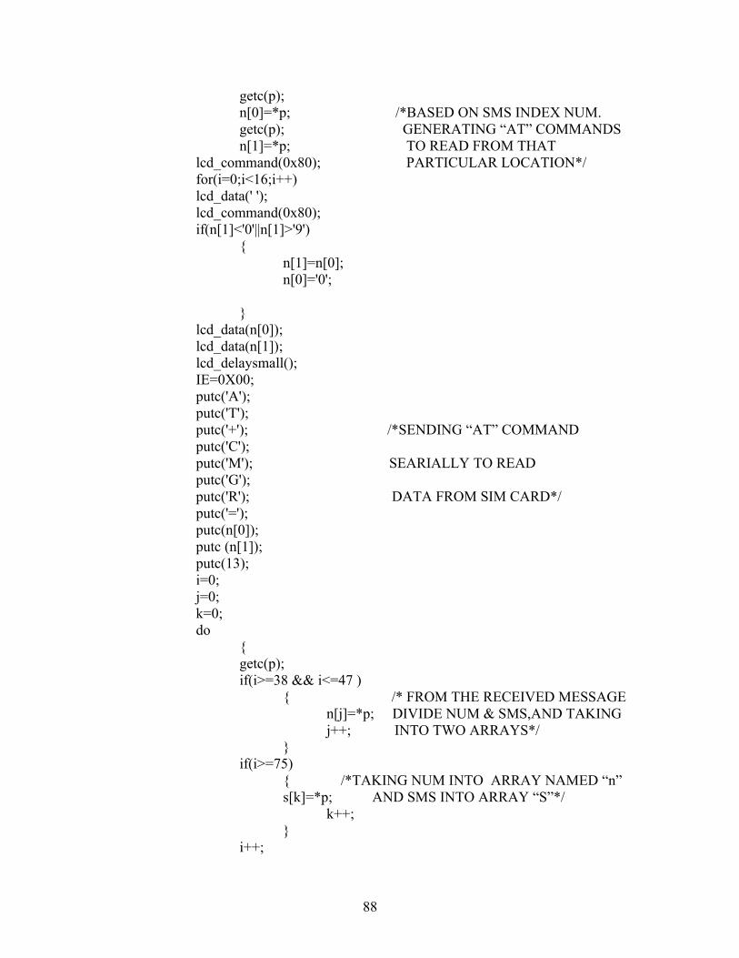
getc(p);n[0]=*p; /*BASED ON SMS INDEX NUM. getc(p); GENERATING “AT” COMMANDSn[1]=*p; TO READ FROM THAT
lcd_command(0x80); PARTICULAR LOCATION*/for(i=0;i<16;i++)lcd_data(' ');lcd_command(0x80);if(n[1]<'0'||n[1]>'9')
{n[1]=n[0];n[0]='0';
}lcd_data(n[0]);lcd_data(n[1]);lcd_delaysmall();IE=0X00;putc('A');putc('T');putc('+'); /*SENDING “AT” COMMAND putc('C');putc('M'); SEARIALLY TO READputc('G');putc('R'); DATA FROM SIM CARD*/putc('=');putc(n[0]);putc (n[1]);putc(13);i=0;j=0;k=0;do
{getc(p);if(i>=38 && i<=47 )
{ /* FROM THE RECEIVED MESSAGE n[j]=*p; DIVIDE NUM & SMS,AND TAKINGj++; INTO TWO ARRAYS*/
}if(i>=75)
{ /*TAKING NUM INTO ARRAY NAMED “n” s[k]=*p; AND SMS INTO ARRAY “S”*/
k++;}
i++;
88

}while(*p!='$'); /* “$” THIS SYMBOL IS TO CHECK s[k-1]=0; THE MESSAGE ENDING*/for(i=0;i<j;i++)
lcd_data(n[i]);lcd_command(0xc0);for(i=0;i<16;i++) /*SENDING INTIASTION COMMANDS lcd_data(' '); TO LCD*/lcd_command(0xc0);for(i=0;i<k;i++)
lcd_data(s[i]);if(strcmp(on,n)==0) /*COMPARING STRING FOR VALID
NUM OR NOT*/{
lcd_command(0x80);for(i=0;i<16;i++)lcd_data(' ');lcd_command(0x80);lcd_data('S');lcd_data('M'); /* IF NUM VALIDS DISPLAY lcd_data('S'); ON LCD AS SMS NUM VALID*/lcd_data(' ');lcd_data('N');lcd_data('U');lcd_data('M');lcd_data(' ');lcd_data('V');
}else
{lcd_command(0x80);for(i=0;i<16;i++)lcd_data(' ');lcd_command(0x80); /*IF NUM INVALID DISPLAY lcd_data('S'); ON LCD AS SMS NUM. INVALID*/lcd_data('M');lcd_data('S');lcd_data(' ');lcd_data('N');lcd_data('U');lcd_data('M');lcd_data(' ');lcd_data('I');lcd_data('V');continue;
}
89

if(strcmp(s,d1)==0) /*COMPARING THE SMS WITH THE { PROVIDED MESSAGE STRING &PERFORM
FAN=1; OPERATION ACCORDING TO MESSAGE*/display(); /*TO DISPLAY STATUS ON LCD*/sendback(); /*FUNCTION TO SEND BACK
STATUS OF DEVICE TO USER*/}
else if(strcmp(s,d2)==0) {
FAN=0;display();sendback();
}else if(strcmp(s,d3)==0)
{TV=1;display();sendback();
}else if(strcmp(s,d4)==0)
{ TV=0;
display();sendback();
} else if(strcmp(s,d5)==0)
{FREEZER=1;display();sendback();
}else if(strcmp(s,d6)==0)
{FREEZER=0;display();sendback();
}else if(strcmp(s,d7)==0)
{COOLER=1;display();sendback();
}else if(strcmp(s,d8)==0)
{COOLER = 0;
90

display();sendback();
}else
{display1();sendback1();}
for(i=0;i<15;i++)s[i]=0;
}}
void display(void){
unsigned int i;lcd_command(0xc0);for(i=0;i<16;i++)lcd_data(' ');
lcd_command(0xc0);lcd_data('S');lcd_data('M'); /* IF SMS VALID DISPLAY ON LCD AS SMS VALID*/lcd_data('S');lcd_data(' ');lcd_data('V');lcd_data('A');lcd_data('L');lcd_data('I');lcd_data('D');
return;}void display1(void){unsigned int i;
lcd_command(0xc0);for(i=0;i<16;i++)lcd_data(' ');
lcd_command(0xc0);lcd_data('S');lcd_data('M');lcd_data('S');lcd_data(' '); /* IF SMS IS INVALID DISPLAY ON LCD AS lcd_data('I'); SMS INVALID*/lcd_data('N');lcd_data('V');
91

lcd_data('A');lcd_data('L');lcd_data('I');lcd_data('D');
return;}
void sendback(void){signed char a;unsigned char *p;IE=0X00;putc('A');putc('T');putc('+');putc('C');putc('M'); /*SENDING ACKNOWLEDGE THROUGH GSM MODEM TO USER putc('G'); ABOUT DEVICES STATUS AS SUCCESS*/putc('S');putc('=');putc(n[0]);putc(n[1]);putc(n[2]);putc(n[3]);putc(n[4]);putc(n[5]);putc(n[6]);putc(n[7]);putc(n[8]);putc(n[9]);putc(13);do{getc(p);a=*p;}while(a!='>'); /*IF DEVICE FUNCTIONS THEN DISPLAY ON LCD AS SUCCESS*/putc('S');putc('U');putc('C');putc('C');putc(26);IE=0X81;return;}void sendback1(void)
92

{signed char a;unsigned char *p;IE=0X00;putc('A');putc('T');putc('+');putc('C');putc('M');putc('G');putc('S');putc('=');putc(n[0]);putc(n[1]);putc(n[2]); /*SENDING ACKNOWLEDGE TO USER THROUGH putc(n[3]); GSM MODEM ABOUT UNSUCESSFUL OPERATION*/putc(n[4]);putc(n[5]);putc(n[6]);putc(n[7]);putc(n[8]);putc(n[9]);putc(13);do{getc(p);a=*p;}while(a!='>');putc('U');putc('N');putc('S');putc('U');putc('C');putc('C');putc(26);
return;}
/*LCD CODE*/
#include<lcdheader.h>#include<reg52.h>#define lcd_port P0
93

void lcd_command(unsigned char command) /*CONFIGURING TO WORK AS { COMMAND MODE*/lcd_port=command;RS=0;RW=0;EN=1;EN=0;lcd_delaysmall();}
void lcd_data(unsigned char lcddata) /*CONFIGURING WORK AS { DATA MODE*/lcd_port=lcddata;RS = 1;RW = 0;EN = 1;EN = 0;lcd_delaysmall(); /*SMALL DELAY 40MILLI SECONDS*/}
void lcd_delaybig(void){ /* BIG DELAY OF 100MILLISECONDS*/unsigned int i,j;for(i=0;i<0x8888;i++)
{j++;}
}
void lcd_delaysmall(void){unsigned int i;for(i=0;i<5000;i++){}}
void lcd_init(){
lcd_delaybig();lcd_command(0x38);lcd_command(0x38);lcd_command(0x38);
94
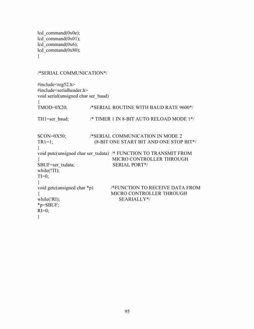
lcd_command(0x0e);lcd_command(0x01);lcd_command(0x6);lcd_command(0x80);}
/*SERIAL COMMUNICATION*/
#include<reg52.h>#include<serialheader.h>void serial(unsigned char ser_baud){TMOD=0X20; /*SERIAL ROUTINE WITH BAUD RATE 9600*/
TH1=ser_baud; /* TIMER 1 IN 8-BIT AUTO RELOAD MODE 1*/
SCON=0X50; /*SERIAL COMMUNICATION IN MODE 2 TR1=1; (8-BIT ONE START BIT AND ONE STOP BIT*/}void putc(unsigned char ser_txdata) /* FUNCTION TO TRANSMIT FROM { MICRO CONTROLLER THROUGH SBUF=ser_txdata; SERIAL PORT*/while(!TI);TI=0;}void getc(unsigned char *p) /*FUNCTION TO RECEIVE DATA FROM { MICRO CONTROLLER THROUGH while(!RI); SEARIALLY*/*p=SBUF;RI=0;}
95

CONCLUSION
When we send SMS to the SIM card number which is in the GSM modem, after
receiving the SMS GSM modem sends, Index number [Memory location in SIM card] as
response to the microcontroller unit. Based on the index number we have generated
attention commands (AT + CMGR) and send them serially to modem to get the message.
After receiving the message we have to check for the number, whether it is valid or
invalid. If the number is valid, based on contents or commands stored in the message we
will control the devices using some microcontroller to which some hardware components
are interfaced to control the devices.
The hardware components used in this project are ULN2003 I.C, Electromechanical
switches (Relays), diodes, Capacitors, resistors, MAX232 IC for serial communication,
LCD,LEDs,GSM modem (ANALOGIC company name), AT89s52 micro controller,3bd
Antenna,DB 9 connector, power supply of 5V for micro controller board and 9V for
GSM modem.
• PCB size is 10x12 cm.
• 2200 bytes of software used.
• Embedded C software
• Tools used is Keil uv2 IDE
96

sl.no. INPUT FORMAT OUT PUT DISPLAY ON
LCD1 1234fan on$ Device fan on, LED of fan
will glow.
Fan on
2 1234fan off$ Device fan off, LED of fan
will turn off if it is already
on.
Fan off
3 1234tv on$ Device tv on, LED of fan
will glow.
Tv on
4 1234tv off$ Device tv off, LED of tv
will turn off if it is already
on.
Tv off
5 1234freezer on$ Device freezer on, LED of
freezer will glow
Freezer on
6 1234freezer off$ Device freezer off, LED of
freezer will turn off if it is
already on.
Freezer off
7 1234ac on$ Device ac on, LED of ac
will glow.
Ac on
8 1234ac off$ Device ac off, LED of ac
will turn off if it is already
on.
Ac off
9 1234all on$ All devices will on,LEDs of
all devices will glow
All on
10 1234all off$ All devices will off,LEDs of
all devices will turn off
All off
Table c.1: Practical Inputs and Outputs
In the table “1234device on$” is the format of SMS to be sent to GSM modem .in that
“1234” is the password of the format and “$” symbol represents end of the SMS.
Here other than the above said format of SMS is received then it simply displays on LCD
as invalid SMS.
97

After performing operation as per given SMS, it will send acknowledge to SMS sent
number about status of operation.
ADVANTAGES
• GSM providers are available almost in many countries
• We can control the home appliances by sending a SMS to programmed home
automation kit with coded instructions by the authenticated programmer
simultaneously we will get a feedback and the status of the device. Since we have an
option of Roaming Service provided by the GSM service providers hence we can get
SMS at any place on the earth.
• We can Switch ON/OFF the devices by sending a SMS from any place in the
world.
• It is cheaper when compared to the other type of automation system.
• It is more effective when compared to the other type of automation system.
• It is easy to change the system’s action according to change in situation.
DISADVANTAGES
• It requires a continuous electrical power supply for its proper working
• We have to continuously recharge the GSM SIMCARD.
• Maintenance cost is high i.e. service charges are more per SMS.
• If the SIM gets damaged we need to reprogram with other number for security
purposes because the cost depends on the service provider.
98

FUTURE ASPECTS
• Some of the pins of the microcontroller are left unused & hence can be used in the
future by defining the functions.
• We can control many devices by increasing the ULN2003 IC’s (which are
connected to the microcontroller).
• We may implement this project for the industrial purposes also.
• By interfacing ADC0808 to microcontroller we may achieve security in case of
1. fire accidents
2. poisonous gases
This system will act according to the parameters given by the user.
IMPLEMENTATION OF THIS PROJECT
This project proposal is under consideration of Govt. of Andhra Pradesh for central street
lightening in Nellore District.
BIBILIOGRAPHY
99

1. www.alldatasheet.com
2. www.8051.com
3. www.wavecomm.com
4. www.atmel.com
5.www.keilsoftware.com
6. Muhammad Ali Mazidi, J.G.Mazidi,”The 8051 Micro Controller
& Embedded Systems” PHI Series, 2005.
100