Embed Size (px)
Citation preview

Introduction to Fast Analytical Techniques:Application to Small-Signal Modeling
Christophe Basso Technical FellowChristophe Basso – Technical Fellow
IEEE Senior Member
Public Information
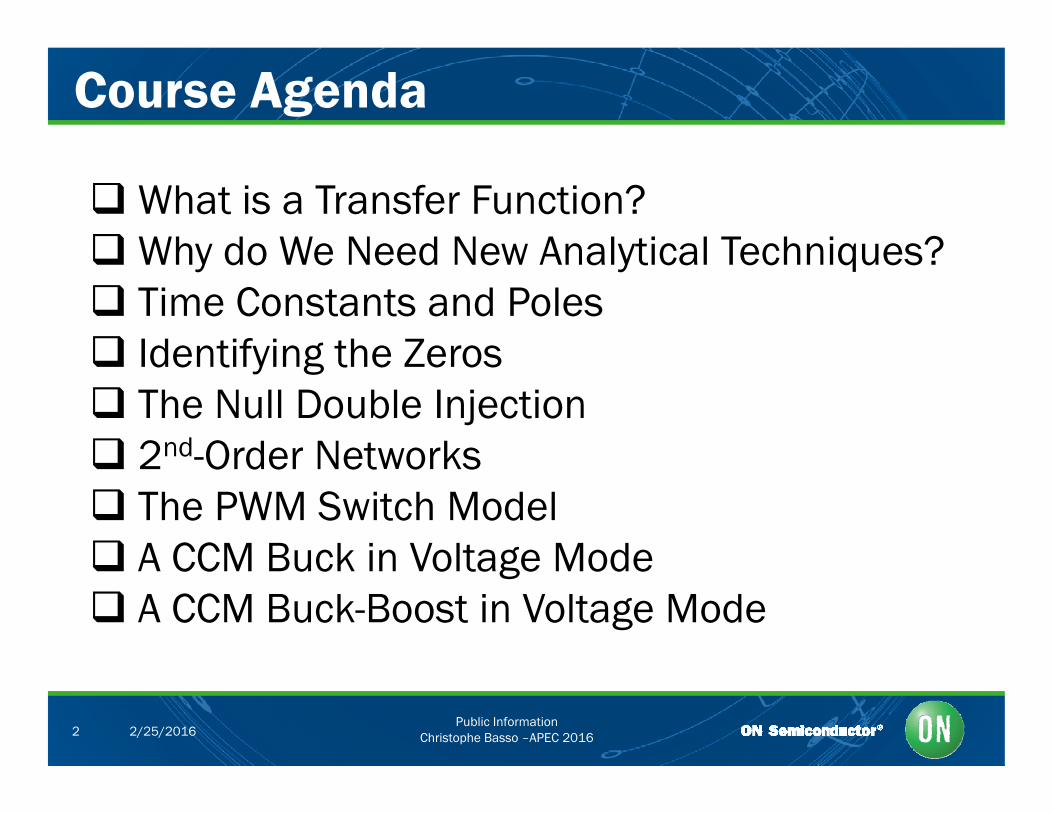
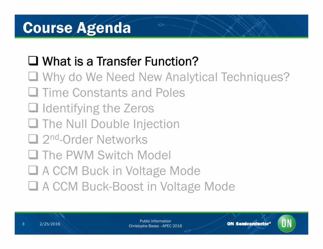
Course Agenda
What is a Transfer Function? Why do We Need New Analytical Techniques? Why do We Need New Analytical Techniques? Time Constants and Poles Identifying the Zeros Identifying the Zeros The Null Double Injection 2nd-Order Networks 2 -Order Networks The PWM Switch Model A CCM Buck in Voltage Mode A CCM Buck in Voltage Mode A CCM Buck-Boost in Voltage Mode
Public InformationChristophe Basso –APEC 20162 2/25/2016
Course Agenda
What is a Transfer Function? Why do We Need New Analytical Techniques? Why do We Need New Analytical Techniques? Time Constants and Poles Identifying the Zeros Identifying the Zeros The Null Double Injection 2nd-Order Networks 2 -Order Networks The PWM Switch Model A CCM Buck in Voltage Mode A CCM Buck in Voltage Mode A CCM Buck-Boost in Voltage Mode
Public InformationChristophe Basso –APEC 20163 2/25/2016
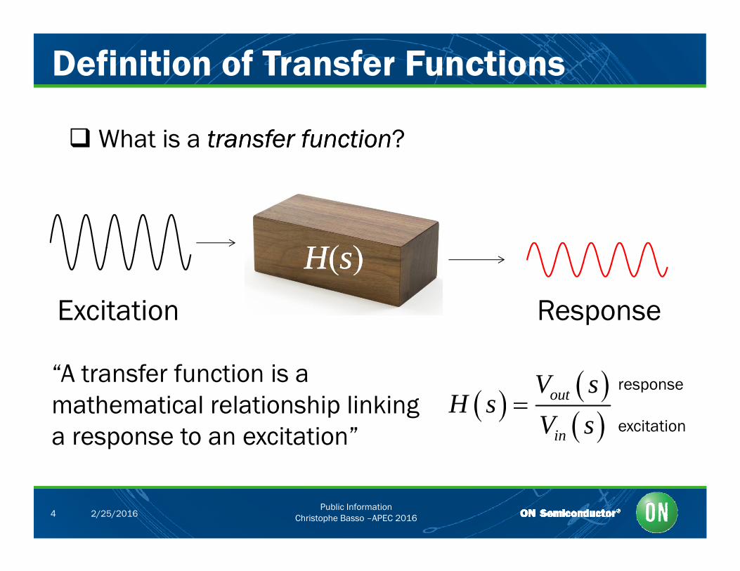
Definition of Transfer Functions
What is a transfer functiontransfer function?
HH(( ))Excitation Response
HH((ss))p
“A transfer function is a outV s response
mathematical relationship linking a response to an excitation”
out
in
H sV s
excitation
Public InformationChristophe Basso –APEC 20164 2/25/2016
Six Types of Transfer Functions
Transfer function can involve signals at different places
Response Response
out
in
V sH s
V s inV s outV s
out
in
I sH s
I s inI s outI s
Excitation Excitation
Response Response
Voltage gain Current gain
Excitation
out
in
I sH s
V s outI s inV s
out
in
V sH s
I s outV s inI s
Response Response
Transfer admittanceor transadmittance
Transimpedance
Excitation Excitation
Public InformationChristophe Basso –APEC 20165 2/25/2016
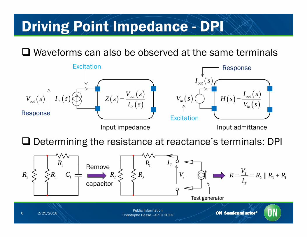
Driving Point Impedance - DPI
Waveforms can also be observed at the same terminalsExcitation Response
outV sZ s
I s inI s outV s
outI s
H sV s
inV s
outI s
inI s
Input impedance
Response inV s
Input admittanceExcitation
Determining the resistance at reactance’s terminals: DPI
IRRRemove
capacitor
TI
TV1R
2R 3R 2 3 1||T
T
VR R R R
I
1R
2R 3R 1C
Public InformationChristophe Basso –APEC 20166 2/25/2016
Test generator
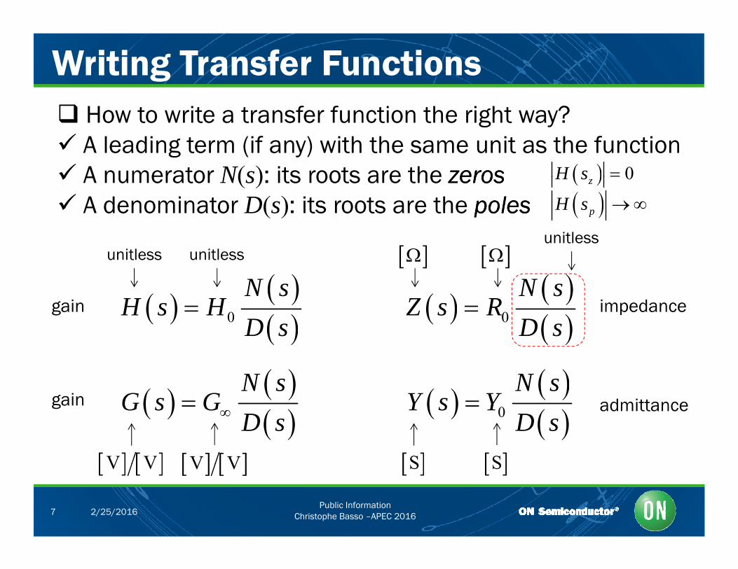
Writing Transfer Functions How to write a transfer function the right way? A leading term (if any) with the same unit as the function A numerator N(s): its roots are the zeroszeros 0H s A numerator N(s): its roots are the zeroszeros A denominator D(s): its roots are the polespoles
i l i l unitless
0zH s
pH s
0
N sH s H
D
0
N sZ s R
D
unitless unitless
gain impedance 0 D s 0 D s
N s N s
G s GD s
0Y s YD s
S S V V V V
gain admittance
Public InformationChristophe Basso –APEC 20167 2/25/2016
S S V V V V

Course Agenda
What is a Transfer Function? Why do We Need New Analytical Techniques? Why do We Need New Analytical Techniques? Time Constants and Poles Identifying the Zeros Identifying the Zeros The Null Double Injection 2nd-Order Networks 2 -Order Networks The PWM Switch Model A CCM Buck in Voltage Mode A CCM Buck in Voltage Mode A CCM Buck-Boost in Voltage Mode
Public InformationChristophe Basso –APEC 20168 2/25/2016
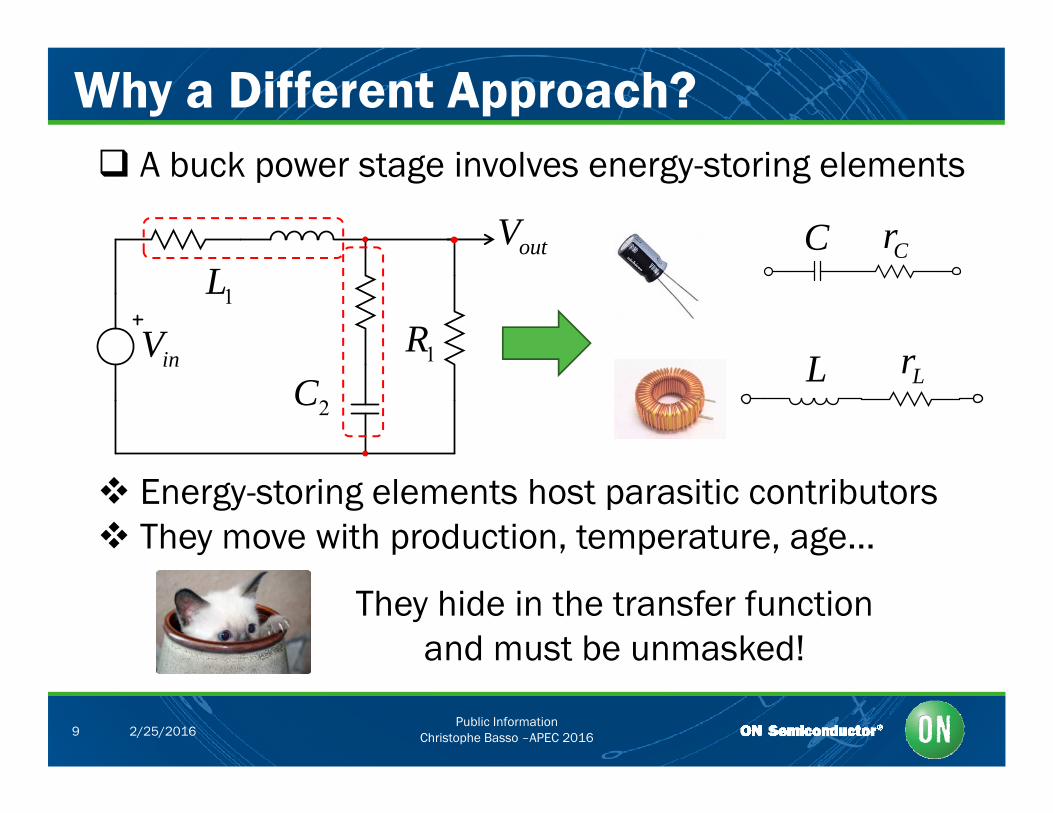
Why a Different Approach? A buck power stage involves energy-storing elements
C CroutV C
1L
iV 1R
out
L Lr2C
inV 1
Energy-storing elements host parasitic contributors They move with production, temperature, age...
They hide in the transfer functionand must be unmasked!
Public InformationChristophe Basso –APEC 20169 2/25/2016
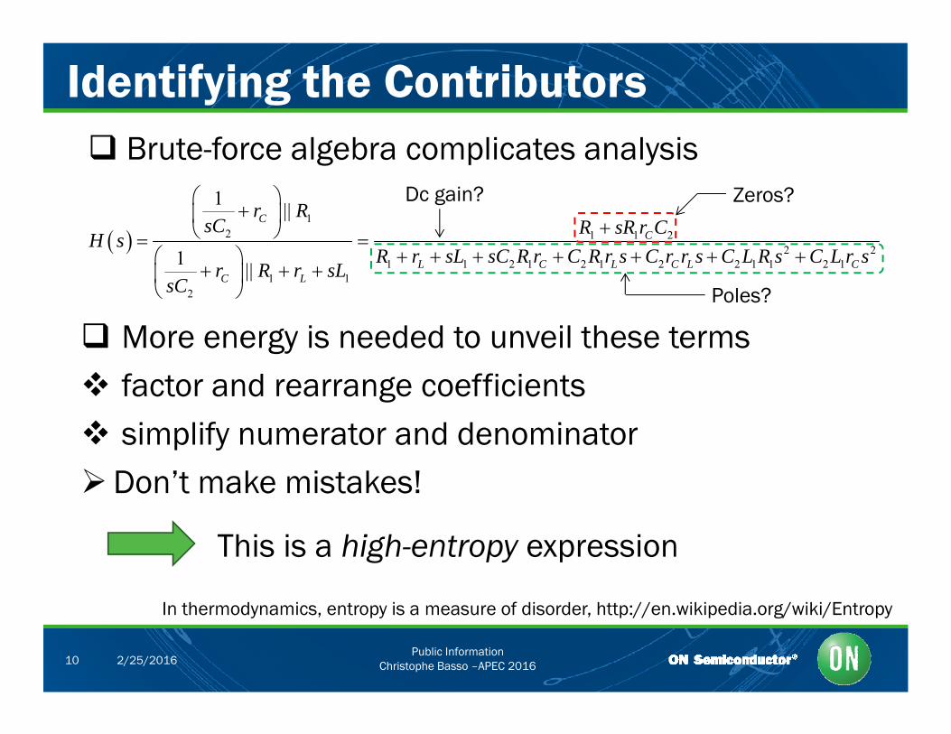
Identifying the Contributors
11 ||Cr R
sC R sR r C
Brute-force algebra complicates analysisZeros?Dc gain?
2 1 1 22 2
1 1 2 1 2 1 2 2 1 1 2 11 1
2
1 ||
C
L C L C L CC L
sC R sR r CH s
R r sL sC R r C R r s C r r s C L R s C L r sr R r sL
sC
Poles?
More energy is needed to unveil these terms factor and rearrange coefficients simplify numerator and denominatorDon’t make mistakes!
This is a high-entropy expression
Public InformationChristophe Basso –APEC 201610 2/25/2016
In thermodynamics, entropy is a measure of disorder, http://en.wikipedia.org/wiki/Entropy
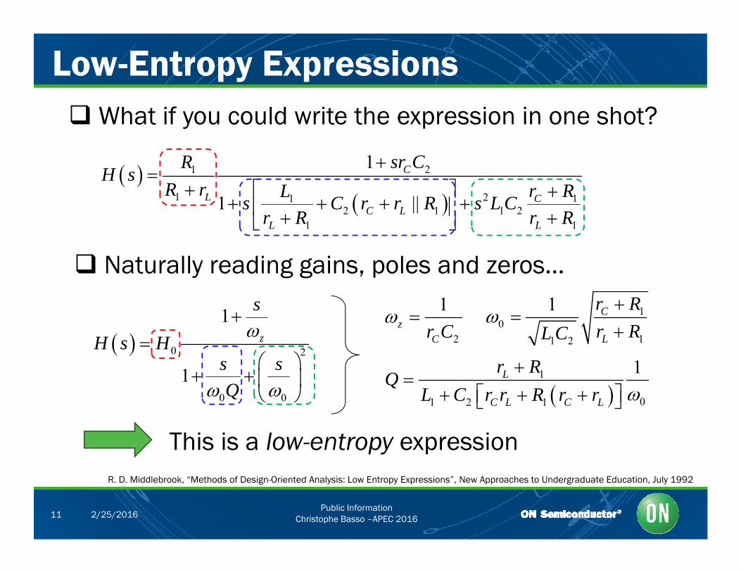
Low-Entropy Expressions
21 1 Csr CRH s
What if you could write the expression in one shot?
1 2 11
2 1 1 21 1
1 ||L CC L
L L
H sR r r RLs C r r R s L C
r R r R
1 s
Naturally reading gains, poles and zeros…1 1
01 Cr R
0 2
0 0
1
zH s Hs sQ
2z
Cr C 0
11 2 Lr RL C
1 1Lr R
QL C r r R r r
0 0Q 01 2 1C L C LL C r r R r r
This is a low-entropy expression
Public InformationChristophe Basso –APEC 201611 2/25/2016
R. D. Middlebrook, “Methods of Design-Oriented Analysis: Low Entropy Expressions”, New Approaches to Undergraduate Education, July 1992
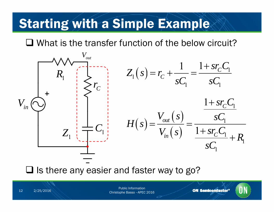
Starting with a Simple Example What is the transfer function of the below circuit?
11 sr CoutV
1RCr
11
1 1
11 CC
sr CZ s r
sC sC
inV
1
1
1 C
out
sr CV s sC
1C
1
11
1out
Cin
sCH s
sr CV s RsC
1Z1sC
Is there any easier and faster way to go?
Public InformationChristophe Basso –APEC 201612 2/25/2016
Is there any easier and faster way to go?
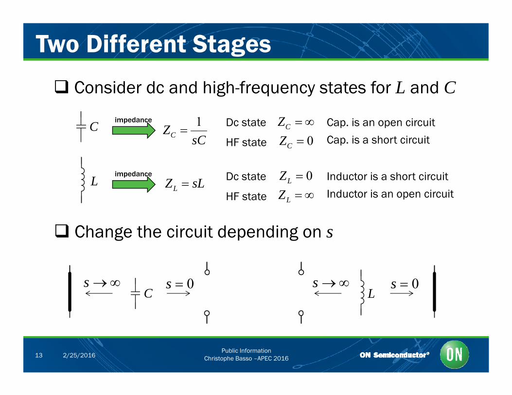
Two Different Stages
Consider dc and high-frequency states for L and C
C impedance 1 Dc state Z Cap is an open circuitC p 1CZ
sC Dc state
HF stateCZ
0CZ Cap. is an open circuit
Cap. is a short circuit
impedance D 0Z I d i h i iLimpedance
LZ sL Dc state
HF state
0LZ
LZ Inductor is a short circuit
Inductor is an open circuit
Change the circuit depending on s
C L0s 0s s s
Public InformationChristophe Basso –APEC 201613 2/25/2016
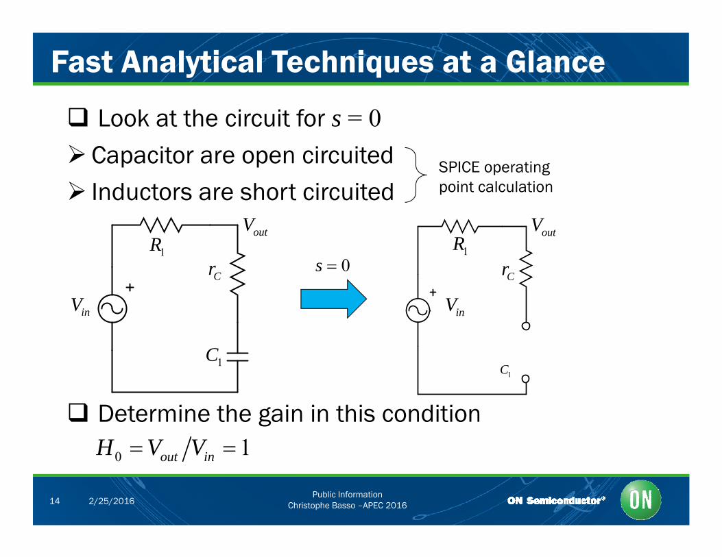
Fast Analytical Techniques at a Glance
Look at the circuit for s = 0Capacitor are open circuited SPICE operating
Inductors are short circuited
RoutV
RoutV
p gpoint calculation
0s
inV
1RCr
1RCr
inVin
1C
in
1C
Determine the gain in this condition
0 1t iH V V
Public InformationChristophe Basso –APEC 201614 2/25/2016
0 1out inH V V
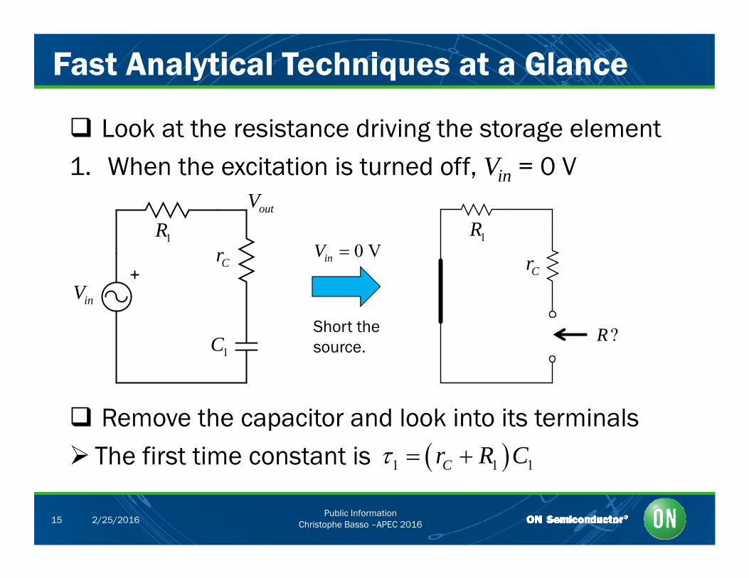
Fast Analytical Techniques at a Glance
Look at the resistance driving the storage element1. When the excitation is turned off, Vin = 0 Vin
0 VV 1R
r
outV
1R0 VinV
inVCr
Cr
Short the1C ?RShort the
source.
Remove the capacitor and look into its terminals The first time constant is 1 1 1Cr R C
Public InformationChristophe Basso –APEC 201615 2/25/2016
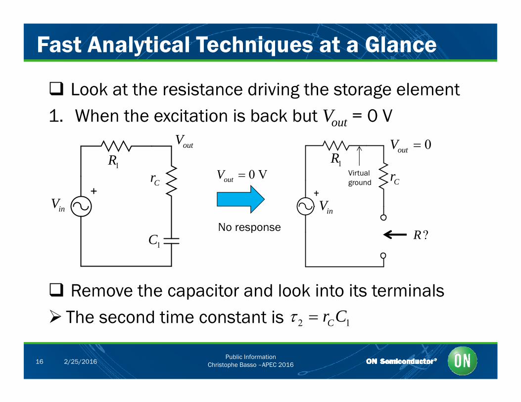
Fast Analytical Techniques at a Glance
Look at the resistance driving the storage element1. When the excitation is back but Vout = 0 Vout
0 VV 1R
r
outV1R
r
0outV
Virtual0 VoutV
inVCr
No response
Cr
inV
ground
1C ?RNo response
Remove the capacitor and look into its terminals The second time constant is 2 1Cr C
Public InformationChristophe Basso –APEC 201616 2/25/2016
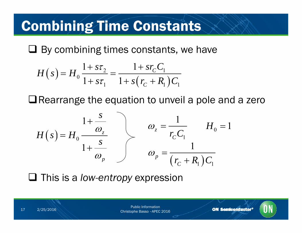
Combining Time Constants By combining times constants, we have
12 11 Csr CsH s H
01 1 11 1 C
H s Hs s r R C
Rearrange the equation to unveil a pole and a zeroRearrange the equation to unveil a pole and a zero
1 s
1
z C 0 1H
0
1
z
p
H s Hs
1z
Cr C
1
p r R C
0
p 1 1Cr R C
This is a low-entropy expression
Public InformationChristophe Basso –APEC 201617 2/25/2016
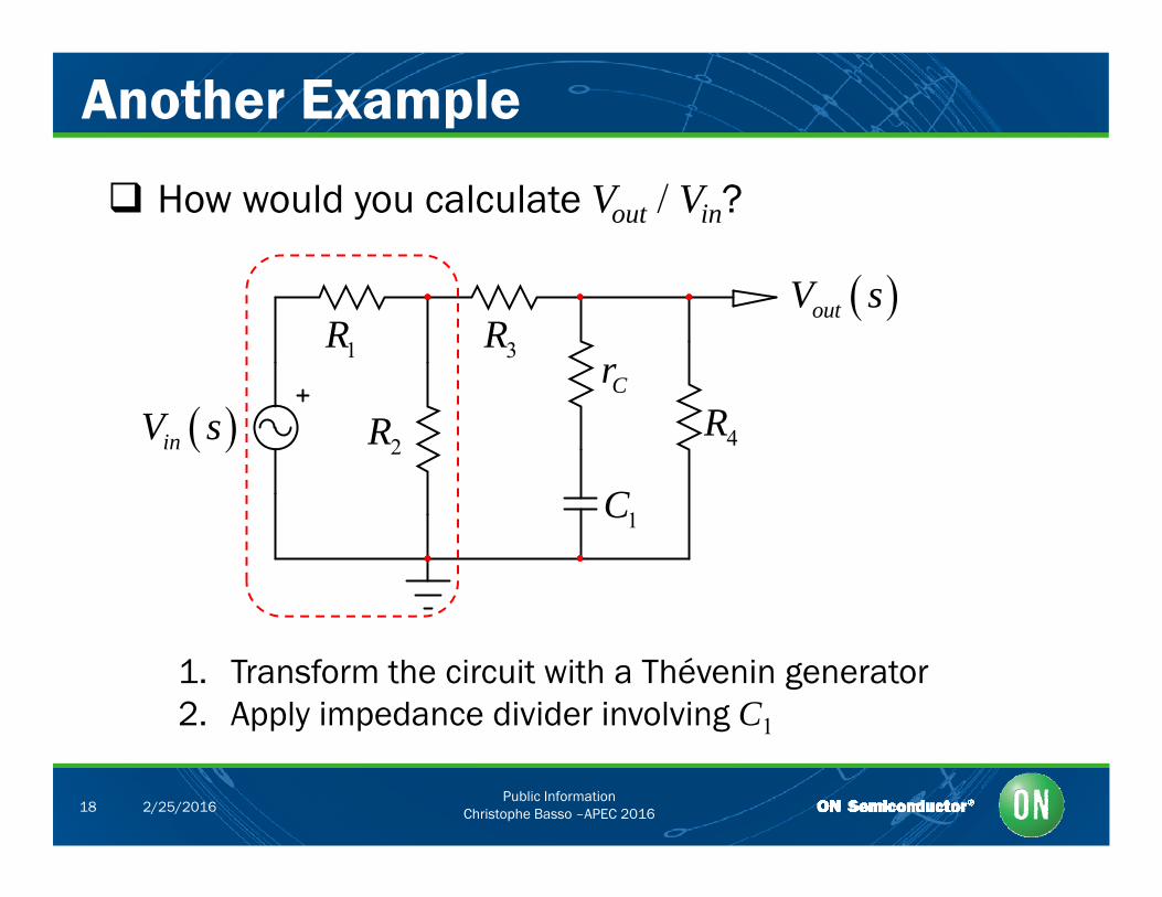
Another Example
How would you calculate Vout / Vin?
1R 3R
Cr
outV s
2RC
C
4R inV s
1C
1. Transform the circuit with a Thévenin generator2. Apply impedance divider involving C1
Public InformationChristophe Basso –APEC 201618 2/25/2016
g 1
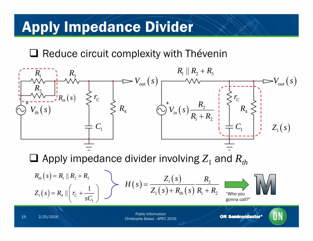
Apply Impedance Divider
Reduce circuit complexity with Thévenin
1 2 3||R R R1R 3R
R
outV s outV s1 2 3
Cr
1R
2R3R
Cr thR s
thV s 2
1 2in
RV s
R R
1C
4R
1C
4R
1Z s
Apply impedance divider involving Z1 and Rth
1 2
1 1 2th
Z s RH s
Z s R s R R
1 41|| CZ s R rC
1 2 3||thR s R R R
“Who you
Public InformationChristophe Basso –APEC 201619 2/25/2016
1 41
C sC gonna call?”
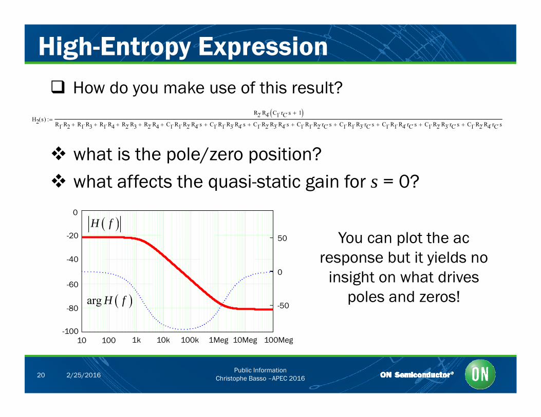
High-Entropy Expression
H2 s( )R2 R4 C1 rC s 1
R1 R2 R1 R3 R1 R4 R2 R3 R2 R4 C1 R1 R2 R4 s C1 R1 R3 R4 s C1 R2 R3 R4 s C1 R1 R2 rC s C1 R1 R3 rC s C1 R1 R4 rC s C1 R2 R3 rC s C1 R2 R4 rC s
How do you make use of this result?
what is the pole/zero position? what affects the quasi-static gain for s = 0? what affects the quasi-static gain for s = 0?
0
20 H f
You can plot the ac -20
-40
-60
0
50 You can plot the ac response but it yields no
insight on what drives
-80
-10010 100 1k 10k 100k 1Meg 10Meg 100Meg
-50 arg H f poles and zeros!
Public InformationChristophe Basso –APEC 201620 2/25/2016
10 100 1k 10k 100k 1Meg 10Meg 100Meg
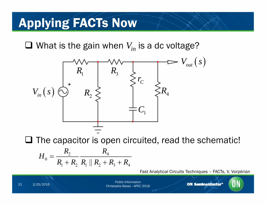
Applying FACTs Now
What is the gain when Vin is a dc voltage?
tV s1R
R
3RCr
R
outV s
V2R
1C
4R inV s
The capacitor is open circuited read the schematic! The capacitor is open circuited, read the schematic! 2 4
01 2 1 2 3 4||R R
HR R R R R R
Public InformationChristophe Basso –APEC 201621 2/25/2016
Fast Analytical Circuits Techniques – FACTs, V. Vorpérian
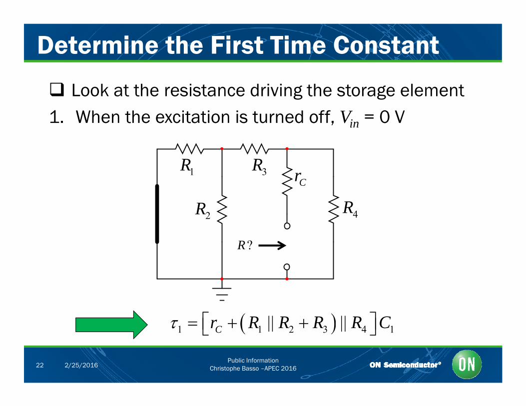
Determine the First Time Constant
Look at the resistance driving the storage element1. When the excitation is turned off, Vin = 0 Vin
1R 3R r
2RCr
4R
?R
1 1 2 3 4 1|| ||Cr R R R R C
Public InformationChristophe Basso –APEC 201622 2/25/2016
1 1 2 3 4 1|| ||C
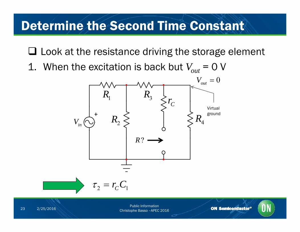
Determine the Second Time Constant
Look at the resistance driving the storage element1. When the excitation is back but Vout = 0 Vout
1R 3R r
0outV
2RCr
4RinV
Virtualground
?R
2 1Cr C
Public InformationChristophe Basso –APEC 201623 2/25/2016
2 1C
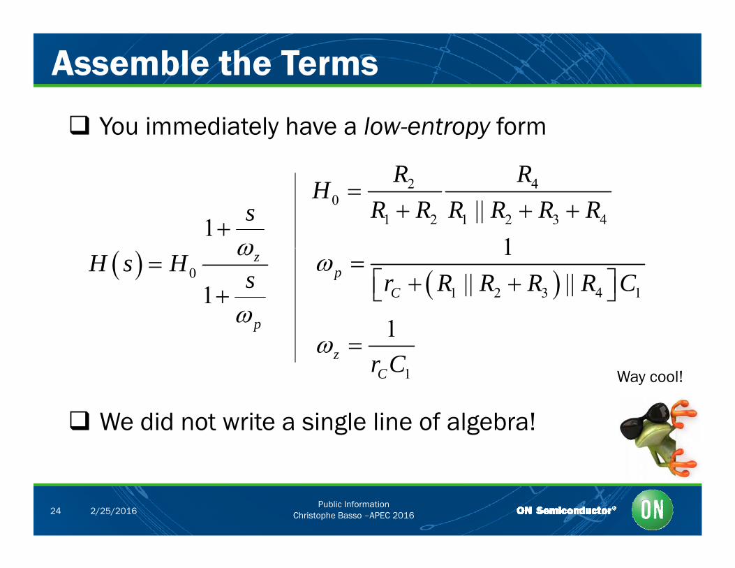
Assemble the Terms
You immediately have a low-entropy form
R R
1 s
2 40
1 2 1 2 3 4||R R
HR R R R R R
1 0
1
zH s Hs
1
1 2 3 4 1
1|| ||p
Cr R R R R C
p
1
1z
Cr C
Way cool!
We did not write a single line of algebra!
Public InformationChristophe Basso –APEC 201624 2/25/2016
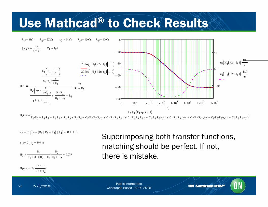
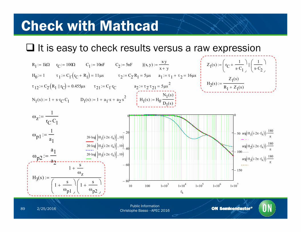
Use Mathcad® to Check ResultsR1 1k R2 22k rC 0.1 R3 150 R4 100
|| x y( )x y
x y C1 1F
40
20
0
50
20 log H1 i 2 fk 10 arg H1 i 2 fk 180
H s( )
R4 rC1
s C1
R4 rC1
s C1
R4 rC1
R2R1 R2 80
60
40
50
0
20 log H1 i 2 fk 10 20 log H2 i 2 fk 10
1
arg H2 i 2 fk 180
R4 rC s C1
R4 rC1
s C1
R1 R2
R1 R2 R3
H2 s( )R2 R4 C1 rC s 1
R R R R R R R R R R C R R R C R R R C R R R C R R C R R C R R C R R C R R
10 100 1 103 1 104 1 105 1 106 1 107 1 108100
fk
2 R1 R2 R1 R3 R1 R4 R2 R3 R2 R4 C1 R1 R2 R4 s C1 R1 R3 R4 s C1 R2 R3 R4 s C1 R1 R2 rC s C1 R1 R3 rC s C1 R1 R4 rC s C1 R2 R3 rC s C1 R2 R4 rC s
2 C1 rC R1 || R2 R3 || R4 91.812 s
1 C1 rC 100 nsSuperimposing both transfer functions,
1 C1 rC 100 ns
H0R4
R4 R1 || R2 R3
R2R1 R2 0.079
H1 s( ) H01 s 1
matching should be perfect. If not, there is mistake.
Public InformationChristophe Basso –APEC 201625 2/25/2016
H1 s( ) H0 1 s 2

Course Agenda
What is a Transfer Function? Why do We Need New Analytical Techniques? Why do We Need New Analytical Techniques? Time Constants and Poles Identifying the Zeros Identifying the Zeros The Null Double Injection 2nd-Order Networks 2 -Order Networks The PWM Switch Model A CCM Buck in Voltage Mode A CCM Buck in Voltage Mode A CCM Buck-Boost in Voltage Mode
Public InformationChristophe Basso –APEC 201626 2/25/2016
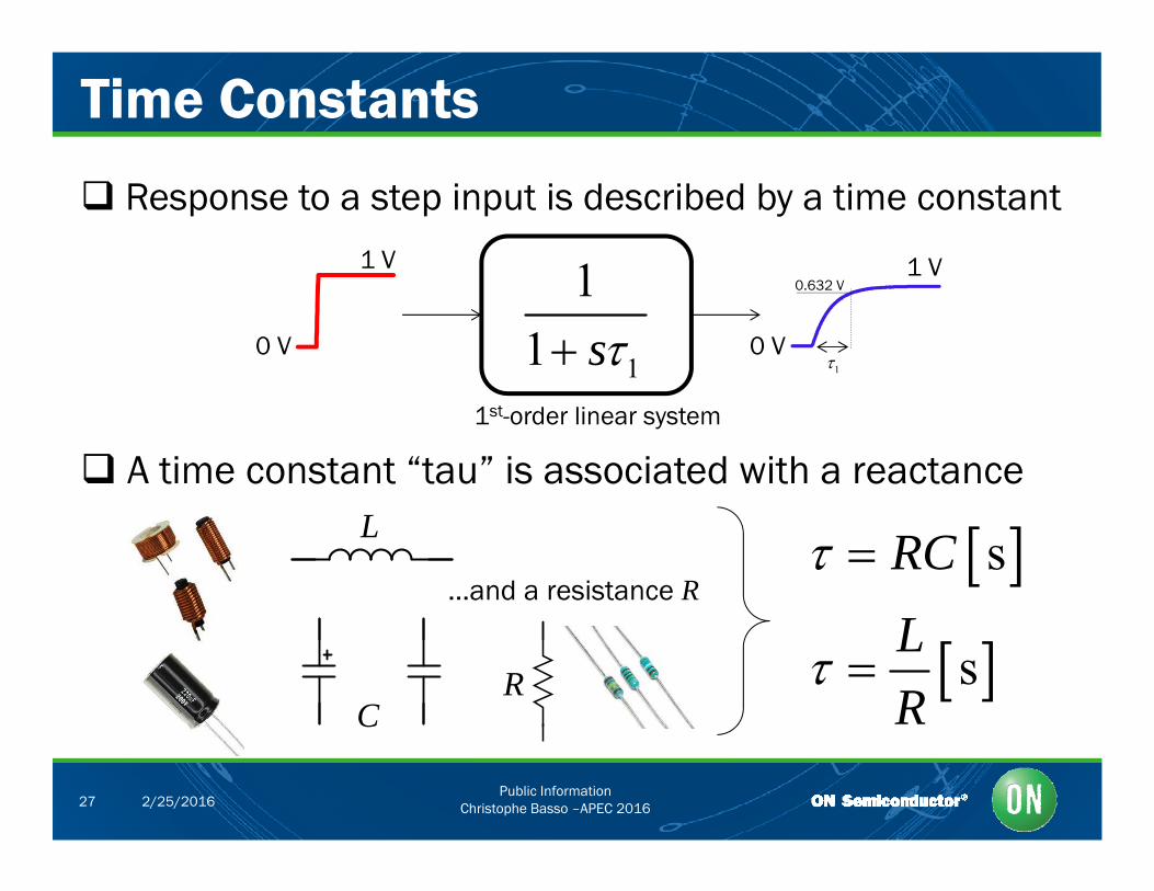
Time Constants
Response to a step input is described by a time constant
1 V 1 1 V
0 V1
11 s 0 V
0.632 V
1
A time constant “tau” is associated with a reactance1st-order linear system
…and a resistance R sRC
L
sLR
C
R
Public InformationChristophe Basso –APEC 201627 2/25/2016
C
Time-Domain Response
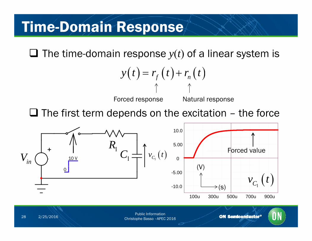
The time-domain response y(t) of a linear system is
fy t r t r t f ny t r t r t
Forced response Natural response
The first term depends on the excitation – the force10.0
inV1R
1C10 V 0
5.00Forced value
1Cv t(V)0
100u 300u 500u 700u 900u
-10.0
-5.00
1Cv t
(V)
(s)
Public InformationChristophe Basso –APEC 201628 2/25/2016
100u 300u 500u 700u 900u
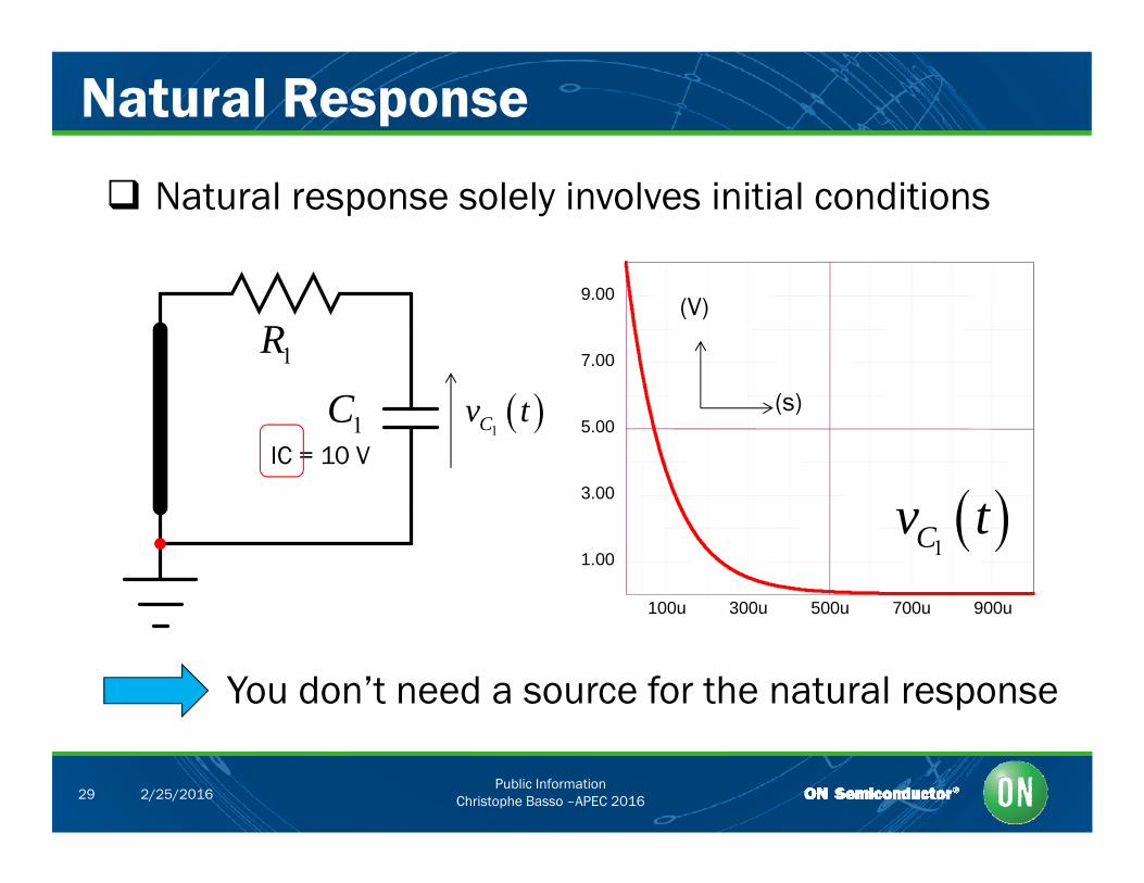
Natural Response
Natural response solely involves initial conditions
7.00
9.00(V)
1R
3.00
5.00
(s)1C
1Cv tIC = 10 V
100u 300u 500u 700u 900u
1.00
3.00 1Cv t
100u 300u 500u 700u 900u
You don’t need a source for the natural response
Public InformationChristophe Basso –APEC 201629 2/25/2016
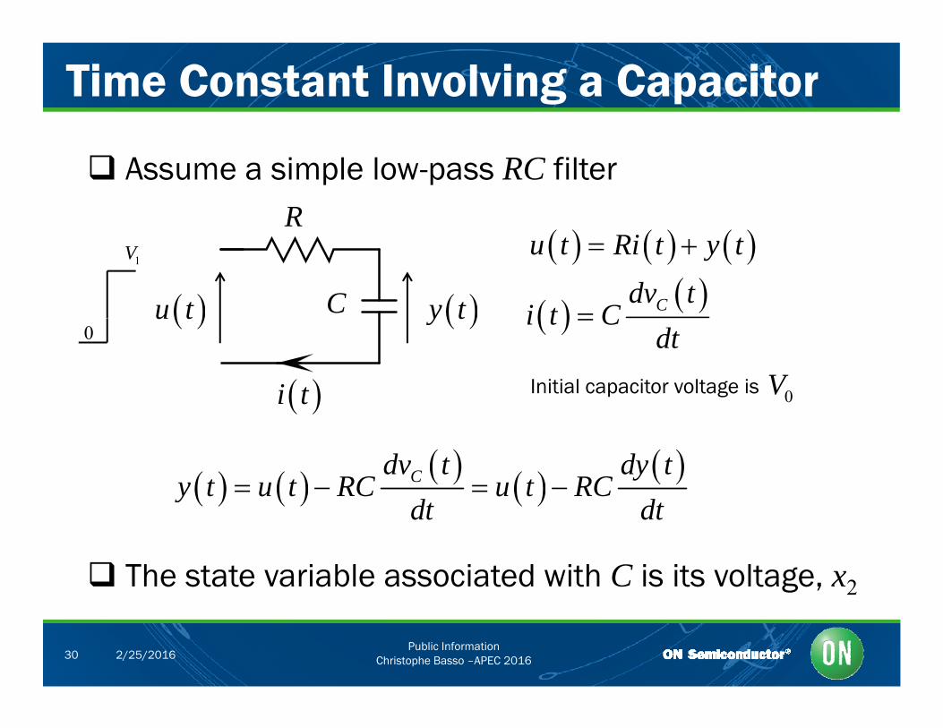
Time Constant Involving a Capacitor
R Assume a simple low-pass RC filter
C y t u t
u t Ri t y t
Cdv ti t C
1V
0 y t u t
i t
i t Cdt
Initial capacitor voltage is 0V
Cdv t dy ty t u t RC u t RC
d d y
dt dt
The state variable associated with C is its voltage, x2
Public InformationChristophe Basso –APEC 201630 2/25/2016
2
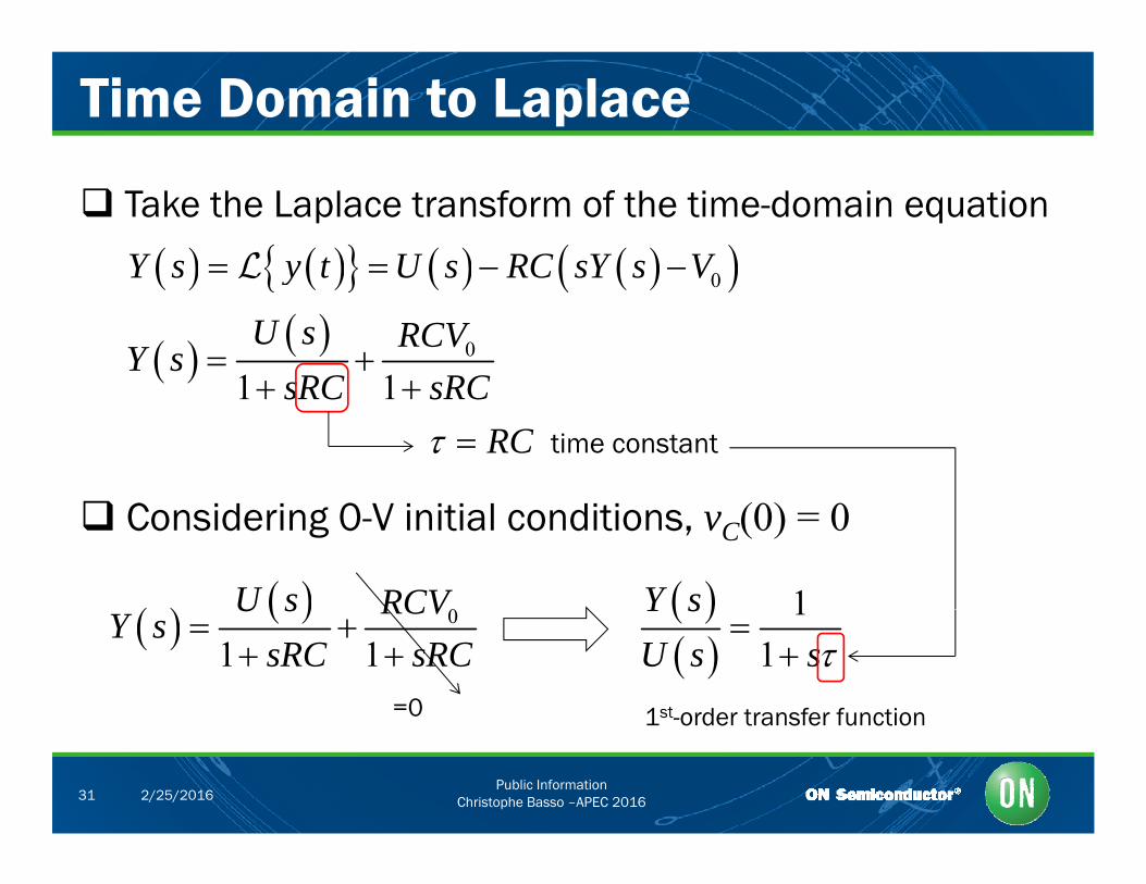
Time Domain to Laplace
0Y s y t U s RC sY s V
Take the Laplace transform of the time-domain equation
0Y s y t U s RC sY s V
0
1 1U s RCV
Y ssRC sRC
1 1sRC sRC
RC time constant
0U s RCV
Considering 0-V initial conditions, vC(0) = 0
1Y s 0
1 1U s RCV
Y ssRC sRC
11
Y sU s s
1st-order transfer function=0
Public InformationChristophe Basso –APEC 201631 2/25/2016
1 order transfer function
Forced and Natural Responses
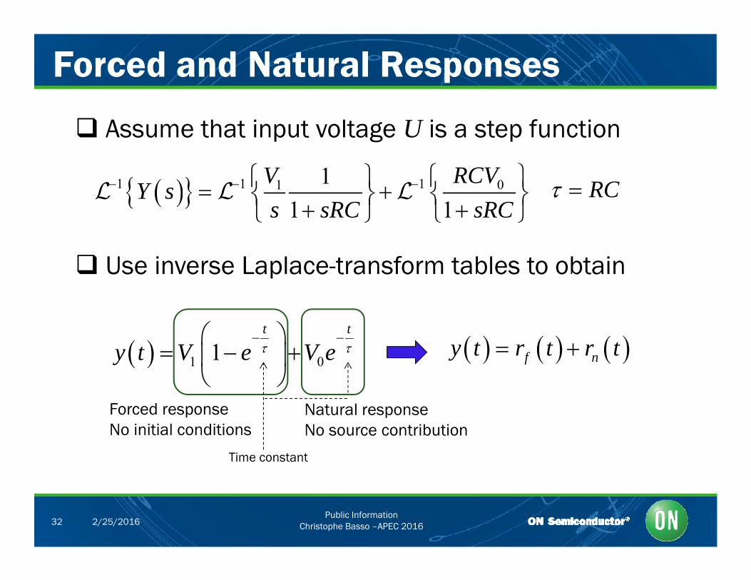
Assume that input voltage U is a step function
1 1 1 01 1 RCVV 1 1 1 01 11 1
RCVVY s
s sRC sRC
RC
Use inverse Laplace-transform tables to obtain
t t 1 01t t
y t V e V e
f ny t r t r t
Natural responseNo source contribution
Forced responseNo initial conditions
Time constant
Public InformationChristophe Basso –APEC 201632 2/25/2016
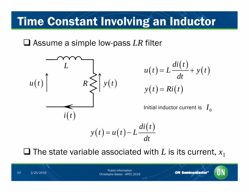
Time Constant Involving an Inductor
Assume a simple low-pass LR filter
R
L
y t u t
di tu t L y t
dt
R y t u t y t Ri t
Initial inductor current is I i t
Initial inductor current is 0I
di ty t u t L y t u t L
dt
The state variable associated with L is its current, x1
Public InformationChristophe Basso –APEC 201633 2/25/2016
1

Laplace Transform
Y U L I I Y sI
Take the Laplace transform of the time-domain equation
0Y s y t U s L sI s I I s
R
Y sY U L I
0U s LI
Y 0Y s U s L s I
R
0
1 1Y s
L Ls sR R
LR
0U s LI
Considering 0-A initial conditions, iL(0) = 0
1Y sTime constant 0
1 1
U s LIY s
L Ls sR R
11
Y sU s s
1st-order transfer function
Public InformationChristophe Basso –APEC 201634 2/25/2016
1 order transfer function=0
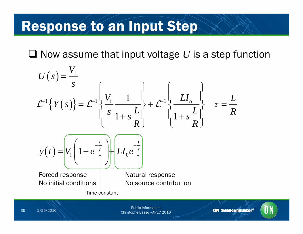
Response to an Input Step
1VU
Now assume that input voltage U is a step function
1VU s
s
1 1 11 1 oLIVY
L 1 1 11
1 1
oY sL Ls s sR R
R
1 01t t
y t V e LI e
Natural responseNo source contribution
Forced responseNo initial conditions
Public InformationChristophe Basso –APEC 201635 2/25/2016
Time constant
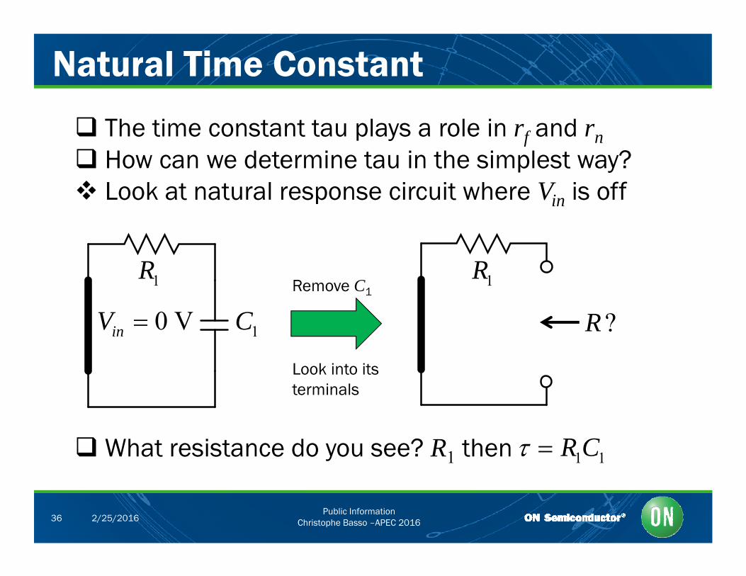
Natural Time Constant
The time constant tau plays a role in rf and rn How can we determine tau in the simplest way? Look at natural response circuit where Vin is off
1R
C0 VV Remove C1
1R
?R1C0 VinV
Look into itsterminals
?R
What resistance do you see? R1 then 1 1R C
Public InformationChristophe Basso –APEC 201636 2/25/2016
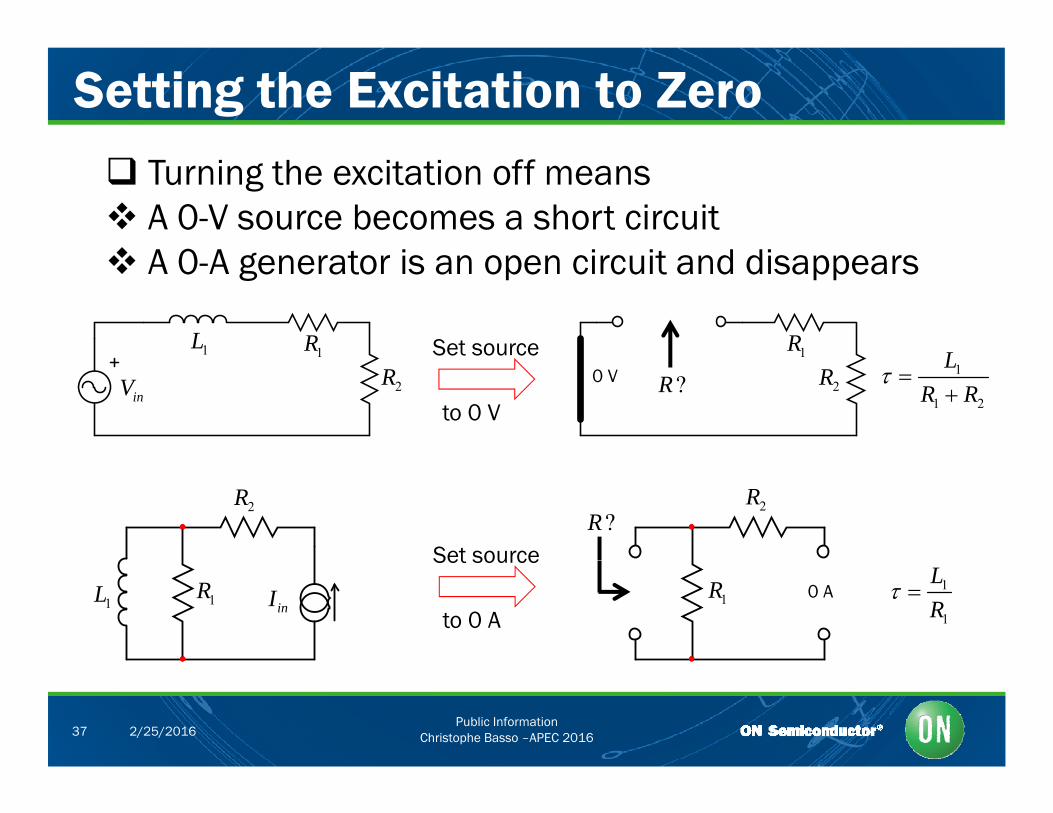
Setting the Excitation to Zero Turning the excitation off means A 0-V source becomes a short circuit A 0 A g t i i it d di A 0-A generator is an open circuit and disappears
1R1L 1RSet source L1
2RinV
1
2RSet sou ce
to 0 V?R
1
1 2
LR R
0 V
Set source
2R?R
2R
Set source
to 0 A1R
1LinI 1R 1
1
LR
0 A
Public InformationChristophe Basso –APEC 201637 2/25/2016
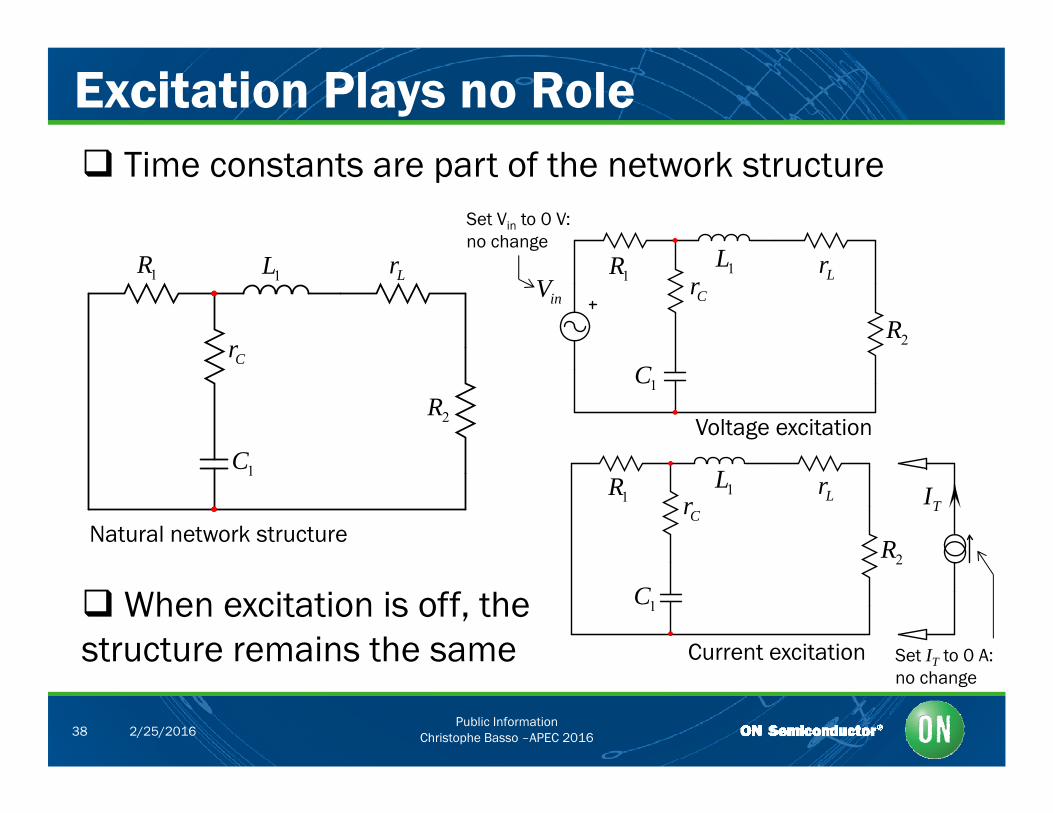
Excitation Plays no Role Time constants are part of the network structure
LSet Vin to 0 V:no change
1R
Cr
1L Lr 1RCr
1LLr
2RinV
Cr
C
2R1C
Voltage excitation
1C
Natural network structure
1RCr
1LLr
2R
TI
1C2
When excitation is off, thestructure remains the same Current excitation Set IT to 0 A:
Public InformationChristophe Basso –APEC 201638 2/25/2016
Tno change
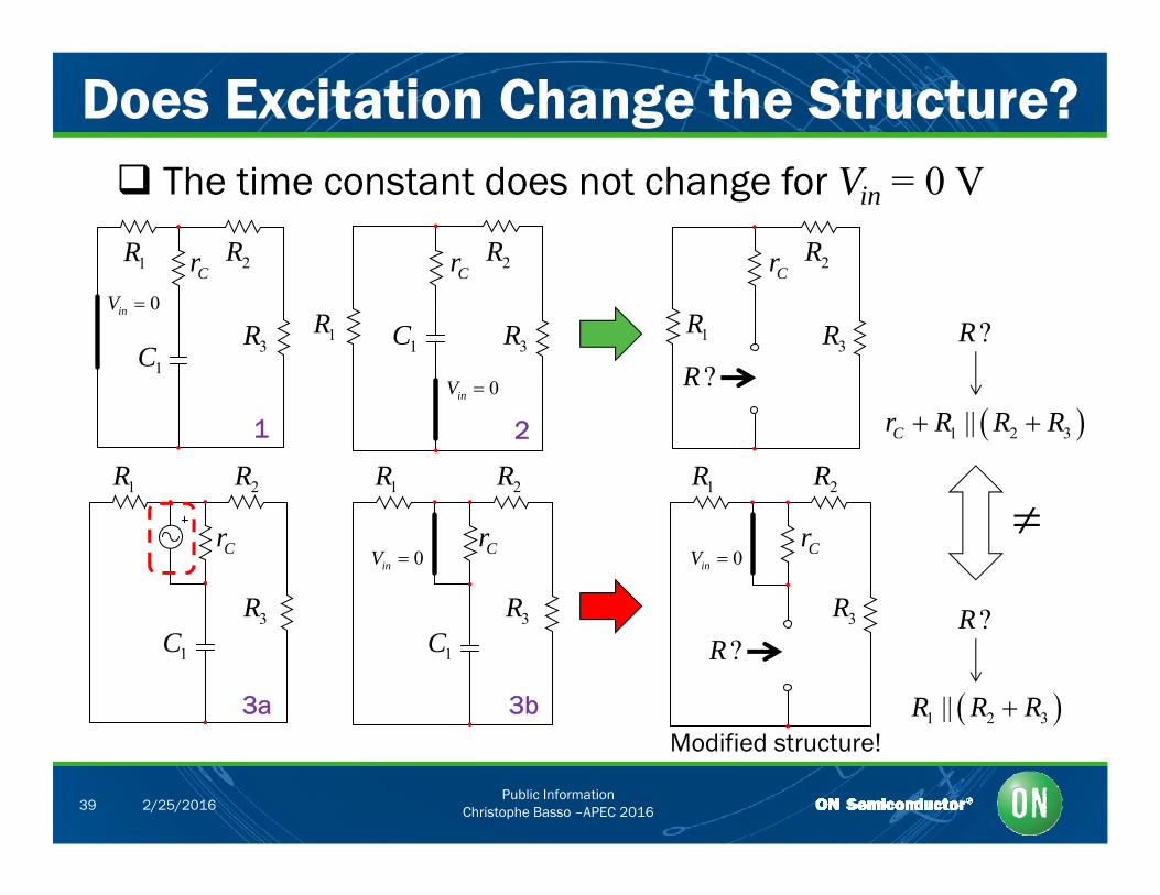
Does Excitation Change the Structure? The time constant does not change for Vin = 0 V
1RCr 2R
Cr 2RCr 2R
C
1C 3R 1R
C
1C 3R 1R
C
3R?R
?R0inV
0V
1R 2R 1R 2R 1R 2R
1 2 1 2 3||Cr R R R 0inV
Cr
3R
Cr
3R
Cr
3R ?R
0inV 0inV
1C3 3
1C3
?R
3a 3b 1 2 3||R R R
?R
Public InformationChristophe Basso –APEC 201639 2/25/2016
Modified structure!
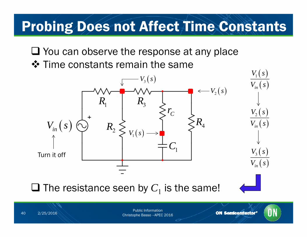
Probing Does not Affect Time Constants
You can observe the response at any place Time constants remain the same
V s
1R 3R 2V s
3V s
1
in
V sV s
1R
2R
3RCr
4R V s
inV s
2
in
V sV s
1C 1V s
3V sV s
Turn it off
The resistance seen by C1 is the same!
inV s
Public InformationChristophe Basso –APEC 201640 2/25/2016
1
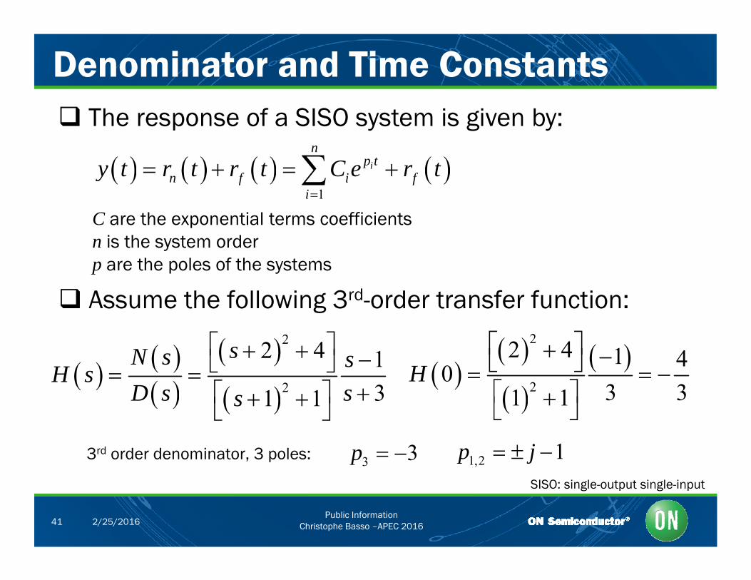
Denominator and Time Constants The response of a SISO system is given by:
i
np t
n f i fy t r t r t C e r t 1
n f i fi
y
C are the exponential terms coefficientsn is the system orderp are the poles of the systems
Assume the following 3rd-order transfer function:
2
2
2 4 131 1
sN s sH sD s ss
2
2
2 4 1 403 31 1
H
31 1D s ss 3 31 1
3rd order denominator, 3 poles: 1,2 1p j 3 3p
Public InformationChristophe Basso –APEC 201641 2/25/2016
SISO: single-output single-input
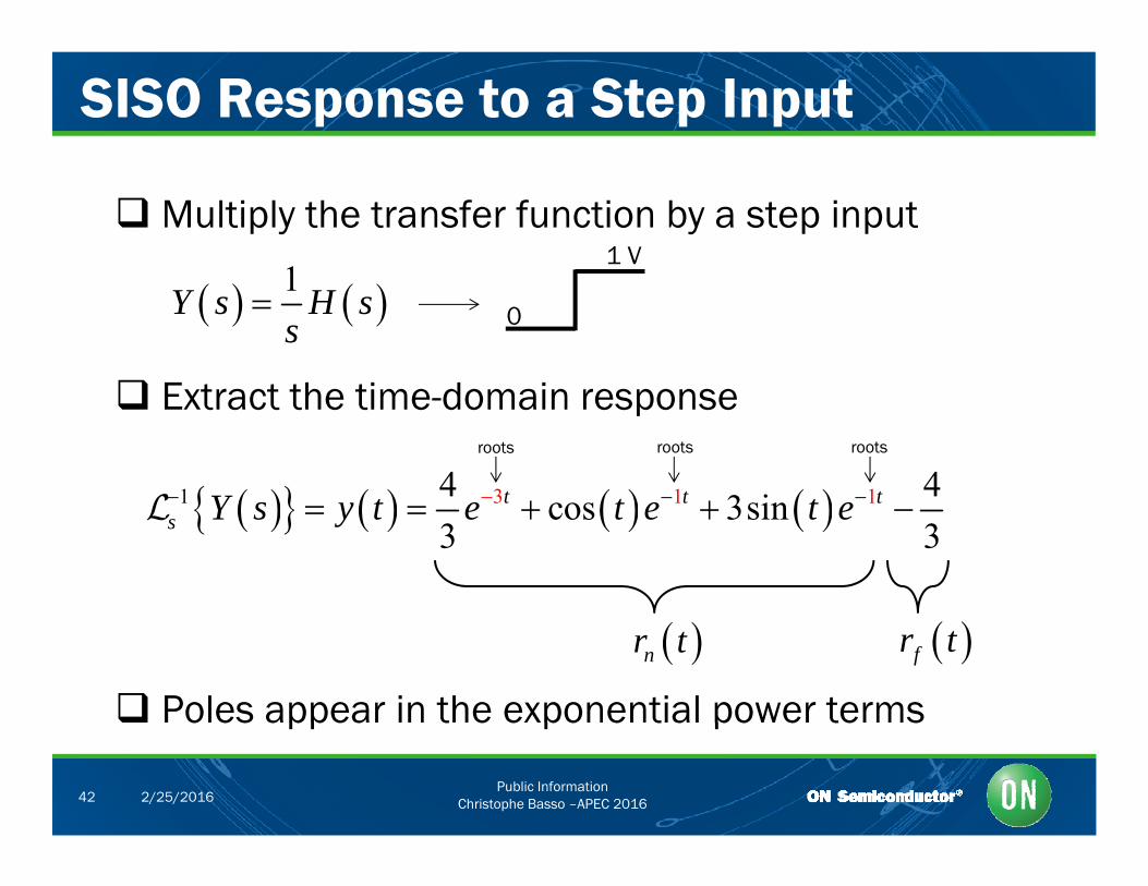
SISO Response to a Step Input
Multiply the transfer function by a step input
11 V
1Y s H ss
E t t th ti d i
0
3 1 11 4 43 it t tY t t t
Extract the time-domain responseroots roots roots
3 1 11 cos 3sin3 3
t t ts Y s y t e t e t e
nr t fr t
Poles appear in the exponential power terms
Public InformationChristophe Basso –APEC 201642 2/25/2016
o es appea t e e po e t a po e te s
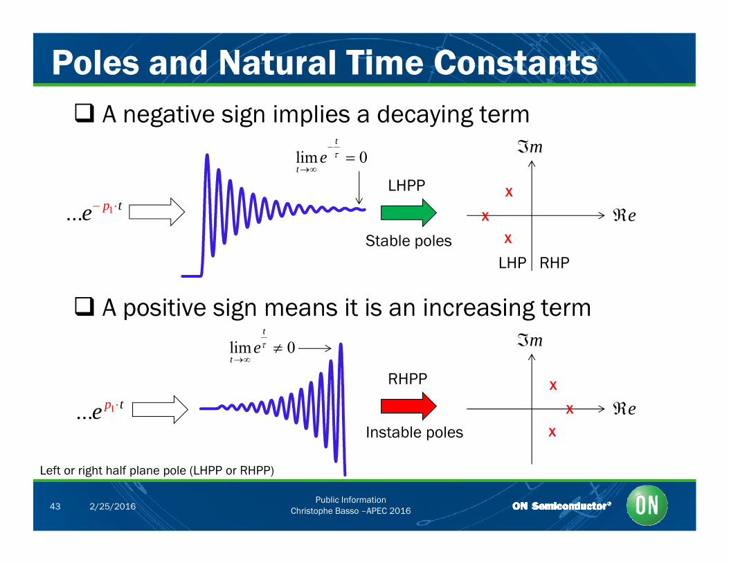
Poles and Natural Time Constants A negative sign implies a decaying term
mlim 0t
te
1... tpe LHPP
ex
x
xStable poles
A positive sign means it is an increasing term
Stab e po esLHP RHP
p g g
RHPP
m
x
lim 0t
te
1... tpe exx
xInstable poles
Public InformationChristophe Basso –APEC 201643 2/25/2016
Left or right half plane pole (LHPP or RHPP)
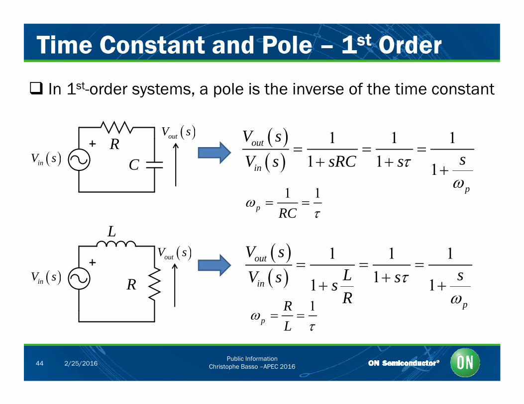
Time Constant and Pole – 1st Order
In 1st-order systems, a pole is the inverse of the time constant
C
1 1 11 1 1
out
in
V ssV s sRC s
outV sR
inV s
L
p1 1
p RC
L
1 1 11
outV sL sV s s
outV s
V s R 11 1in
p
L sV s ssR
1
pRL
inV s
Public InformationChristophe Basso –APEC 201644 2/25/2016
L
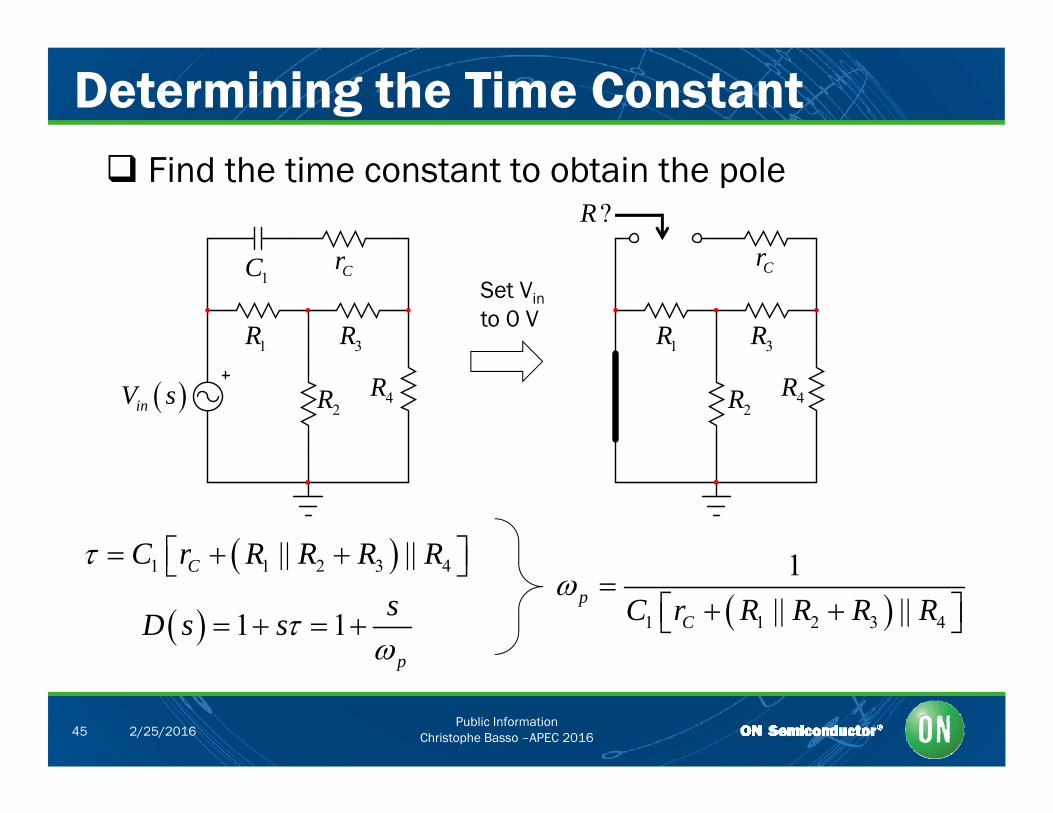
Determining the Time Constant Find the time constant to obtain the pole
?R
1R 3R
Cr1CSet Vinto 0 V
1R 3R
Cr
2R 4R inV s2R 4R
1 1 2 3 4|| ||CC r R R R R 1 1 1 2 3 4|| ||CC r R R R R
1 1p
sD s s
1 1 2 3 4
1|| ||p
CC r R R R R
Public InformationChristophe Basso –APEC 201645 2/25/2016
p
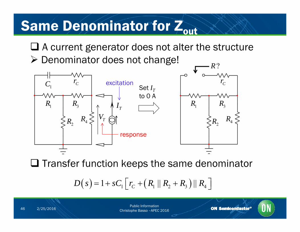
Same Denominator for Zout
A current generator does not alter the structure Denominator does not change!
?R
R R
Cr1C excitation
Set ITto 0 A
R R
Cr
1R 3R
2R 4RTI
TV1R 3R
2R 4R
response
T f f i k h d i
1 1 2 3 41 || ||CD s sC r R R R R
Transfer function keeps the same denominator
Public InformationChristophe Basso –APEC 201646 2/25/2016
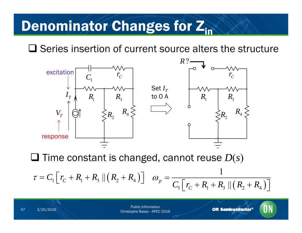
Denominator Changes for Zin
Series insertion of current source alters the structure
excitation
?R
1R 3R
Cr1C
TI
excitation
Set ITto 0 A 1R 3R
Cr
2R 4RTV
2R 4R
response
Time constant is changed, cannot reuse D(s) Time constant is changed, cannot reuse D(s)
1 1 3 2 4||CC r R R R R 1 1 3 2 4
1||p
CC r R R R R
Public InformationChristophe Basso –APEC 201647 2/25/2016
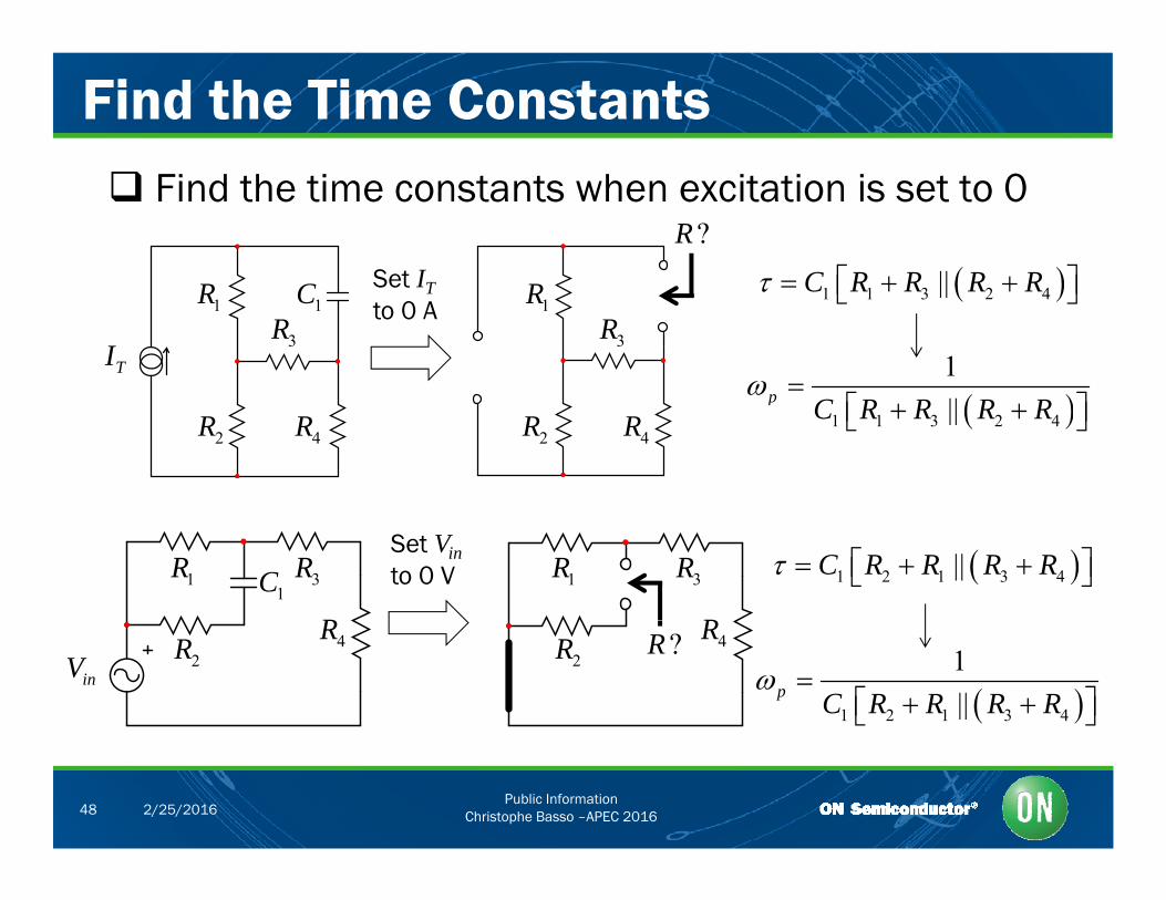
Find the Time Constants Find the time constants when excitation is set to 0
?RSet I ||C R R R R 1R
3R1C
TI
1R3R
Set ITto 0 A
1 1 3 2 4||C R R R R
1
2R 4R 2R 4R 1 1 3 2 4||p C R R R R
1R 3R1C
R
Set Vinto 0 V 1R 3R
R
1 2 1 3 4||C R R R R
2R 4RinV 2R 4R?R
1 2 1 3 4
1||p C R R R R
Public InformationChristophe Basso –APEC 201648 2/25/2016

Course Agenda
What is a Transfer Function? Why do We Need New Analytical Techniques? Why do We Need New Analytical Techniques? Time Constants and Poles Identifying the Zeros Identifying the Zeros The Null Double Injection 2nd-Order Networks 2 -Order Networks The PWM Switch Model A CCM Buck in Voltage Mode A CCM Buck in Voltage Mode A CCM Buck-Boost in Voltage Mode
Public InformationChristophe Basso –APEC 201649 2/25/2016
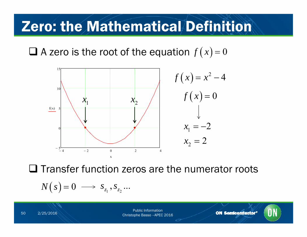
Zero: the Mathematical Definition
A zero is the root of the equation 0f x
15
2f10
2 4f x x
0f x 1x 2x
0
5f x( )
1 2x
1 2
4 2 0 2 45
x
2 2x
Transfer function zeros are the numerator roots
0N s 1 2, ...z zs s
Public InformationChristophe Basso –APEC 201650 2/25/2016
Nulling the Response
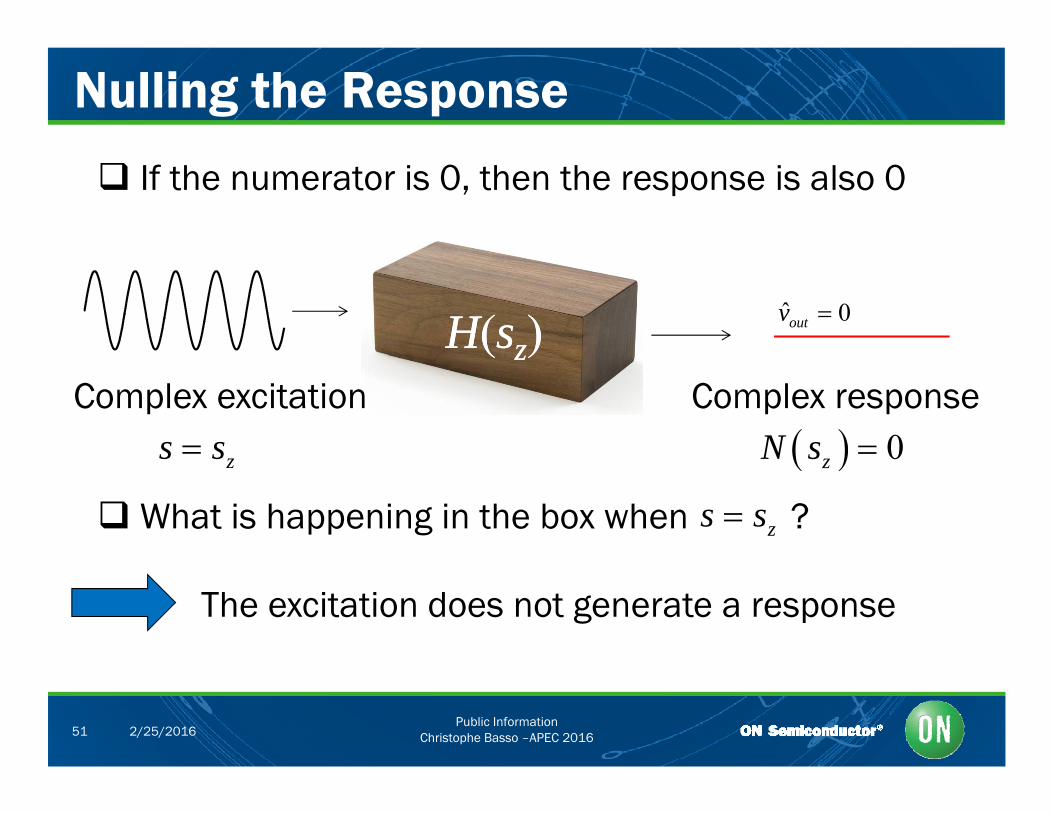
If the numerator is 0, then the response is also 0
HH((sszz))ˆ 0outv
Complex excitation
(( zz))
s s 0N s Complex response
zs s 0zN s
What is happening in the box when ? zs s
The excitation does not generate a response
Public InformationChristophe Basso –APEC 201651 2/25/2016
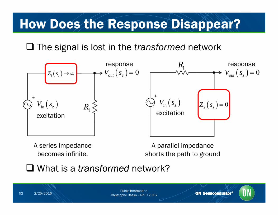
How Does the Response Disappear?
The signal is lost in the transformed network
1Rresponse response 1 zZ s
1Rp p 0out zV s 0out zV s
2 0zZ s in zV s in zV s1R
excitation excitation
A series impedance A parallel impedancepbecomes infinite.
p pshorts the path to ground
What is a transformedtransformed network?
Public InformationChristophe Basso –APEC 201652 2/25/2016
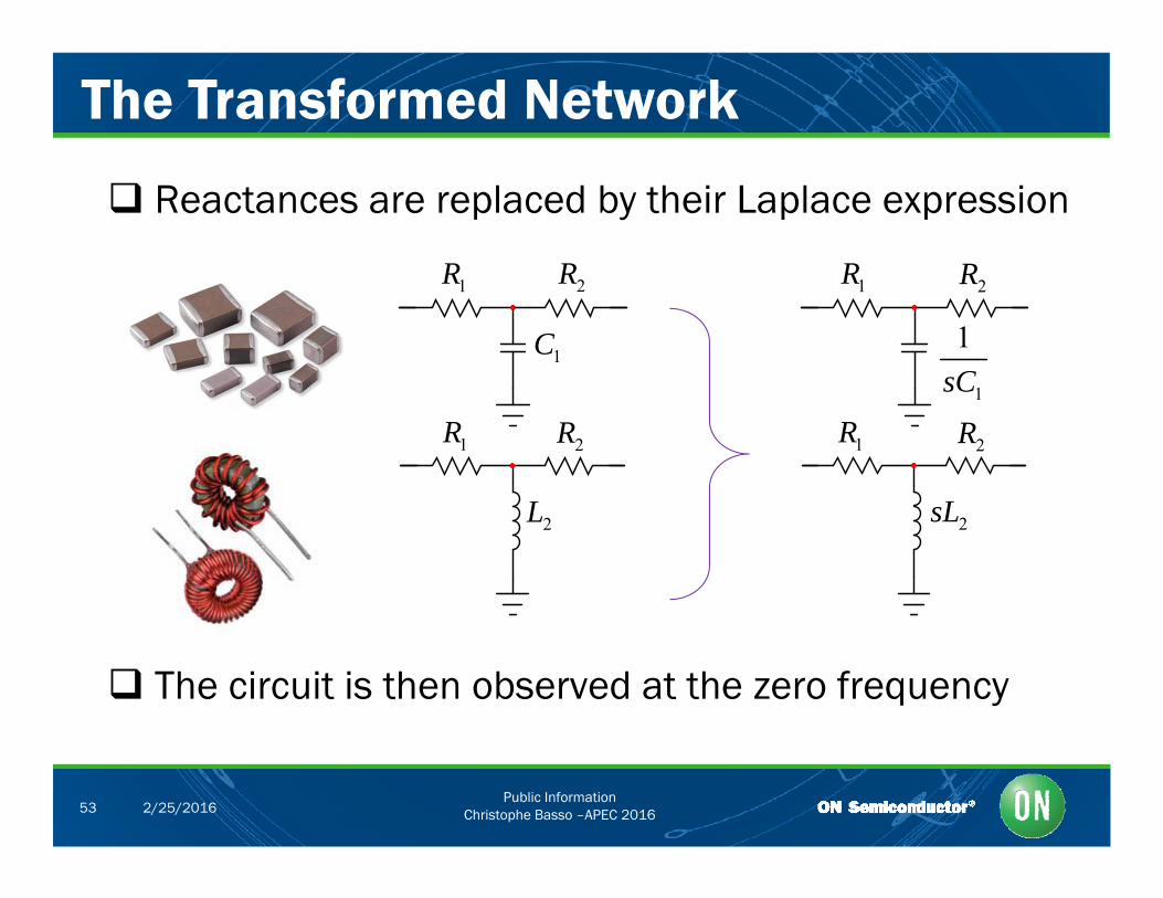
The Transformed Network
Reactances are replaced by their Laplace expression
R R R R1R 2R
1C
1R
1
1sC
2R
1
1R
L L
1R2R 2R
2L 2sL
The circuit is then observed at the zero frequency
Public InformationChristophe Basso –APEC 201653 2/25/2016
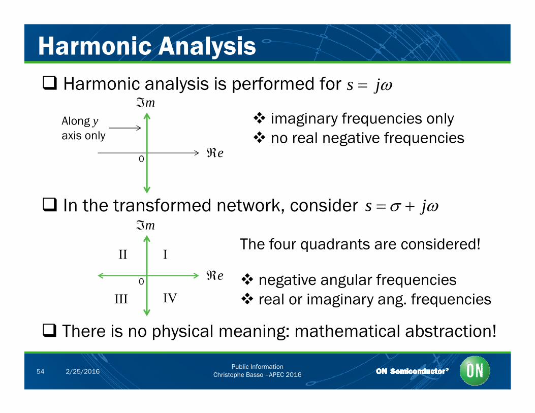
Harmonic Analysis Harmonic analysis is performed for s j
mAlong y imaginary frequencies only
e0
axis only no real negative frequencies
In the transformed network, consider s j m
e0
The four quadrants are considered!
negative angular frequencies
III
negative angular frequencies real or imaginary ang. frequencies
There is no physical meaning: mathematical abstraction!
IVIII
Public InformationChristophe Basso –APEC 201654 2/25/2016
There is no physical meaning: mathematical abstraction!
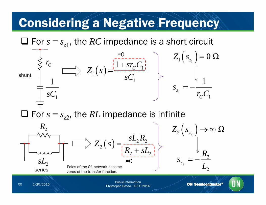
Considering a Negative Frequency For s = sz1, the RC impedance is a short circuit
Cr 1 sr C 11 0 ΩzZ s =0
Cr
1 1
11
1 Csr CZ s
sC
1
zs shunt
1sC 11
zCr C
For s = s 2 the RL impedance is infinite For s sz2, the RL impedance is infinite2R
2 2sL RZ
22 ΩzZ s
2sL
2 22
2 2
Z sR sL
2
2z
Rs
L =0
Poles of the RL network become
Public InformationChristophe Basso –APEC 201655 2/25/2016
2LseriesPoles of the RL network become zeros of the transfer function.
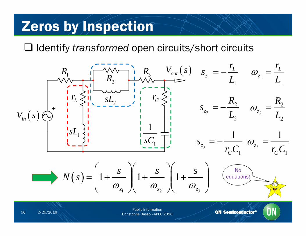
Zeros by Inspection Identify transformed open circuits/short circuits
1R 3R outV s Lrs Lr
Lr
1R2R
2sL
3R
Cr
out
2R
11
zsL
1
1z L
2R2
sL 1 inV s 2
2
2z
Rs
L
1
2
2
2z
RL
11sL1sC
31
1z
C
sr C
3
1
1z
Cr C
1 2 3
1 1 1z z z
s s sN s
Noequations!
Public InformationChristophe Basso –APEC 201656 2/25/2016
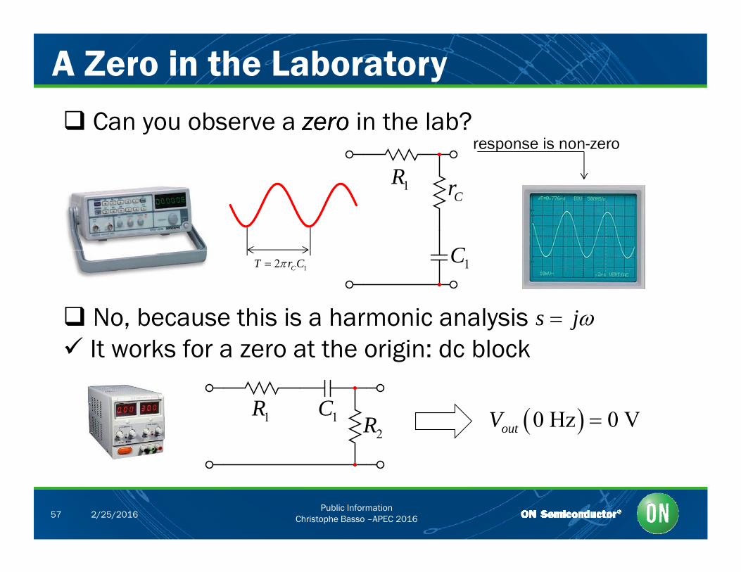
A Zero in the Laboratory Can you observe a zerozero in the lab?
Rresponse is non-zero
Cr
C
1R
1C
No because this is a harmonic analysis
12 CT r C
s j No, because this is a harmonic analysis It works for a zero at the origin: dc block
s j
1C1R2R 0 Hz 0 VoutV
Public InformationChristophe Basso –APEC 201657 2/25/2016
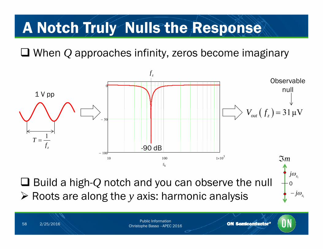
A Notch Truly Nulls the Response
fzf
When Q approaches infinity, zeros become imaginary
fk
0
1 V pp
Observablenull
5020 log H10 i 2 fk 10
1T
31µVout zV f
10 100 1 103100
fk
-90 dBz
Tf
m
j
1zj
Build a high-Q notch and you can observe the null Roots are along the y axis: harmonic analysis
1zj0
Public InformationChristophe Basso –APEC 201658 2/25/2016
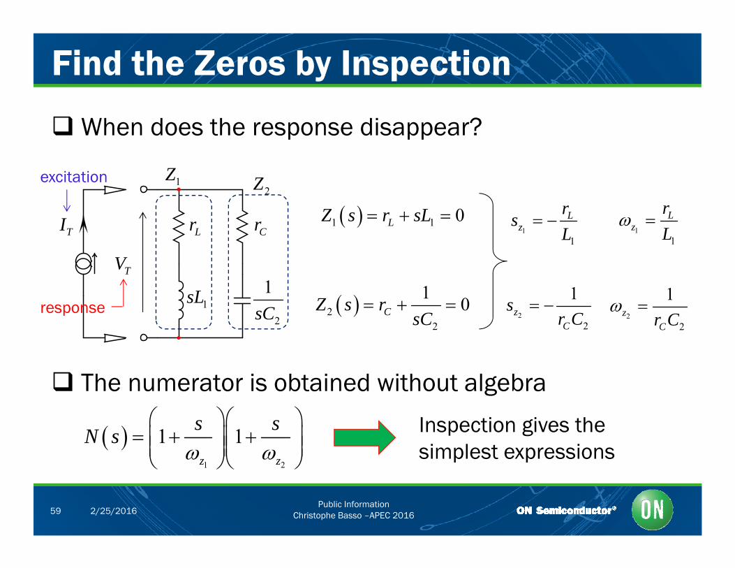
Find the Zeros by Inspection
When does the response disappear?
excitation Z
TI Lr Cr
excitation 1Z2Z
1 1 0LZ s r sL 1
1
Lz
rs
L
11
Lz
rL
TV
1sL2
1sCresponse 2
1 0CZ s rsC
2
1zs
r C
2
1z r C
2 2sC 2Cr C 2Cr C
The numerator is obtained without algebrag
1 2
1 1z z
s sN s
Inspection gives the simplest expressions
Public InformationChristophe Basso –APEC 201659 2/25/2016
1 2z z
Course Agenda
What is a Transfer Function? Why do We Need New Analytical Techniques? Why do We Need New Analytical Techniques? Time Constants and Poles Identifying the Zeros Identifying the Zeros The Null Double Injection 2nd-Order Networks 2 -Order Networks The PWM Switch Model A CCM Buck in Voltage Mode A CCM Buck in Voltage Mode A CCM Buck-Boost in Voltage Mode
Public InformationChristophe Basso –APEC 201660 2/25/2016
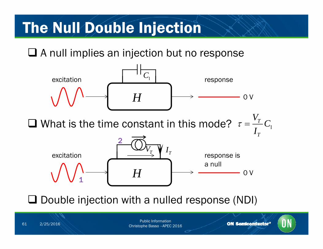
The Null Double Injection A null implies an injection but no response
1Cit ti
H
1C
0 V
excitation response
What is the time constant in this mode?2
1T
T
VC
I
H
TI
0 V
excitation response isa null
TV2
H 0 V1
Double injection with a nulled response (NDI)
Public InformationChristophe Basso –APEC 201661 2/25/2016
Double injection with a nulled response (NDI)
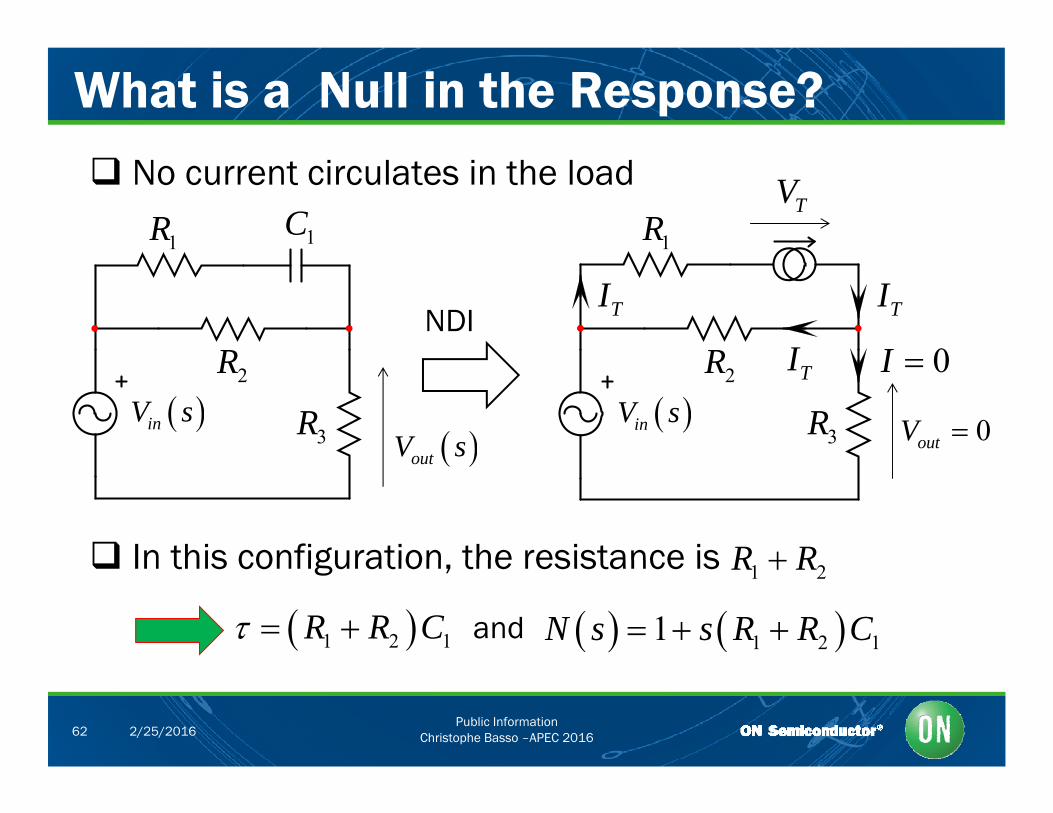
What is a Null in the Response? No current circulates in the load
1R 1C1R
TV
NDIR
TI
R 0IITI
2R
3R outV s inV s inV s
2R 0I TI
3R 0outV out
In this configuration the resistance is R R In this configuration, the resistance is 1 2R R
1 2 1R R C and 1 2 11N s s R R C
Public InformationChristophe Basso –APEC 201662 2/25/2016
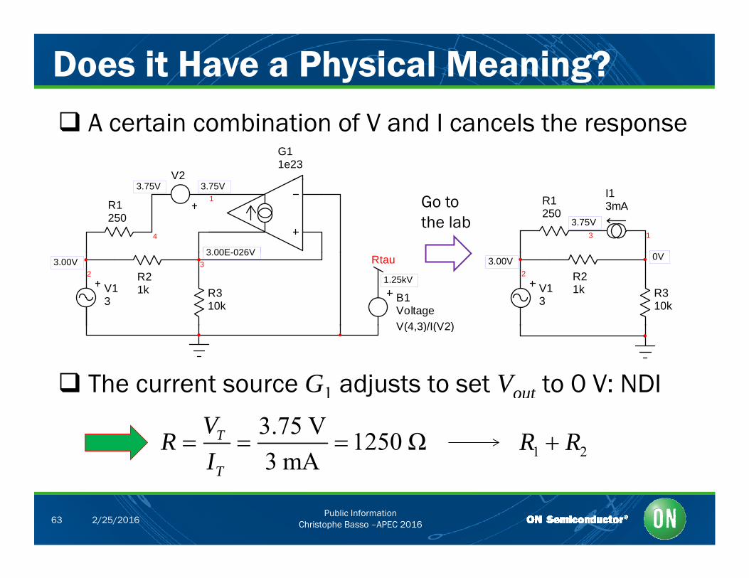
Does it Have a Physical Meaning? A certain combination of V and I cancels the response
G11e23
V2
R1250
4
1
3 00E-026V
3.75V 3.75V
1
R1250
3
I13mA
3.75V
Go tothe lab
23
V13
R310k
R21k
B1Voltage
Rtau
V(4 3)/I(V2)
3.00V3.00E-026V
1.25kV2
V13
R310k
R21k
3.00V 0V
V(4,3)/I(V2)
The current source G1 adjusts to set Vout to 0 V: NDI
3.75 V 1250 Ω3 mA
T
T
VR
I 1 2R R
Public InformationChristophe Basso –APEC 201663 2/25/2016
T
Inspection Would Work Here as Well What prevents the excitation from building a response?
1R 11 sC 1 zZ s
R 0out zV s
1
N sZ s
D s
2R
3R in zV s 0D s
out zV s
What is the denominator of Z1? Look at R driving C11
1 2R R R 1 1 21D s sC R R 1 1 2
1p C R R
Z1’s pole is H’s zero
Public InformationChristophe Basso –APEC 201664 2/25/2016
Z1 s pole is H s zero
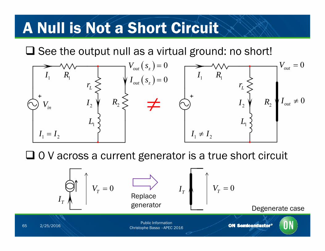
A Null is Not a Short Circuit See the output null as a virtual ground: no short!
1R 0out zV s
0I
0outV 1I 1I 1R
inV
1
Lr
2R
0out zI s
0outI
1
2I
1
2I
1
Lr
2R1L
1 2I I 1 2I I1L
0 V across a current generator is a true short circuit
TI0TV
Replacegenerator
0TV TI
Public InformationChristophe Basso –APEC 201665 2/25/2016
generator Degenerate case
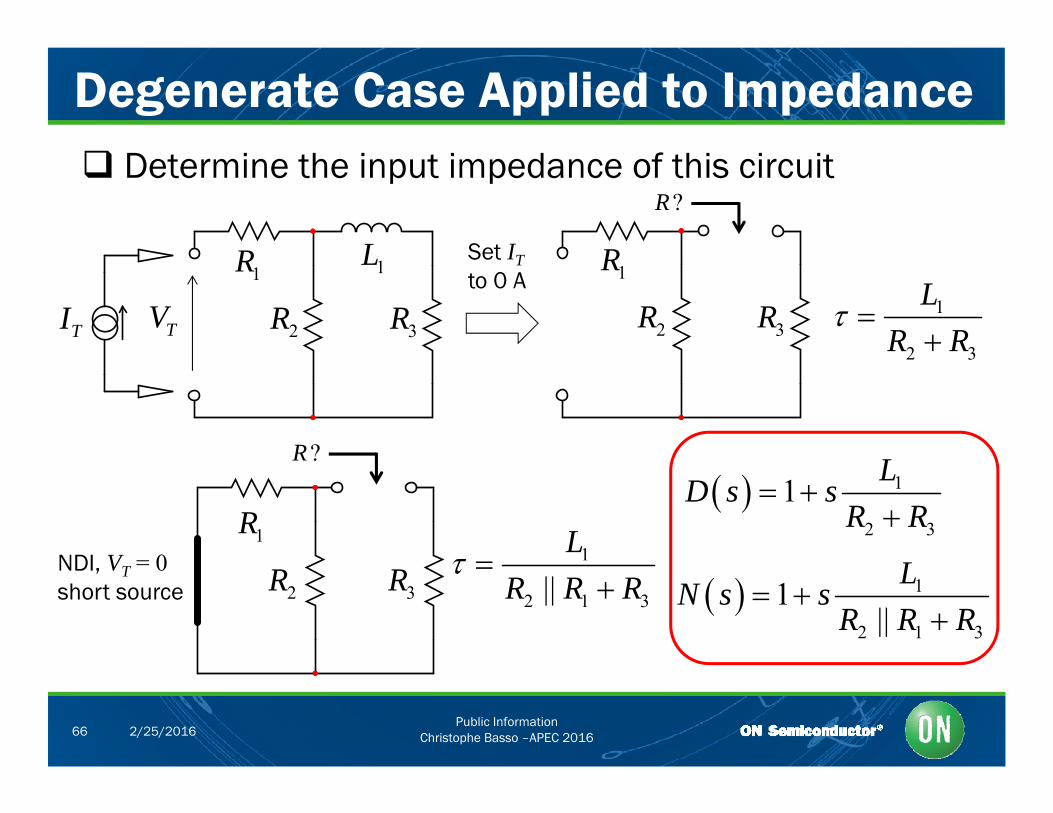
Degenerate Case Applied to Impedance Determine the input impedance of this circuit
R L Set I R
?R
1R
2R 3R
1L
TI TV
Set ITto 0 A 1R
2R 3R 1
2 3
LR R
2 3
?R
NDI V = 0
?R
1R1L
1
2 3
1L
D s sR R
NDI, VT = 0short source 2R 3R
2 1 3||R R R
1
2 1 3
1||
LN s s
R R R
Public InformationChristophe Basso –APEC 201666 2/25/2016
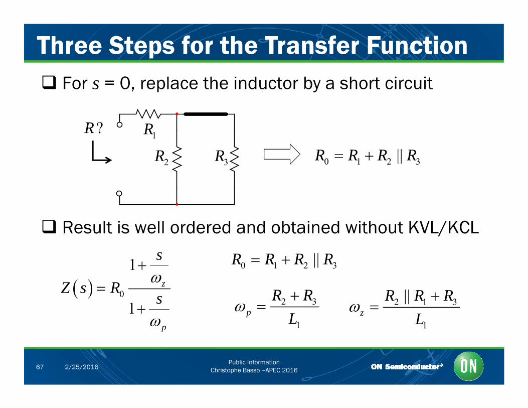
Three Steps for the Transfer Function For s = 0, replace the inductor by a short circuit
R?R 1R
2R 3R
?R
0 1 2 3||R R R R
Result is well ordered and obtained without KVL/KCL Result is well ordered and obtained without KVL/KCL
1 s
0 1 2 3||R R R R
0
1
z
p
Z s Rs
2 3
1p
R RL
2 1 3
1
||z
R R RL
Public InformationChristophe Basso –APEC 201667 2/25/2016
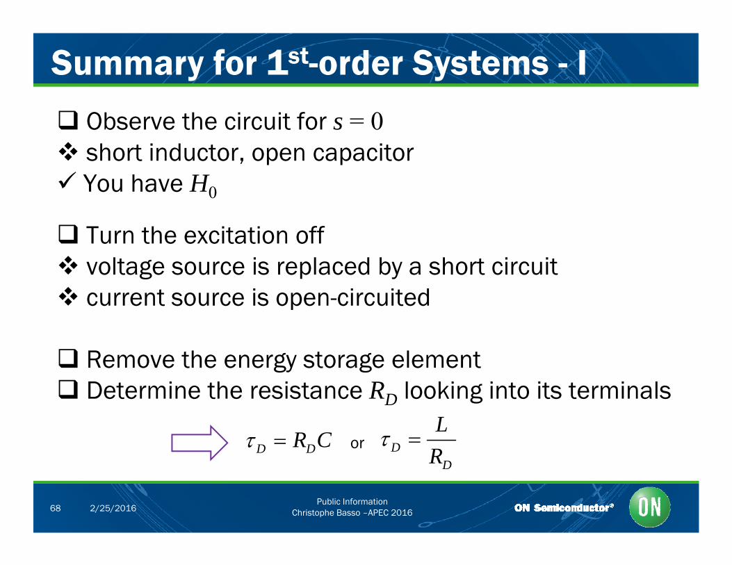
Summary for 1st-order Systems - I
Observe the circuit for s = 0 short inductor, open capacitor Y h H You have H0
Turn the excitation off voltage source is replaced by a short circuit current source is open-circuited
Remove the energy storage element Determine the resistance R looking into its terminals Determine the resistance RD looking into its terminals
D DR C or DD
LR
Public InformationChristophe Basso –APEC 201668 2/25/2016
DR
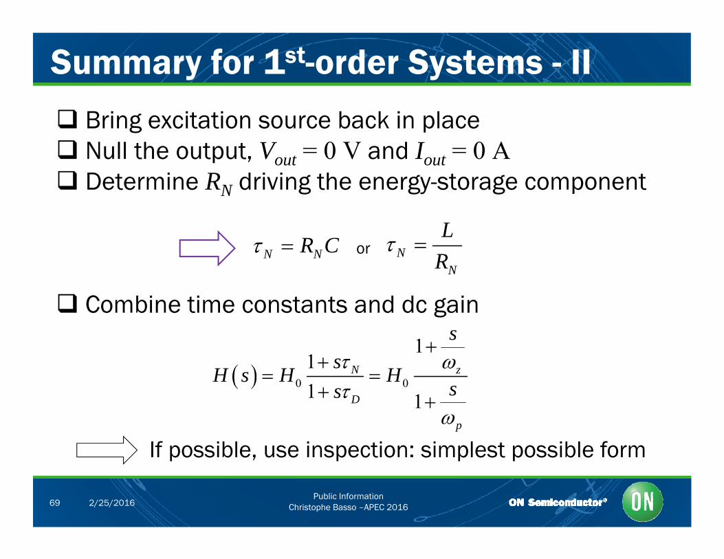
Summary for 1st-order Systems - II
Bring excitation source back in place Null the output, Vout = 0 V and Iout = 0 A D t i R d i i th t t Determine RN driving the energy-storage component
R C L
Combine time constants and dc gain
N NR C or NNR
g
0 0
111
N z
ss
H s H H
0 01 1D
p
ss
If possible, use inspection: simplest possible form
Public InformationChristophe Basso –APEC 201669 2/25/2016
If possible, use inspection: simplest possible form
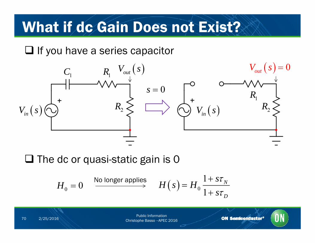
What if dc Gain Does not Exist? If you have a series capacitor
1C 1R outV s 0outV s 1 1
R
0s 1R
R 2R inV s 2R inV s
The dc or quasi-static gain is 0
0 0H 011
N
D
sH s H
s
No longer applies
Public InformationChristophe Basso –APEC 201670 2/25/2016
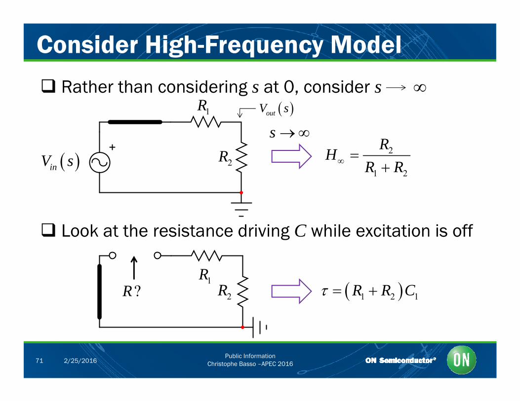
Consider High-Frequency Model
Rather than considering s at 0, consider s 1R outV s
2R inV s
s 2
1 2
RH
R R 1 2
L k t th i t d i i C hil it ti i ff Look at the resistance driving C while excitation is off
R1R2R?R 1 2 1R R C
Public InformationChristophe Basso –APEC 201671 2/25/2016
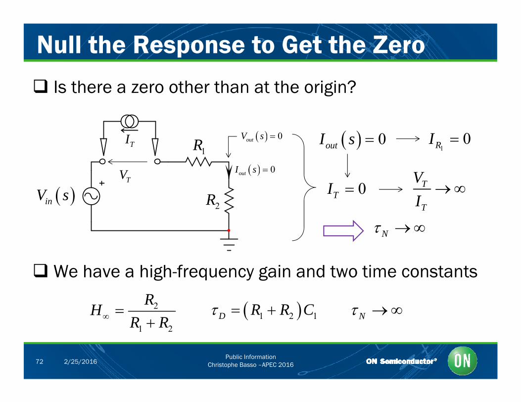
Null the Response to Get the Zero
Is there a zero other than at the origin?
1R 0outV s
0outI s
TI
V
0outI s 1
0RI
V2R inV s
TV
0TI T
T
VI
N
We have a high-frequency gain and two time constants We have a high frequency gain and two time constants
2
1 2
RH
R R
1 2 1D R R C N
Public InformationChristophe Basso –APEC 201672 2/25/2016
1 2
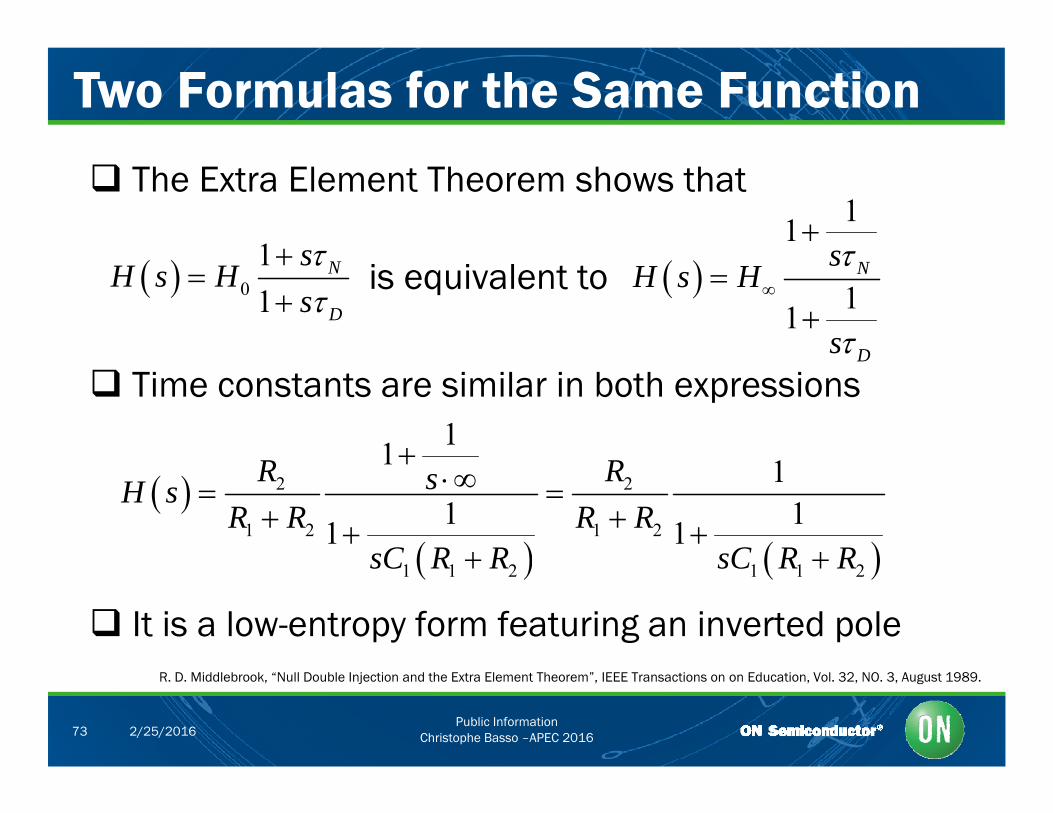
Two Formulas for the Same Function
11s
The Extra Element Theorem shows that
1 s 11
N
D
sH s H
s
011
N
D
sH s H
s
is equivalent to
D
Time constants are similar in both expressions11
2 2
1 2 1 2
1 11 11 1
R RsH sR R R R
sC R R sC R R
1 1 2 1 1 2sC R R sC R R
It is a low-entropy form featuring an inverted pole
Public InformationChristophe Basso –APEC 201673 2/25/2016
R. D. Middlebrook, “Null Double Injection and the Extra Element Theorem”, IEEE Transactions on on Education, Vol. 32, NO. 3, August 1989.
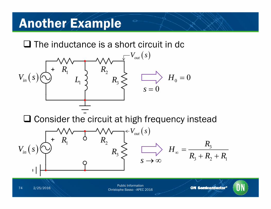
Another Example The inductance is a short circuit in dc
outV s
1R 2R3R1L inV s
0s 0 0H
0s
Consider the circuit at high frequency instead Consider the circuit at high frequency instead
1R 2R R outV s
1 2
3R inV ss
3
3 2 1
RH
R R R
Public InformationChristophe Basso –APEC 201674 2/25/2016
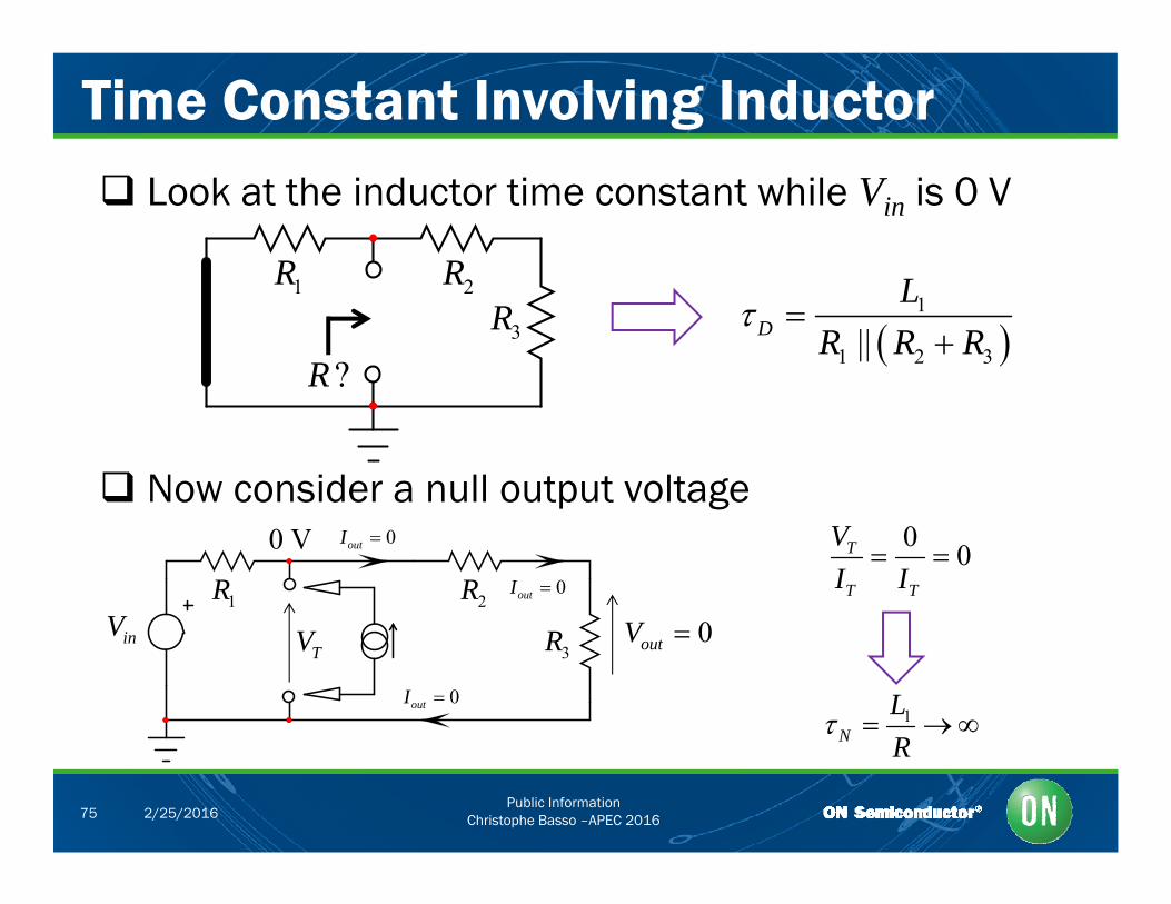
Time Constant Involving Inductor Look at the inductor time constant while Vin is 0 V
1R 2R L1R 2R3R
?R
1
1 2 3||DL
R R R
Now consider a null output voltageg
1R 2R 0outI
0outI
0VV
0 V 0 0T
T T
VI I
3R
0outI
0outV TVinV
1N
LR
Public InformationChristophe Basso –APEC 201675 2/25/2016
N R
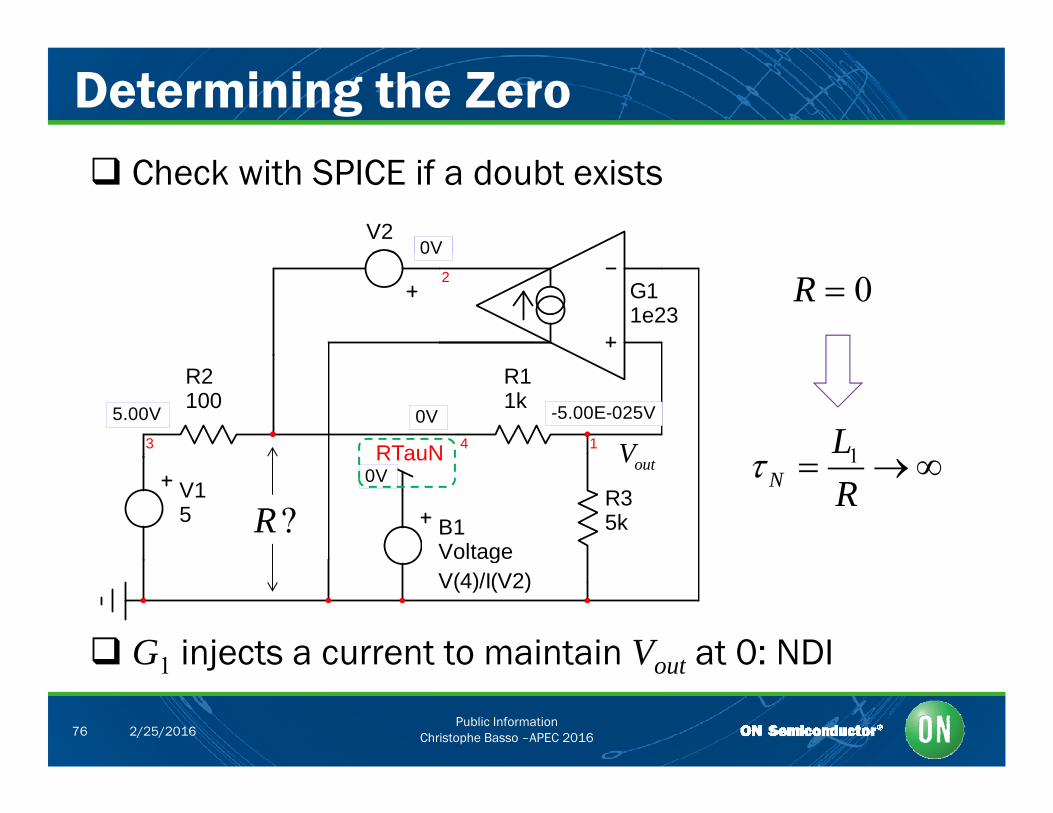
Determining the Zero
V20V
Check with SPICE if a doubt exists
2G11e23
0V
0R
4 1
R11k
3
R2100
RTauN
0V -5.00E-025V5.00V
1LVR35k
V15 B1
Voltage
RTauN0V
1N R
?R
outV
gV(4)/I(V2)
G1 injects a current to maintain Vout at 0: NDI
Public InformationChristophe Basso –APEC 201676 2/25/2016
G1 injects a current to maintain Vout at 0: NDI
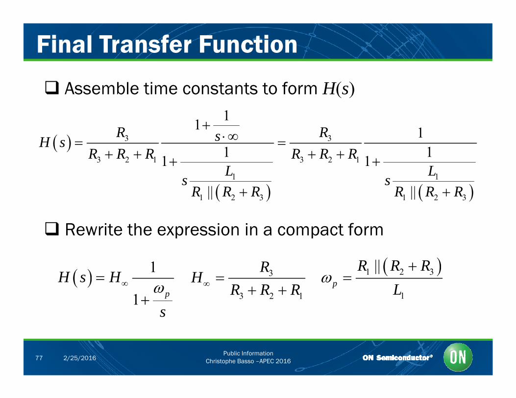
Final Transfer Function
Assemble time constants to form H(s)11
3 3
3 2 1 3 2 1
1 1
1 11 11 1
R RsH sR R R R R R
L L
1 1
1 2 3 1 2 3|| ||L Ls s
R R R R R R
R it th i i t f Rewrite the expression in a compact form
1H H 1 2 3||R R R3R
H 1 p
H s H
s
1 2 3
1p L
3
3 2 1
HR R R
Public InformationChristophe Basso –APEC 201677 2/25/2016
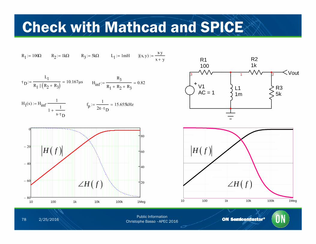
Check with Mathcad and SPICE
1 2
R21k
3
R1100
Vout
R1 100 R2 1k R3 5k L1 1mH || x y( )x y
x y
L
R35k
V1AC = 1
L11m
DL1
R1 || R2 R3 10.167s HinfR3
R1 R2 R30.82
H1 s( ) Hinf1
1 fp
12
15.655kHz
0
80
11
s D
p 2 D
40
20
40
60 H f H f
80
60 20 H f H f
Public InformationChristophe Basso –APEC 201678 2/25/2016
10 100 1k 10k 100k 1Meg 10 100 1k 10k 100k 1Meg
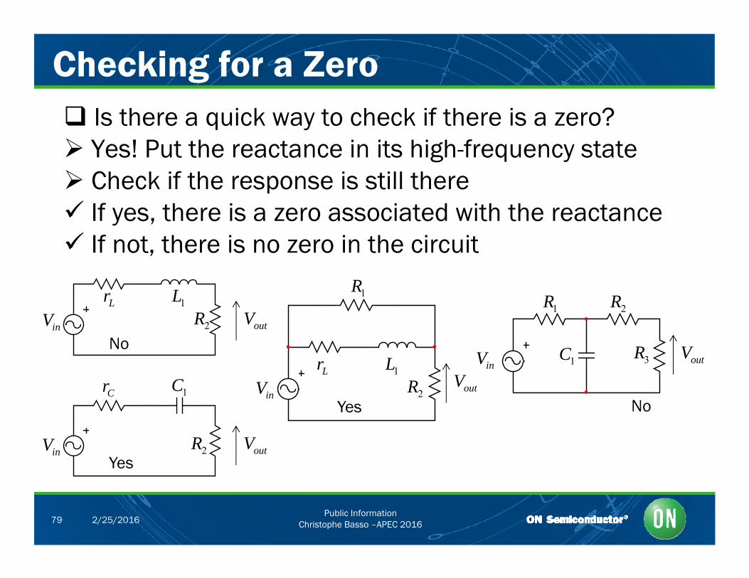
Checking for a Zero Is there a quick way to check if there is a zero? Yes! Put the reactance in its high-frequency state Check if the response is still there Check if the response is still there If yes, there is a zero associated with the reactance If not, there is no zero in the circuitot, t e e s o e o t e c cu t
Lr 1LiV outV2R
1R1R 2R
inV out2
Cr 1CLr 1L
inV outV2R
inV 3R1CNooutV
inV outV2R
inNo
Yes
Yes
Public InformationChristophe Basso –APEC 201679 2/25/2016

Course Agenda
What is a Transfer Function? Why do We Need New Analytical Techniques? Why do We Need New Analytical Techniques? Time Constants and Poles Identifying the Zeros Identifying the Zeros The Null Double Injection 2nd-Order Networks 2 -Order Networks The PWM Switch Model A CCM Buck in Voltage Mode A CCM Buck in Voltage Mode A CCM Buck-Boost in Voltage Mode
Public InformationChristophe Basso –APEC 201680 2/25/2016
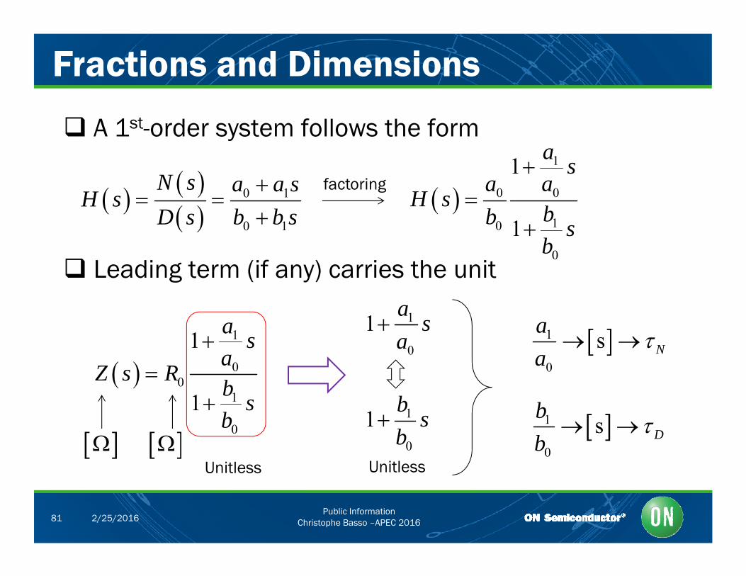
Fractions and Dimensions
A 1st-order system follows the form
N11 a s
f t i
0 1
0 1
N s a a sH s
D s b b s
0 0
10
0
1
a aH s
bb sb
factoring
Leading term (if any) carries the unit0b
a 11a
s a
1
00
1
1
1
a sa
Z s Rb
0
1 sa
b
1
0
s Naa
1
0
1 sb
Unitless
1
0
1b
sb
Unitless
1
0
s Dbb
Public InformationChristophe Basso –APEC 201681 2/25/2016
Unitless Unitless
2nd-Order System
A 2nd-order system follows the form
2
2
0 1 22
0 1 2
s sH s
s s
21 2
0 21 2
11
a s a sH s H
b s b s
Factoring 0Unitless
Factoring 0
The second fraction is unitless
Carries the unit
11 1 2
0
s N Na
2 1 222 1 2 2 1
0
s orN N N Na
sum product
11 1 2
0
s D Db
1 2
2 1 222 1 2 2 1
0
s orD D D Db
Public InformationChristophe Basso –APEC 201682 2/25/2016
reactance 1 reactance 2
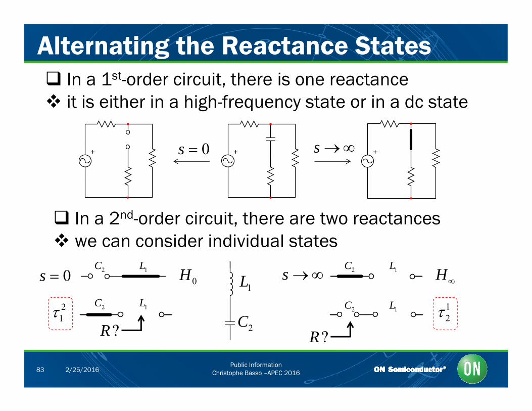
Alternating the Reactance States In a 1st order circuit there is one reactance In a 1st-order circuit, there is one reactance it is either in a high-frequency state or in a dc state
0s s
In a 2nd-order circuit, there are two reactances we can consider individual states
0s L s 0H H1L2C 1L2C
1L
2C
0
?R ?R
21
12
1L2C1L2C
Public InformationChristophe Basso –APEC 201683 2/25/2016
?R ?R
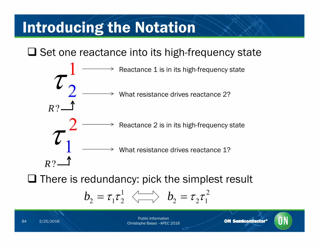
Introducing the Notation Set one reactance into its high-frequency state
1 Reactance 1 is in its high-frequency state
2?R
What resistance drives reactance 2?
?R
2 Reactance 2 is in its high-frequency state
1?R
What resistance drives reactance 1?
There is redundancy: pick the simplest result1
2 1 2b 22 2 1b
Public InformationChristophe Basso –APEC 201684 2/25/2016
2 1 2 2 2 1
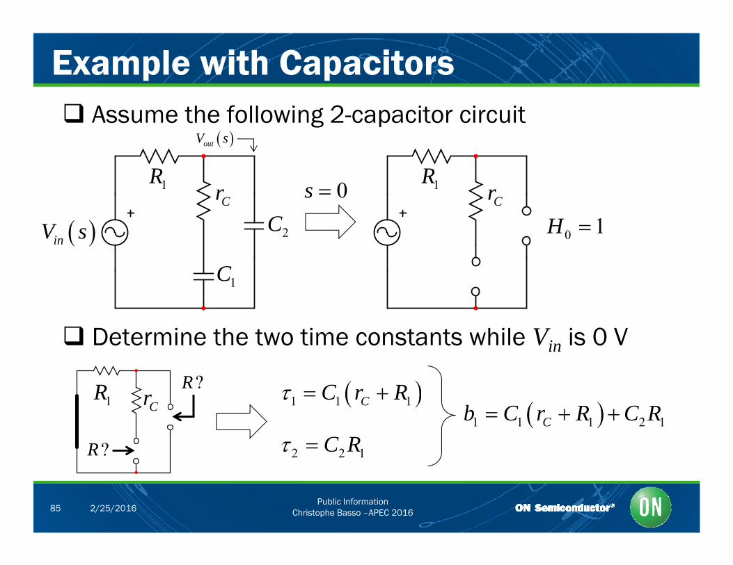
Example with Capacitors Assume the following 2-capacitor circuit
R
outV s
R1RCr
2C inV s
0s 1RCr
0 1H
1C
Determine the two time constants while Vin is 0 V
R ?R C R 1RCr
?R
1 1 1CC r R
2 2 1C R 1 1 1 2 1Cb C r R C R
Public InformationChristophe Basso –APEC 201685 2/25/2016
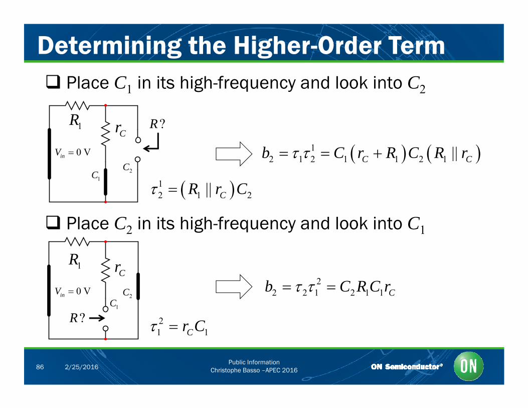
Determining the Higher-Order Term Place C1 in its high-frequency and look into C2
1R r ?R1Cr ?R
12 1 2 1 1 2 1 ||C Cb C r R C R r 0 VinV
1C 2C
12 1 2|| CR r C
Place C2 in its high-frequency and look into C1
1
2 g q y 1
1RCr
2b C R C
?R 21 1Cr C
22 2 1 2 1 1 Cb C R C r 0 VinV
1C2C
Public InformationChristophe Basso –APEC 201686 2/25/2016
1 1C
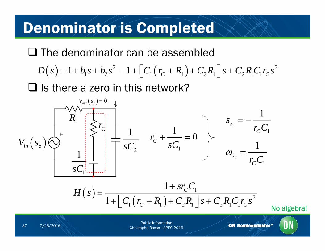
Denominator is Completed The denominator can be assembled
2 21 2 1 1 2 1 2 1 11 1 C CD s b s b s C r R C R s C R C r s
Is there a zero in this network? 0out zV s
1RCr 1
V s1 0Cr C
1
1
1z
C
sr C
1
1sC
2sC in zV s1
C sC1
1
1z
Cr C
1
12
1 1 2 1 2 1 1
11
C
C C
sr CH s
C r R C R s C R C r s
Public InformationChristophe Basso –APEC 201687 2/25/2016
1 1 2 1 2 1 1C C No algebra!

You Can Rework the Denominator Considering a low quality factor Q (roots are spread)
2
2 21 1 1 1bs sD s b s b s b s s
2
1 2 10 0 1
1 1 1 1D s b s b s b s sQ b
Low-frequency High-frequency
1 sr C
1
2 1 11 1 2 1
1 1 2 1
1
1 1
C
CC
C
sr CH s
C R C rs C r R C R sC r R C R
1 1 2 1CC C
1
z
s
H s
1z r C
2
1 1 2 1Cp
C r R C RC R C r
1 2
1 1p p
H ss s
1
1
1 1 2 1
1C
pC
r C
R C C r C
2 1 1 CC R C r
Public InformationChristophe Basso –APEC 201688 2/25/2016
1 1 2 1CR C C r C
Check with Mathcad It is easy to check results versus a raw expression
R1 1k rC 100 C1 10nF C2 5nF || x y( )x y
x y Z1 s( ) rC
1s C1
||1
s C2
H0 1 1 C1 rC R1 11s 2 C2 R1 5s a1 1 2 16s
H2 s( )Z1 s( )
R1 Z1 s( )
12 C2 R1 || rC 0.455s 21 C1 rC a2 2 21 5s 2
N1 s( ) 1 s rC C1 D1 s( ) 1 a1 s a2 s2 H1 s( ) H0
N1 s( )
0 0
180
1( ) C 1 1( ) 1 2 1( ) 0 D1 s( )
z1
rC C1
1
40
20
100
5020 log H1 i 2 fk 10
20 log H2 i 2 fk 10
20 log H3 i 2 fk 10
arg H1 i 2 fk 180
arg H2 i 2 fk 180
arg H3 i 2 fk 180
p11a1
p2a1a
10 100 1 103 1 104 1 105 1 106 1 10780
60
150
a g 3 k
p a2
H3 s( )
1sz
1s
1s
Public InformationChristophe Basso –APEC 201689 2/25/2016
fkp1 p2
2nd-Order Example What is the buck converter output impedance?
outZ s1L
DinV
1
2C loadR
Voltage mode
Consider parasitic elements for L and CVoltage-mode
outout
V sZ s
I s
response
excitation
outI s2C1L
loadR outV s outI s excitation
Lr Cr
load out
Public InformationChristophe Basso –APEC 201690 2/25/2016
Buck Output Impedance
V
Let's find the term R0 in dc: open caps, short inductors
0 ||TL load
T
VR r RI
Lr loadRTITV
0sL r 1 1 0Lr s
The zeros cancel the responseLr
0?out zV s 1 0LsL r
1 0CrC
1 0LL
r sr
21 0Csr C
1sL2
1sC
loadR
out zI s2
2
1z
Cr C
11
z L
2CsC
Lr Cr
load 2C
121 1 C
L
LN s s sr Cr
Public InformationChristophe Basso –APEC 201691 2/25/2016
L
Low-Frequency Time Constants All elements are in their dc state Look at R driving L then R driving C
?R1 2
?R
r r
loadR
r r
loadR1L 2C 1L 2C
Lr Cr
R r R
Lr Cr
||R r R r L loadR r R ||L load CR r R r
11 2 ||L load C
L l d
Lb C r R rr R
Public InformationChristophe Basso –APEC 201692 2/25/2016
L loadr R
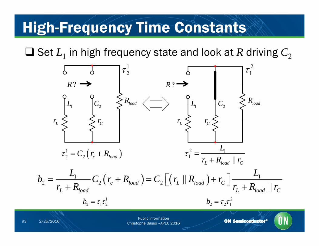
High-Frequency Time Constants
12
21
Set L1 in high frequency state and look at R driving C2
loadR loadR
?R ?R
1L 2C 1L 2C
Lr Cr Lr Cr
1 2 1 2
12 2 c loadC r R 2 1
1 ||L load C
Lr R r
L L 1 12 2 2 ||
||c load L load CL load L load C
L Lb C r R C r R rr R r R r
1b 2b
Public InformationChristophe Basso –APEC 201693 2/25/2016
2 1 2b 2 2 1b
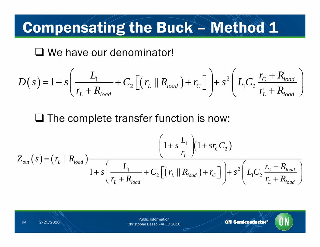
Compensating the Buck – Method 1 We have our denominator!
2 r RL 21
2 1 21 || C loadL load C
L load L load
r RLD s s C r R r s L Cr R r R
The complete transfer function is now:
L
12
21
1 1||
1 ||
CL
out L loadC load
Ls sr Cr
Z s r Rr RL C R L C
212 1 21 || C load
L load CL load L load
s C r R r s L Cr R r R
Public InformationChristophe Basso –APEC 201694 2/25/2016
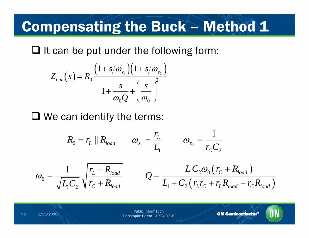
Compensating the Buck – Method 1 It can be put under the following form:
1 21 1z zs s
Z R
1 2
0 2
0 0
1outZ s R
s sQ
We can identify the terms:
r 10 ||L loadR r R
11
Lz
rL
2
2
1z
Cr C
0
1 2
1 L load
C load
r Rr RL C
1 2 0
1 2
C load
L C L load C load
L C r RQ
L C r r r R r R
Public InformationChristophe Basso –APEC 201695 2/25/2016
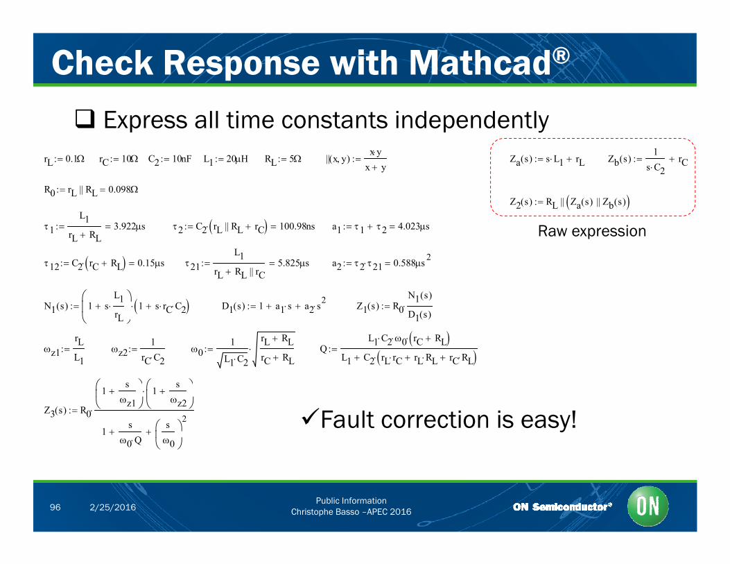
Check Response with Mathcad®
rL 0.1 rC 10 C2 10nF L1 20H RL 5 || x y( )x y
x y Za s( ) s L1 rL Zb s( )
1s C2
rC
Express all time constants independently
R0 rL || RL 0.098Z2 s( ) RL || Za s( ) || Zb s( )
1L1
rL RL3.922s 2 C2 rL || RL rC 100.98ns a1 1 2 4.023s Raw expression
12 C2 rC RL 0.15s 21L1
rL RL || rC5.825s a2 2 21 0.588s 2
N1 s( ) 1 sL1rL
1 s rC C2 D1 s( ) 1 a1 s a2 s2 Z1 s( ) R0
N1 s( )
D1 s( )
L 1( )
z1rLL1
z21
rC C2 0
1
L1 C2
rL RL
rC RL Q
L1 C2 0 rC RL
L1 C2 rL rC rL RL rC RL
1s 1
s
Z3 s( ) R0
1z1
1z2
1s
0 Q
s0
2
Fault correction is easy!
Public InformationChristophe Basso –APEC 201696 2/25/2016
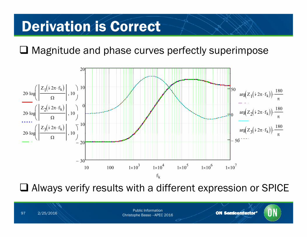
Derivation is Correct
20
Magnitude and phase curves perfectly superimpose
10 5020 log
Z1 i 2 fk
10
arg Z1 i 2 fk 180
10
0
020 logZ2 i 2 fk
10
20 logZ3 i 2 fk
10
arg Z2 i 2 fk 180
arg Z3 i 2 fk 180
30
20 50
20 log
10
10 100 1 103 1 104 1 105 1 106 1 107
fk
Always verify results with a different expression or SPICE
Public InformationChristophe Basso –APEC 201697 2/25/2016
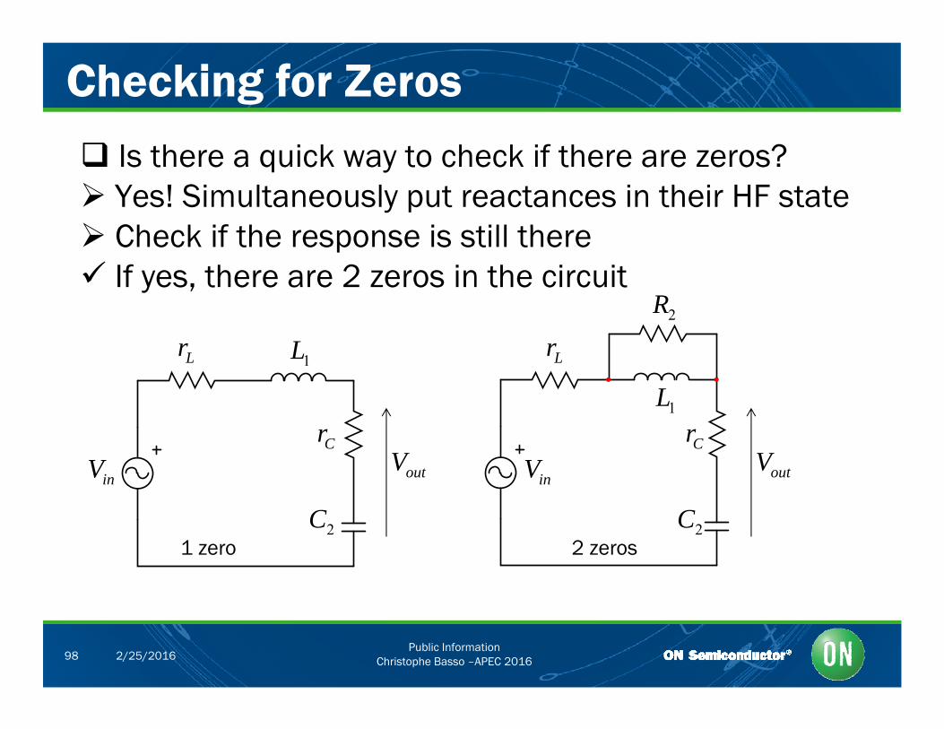
Checking for Zeros Is there a quick way to check if there are zeros? Yes! Simultaneously put reactances in their HF state Ch k if th i till th Check if the response is still there If yes, there are 2 zeros in the circuit
2R
Lr 1L Lr
1L
2
inV outVinV outV
Cr1
Cr
2C 2C1 zero 2 zeros
Public InformationChristophe Basso –APEC 201698 2/25/2016

Course Agenda
What is a Transfer Function? Why do We Need New Analytical Techniques? Why do We Need New Analytical Techniques? Time Constants and Poles Identifying the Zeros Identifying the Zeros The Null Double Injection 2nd-Order Networks 2 -Order Networks The PWM Switch Model A CCM Buck in Voltage Mode A CCM Buck in Voltage Mode A CCM Buck-Boost in Voltage Mode
Public InformationChristophe Basso –APEC 201699 2/25/2016
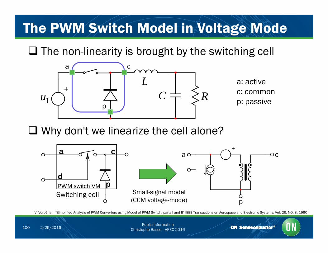
The PWM Switch Model in Voltage Mode
The non-linearity is brought by the switching cell
La c
L1u C R
p
a: activec: commonp: passive
Why don't we linearize the cell alone?
d
a c a c. .
dPWM switch VM p
pSwitching cell Small-signal model
(CCM voltage-mode)
Public InformationChristophe Basso –APEC 2016100 2/25/2016
V. Vorpérian, "Simplified Analysis of PWM Converters using Model of PWM Switch, parts I and II” IEEE Transactions on Aerospace and Electronic Systems, Vol. 26, NO. 3, 1990
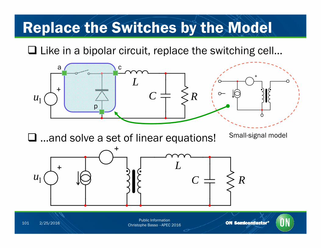
Replace the Switches by the Model Like in a bipolar circuit, replace the switching cell…
a c
L1u C R
p
..
p
and solve a set of linear equations! Small-signal model …and solve a set of linear equations!
. . L. .1u C R
Public InformationChristophe Basso –APEC 2016101 2/25/2016
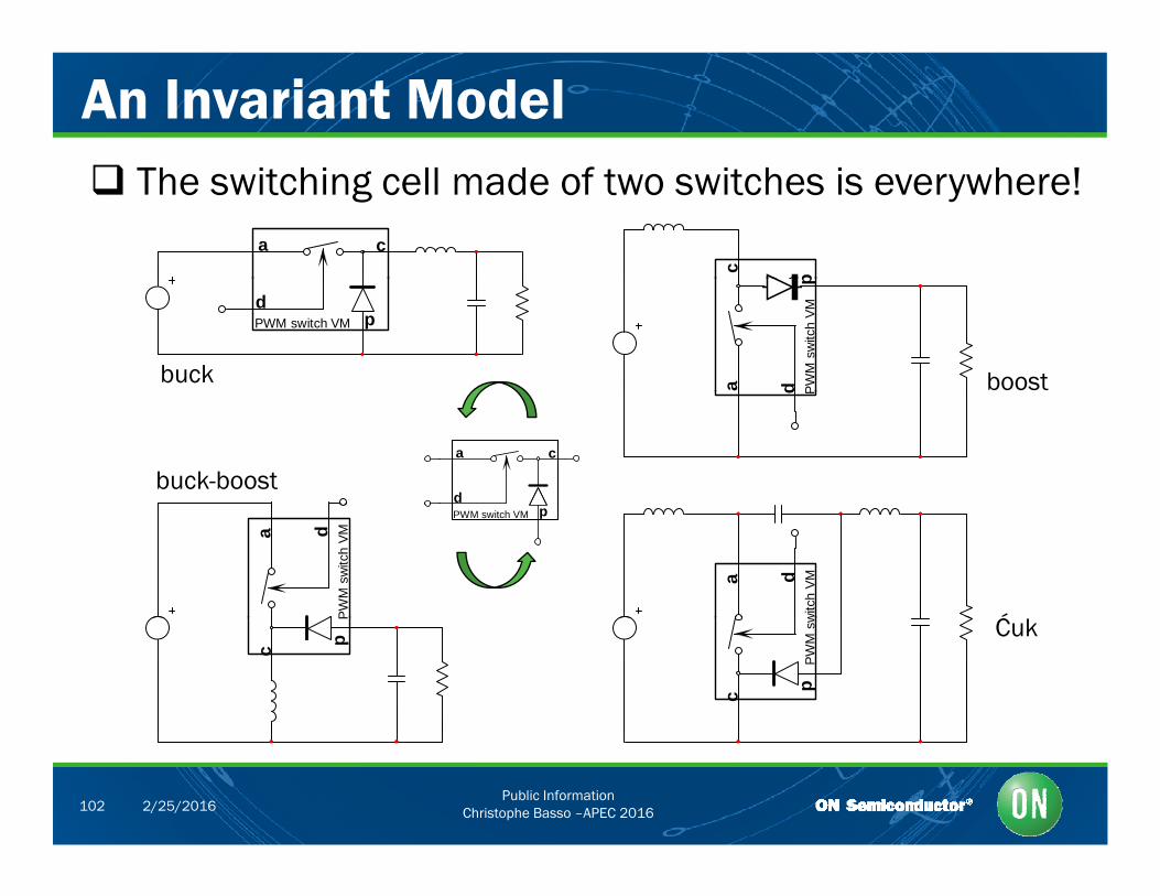
An Invariant Model
a c
c p
The switching cell made of two switches is everywhere!
dPWM switch VM p
da PWM
sw
itch
VMp
buck boostd P
buck-boostd
a c
da
PWM
sw
itch
VM
da
witc
h VM
Ć
PWM switch VM p
c
Pp
c
PWM
sw
p
Ćuk
Public InformationChristophe Basso –APEC 2016102 2/25/2016
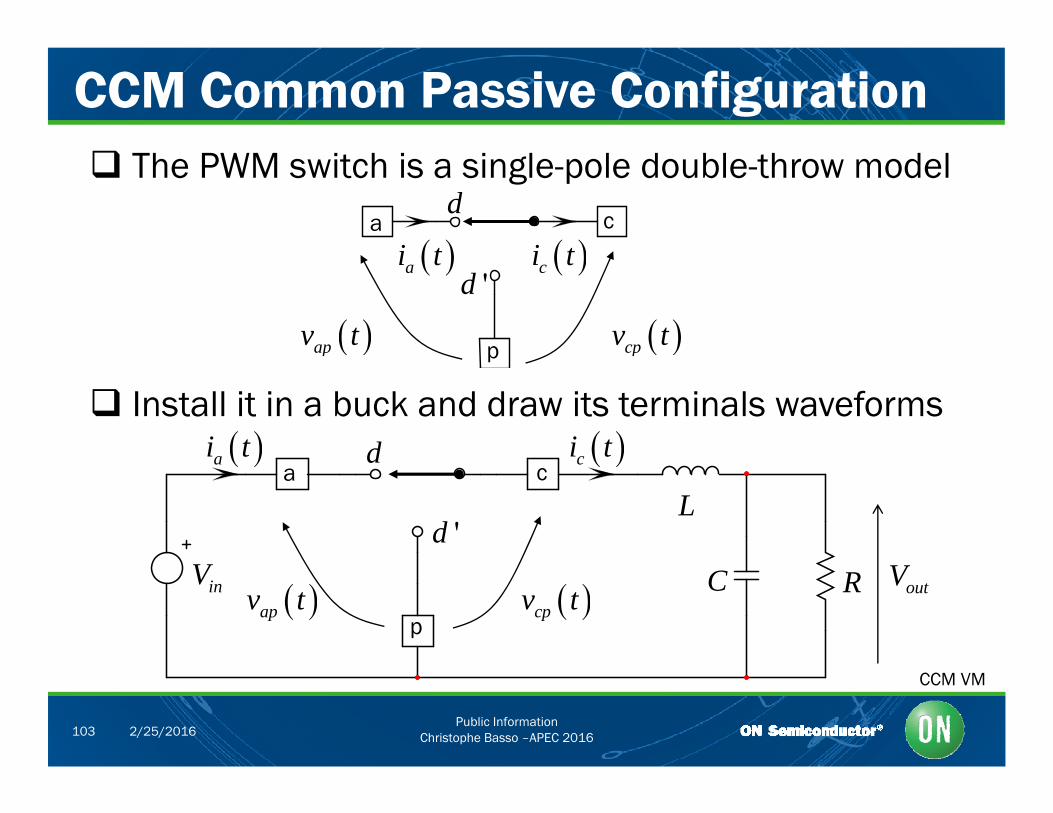
CCM Common Passive Configuration The PWM switch is a single-pole double-throw model
a cd
i t i t
p
'd ai t ci t
apv t cpv t
d ci t ai t Install it in a buck and draw its terminals waveforms
p p p
a cd
'dL
c a
p
C RinV apv t cpv t outV
Public InformationChristophe Basso –APEC 2016103 2/25/2016
CCM VM
The Common Passive Configuration Average the current waveforms across the PWM switch
ci t
swc Ti t
ai t0 t
c Ti t
a cI DI
0 tDT
sw
c T
Averagedvariables
swDT
0
1 sw
sw sw
DT
a a a c cT Tsw
i t I i t dt D i t DIT
Public InformationChristophe Basso –APEC 2016104 2/25/2016
0swCCM VM
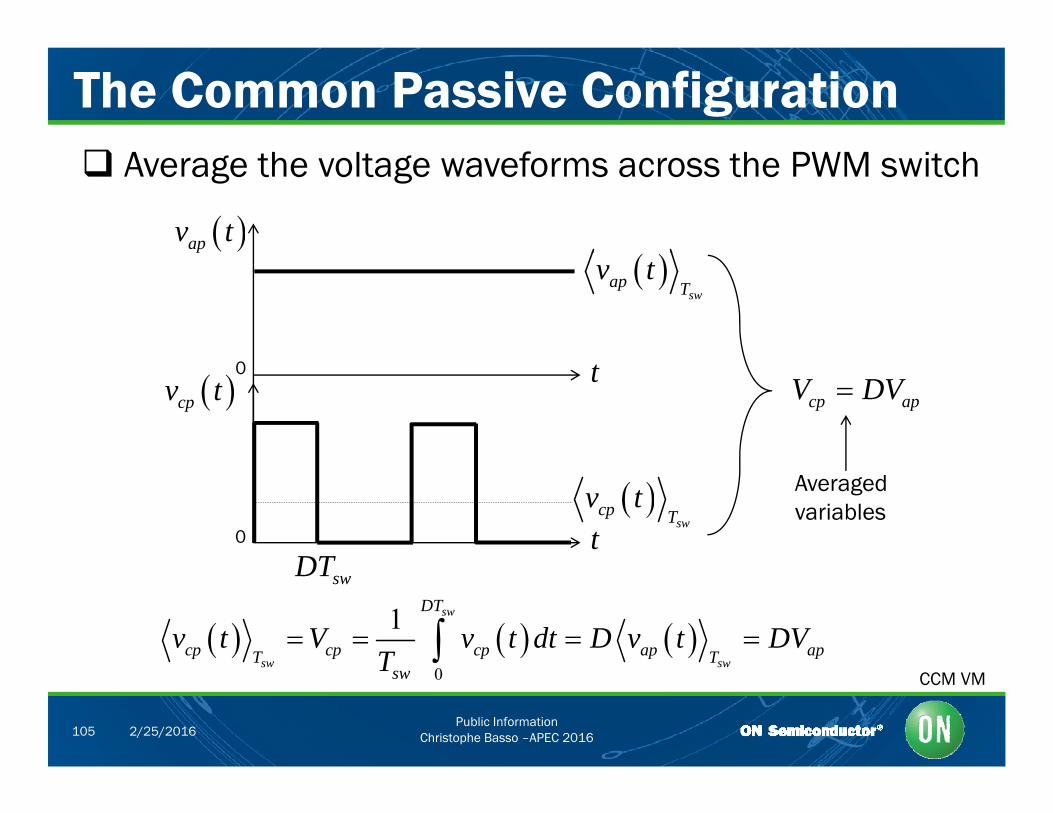
The Common Passive Configuration Average the voltage waveforms across the PWM switch
apv t
swap T
v t
cpv t0 t
cp apV DV
0 tDT
sw
cp Tv t Averaged
variables
swDT
1 sw
sw sw
DT
cp cp cp ap apT Tv t V v t dt D v t DV
T
Public InformationChristophe Basso –APEC 2016105 2/25/2016
CCM VM0sw sw
swT
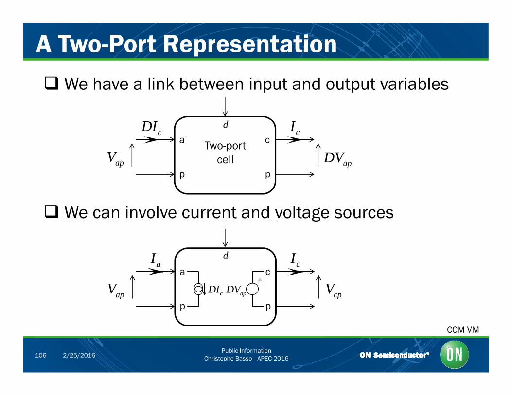
A Two-Port Representation We have a link between input and output variables
DI Id
Two-portcell
a
p
c
p
cDI cI
apDVapV
d
p p
We can involve current and voltage sources
a ccIaI d
a
p
c
papDVapV cpVcDI
Public InformationChristophe Basso –APEC 2016106 2/25/2016
CCM VM
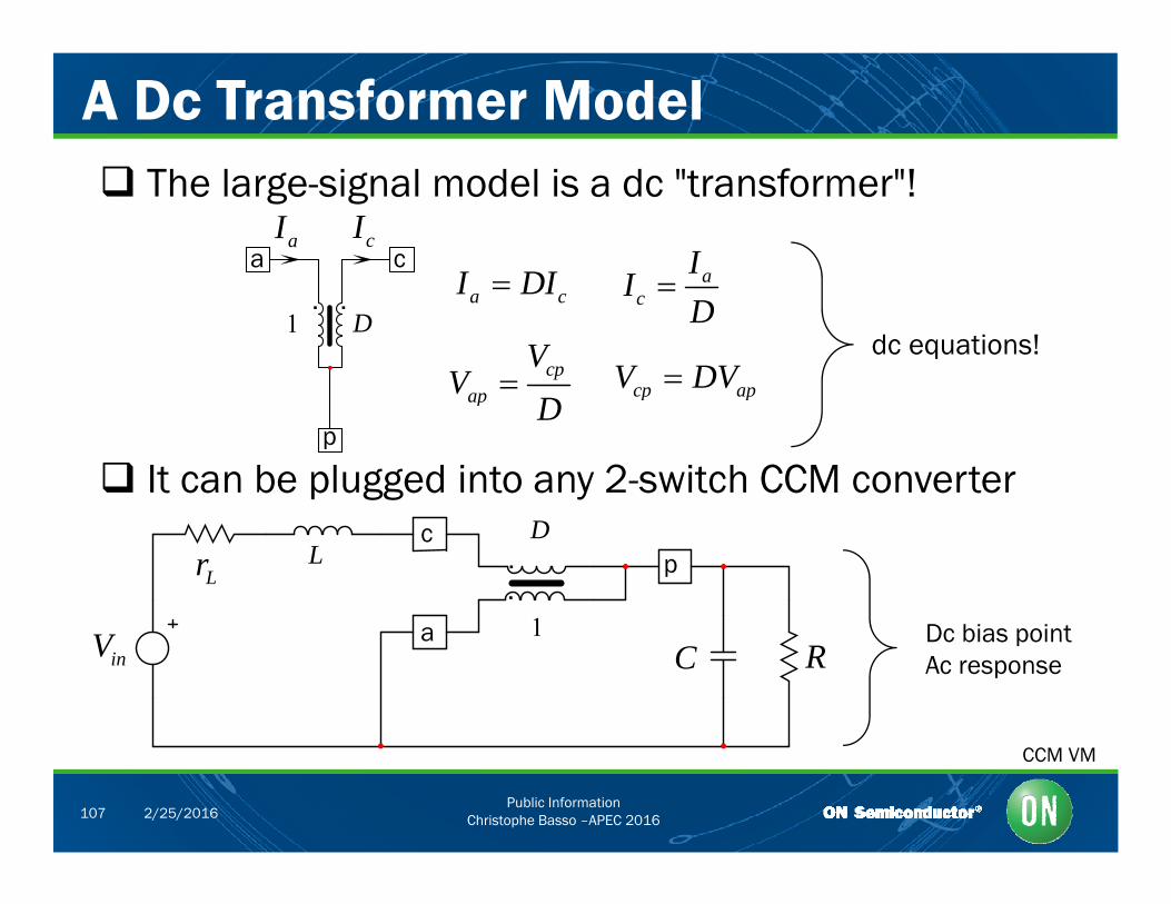
A Dc Transformer Model The large-signal model is a dc "transformer"!
a ccIaI
aIII DI
1 D
acI
Da cI DI
cpap
VV cp apV DV
dc equations!
. .
It can be plugged into any 2-switch CCM converterp
ap Dcp ap
1
D..
LLr
cp
1inV C R
a Dc bias pointAc response
Public InformationChristophe Basso –APEC 2016107 2/25/2016
CCM VM
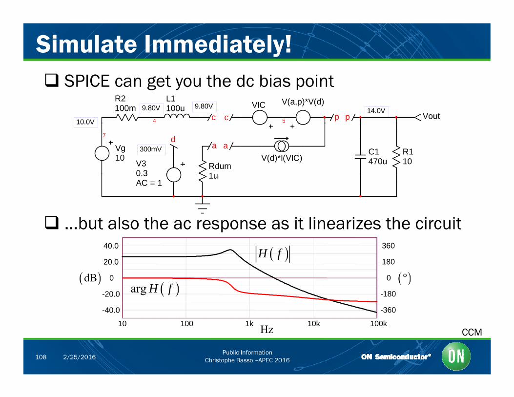
Simulate Immediately! SPICE can get you the dc bias point
4
L1100u
Vout5
VICR2100m
c c
V(a,p)*V(d)
p p9.80V 14.0V
10 0V
9.80V
C1470u
R110
7
Vg10
Rdum1
a aV(d)*I(VIC)V3
0 3
d
10.0V
300mV
1u0.3AC = 1
but also the ac response as it linearizes the circuit
20.0
40.0
180
360
…but also the ac response as it linearizes the circuit
d
H f
-40.0
-20.0
0
10 100 1k 10k 100k
-360
-180
0 dB ° arg H f
Public InformationChristophe Basso –APEC 2016108 2/25/2016
10 100 1k 10k 100kHz CCM
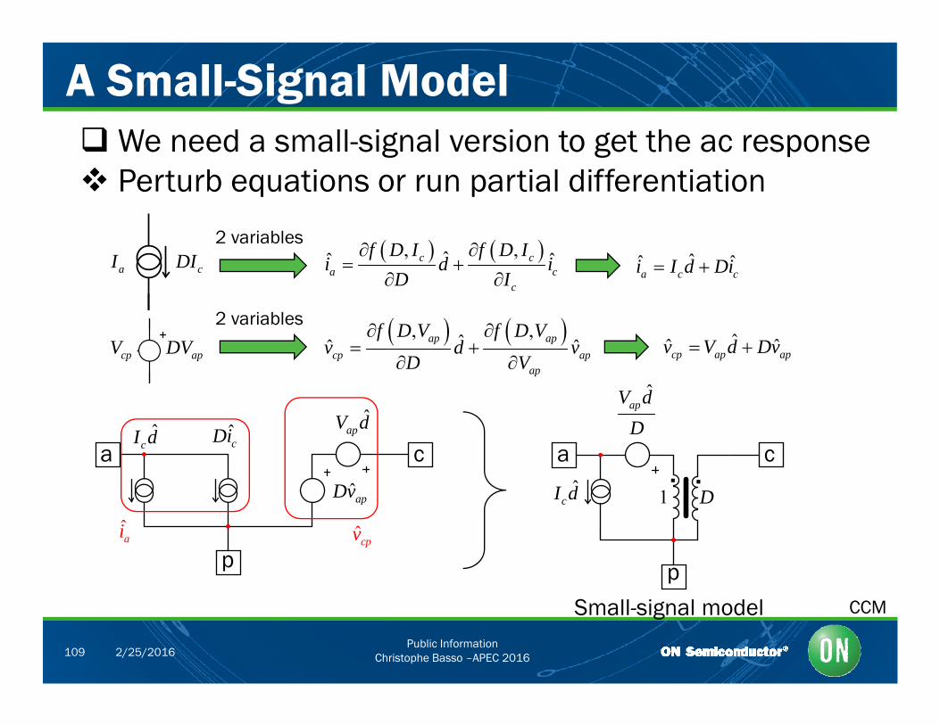
A Small-Signal Model W d ll ig l i t g t th We need a small-signal version to get the ac response Perturb equations or run partial differentiation
cDI , ,ˆˆ ˆc ca c
c
f D I f D Ii d i
D I
2 variables
aI ˆˆ ˆa c ci I d Di
2 variables
apDVcpV , ,ˆˆ ˆap ap
cp apap
f D V f D Vv d v
D V
2 variablesˆˆ ˆcp ap apv V d Dv
ˆapV d
a c a c. .
ˆcI d cDi
ˆcI dˆapDv
ˆapV d
ap
D
1 D
p p
cap
ai ˆcpv
1 D
Public InformationChristophe Basso –APEC 2016109 2/25/2016
Small-signal model CCM

Course Agenda
What is a Transfer Function? Why do We Need New Analytical Techniques? Why do We Need New Analytical Techniques? Time Constants and Poles Identifying the Zeros Identifying the Zeros The Null Double Injection 2nd-Order Networks 2 -Order Networks The PWM Switch Model A CCM Buck in Voltage Mode A CCM Buck in Voltage Mode A CCM Buck-Boost in Voltage Mode
Public InformationChristophe Basso –APEC 2016110 2/25/2016
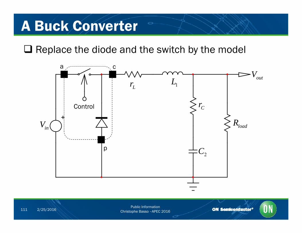
A Buck Converter Replace the diode and the switch by the model
caVoutV
1LLr
Cr
loadRinV
Control
p2C
Public InformationChristophe Basso –APEC 2016111 2/25/2016
Model at Work in a Buck Converter Plug the invariant small-signal model: all linear!
L1100uH
rL10m
B2Voltage
V(a,p)*V(d)/V(D0) Vc
Vi
4
100uH
5
10m
rC30m
R3
Vouta ca
B1CurrentI(Vc)*V(d)
3
B3CurrentI(Vc)*V(D0)
11
B4VoltageV(3,p)*V(D0)
p
c
D012.0V
5.00V 5.00V
4.99V
-582nV
12.0V 5.00V
417mV static
VinVin parameters
Vin=12D=0.417
6
C247uF
R35
pp
V4D
V5AC = 1
d4.99V
0Vdynamic
1µΩ
We want the ac control-to-output transfer function
ˆ 0i
out
v
V sD s
Set node a to 0 V
, inV a p VNode p is ground Simplify schematic
Public InformationChristophe Basso –APEC 2016112 2/25/2016
0inv
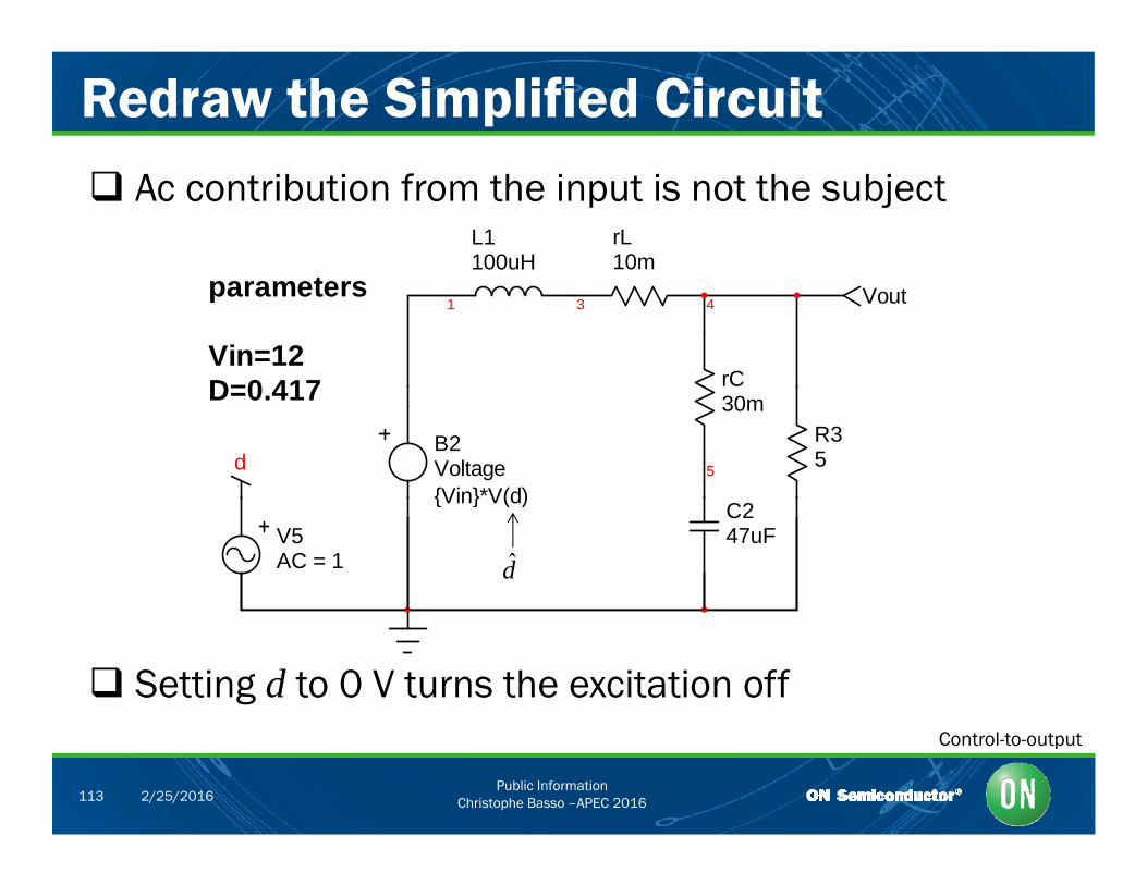
Redraw the Simplified Circuit
L1100uH
rL10m
Ac contribution from the input is not the subject
parameters
Vin=12D=0 417
1 3 4
rC
Vout
D=0.417
5
30mR35
B2VoltageVin*V(d)
d
C247uF
Vin V(d)
V5AC = 1 d
Setting d to 0 V turns the excitation off
Public InformationChristophe Basso –APEC 2016113 2/25/2016
Control-to-output
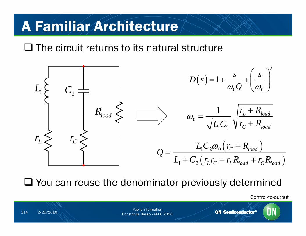
A Familiar Architecture The circuit returns to its natural structure
2s s
1L2C
0 0
1 s sD sQ
loadR0
1 2
1 L load
C load
r Rr RL C
Lr Cr 1 2 0
1 2
C load
L C L load C load
L C r RQ
L C r r r R r R
You can reuse the denominator previously determined
1 2 L C L load C load
Public InformationChristophe Basso –APEC 2016114 2/25/2016
Control-to-output
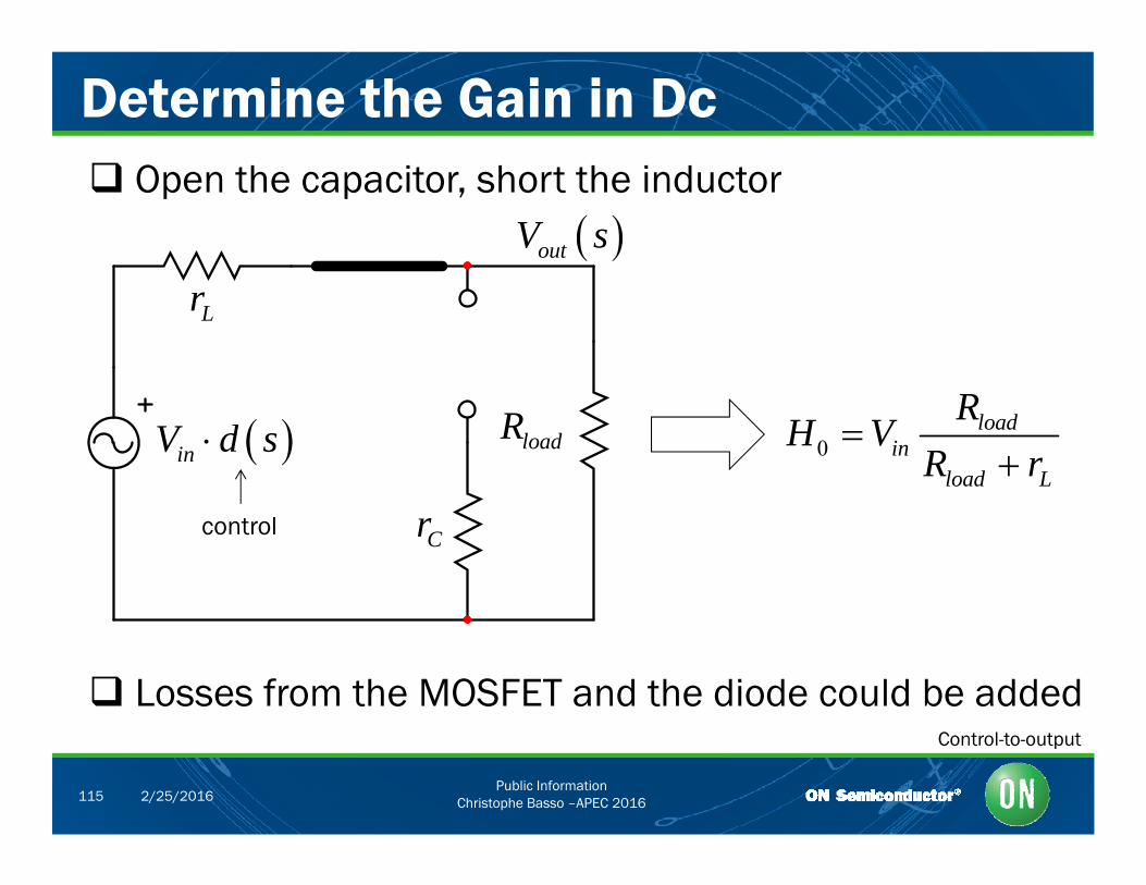
Determine the Gain in Dc Open the capacitor, short the inductor
outV s
Lr
loadR inV d s 0load
inload L
RH V
R r
Crcontrol
Losses from the MOSFET and the diode could be added
Public InformationChristophe Basso –APEC 2016115 2/25/2016
Control-to-output
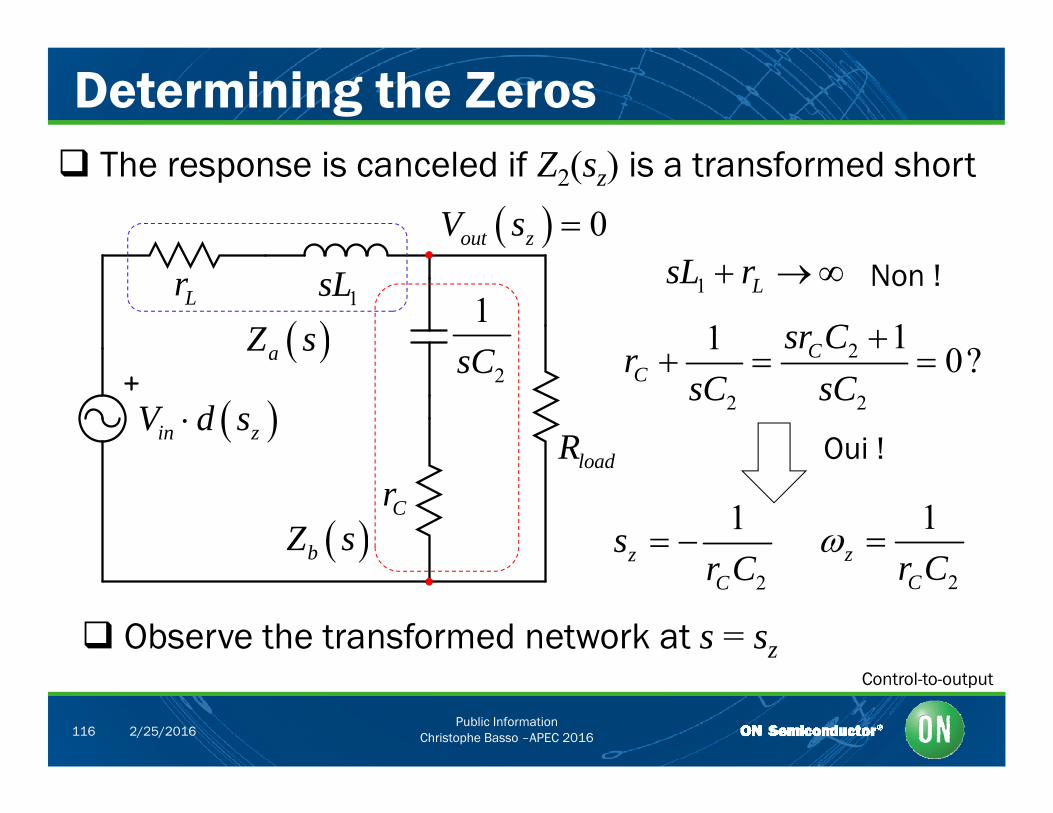
Determining the Zeros The response is canceled if Z2(sz) is a transformed short
0out zV s
Lr 1sL1C
1 LsL r Non !
2 11 0?Csr C aZ s
l dR in zV d s
2sC 2
2 2
0?CCr sC sC
Oui !
a
CrloadR Oui !
1zs
C
1z C
bZ s
Observe the transformed network at s = sz
2z
Cr C 2z
Cr C
Public InformationChristophe Basso –APEC 2016116 2/25/2016
Control-to-output
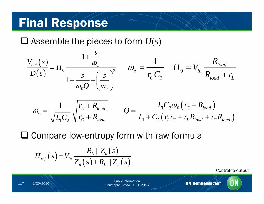
Final Response Assemble the pieces to form H(s)
1 sV s
l dR1
0 2
0 0
1
out zV sH
D s s sQ
0load
inload L
RH V
R r
2
1z
Cr C
0 0Q
01 L loadr R
RL C
1 2 0 C loadL C r R
QL C R R
0
1 2 C loadr RL C 1 2 L C L load C loadL C r r r R r R
Compare low-entropy form with raw formula
|| Z|| Z
L bref in
a L b
R sH s V
Z s R s
Public InformationChristophe Basso –APEC 2016117 2/25/2016
Control-to-output
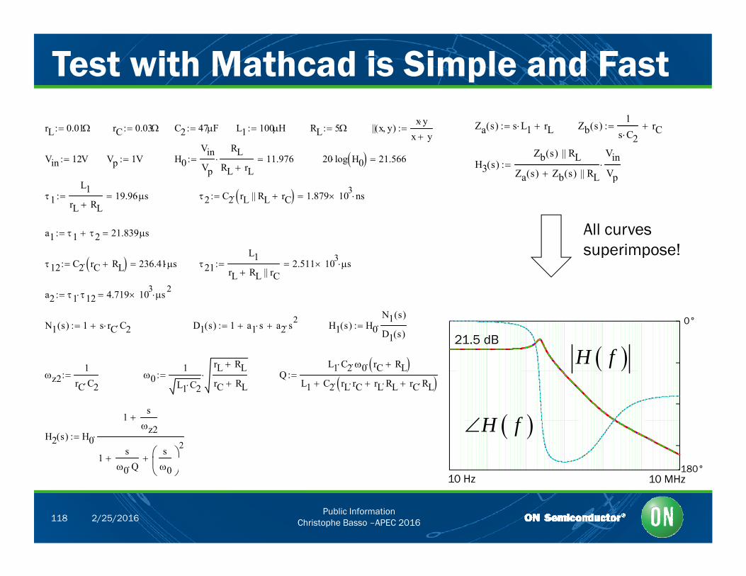
Test with Mathcad is Simple and FastrL 0.01 rC 0.03 C2 47F L1 100H RL 5 || x y( )
x yx y
Vin 12V Vp 1V H0VinVp
RLRL rL 11.976 20 log H0 21.566
Za s( ) s L1 rL Zb s( )1
s C2rC
H3 s( )Zb s( ) || RL
Za s( ) Zb s( ) || RL
VinVp
All curvessuperimpose!
1L1
rL RL19.96s 2 C2 rL || RL rC 1.879 103
ns
a1 1 2 21.839s
L
a b L p
superimpose!
0°
12 C2 rC RL 236.41s 21L1
rL RL || rC2.511 103
s
a2 1 12 4.719 103 s 2
N s( ) 1 s r C D s( ) 1 a s a s2 H s( ) H
N1 s( )
H f21.5 dB
N1 s( ) 1 s rC C2 D1 s( ) 1 a1 s a2 s H1 s( ) H0 D1 s( )
z21
rC C2 0
1
L1 C2
rL RL
rC RL Q
L1 C2 0 rC RL
L1 C2 rL rC rL RL rC RL
H f
-180°
H2 s( ) H0
1sz2
1s
0 Q
s0
2
Public InformationChristophe Basso –APEC 2016118 2/25/2016
10 Hz 10 MHz-1800 Q 0
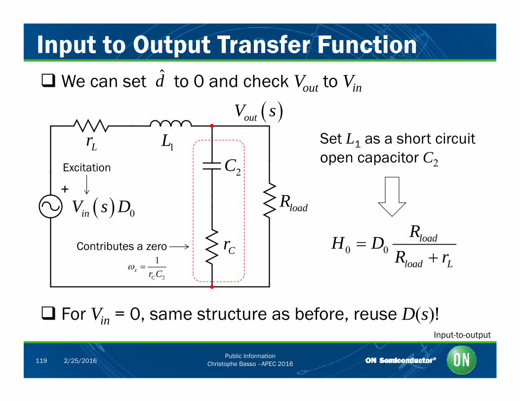
Input to Output Transfer Function ˆ We can set to 0 and check Vout to Vin
outV s
d
Lr 1L
2CSet L1 as a short circuitopen capacitor C2Excitation
loadR 0inV s D
2
RCr 0 0
load
load L
RH D
R r
Contributes a zero
2
1z
Cr C
For Vin = 0, same structure as before, reuse D(s)!
2Cr C
Public InformationChristophe Basso –APEC 2016119 2/25/2016
Input-to-output
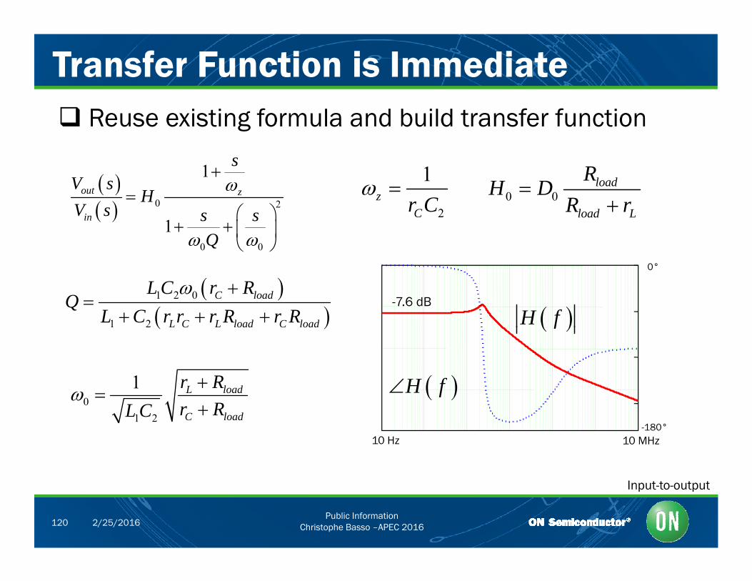
Transfer Function is Immediate
1 sV
loadR
H D1
Reuse existing formula and build transfer function
0 2
0 0
1
out z
in
V sH
V s s sQ
0 0load
load L
H DR r
2
1z
Cr C
1 2 0
1 2
C load
L C L load C load
L C r RQ
L C r r r R r R
H f
0°
-7.6 dB
01 L loadr R
C load C load f
H f0
1 2 C loadr RL C
10 Hz 10 MHz
-180°
Public InformationChristophe Basso –APEC 2016120 2/25/2016
Input-to-output
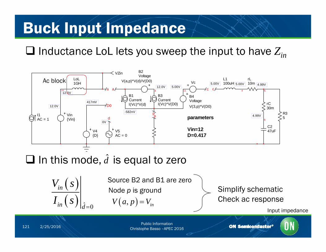
Buck Input Impedance Inductance LoL lets you sweep the input to have Zin
L1 rLLoLVZin B2
Voltage
10 4
L1100uH
5
rL10m
rC30m
a c
LoL1GH
a
B1CurrentI(Vc)*V(d)
3
V(a,p)*V(d)/V(D0)
B3CurrentI(Vc)*V(D0)
11
B4VoltageV(3,p)*V(D0)
Vc
c
D0
12.0V
5.00V 5.00V 4.99V12.0V 5.00V
417mV12.0V
Ac block
VinVin parameters
Vin=12D=0.417
6
C247uF
R35
I1AC = 1
pp
V4D
d
V5AC = 0
4.99V-582nV
0V
In this mode, is equal to zerod
ˆ 0
in
in d
V sI s
Source B2 and B1 are zero
, inV a p VNode p is ground Simplify schematic
Check ac response
Public InformationChristophe Basso –APEC 2016121 2/25/2016
0in d inp
Input impedance
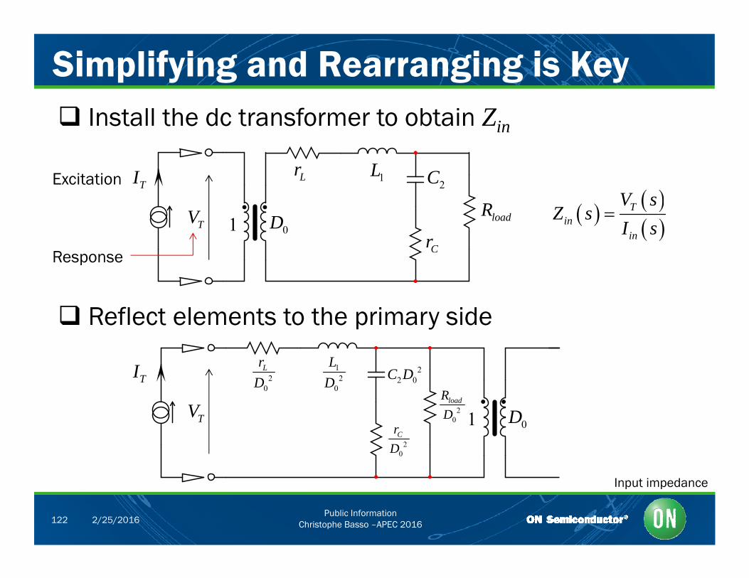
Simplifying and Rearranging is Key Install the dc transformer to obtain Zin
CLr 1LIExcitation
Cr
2C
loadR
L 1TI
TV 1 0D
Tin
in
V sZ s
I s
Excitation
R
Reflect elements to the primary side
Response
p y
22 0C D
l dR2
0
LrD
12
0
LDTI
1 0D20
loadRD
20
CrD
TV
Public InformationChristophe Basso –APEC 2016122 2/25/2016
Input impedance
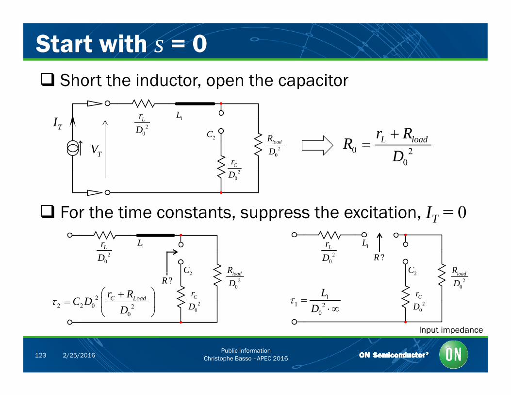
Start with s = 0 Short the inductor, open the capacitor
LrI 1L
20
loadRD
2Cr
D
20DTI
TV 0 20
L loadr RR
D
2C
20D
For the time constants, suppress the excitation, IT = 0
l dR
20
LrD
l dR
20
LrD ?R
2C
1L
2C
1L
20
loadRD
20
CrD
?R
22 2 0 2
0
C Loadr RC D
D
20
loadRD
20
CrD
11 2
0
LD
2C 2C
Public InformationChristophe Basso –APEC 2016123 2/25/2016
Input impedance
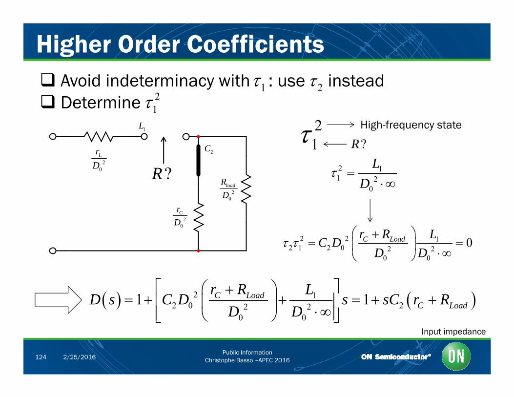
Higher Order Coefficients Avoid indeterminacy with : use instead Determine
1 221
2L High frequency state21
?R2
0
LrD
1L
2C
High-frequency state
?R
2 1L ?R
20
loadRD
2Cr
D
1 20D
0D
2 2 12 1 2 0 2 2
0 0
0C Loadr R LC D
D D
2 12 0 22 2
0 0
1 1C LoadC Load
r R LD s C D s sC r R
D D
Public InformationChristophe Basso –APEC 2016124 2/25/2016
Input impedance
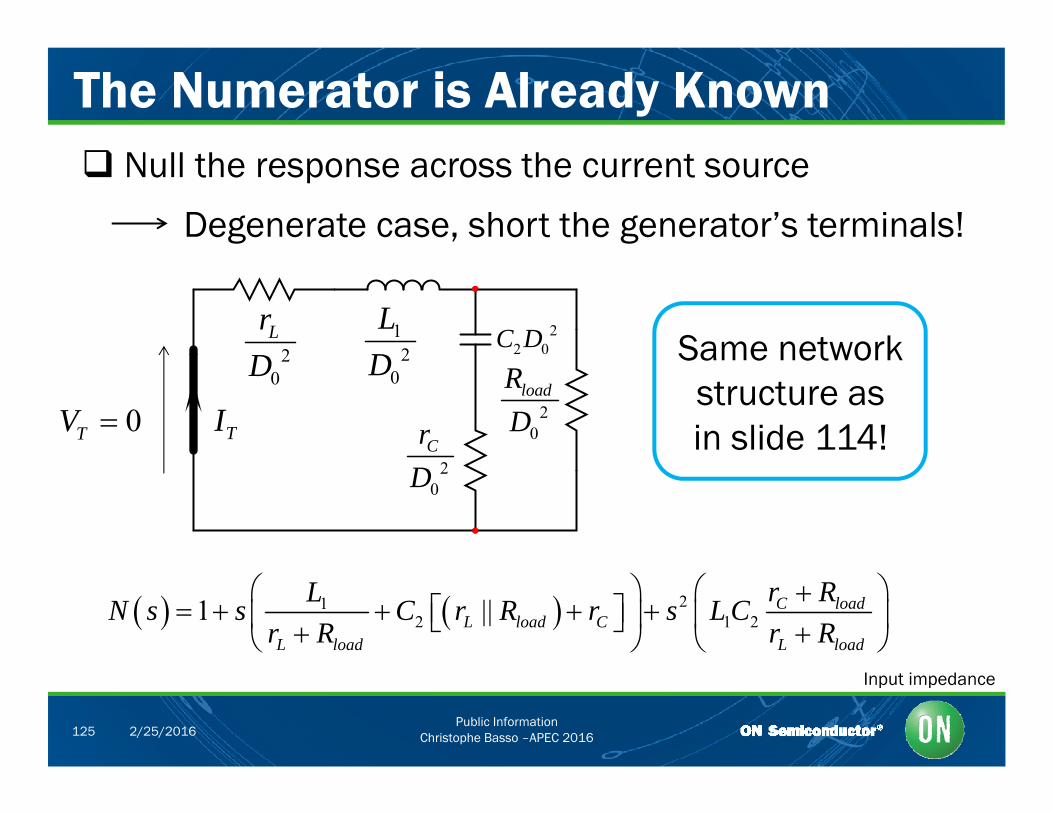
The Numerator is Already Known Null the response across the current source
Degenerate case, short the generator’s terminals!
2Lr
D Same network 2
2 0C D12
LD
20
loadRD
Cr
20D
TI
Same network structure asin slide 114!0TV
20D
20D
212 1 21 || C load
L load CL load L load
r RLN s s C r R r s L Cr R r R
Public InformationChristophe Basso –APEC 2016125 2/25/2016
Input impedance
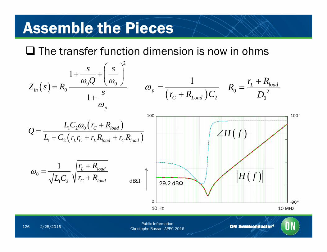
Assemble the Pieces
2
1 s sQ
R1
The transfer function dimension is now in ohms
0 00
1in
p
QZ s R s
0 2
0
L loadr RR
D
2
1p
C Loadr R C
1 2 0
1 2
C load
L C L load C load
L C r RQ
L C r r r R r R
H f
100°100
01 L loadr R
C load C load
H f01 2 C loadr RL C H f
-90°
29.2 dBΩdBΩ
0
Public InformationChristophe Basso –APEC 2016126 2/25/2016
10 Hz 10 MHz

Course Agenda
What is a Transfer Function? Why do We Need New Analytical Techniques? Why do We Need New Analytical Techniques? Time Constants and Poles Identifying the Zeros Identifying the Zeros The Null Double Injection 2nd-Order Networks 2 -Order Networks The PWM Switch Model A CCM Buck in Voltage Mode A CCM Buck in Voltage Mode A CCM Buck-Boost in Voltage Mode
Public InformationChristophe Basso –APEC 2016127 2/25/2016
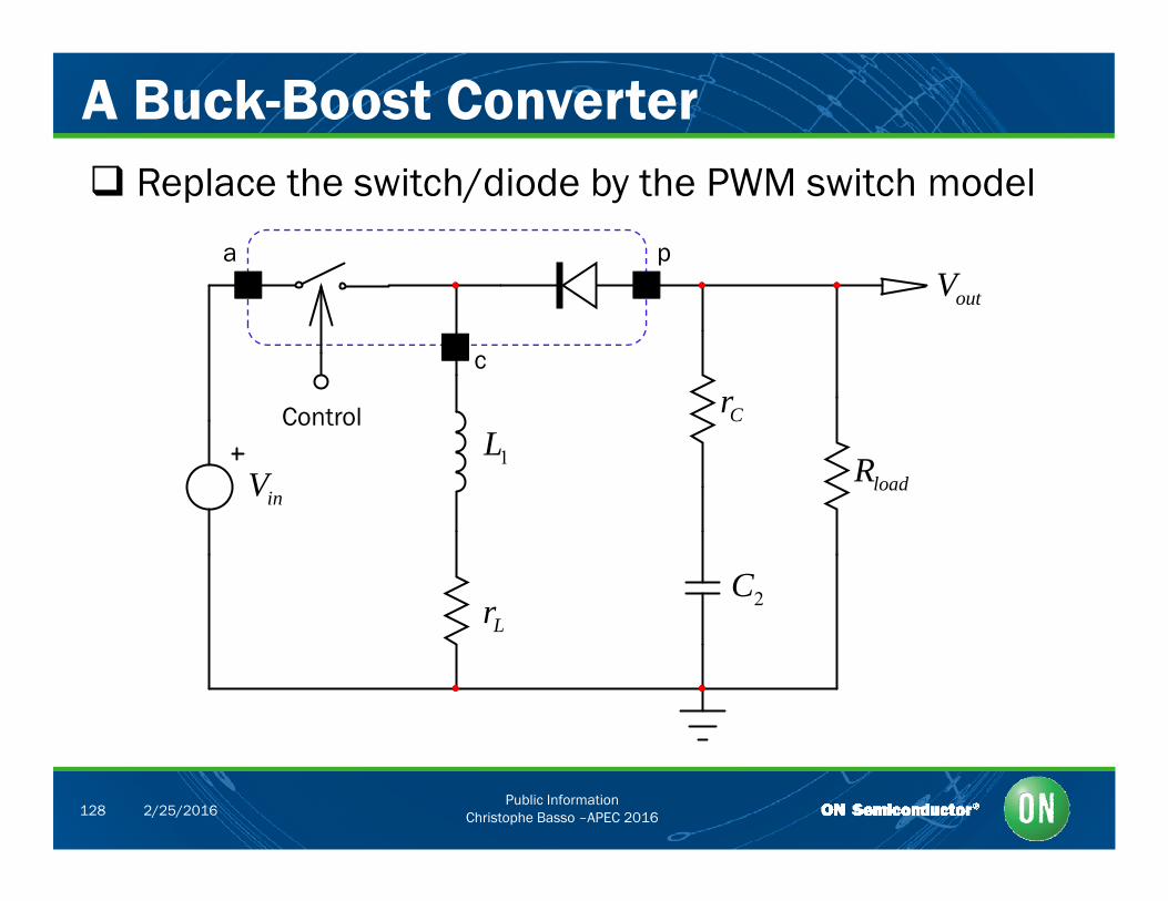
A Buck-Boost Converter Replace the switch/diode by the PWM switch model
a pV
c
outV
Cr
loadR1LinV
Control
Lr2C
Lr
Public InformationChristophe Basso –APEC 2016128 2/25/2016
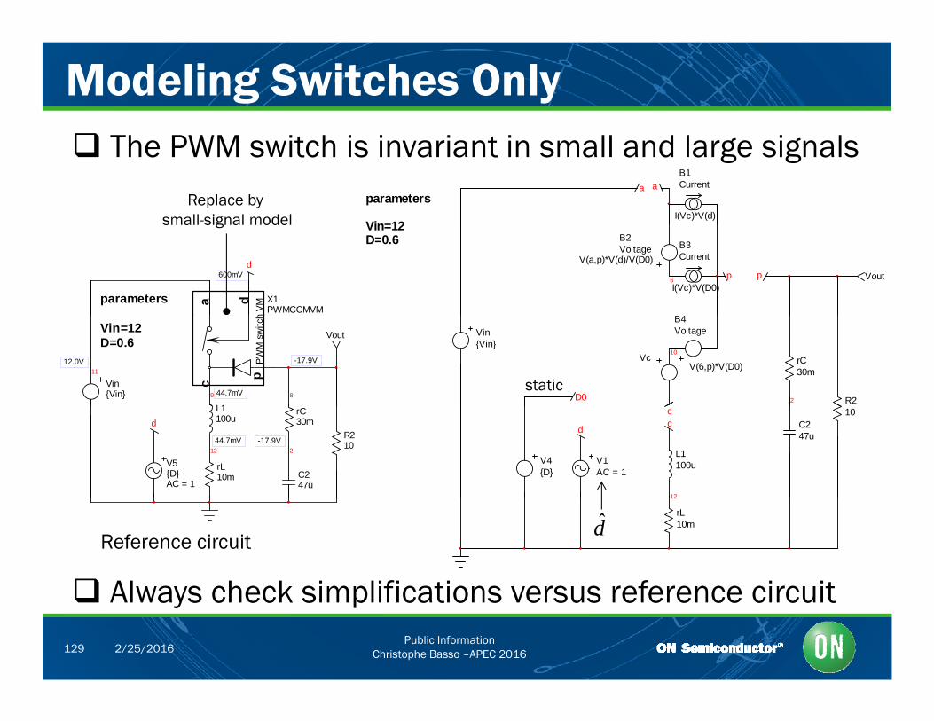
Modeling Switches Only The PWM switch is invariant in small and large signals
aparameters
Vin=12
aB1Current
I(Vc)*V(d)Replace by
small-signal model
p Vout
Vin=12D=0.6
6
B2Voltage
V(a,p)*V(d)/V(D0)B3Current
I(Vc)*V(D0)p
parameters da
h VM
X1PWMCCMVM
d600mV
small signal model
2
rC30m
R2
VinVin
D0
10
B4Voltage
V(6,p)*V(D0)Vc
9
L18
11
VinVin
VoutVin=12D=0.6
c
PWM
sw
itch
p
44.7mV
-17.9V12.0V
static
12
L1100u
C247u
10c
V4D
c
V1AC = 1
d
12
L1100u
2
rC30m
C247u
R210
rL10m
V5DAC = 1
d
-17.9V44.7mV
Always check simplifications versus reference circuit
12
rL10m
Reference circuitd
Public InformationChristophe Basso –APEC 2016129 2/25/2016
Always check simplifications versus reference circuit
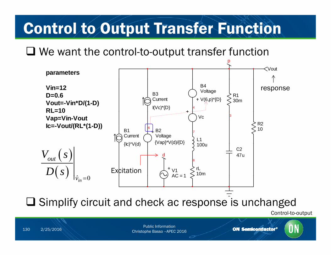
Control to Output Transfer Function
p
Voutparameters
We want the control-to-output transfer function
R130m
Vin=12D=0.6Vout=-Vin*D/(1-D)RL=10
B3Current
I(Vc)*D 4
B4Voltage
V(6,p)*D
response
7
L1100
3
R210
RL=10Vap=Vin-VoutIc=-Vout/(RL*(1-D))
B1Current
Ic*V(d)
6B2VoltageVap*V(d)/D
Vc
8
100uC147u
Ic V(d) Vap V(d)/D
V1AC = 1
d
rL10m
ˆ 0
outV sD s
C247u
ExcitationAC = 1 ˆ 0inv
Simplify circuit and check ac response is unchanged
Public InformationChristophe Basso –APEC 2016130 2/25/2016
gControl-to-output
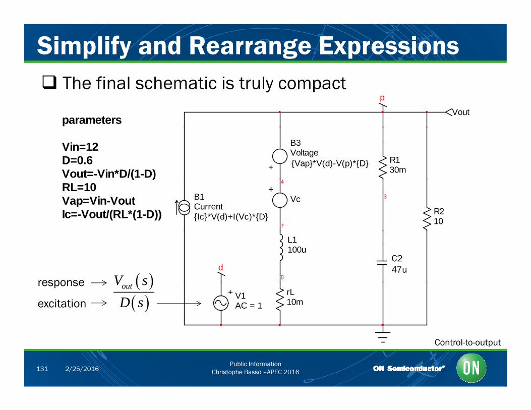
Simplify and Rearrange Expressions
p
Voutparameters
The final schematic is truly compact
R130m
Vin=12D=0.6Vout=-Vin*D/(1-D)
B3VoltageVap*V(d)-V(p)*D
7
3
R210
( )RL=10Vap=Vin-VoutIc=-Vout/(RL*(1-D))
B1CurrentIc*V(d)+I(Vc)*D
4
Vc
8
L1100u C1
47udC247u
V sresponseV1AC = 1
rL10m
outV sD s
response
excitation
Public InformationChristophe Basso –APEC 2016131 2/25/2016
Control-to-output
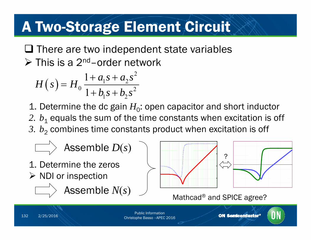
A Two-Storage Element Circuit There are two independent state variables This is a 2nd–order network
21 2
1 20 2
1 2
11
a s a sH s H
b s b s
1 Determine the dc gain H : open capacitor and short inductor1. Determine the dc gain H0: open capacitor and short inductor2. b1 equals the sum of the time constants when excitation is off3. b2 combines time constants product when excitation is off
Assemble D(s)1 Determine the zeros
?1. Determine the zeros NDI or inspection
Assemble N(s)M th d® d SPICE g ?
Public InformationChristophe Basso –APEC 2016132 2/25/2016
( )Mathcad® and SPICE agree?
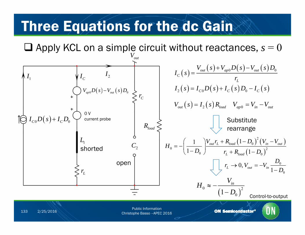
Three Equations for the dc Gain
I
outV
0 0out ap outV s V D s V s DI s
Apply KCL on a simple circuit without reactances, s = 0
CI1I 2I
Cr 0 0ap outV D s V s D
CL
I sr
2 0 0C C CI s I D s I s D I s
V I R V V V
0 0C CI D s I DloadR
2out loadV s I s R
Substituterearrange
0 Vcurrent probe
0ap in outV V V
1L2C
open
shorted
20
0 20 0
111 1
out L load in out
L load
V r R D V VH
D r R D
D
Lropen
0 21inV
HD
0
0
0,1L out in
Dr V V
D
Public InformationChristophe Basso –APEC 2016133 2/25/2016
01 DControl-to-output
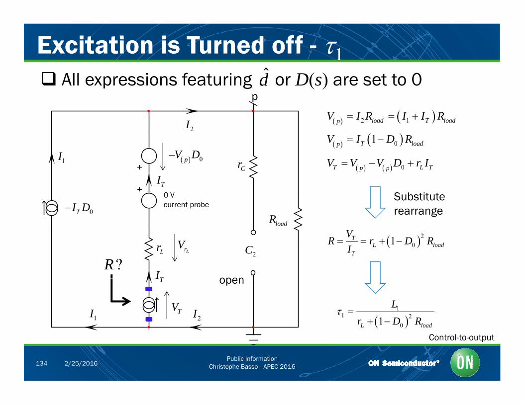
Excitation is Turned off - 1 All i f t i D( ) t t 0d All expressions featuring or D(s) are set to 0d
I
p
2 1load T loadpV I R I I R
1I
I
2I
Cr 0pV D
0T L Tp pV V V D r I
01T loadpV I D R
TI
loadR0TI D
Substituterearrange
0 Vcurrent probe
TI
Lr 2
01TL load
T
VR r D R
I
?RLr
V2C
openTI
2I1I TV
11 2
01L load
Lr D R
open
Public InformationChristophe Basso –APEC 2016134 2/25/2016
Control-to-output
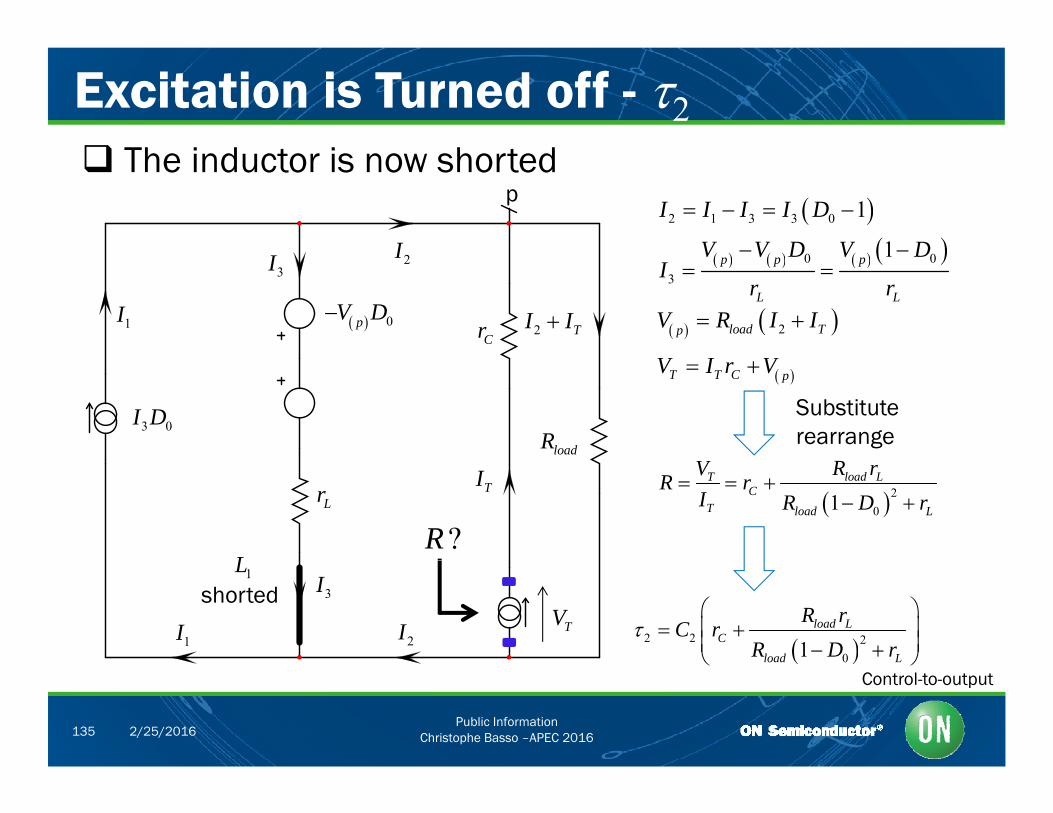
Excitation is Turned off - 2 Th i d t i h t d
I
p 2 1 3 3 0 1I I I I D
1V V D V D
The inductor is now shorted
1I
2I
Cr 0pV D
3I
2 TI I
0 03
1p p p
L L
V V D V DI
r r
2load TpV R I I
loadR3 0I D
T T C pV I r V
Substituterearrange
TI
?RLr 2
01load LT
CT load L
R rVR r
I R D r
L
TV3I
1I 2I 2 2 2
01load L
Cload L
R rC r
R D r
1Lshorted
Public InformationChristophe Basso –APEC 2016135 2/25/2016
Control-to-output
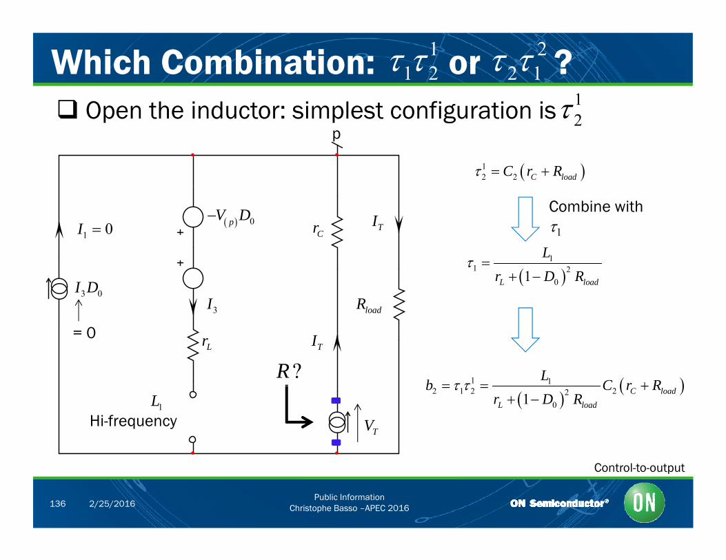
Which Combination: or ? O th i d t i l t fi ti i
11 2
1
22 1
Open the inductor: simplest configuration is p
12 2 C l dC r R
12
1 0I 0pV DTI
Cr
2 2 C loadC r R
Combine with1
loadR3 0I D
3I
1
1 201L load
Lr D R
TI
?RLr
1 1Lb C r R
= 0
TV
2 1 2 2201
C loadL load
b C r Rr D R
1LHi-frequency
Public InformationChristophe Basso –APEC 2016136 2/25/2016
Control-to-output
Denominator Expression
1 l d LR rL
The 2nd-order denominator can be formed
1
1 1 2 22 20 01 1
load LC
L load load L
R rLb C r
r D R R D r
L
1 1
2 1 2 2201
C loadL load
Lb C r R
r D R
RL L
21 1
2 22 2 20 0 0
11 1 1
load LC C load
L load load L L load
R rL LD s C r s C r R s
r D R R D r r D R
N
0 21 21N s
H s Hb s b s
Zeros are missing!
Public InformationChristophe Basso –APEC 2016137 2/25/2016
Control-to-output
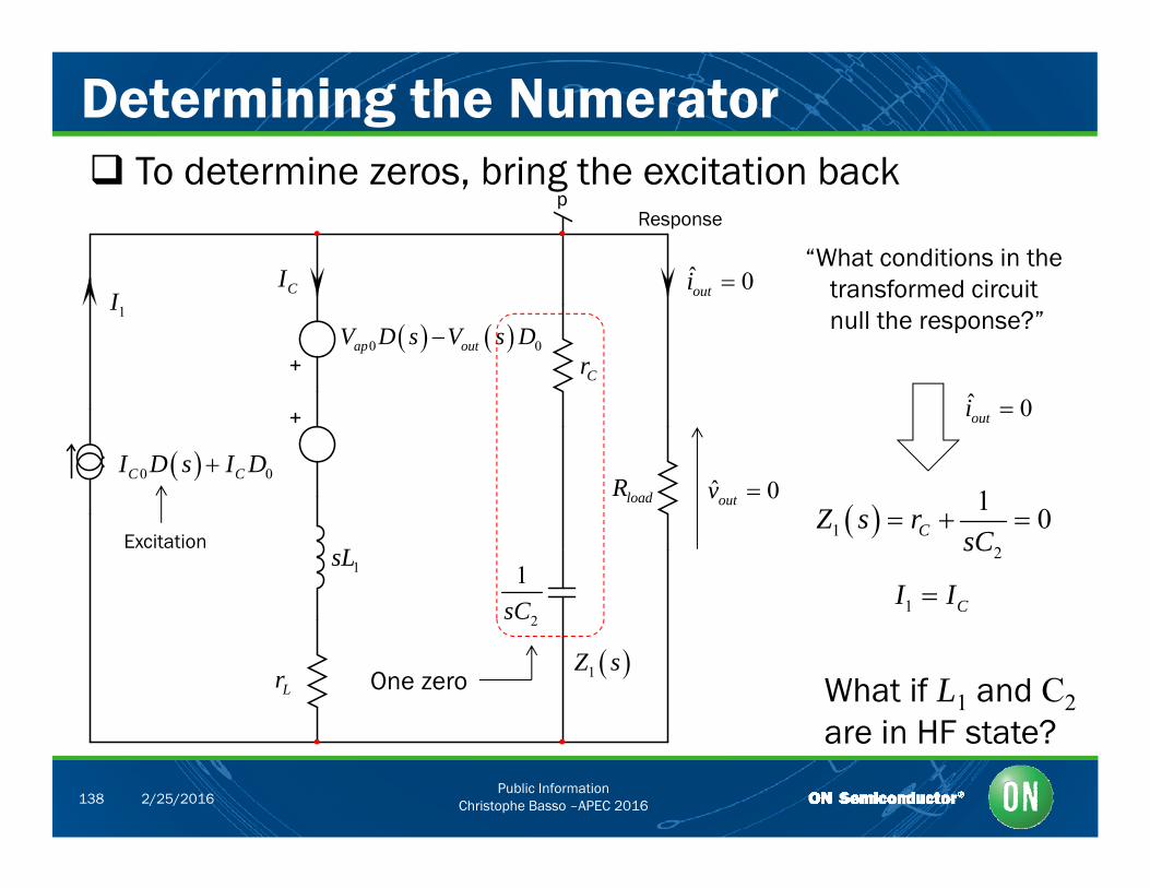
Determining the Numerator To determine zeros bring the excitation back To determine zeros, bring the excitation back
p
I ˆ 0i“What conditions in the
Response
CI1I
0outi
Cr 0 0ap outV D s V s D
transformed circuit null the response?”
0 0C CI D s I DloadR ˆ 0outv 1
ˆ 0outi
load
1sL1
sC
out
12
1 0CZ s rsC
1 CI I
Excitation
Lr
2sC
1Z sWhat if L1 and C2
i HF t t ?
One zero
Public InformationChristophe Basso –APEC 2016138 2/25/2016
are in HF state?
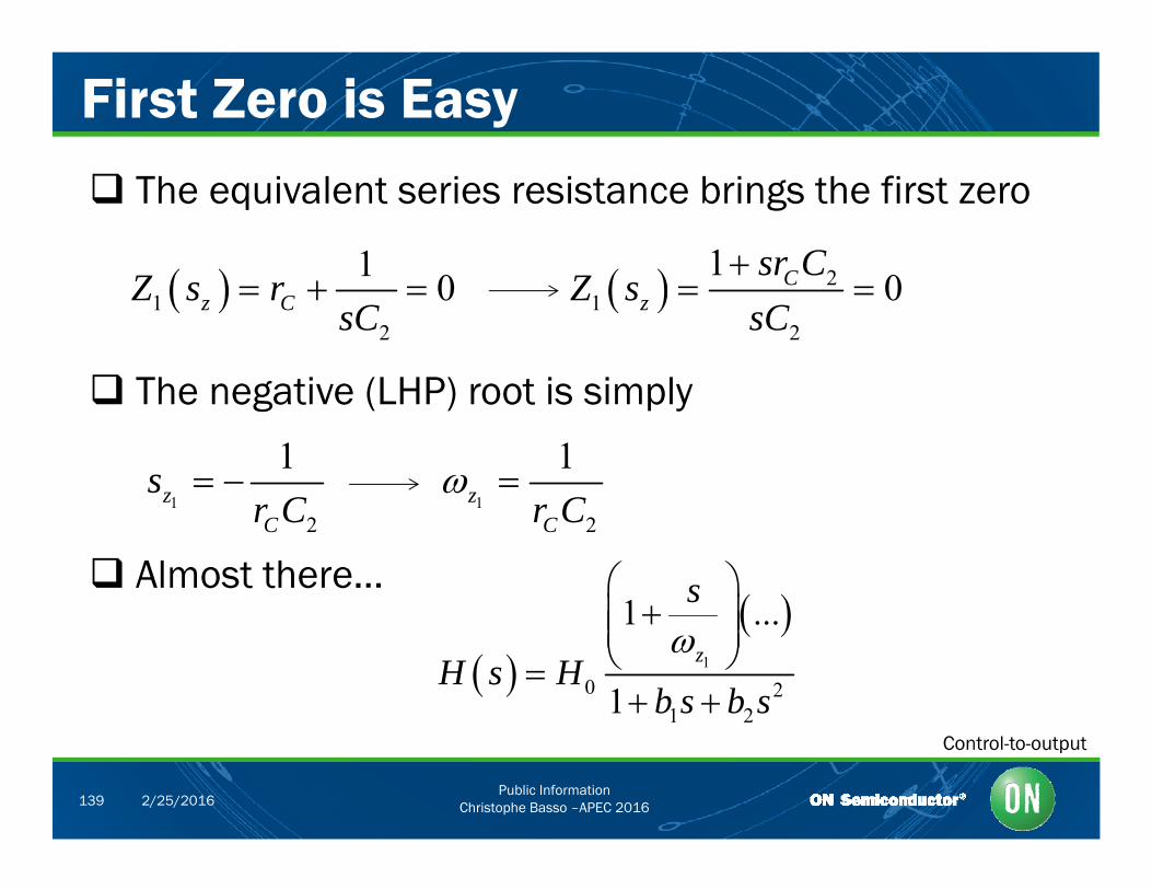
First Zero is Easy The equivalent series resistance brings the first zero
1 0Z 210Csr C
Z 1
2
0z CZ s rsC
21
2
0CzZ s
sC
The negative (LHP) root is simply The negative (LHP) root is simply
1
1zs
C
1
1z C
1
2z
Cr C 12
zCr C
Almost there… 1 s
1
0 21 2
1 ...
1zH s H
b s b s
Public InformationChristophe Basso –APEC 2016139 2/25/2016
Control-to-output
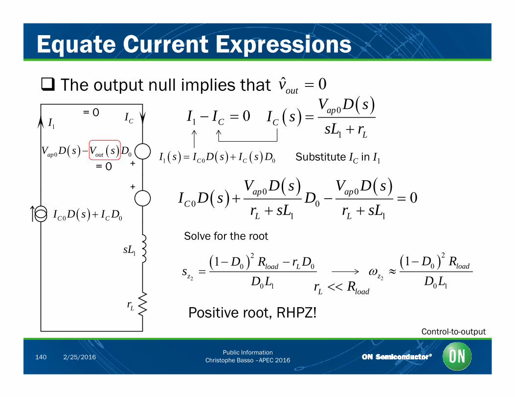
Equate Current Expressions The output null implies that ˆ 0outv
= 0CII 1 0CI I 0ap
C
V D sI s
L
1I
0 0ap outV D s V s D
1 C 1
CLsL r
= 0 1 0 0C CI s I D s I s D Substitute IC in I1
0 0C CI D s I D 0 0
0 01 1
0ap apC
L L
V D s V D sI D s D
r sL r sL
1sLSolve for the root
20 01 load LD R r D
s
2
01 loadD R
Lr
20 1
zsD L
Positive root, RHPZ!
L loadr R2
0 1z D L
Public InformationChristophe Basso –APEC 2016140 2/25/2016
Control-to-output
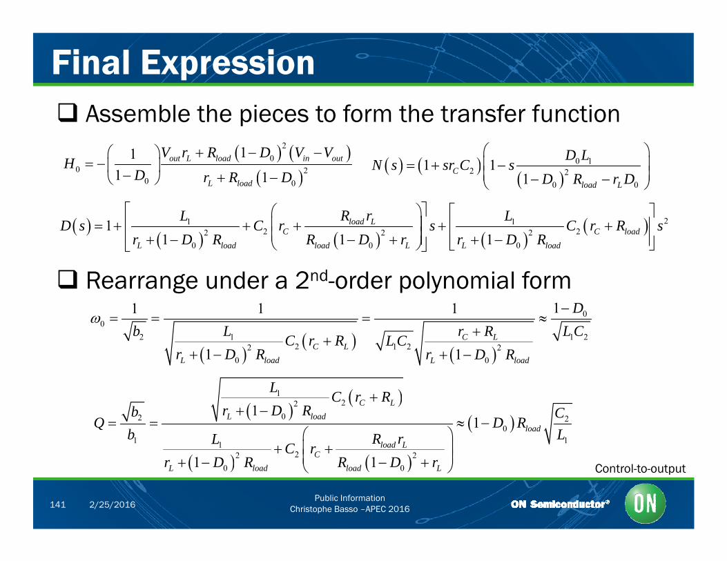
Final Expression Assemble the pieces to form the transfer function
20
0 2
111 1
out L load in outV r R D V VH
D R D
0 1
2 21 11
CD L
N s sr C sD R D
21 12 22 2 2
0 0 0
11 1 1
load LC C load
L load load L L load
R rL LD s C r s C r R s
r D R R D r r D R
0 01 1L load
D r R D
20 01 load LD R r D
0 0 0L load load L L load
Rearrange under a 2nd-order polynomial form011 1 1 D
00
2 1 1 22 1 22 2
0 01 1C L
C LL load L load
b L r R L CC r R L Cr D R r D R
L
122
02 20
1 1122 2
11
1 1
C LL load
load
load LC
L C r Rr D Rb C
Q D Rb LR rL C r
D R R D
Public InformationChristophe Basso –APEC 2016141 2/25/2016
2 20 01 1L load load Lr D R R D r Control-to-output
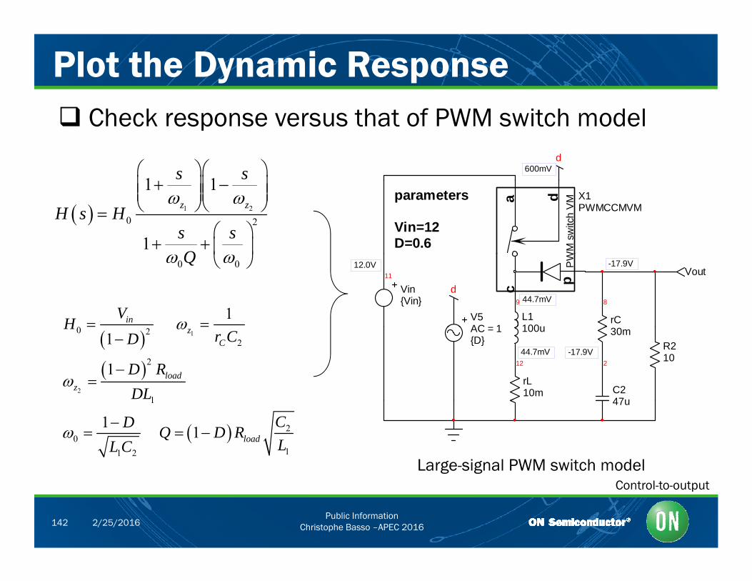
Plot the Dynamic Response
1 1s s
Check response versus that of PWM switch modeld
600mV
1 2
0 2
1 1
1
z zH s Hs sQ
parameters
Vin=12D=0.6
da
WM
sw
itch
VM X1
PWMCCMVM
0 0Q
01inV
H 9
L1100u
8
rC
11
VinVin
Vout
c
PW
p
V5AC = 1
d44.7mV
-17.9V12.0V
1
2
0 22
2
1
1
1
zC
loadz
Hr CD
D RDL
12
100u
2
30m
C247u
R210
rL10m
AC = 1D
-17.9V44.7mV
1
20
11 2
1 1 loadCD Q D RLL C
47u
Large-signal PWM switch model
Public InformationChristophe Basso –APEC 2016142 2/25/2016
Control-to-output
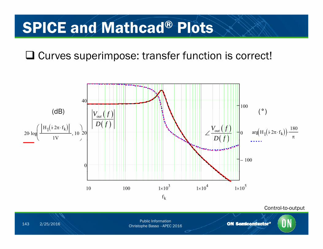
SPICE and Mathcad® Plots
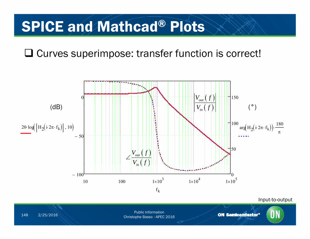
Curves superimpose: transfer function is correct!
40100
(dB) (°)
20 020 logH1 i 2 fk
1V10
arg H1 i 2 fk 180
outV fD f
outV fD f
(dB) (°)
0100
D f
10 100 1 103 1 104 1 105
fk
Public InformationChristophe Basso –APEC 2016143 2/25/2016
Control-to-output
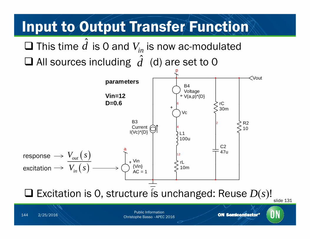
Input to Output Transfer Function Thi ti i 0 d V i d l t dd This time is 0 and Vin is now ac-modulated All sources including (d) are set to 0
d
pd
rC
Voutparameters
Vin=12D=0.6 6
B4VoltageV(a,p)*D
4
L1
2
rC30m
R210
D 0.6
B3Current
I(Vc)*D
Vc
12
L1100u
C247u
VinVi
rL
a
outV sV
responseVinAC = 1
10m inV sexcitation
Excitation is 0 structure is unchanged: Reuse D(s)!Public Information
Christophe Basso –APEC 2016144 2/25/2016
Excitation is 0, structure is unchanged: Reuse D(s)!slide 131
Static Gain - Response for s = 0
Open the capacitor and short the inductor2Ip
V 0 0iV V D V D
1I 0, outV a V D
outV
r
0 0out in outC
L
V V D V DI
r
0 01 0
out in out
L
V V D V DI D
r
I0CI D
Cr
loadR
Lr 1out C loadV I I R
Solve for VoutCI
2CrV
a
Solve for Voutand rearrange
1 loadout D D RV DH
LrinV 0 2
011
loadout
in s load L
V DHV DD R r
Public InformationChristophe Basso –APEC 2016145 2/25/2016
Input-to-output
Determining the Numerator: Null Vout To determine zeros bring the excitation back To determine zeros, bring the excitation back
“What conditions in the transformed circuit
0 ˆ 0outv
1Iˆ 0outi
Cr
0in outV s V s D transformed circuit null the response?”
ˆ 0i Excitation
0CI DCI
C
loadR ˆ 0outv 1
0outi
11sL
1sC
12
1 0CZ s rsC
What if L1 is set to its HF state?
12
1z
Cr C
Lr
2sC
1Z s
What if L1 is set to its HF state?
0CI 0 0CI D
No response, 1 zero only
Public InformationChristophe Basso –APEC 2016146 2/25/2016
p yInput-to-output
Final Transfer Function
1V s sr CD
The transfer function is immediated
600mV
22
0 0
11
1
out C
in
V s sr CDV s D s s
Q
parameters
Vin=12D=0.6
da
PW
M s
witc
h V
M X1PWMCCMVM
22 4V1 0V
01 2
1 DL C
9
L1100u
8
rC30m
11VinVinAC = 1
Vout
c
Pp
V5D
d55.9mV
-22.4V15.0V
2
1
1 loadC
Q D RL
12 2
C247u
R210
rL10m
D-22.4V55.9mV
1
Large-signal PWM switch model
Public InformationChristophe Basso –APEC 2016147 2/25/2016
Input-to-output
SPICE and Mathcad® Plots
Curves superimpose: transfer function is correct!
0 150
outV f(dB) (°)
0
10020 log H2 i 2 fk 10 arg H2 i 2 fk 180
inV f(dB) (°)
50
50
out
in
V fV f
10 100 1 103 1 104 1 105100 0
fk
in f
Public InformationChristophe Basso –APEC 2016148 2/25/2016
Input-to-output
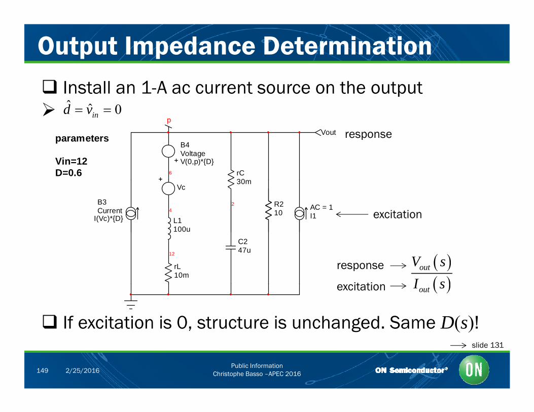
Output Impedance Determination Install an 1-A ac current source on the output ˆ ˆ 0ind v
p
rC30
Voutparameters
Vin=12D=0.6 6
B4VoltageV(0,p)*D
response
4
L1100u
2
30m
R210
AC = 1I1
B3Current
I(Vc)*D
Vc
excitation
12
C247u
rL10m
outV sI s
response
it ti outI sexcitation
If excitation is 0, structure is unchanged. Same D(s)!
Public InformationChristophe Basso –APEC 2016149 2/25/2016
slide 131
Static Resistance: Response for s = 0 Open the capacitor and short the inductor
VoutV 1V DV V D
outI
1I 2I 00, outV V D
outV
r
00 1outout outC
L L
V DV V DI
r r
01outV DI D
2
outVI
I0CI D
Cr
loadR
1 0L
I Dr
2
load
IR
outI 2 1out CI I I I
CI
2C
Factor Vout and rearrange
V rLr
0
201
out L
Lout
load
V rR
rI DR
Public InformationChristophe Basso –APEC 2016150 2/25/2016
Output impedance
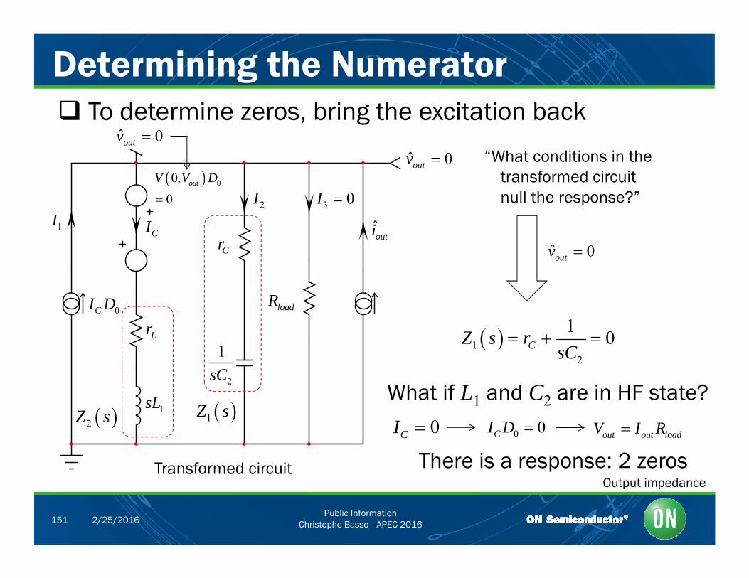
Determining the Numerator To determine zeros bring the excitation back To determine zeros, bring the excitation back
ˆ 0outv “What conditions in the transformed circuit 0V V D
ˆ 0outv
transformed circuit null the response?”
ˆ 0v Cr
00,0
outV V D
1ICI
2I 3 0I
outi
1
0outv
loadR
C
0CI D
12
1 0CZ s rsC
What if L1 and C2 are in HF state?2
1sC
Lr
L What if L1 and C2 are in HF state?
0CI 0 0CI D
There is a response: 2 zeros
1sL
out out loadV I R 1Z s 2Z s
Transformed circuit
Public InformationChristophe Basso –APEC 2016151 2/25/2016
pTransformed circuitOutput impedance
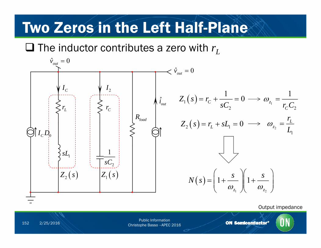
Two Zeros in the Left Half-Plane The inductor contributes a zero with The inductor contributes a zero with rL
ˆ 0outv ˆ 0outv
CrLr
CI 2I
outi 12
1 0CZ s rsC
1
2
1z
Cr C
loadRCrLr
0CI D
2 2C
2 1 0LZ s r sL 2
1
Lz
rL
2
1sC
1sL
1Z s 2Z s 1 2
1 1z z
s sN s
Public InformationChristophe Basso –APEC 2016152 2/25/2016
Output impedance
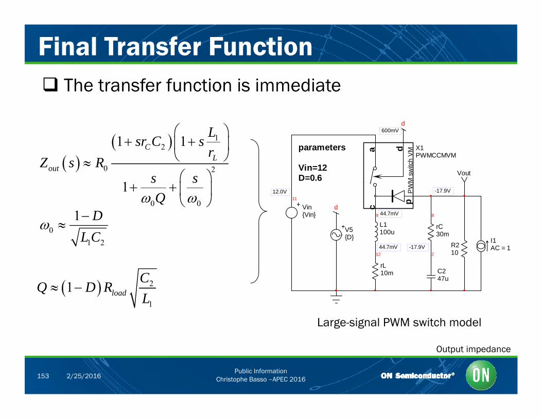
Final Transfer Function
L
The transfer function is immediate
d600mV
1
2
0 2
1 1
1
CL
out
Lsr C sr
Z s Rs s
Vout
parameters
Vin=12D=0.6
da
M s
witc
h V
M X1PWMCCMVM
600mV
0 0
1 s sQ
01 D
L C
9
L1100u
8
rC30m
11
VinVin
c
PW
p
V5D
d44.7mV
-17.9V12.0V
1 2L C
21C
Q D R
12 2
30m
C247u
R210
rL10m
I1AC = 1
D-17.9V44.7mV
1
1 loadQ D RL
Large-signal PWM switch model
Public InformationChristophe Basso –APEC 2016153 2/25/2016
Output impedance
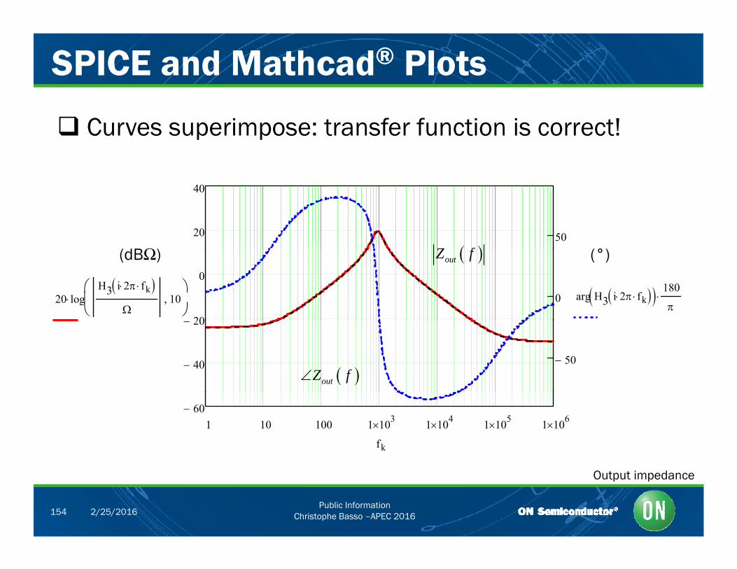
SPICE and Mathcad® Plots
Curves superimpose: transfer function is correct!
20
40
50 Z f(dBΩ) (°)
20
0
020 logH3 i 2 fk
10
arg H3 i 2 fk 180
outZ f(dBΩ) (°)
40
20
50 outZ f
1 10 100 1 103 1 104 1 105 1 10660
fk
Public InformationChristophe Basso –APEC 2016154 2/25/2016
Output impedance
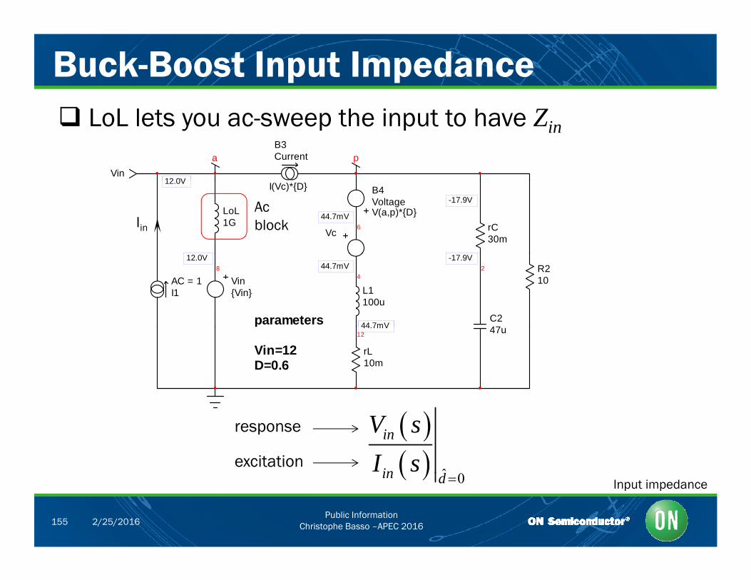
Buck-Boost Input Impedance
Vin
B3Currenta p
12 0V
LoL lets you ac-sweep the input to have Zin
rC30m
LoL1G
I(Vc)*D
6
B4VoltageV(a,p)*D
Vc
-17.9V
12.0V
44.7mVAc blockIin
4
L1100u
2
C247
R210
8
VinVin
parameters
AC = 1I1
44.7mV
44 7mV
-17.9V12.0V
12 47up
Vin=12D=0.6
rL10m
44.7mV
ˆ
in
in d
V sI s
response
excitation
Public InformationChristophe Basso –APEC 2016155 2/25/2016
0in d Input impedance
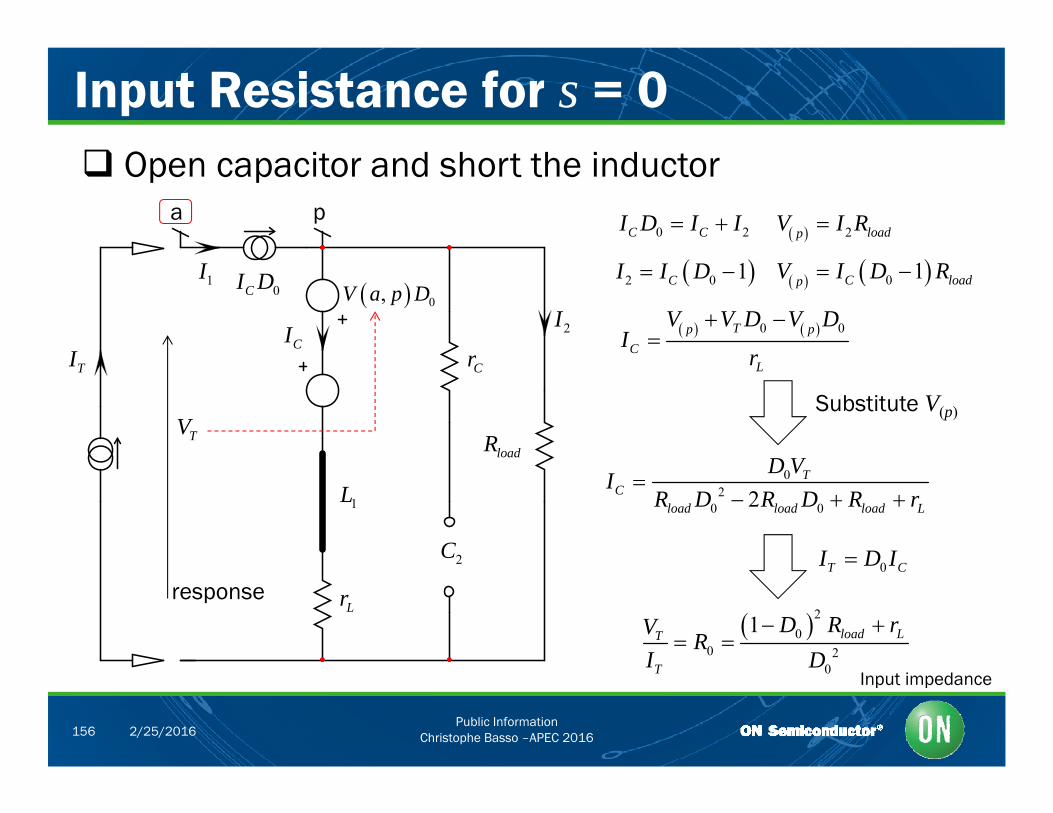
Input Resistance for s = 0 Open capacitor and short the inductor
a p0 2C CI D I I 2 loadpV I R
CII
1I
2I 0,V a p D0CI D
0 0Tp pC
V V D V DI
r
0 1C loadpV I D R 2 0 1CI I D
loadR
CrTI
TV
Lr
D V
Substitute V(p)
1L
2C
02
0 02T
Cload load load L
D VI
R D R D R r
I D Iresponse
Lr
2 0T CI D I
20
0 2
1 load LT D R rVR
I D
Public InformationChristophe Basso –APEC 2016156 2/25/2016
0TI DInput impedance
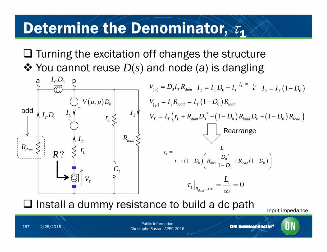
Determine the Denominator, 1
Turning the excitation off changes the structure You cannot reuse D(s) and node (a) is dangling
I Da p
I I 0,V a p D
0CI D 0 T dumaV D I R 2 0C TI I D I 2 01TI I D C TI I
2 01load T loadpV I R I D R add
CrCI 2I
0CI D
loadRTI
20 0 0 01 1T T L dum load loadV I r R D D R D D R
Rearrange
add
LrdumR
2C
?RT
1
1 20
0 00
1 11L dum load
LDr D R R D
D
TV
Install a dummy resistance to build a dc path
11 0
dumR
L
Public InformationChristophe Basso –APEC 2016157 2/25/2016
Install a dummy resistance to build a dc pathInput impedance
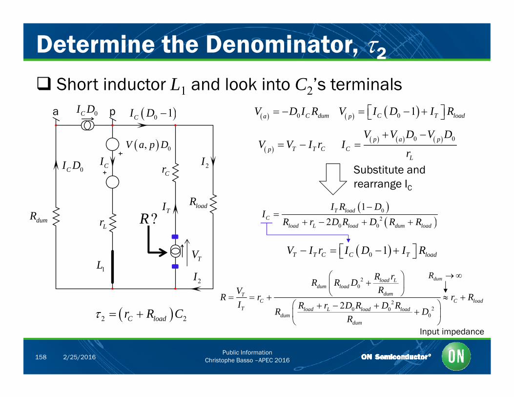
Determine the Denominator, 2
a p0CI D
Short inductor L1 and look into C2’s terminals
0 1C T loadpV I D I R 0 1CI D 0 C dumaV D I R
CrCI 2I
0,V a p D
0CI D
0 0p a pC
L
V V D V DI
r
T T CpV V I r
Substitute and C
loadR
rdumR ?RTI
Subst tute a drearrange IC
02
12
T loadC
l d l d d l d
I R DI
R r D R D R R
Lr ?
TV1L
0 02load L load dum loadR r D R D R R
0 1T T C C T loadV I r I D I R
R RI 20
220 0
02
load Ldum load
dumTC C load
T load L load loaddum
dum
R rR R DRV
R r r RI R r D R D RR D
R
2 2C loadr R C
dumR 2I
Public InformationChristophe Basso –APEC 2016158 2/25/2016
dum Input impedance
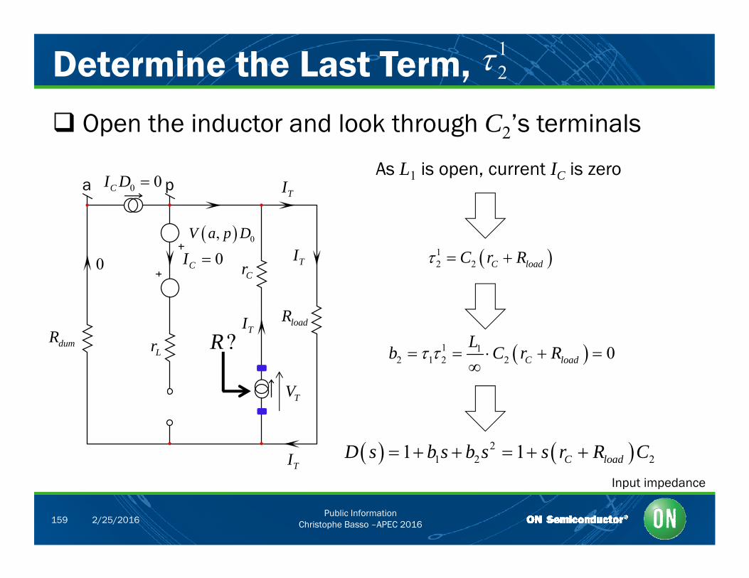
Determine the Last Term, 12
Open the inductor and look through C2’s terminals
0I DAs L1 is open, current IC is zero
a p
0,V a p D
0 0CI D TI
I 1 C RCr
0CI 0
loadRI
TI 12 2 C loadC r R
LrdumR ?R
TV
TI
1 12 1 2 2 0C load
Lb C r R
T
TI 21 2 21 1 C loadD s b s b s s r R C
Public InformationChristophe Basso –APEC 2016159 2/25/2016
Input impedance
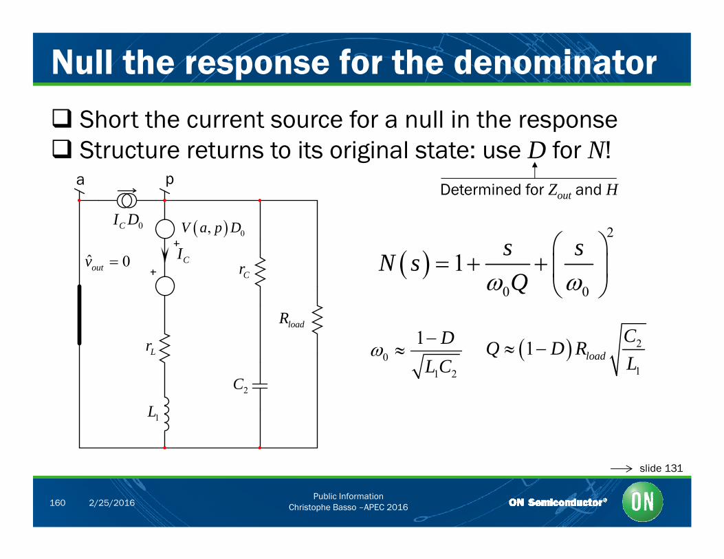
Null the response for the denominator Short the current source for a null in the response Structure returns to its original state: use D for N!
Determined for Zout and Ha p
0,V a p D0CI D2
s s Cr
R
ˆ 0outv CI 0 0
1 s sN sQ
loadR
Lr
C
01 2
1 DL C
2
1
1 loadC
Q D RL
2C
1L
Public InformationChristophe Basso –APEC 2016160 2/25/2016
slide 131
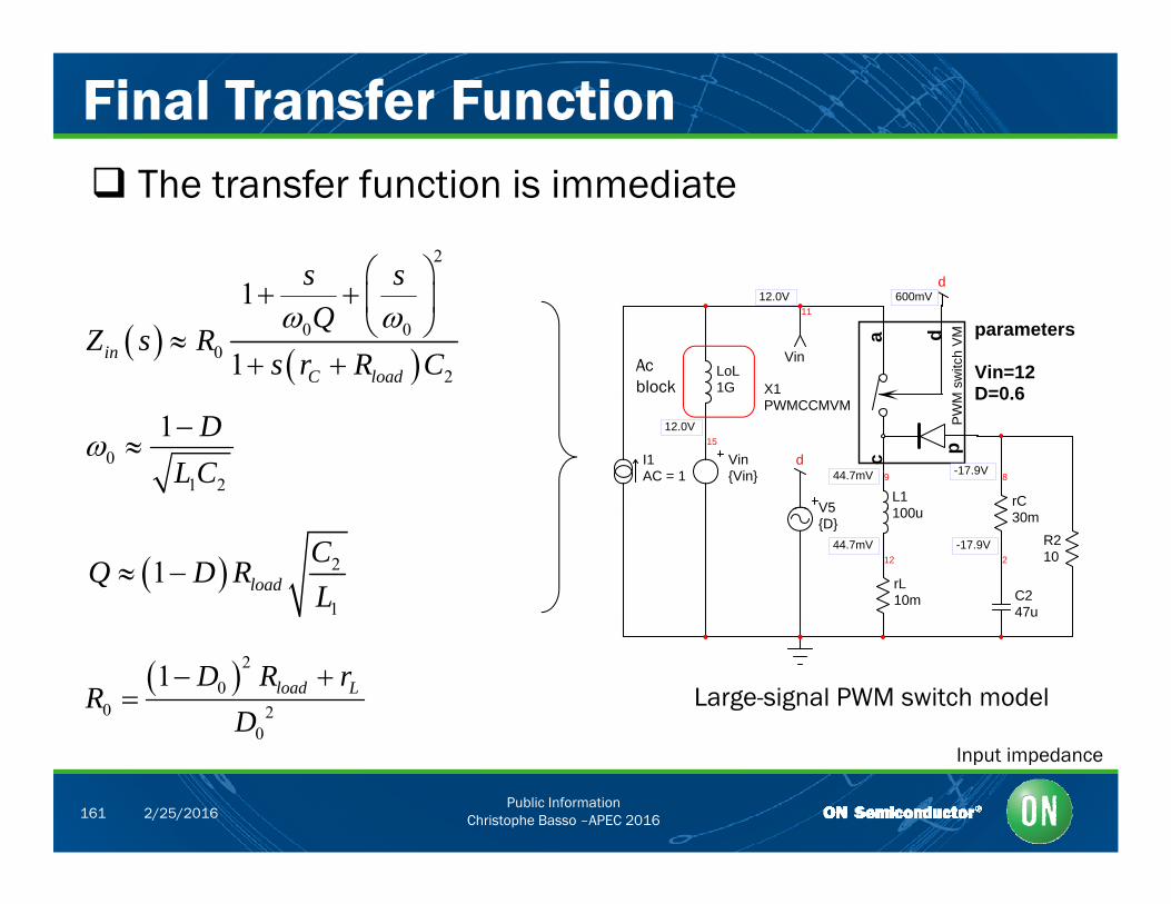
Final Transfer Function
2s s
The transfer function is immediate
d
0 0
02
1
1inC load
s sQ
Z s Rs r R C
11
Vin
parameters
Vin=12D=0 6
LoL1G
da
M s
witc
h V
M
X1
d12.0V 600mV
Ac block
01 2
1 DL C
9
L1100
8
rC
15
VinVin
D=0.6
I1AC = 1
c
PW
Mp
PWMCCMVM
V5
d44.7mV -17.9V
12.0V
2
1
1 loadC
Q D RL
12
100u
2
30m
C247u
R210
rL10m
V5D
44.7mV -17.9V
Large-signal PWM switch model 2
00 2
0
1 load LD R rR
D
Public InformationChristophe Basso –APEC 2016161 2/25/2016
0Input impedance
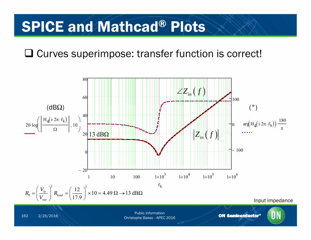
SPICE and Mathcad® Plots
Curves superimpose: transfer function is correct!
60
80
100
(dBΩ) (°)
inZ f
20
40
020 logH4 i 2 fk
10
arg H4 i 2 fk 180
(dBΩ) (°)
Z f13 dBΩ
0
20
100
inZ f13 dBΩ
1 10 100 1 103 1 104 1 105 1 10620
fk2 2
012 10 4.49 Ω 13 dBΩ
17 9in
loadV
R RV
Public InformationChristophe Basso –APEC 2016162 2/25/2016
0 17.9loadoutV
Input impedance
References
Middlebrook R.D. “Null Double Injection and The Extra Element Theorem”, IEEE Transactions on Education, Vol. 32, , , ,NO 3, August 1989 R. D. Middlebrook, V. Vorpérian, J. Lindal, “The N Extra Element Theorem” IEEE Transactions on Circuits and Element Theorem , IEEE Transactions on Circuits and Systems, vol. 45, NO. 9, September 1998 V. Vorpérian, “Fast Analytical Techniques for Electrical and
C C 9 8 0Electronic Circuits”, Cambridge University Press, 978-0-52162-442-8, 2002 C. Basso, “Linear Circuit Transfer Functions: A Tutorial Introduction to Fast Analytical Techniques”, Wiley IEEE-press, May 2016
Public InformationChristophe Basso –APEC 2016163 2/25/2016
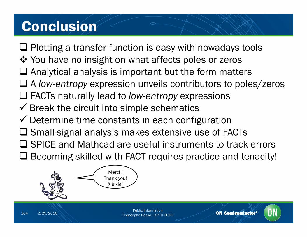
Conclusion Plotting a transfer function is easy with nowadays tools You have no insight on what affects poles or zeros Analytical analysis is important but the form matters Analytical analysis is important but the form matters A low-entropy expression unveils contributors to poles/zeros FACTs naturally lead to low-entropy expressions Break the circuit into simple schematics Determine time constants in each configuration Small-signal analysis makes extensive use of FACTs Small signal analysis makes extensive use of FACTs SPICE and Mathcad are useful instruments to track errors Becoming skilled with FACT requires practice and tenacity!
Merci !Thank you!
Xiè-xie!
Public InformationChristophe Basso –APEC 2016164 2/25/2016