Embed Size (px)
Citation preview
1
Introduction to Radiation-Resistant SemiconductorDevices and Circuits
Helmuth Spieler
Ernest Orlando Lawrence Berkeley National Laboratory, Physics Division,1 Cyclotron Road, Berkeley, CA 94720, USA
Abstract
This tutorial paper provides an overview of design considerations forsemiconductor radiation detectors and electronics in high radiation environments.Problems specific to particle accelerator applications are emphasized and many ofthe presented results originated in extensive studies of radiation effects in largescale particle detectors for the SSC and LHC. Basic radiation damage mechanismsin semiconductor devices are described and specifically linked to electronicparameter changes in detectors, transistors and integrated circuits. Mitigationtechniques are discussed and examples presented to illustrate how the choice ofsystem architecture, circuit topology and device technology can extend the range ofoperation to particle fluences >1014 cm-2 and ionizing doses >100 Mrad.
INTRODUCTION
Radiation-resistant electronics have been integral to the aerospace, nuclearreactor and weapons communities for many years, but only rather recently havethey become important for particle accelerators and accelerator-based experiments.The SSC made the design of radiation-resistant detectors and electronic read-outsystems a key design consideration for high-energy physics experimentalists. Theenergy frontier has now shifted to the LHC, which requires even higher luminosi-ties to achieve its physics goals. Even at existing machines, for example theTevatron at FNAL, radiation-hard electronics are required in the innermosttracking systems. The vertex detector for BaBar at the SLAC B-Factory requiresradiation-hard electronics. On the accelerator side, higher beam currents and theincreased sophistication of monitoring and diagnostic systems are bringing theneed for radiation-resistant electronics to the forefront of designers’ concerns.
Although one can argue that vacuum tubes are extremely radiation hard, thecomplexity of today’s electronics systems restricts our focus to semiconductordevices. For all practical purposes this leaves us with silicon and gallium-arsenidedevices. For a variety of reasons silicon transistors and integrated circuits comprisethe bulk of radiation-hard electronics. In designing SSC and LHC detectors, wehave found no compelling justification for GaAs electronics in any radiation-sensitive application. Indeed, in some areas silicon technology provides critical
2
performance advantages. For these reasons, despite the fascinating physics ofcompound semiconductors, this tutorial will emphasize silicon technology.
The study of radiation effects in semiconductor electronics and the develop-ment of radiation-resistant integrated circuits have formed an active scientificcommunity that has produced a wealth of data and conceptual understanding.Although access to some of these results and techniques is restricted, most of thedata and papers are in the public domain and readily accessible, and they provide avaluable resource (see the Bibliography at the end of this paper). Although, muchhas been published on basic damage mechanisms and on device properties forspecific applications, when attempting to apply this information to an area outsidethe traditional purview of the radiation effects community, key pieces ofinformation needed to link basic damage mechanisms to usable design guidelinesare often missing. This was very clear in the development of detectors for the SSCand LHC, where both the application of detectors with deep depletion regions andnovel circuit designs combining low-noise, high-speed and low power pusheddevelopments into uncharted territory.
This is a very complicated field and developing a general road map is not easy,but one can apply a few fundamental considerations to understanding the effects ofradiation on device types in specific circuit topologies and narrow the range ofoptions that must be studied in detail. That is the thrust of this tutorial. For lack oftime, some treatments are sketchier than desirable and the reader should consultthe references and the bibliography. This paper originated as a tutorial talk at the1996 Beam Instrumentation Workshop at Argonne National Laboratory in May,1996 and will be expanded and modified in response to criticisms and newdevelopments. (1)
RADIATION DAMAGE MECHANISMS
Semiconductor devices are affected by two basic radiation damagemechanisms:
• Displacement damage: Incident radiation displaces silicon atoms from theirlattice sites. The resulting defects alter the electronic characteristics of thecrystal.
• Ionization damage: Energy absorbed by electronic ionization in insulatinglayers, predominantly SiO2, liberates charge carriers, which diffuse or drift toother locations where they are trapped, leading to unintended concentrations ofcharge and, as a consequence, parasitic fields.
3
Both mechanisms are important in detectors, transistors and integrated circuits.Some devices are more sensitive to ionization effects, some are dominated bydisplacement damage. Hardly a system is immune to either one phenomena andmost are sensitive to both.
Ionization effects depend primarily on the absorbed energy, independent of thetype of radiation. At typical incident energies ionization is the dominant absorptionmechanism, so that ionization damage can be measured in terms of energy absorp-tion per unit volume, usually expressed in rad or gray (1 rad= 100 erg/g, 1 Gy= 1J/kg= 100 rad). Since the charge liberated by a given dose depends on the absorbermaterial, the ionizing dose must be referred to a specific absorber, for example1 rad(Si), 1 rad(SiO2), 1 rad(GaAs), or in SI units 1 Gy(Si), etc.
Displacement damage depends on the non-ionizing energy loss, i.e. energy andmomentum transfer to lattice atoms, which depends on the mass and energy of theincident quanta. A simple measure as for ionizing radiation is not possible, so thatdisplacement damage must be specified for a specific particle type and energy.
In general, radiation effects must be measured for both damage mechanisms,although one may choose to combine both, for example by using protons, if onehas sufficient understanding to unravel the effects of the two mechanisms by elec-trical measurements. Even non-ionizing particles can deposit some ionization dosevia recoils, but this contribution tends to be very small: 2⋅10-13 rad per 1 MeVneutron/cm2, for example. (2)
To set the scale, consider a tracking detector operating at the LHC with aluminosity of 1034 cm-2s-1. In the innermost volume of a tracker the particle fluxfrom collisions is n’≈ 2⋅109/r⊥
2 cm-2s-1, increasing roughly twofold in the outerlayers due to interactions and loopers. At r⊥=30 cm the particle fluence after oneyear of operation (107 s) is about 2⋅1013 cm-2. A fluence of 3⋅1013 cm-2 of minimumionizing particles corresponds to an ionization dose of 1 Mrad, obtained after 1.5years of operation. Albedo neutrons from a calorimeter could add a yearly fluenceof 1012 to 1013 cm-2.
Displacement Damage
An incident particle or photon capable of imparting an energy of about 20 eVto a silicon atom can dislodge it from its lattice site. Displacement damage createsdefect clusters. For example, a 1 MeV neutron transfers about 60 to 70 keV to theSi recoil atom, which in turn displaces roughly 1000 additional atoms in a region ofabout 0.1 µm size. Displacement damage is proportional to non-ionizing energyloss (3), which is not proportional to the total energy absorbed, but depends on theparticle type and energy. Non-ionizing energy loss for a variety of particles has
4
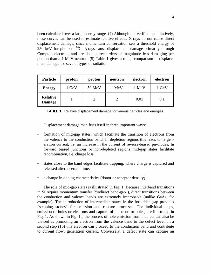
been calculated over a large energy range. (4) Although not verified quantitatively,these curves can be used to estimate relative effects. X-rays do not cause directdisplacement damage, since momentum conservation sets a threshold energy of250 keV for photons. 60Co γ rays cause displacement damage primarily throughCompton electrons and are about three orders of magnitude less damaging perphoton than a 1 MeV neutron. (5) Table 1 gives a rough comparison of displace-ment damage for several types of radiation.
Displacement damage manifests itself in three important ways:
• formation of mid-gap states, which facilitate the transition of electrons fromthe valence to the conduction band. In depletion regions this leads to a gen-eration current, i.e. an increase in the current of reverse-biased pn-diodes. Inforward biased junctions or non-depleted regions mid-gap states facilitaterecombination, i.e. charge loss.
• states close to the band edges facilitate trapping, where charge is captured andreleased after a certain time.
• a change in doping characteristics (donor or acceptor density).
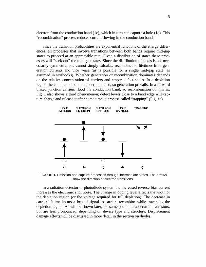
The role of mid-gap states is illustrated in Fig. 1. Because interband transitionsin Si require momentum transfer (“indirect band-gap”), direct transitions betweenthe conduction and valence bands are extremely improbable (unlike GaAs, forexample). The introduction of intermediate states in the forbidden gap provides“stepping stones” for emission and capture processes. The individual steps,emission of holes or electrons and capture of electrons or holes, are illustrated inFig. 1. As shown in Fig. 1a, the process of hole emission from a defect can also beviewed as promoting an electron from the valence band to the defect level. In asecond step (1b) this electron can proceed to the conduction band and contributeto current flow, generation current. Conversely, a defect state can capture an
Particle proton proton neutron electron electron
Energy 1 GeV 50 MeV 1 MeV 1 MeV 1 GeV
RelativeDamage
1 2 2 0.01 0.1
TABLE 1. Relative displacement damage for various particles and energies.
5
electron from the conduction band (1c), which in turn can capture a hole (1d). This“recombination” process reduces current flowing in the conduction band.
Since the transition probabilities are exponential functions of the energy differ-ences, all processes that involve transitions between both bands require mid-gapstates to proceed at an appreciable rate. Given a distribution of states these proc-esses will “seek out” the mid-gap states. Since the distribution of states is not nec-essarily symmetric, one cannot simply calculate recombination lifetimes from gen-eration currents and vice versa (as is possible for a single mid-gap state, asassumed in textbooks). Whether generation or recombination dominates dependson the relative concentration of carriers and empty defect states. In a depletionregion the conduction band is underpopulated, so generation prevails. In a forwardbiased junction carriers flood the conduction band, so recombination dominates.Fig. 1 also shows a third phenomenon; defect levels close to a band edge will cap-ture charge and release it after some time, a process called “trapping” (Fig. 1e).
FIGURE 1. Emission and capture processes through intermediate states. The arrowsshow the direction of electron transitions.
In a radiation detector or photodiode system the increased reverse-bias currentincreases the electronic shot noise. The change in doping level affects the width ofthe depletion region (or the voltage required for full depletion). The decrease incarrier lifetime incurs a loss of signal as carriers recombine while traversing thedepletion region. As will be shown later, the same phenomena occur in transistors,but are less pronounced, depending on device type and structure. Displacementdamage effects will be discussed in more detail in the section on diodes.
6
Ionization Damage
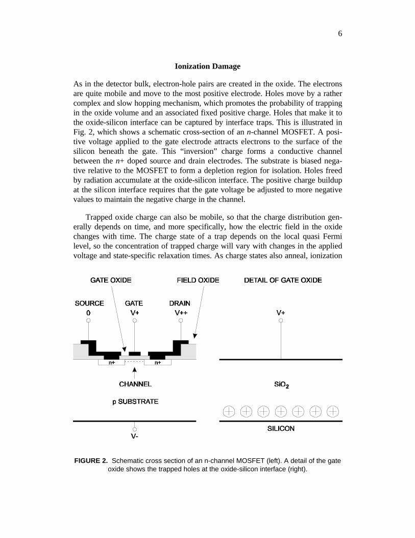
As in the detector bulk, electron-hole pairs are created in the oxide. The electronsare quite mobile and move to the most positive electrode. Holes move by a rathercomplex and slow hopping mechanism, which promotes the probability of trappingin the oxide volume and an associated fixed positive charge. Holes that make it tothe oxide-silicon interface can be captured by interface traps. This is illustrated inFig. 2, which shows a schematic cross-section of an n-channel MOSFET. A posi-tive voltage applied to the gate electrode attracts electrons to the surface of thesilicon beneath the gate. This “inversion” charge forms a conductive channelbetween the n+ doped source and drain electrodes. The substrate is biased nega-tive relative to the MOSFET to form a depletion region for isolation. Holes freedby radiation accumulate at the oxide-silicon interface. The positive charge buildupat the silicon interface requires that the gate voltage be adjusted to more negativevalues to maintain the negative charge in the channel.
Trapped oxide charge can also be mobile, so that the charge distribution gen-erally depends on time, and more specifically, how the electric field in the oxidechanges with time. The charge state of a trap depends on the local quasi Fermilevel, so the concentration of trapped charge will vary with changes in the appliedvoltage and state-specific relaxation times. As charge states also anneal, ionization
FIGURE 2. Schematic cross section of an n-channel MOSFET (left). A detail of the gateoxide shows the trapped holes at the oxide-silicon interface (right).

7
effects depend not only on the dose, but also on the dose rate. Fig. 2 also shows athick field oxide, which serves to control the silicon surface charge adjacent to theFET and prevent parasitic channels to adjacent devices. The same positive chargebuildup as in the gate oxide also occurs here, indeed it can be exacerbated becausethe field oxide is quite thick. For more details, see ref. (6), currently theauthoritative text on ionization effects.
In summary, ionization effects are determined by
• Interface trapped charge
• Oxide trapped charge
• The mobility of trapped charge
• The time and voltage dependence of charge states
Although the primary radiation damage depends only on the absorbed ionizingenergy, the resulting effects of this dose depend on the rate of irradiation, theapplied voltages and their time variation, the temperature, and the time variation ofthe radiation itself. Ionization damage manifests itself most clearly in MOS fieldeffect transistors, so it will be discussed in more detail in that section.
EFFECTS ON DEVICE CHARACTERISTICS
Radiation Damage in Diodes
Diode structures are basic components of more complex devices, for examplebipolar transistors, junction FETs and integrated circuits. Since the properties ofdiode depletion regions are determined primarily by bulk properties, measurementson diodes will serve to illustrate the effects of displacement damage. Reversebiased diodes with large depletion depths are used as radiation detectors andphotodiodes. Because of their large depletion depths, typically hundreds ofmicrons, detector diodes are very sensitive to bulk damage and extensive work bythe SSC/LHC community has produced many insights into bulk radiation effects.Affected are the detector leakage current, the doping characteristics, and chargecollection.
A theoretical analysis from first principles is quite complex, due to the manyphenomena involved. Take doping changes as an example. Si interstitials are quiteactive and displace either P donors or B acceptors from substitutional sites andrender them electrically inactive. These interstitial dopants together with oxygen,
8
commonly present in the lattice as an impurity, react in very different ways withvacancies to form complexes with a variety of electronic characteristics (see ref.(7) and references therein). Fortuitously, although a multitude of competing effectscan be invoked in to predict and interpret experimental results, the data can bedescribed by rather simple parametrizations.
The increase in reverse bias current (leakage current) is linked to the creationof mid-gap states. Experimental data are consistent with a uniform distribution ofactive defects in the detector volume. The bias current after irradiation
I I Addet = + ⋅ ⋅0 α Φ (1)
where I0 is the bias current before irradiation, α is a damage coefficient dependenton particle type and fluence, Φ is the particle fluence, and the product of detectorarea and thickness Ad is the detector volume. For 650 MeV protons α≈3⋅10-17 A/cm (8,9) and for 1 MeV neutrons (characteristic of the albedo emanatingfrom a calorimeter) α≈ 2⋅10-17 A/cm. (9) The parametrization used in Eq. 1 is quitegeneral, as it merely assumes a spatially uniform formation of electrically activedefects in the detector volume, without depending on the details of energy levelsor states.
The coefficients given above apply to room temperature operation. The reversebias current of silicon detectors depends strongly on temperature
I T T eRE k TB( ) /∝ − 2 2 (2)
if the generation current dominates (10), as is the case for substantial radiationdamage. The effective activation energy E= 1.2 eV for radiation damaged samples(8)(11)(12), whereas unirradiated samples usually exhibit E= 1.15 eV. The ratio ofcurrents at two temperatures T1 and T2 is
−−
=
21
212
1
2
1
22
exp )(
)(
TT
TT
k
E
T
T
TI
TI
BR
R (3)
After irradiation the leakage current initially decreases with time. Pronouncedshort term and long term annealing components are observed and precise fits to theannealing curve require a sum of exponentials. (9) Experimentally, decreases byfactors of 2 to 3 have been observed with no further improvement after 5 monthsor so. (8,5) In practice, the variation of leakage current with temperature is veryreproducible from device to device, even after substantial doping changes due toradiation damage. The leakage current can be used for dosimetry and diodes areoffered commercially specifically for this purpose.

9
The effect of displacement damage on doping characteristics has beeninvestigated in the course of detector studies for the SSC and LHC and is still thesubject of ongoing study. Measurements on a variety of strip detectors and photo-diodes by groups in the U.S., Japan and Europe have shown that the effectivedoping of n type silicon initially decreases, becomes intrinsic (i.e. very little spacecharge) and then turns p-like, with the space charge increasing with fluence. Thisphenomenon is consistent with the notion that acceptor sites are formed by theirradiation, although this does not mean that mobile holes are created. (13)Initially, the effective doping level Nd -Na decreases as new acceptor statesneutralize original donor states. At some fluence the two balance, creating“intrinsic” material, and beyond this fluence the acceptor states dominate. Inaddition, there is evidence for a concurrent process of donor removal. (14,15)Since the probability of donor removal is proportional to the initial donorconcentration Nd0, whereas the formation of defects leading to acceptor states isproportional to fluence, the effective space charge density Neff of n type startingmaterial after exposure to a particle fluence Φ is described by (16)
N N e g g e N t Teff dc
c st T
Y( ) ( , , )/ ( )Φ Φ Φ ΦΦ= − + + ⋅ +− − 0τ (4)
where a negative or positive sign of Neff denotes whether the effective space chargeis n- or p-like. The first term describes the removal of donors and the second thecreation of acceptors. c and gc are constants for a given particle type and energythat describe the stable component of radiation damage. The third and fourth termsdescribe the time and temperature dependent changes in the effective doping con-centration and will be discussed later. For high energy protons the average frommany measurements is c= (0.96±0.19)⋅10-13 cm2 and gc = (1.15±0.09)⋅10-2 cm-1.Type inversion from n to p type silicon occurs at a fluence of about 1013 cm-2. Datafor 1 MeV equivalent neutrons yield c= (2.29±0.63)⋅10-13 cm2 andgc = (1.77±0.07)⋅10-2 cm-1. (9)
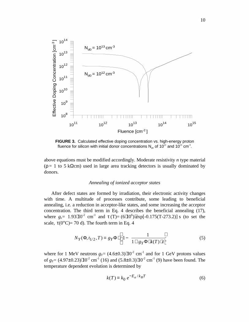
After a proton fluence Φ= 1014 cm-2 the acceptor concentration before anneal-ing is 1012 cm-3, which requires a bias voltage of 165V for full depletion of a 300µm thick detector. At first glance, it would seem that beginning with a highern doping level Nd0 (lower resistivity) would increase overall detector lifetime.Although the inversion fluence increases with larger values of Nd0 , the difference indoping concentration is negligible at larger fluences since the exponential termquickly becomes insignificant. (15) For example, as shown in Fig. 3 materials withinitial doping densities of 1012 cm-3 and 1013 cm-3 lie within 15% at Φ= 5⋅1013 cm-2.
Very high resistivity silicon (ρ >10 kΩcm or Nd < 4⋅1011 cm-3) is often highlycompensated, Neff=Nd -Na with Nd ~Na>>Neff , so that minute changes to eitherdonors or acceptors can alter the net doping concentration significantly, and the
10
above equations must be modified accordingly. Moderate resistivity n type material(ρ = 1 to 5 kΩcm) used in large area tracking detectors is usually dominated bydonors.
Annealing of ionized acceptor states
After defect states are formed by irradiation, their electronic activity changeswith time. A multitude of processes contribute, some leading to beneficialannealing, i.e. a reduction in acceptor-like states, and some increasing the acceptorconcentration. The third term in Eq. 4 describes the beneficial annealing (17),where gs= 1.93⋅10-2 cm-1 and τ (T)= (6⋅106)⋅exp[-0.175(T-273.2)] s (to set thescale, τ(0°C)= 70 d). The fourth term in Eq. 4
N t T gg k T tY Y
Y( , , )
( )Φ Φ
Φ1/2 11
1= ⋅ −
+ ⋅ ⋅
(5)
where for 1 MeV neutrons gY= (4.6±0.3)⋅10-2 cm-1 and for 1 GeV protons valuesof gY= (4.97±0.23)⋅10-2 cm-1 (16) and (5.8±0.3)⋅10-2 cm-1 (9) have been found. Thetemperature dependent evolution is determined by
k T k e E k Ta B( ) /= −0 (6)
1011 1012 1013 1014 1015
Fluence [cm-2 ]
108
109
1010
1011
1012
1013
1014
Effe
ctiv
e D
opin
g C
once
ntra
tion
[cm
-3 ]
Nd0 = 1013 cm-3
Nd0 = 1012 cm-3
FIGURE 3. Calculated effective doping concentration vs. high-energy protonfluence for silicon with initial donor concentrations Nd0 of 1012 and 1013 cm-3.
11
Typical parameter sets are k0 = (0.85+25-0.82) cm3/s and Ea= 1.16±0.08 eV (16),and k0 = (520+1590-392) cm3/s and Ea= 1.31±0.04 eV (9).
Anti-annealing is a concern because of its effect on detector depletion voltage,i.e. the voltage required to collect mobile charge from the complete thickness ofthe silicon detector. Since this voltage increases with space-charge concentration,antiannealing can easily exceed the safe operating range, especially at highfluences. The relative effect of anti-annealing increases strongly with fluence andtemperature, as illustrated in Table 2, which shows the relative increase in dopingand required operating voltage. Clearly, low temperature operation is beneficial.Nevertheless, even a low temperature system will require maintenance at roomtemperature and warm up periods must be controlled very carefully. (9,16)
Data on charge collection efficiency are still rather sketchy. The primarymechanism is expected to be trapping of signal charge at defect sites, i.e. adecrease in carrier lifetime τ. Since the loss in signal charge is proportional toexp(-tc /τ ), reducing the collection time mitigates the effect. Since either theoperating voltage is increased or depletion widths are reduced at damage levelswhere charge trapping is appreciable, fields tend to be higher and collection timesdecrease automatically with radiation damage, provided the detector can sustainthe higher fields.
Typical measurements have determined the signal charge vs. bias voltage andhave taken the plateau value (or the maximum signal charge just below break-down). Lemeilleur et al. (18) find ∆Q/Q0 = γΦ, where γ = (0.024±0.004)⋅10-13 cm2
for 1 MeV equivalent neutrons. Fretwurst et al. (19) find similar results, with adependence 1/τ = γΦ, where for holes γp= 2.7⋅10-7 cm2s and for electronsγe= 1.2⋅10-6 cm2s for Φ>1013 cm-2 of 1 MeV equivalent neutrons. For a fluenceΦ= 5⋅1013 cm-2s-1, a 400 µm thick detector with a depletion voltage of 130Voperated at a bias voltage of 200V would show a decrease in signal charge of12%. Ohsugi et al. (20) have demonstrated the operation of strip detectors toneutron fluences beyond 1014 cm-2, with signal losses of about 10%. Similar results
Na (t=100h)/Na(t=0) = V (t=100h)/V (t=0)Fluence [cm-2]
0 °C 20 °C 40 °C
1013 1.00 1.02 1.39
1014 1.01 1.21 4.71
TABLE 2. Relative antiannealing after 100 h vs. fluence and temperature

12
have been obtained on fully irradiated strip detectors read out by LHC compatibleelectronics. (21)
The basic detector is insensitive to ionization effects. In the bulk, ionizingradiation creates electrons and holes that are swept from the sensitive volume;charge can flow freely through the external circuitry to restore equilibrium. Theproblem lies in the peripheral structures, the oxide layers that are essential to con-trolling leakage paths at the edge of the diode and to preserving inter-electrodeisolation in segmented detectors.
The positive space charge due to hole trapping in the oxide and at the interface(see Fig. 2) attracts electrons in the silicon bulk to the interface. These accumula-tion layers can exhibit high local electron densities and form conducting channels,for example between the detector electrodes. This is especially critical at the“ohmic” electrodes in double-sided detectors, where the absence of pn junctionsmakes operation rely on full depletion of the silicon surface (even without radia-tion, the silicon surface tends to be n-type, so the ohmic side of n type detectors isinherently more difficult to control). (22,23)
Some detectors include integrated coupling capacitors and biasing networks.Biasing structures such as punch-through resistors and MOSFET structures aresubject to ionization damage. Although these devices can remain functional, sub-stantial changes in voltage drop have been reported for punch-through and accu-mulation layer devices, whereas measurements on polysilicon resistors irradiated to4 Mrad (65 MeV p) show no effect. (24)
Radiation Damage in Transistors and Integrated Circuits
In principle, the same phenomena discussed for detectors also occur in transis-tors, except that the geometries of transistors are much smaller (depletion widths<1 µm) and the typical doping levels are higher (>1015 cm-3).
Bipolar Transistors
The most important damage mechanism in bipolar transistors is the degradationof DC current gain at low currents. The damage mechanism is the same that causesincreased leakage current in detectors, formation of mid-gap states by displace-ment damage. The difference is that the base-emitter junction is forward biased, sothe high carrier concentration in the conduction band tips the balance from genera-tion to recombination (see Fig. 1). The fractional carrier loss depends on therelative concentrations of injected carriers and defects. Consequently, thereduction of DC current gain due to radiation damage depends on current density.For a given collector current a small device will suffer less degradation in DCcurrent gain than a large one.
13
Since the probability of recombination depends on the transit time through thejunction region, reduced base width will also improve the radiation resistance.Base width is strongly linked with device speed, so that the reduction in DCcurrent gain βDC scales inversely with a transistor’s unity gain frequency fT . (25)
TDC f
Φ+=0
1
1
ββ (7)
Since IC technology is driven primarily by device speed, mainstream marketforces will indirectly improve the radiation resistance of bipolar transistor proc-esses. Mid-gap states also limit the low current performance before irradiation.Over the past decade, evolutionary improvements in contamination control andprocess technology have also yielded substantially better low-current performance.Measurements on bipolar transistors from several vendors have shown that proc-esses not specifically designed for radiation resistance are indeed quite usable insevere radiation environments, even at low currents. (26,27,28).
Changes in doping levels have little effect in bipolar transistors. Typical dopinglevels in the base and emitter are NB= 1018 and NE= 1020 cm-3. In the collectordepletion region doping levels are smaller, typically 1016, rising to 1018 or 1019 atthe collector contact. At these levels the change in doping level due to displace-ment damage (∆NA ≈ 1012 cm-3 at Φ= 1014 cm-2) is negligible, although local devicetemperatures may be high enough that anti-annealing leads to noticeable effects.
10-5
10-4
10-3
10-2
10-1
100
101
102
103
EMITTER CURRENT DENSITY [µA/(µm)2 ]
0
10
20
30
40
50
60
70
80
90
100
DC
CU
RR
EN
T G
AIN
PRE-RAD
POST RAD
10-5
10-4
10-3
10-2
10-1
100
101
102
103
EMITTER CURRENT DENSITY [µA/(µm)2 ]
0
10
20
30
40
50
DC
CU
RR
EN
T G
AIN
PRE-RAD
POST-RAD
NPN PNP
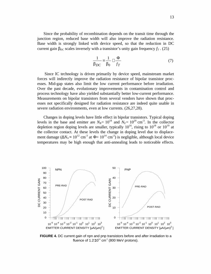
FIGURE 4. DC current gain of npn and pnp transistors before and after irradiation to afluence of 1.2⋅1014 cm-2 (800 MeV protons).

14
FIGURE 5. Noise of a bipolar transistor preamplifier before and after irradiation to afluence of 1.2⋅1014 cm-2 (800 MeV protons).
Figure 4 shows measured DC current gain for npn and pnp bipolar transistorsirradiated to a fluence of 1.2⋅1014 cm-2 (800 MeV protons). (26) These devices,fabricated in AT&T’s CBIC-V2 high-density complementary npn-pnp IC process,exhibit fT = 10 GHz for the npn and 4.5 GHz for the pnp transistors. In the CAFEchip designed for the ATLAS silicon tracker (29) the npn input device is operatedat a current density of about 2 µA/(µm)2, where the post-rad current gaindecreases to about 60% of its initial value. Although a smaller transistor woulddeteriorate less, the thermal noise contribution of the parasitic base resistancewould be excessive, so a compromise is necessary. No measurable changes intransconductance were measured, as expected. The output resistance of thesedevices decreased by <10% after irradiation. Similar results have been measuredon comparable devices fabricated by Maxim (Tektronix) (27,28) andWestinghouse. (30)
Noise degradation has been measured on individual transistors and completepreamplifier circuits. The results are consistent with the measured degradation inDC current gain and no change in transconductance or parasitic resistances, asexpected. Figure 5 shows the measured spectral noise density of a monolithicallyintegrated preamplifier before and after irradiation to 1.2⋅1014 cm-2 (800 MeVprotons). (26) The gain increased by a few percent after irradiation, so the inputnoise increase is somewhat smaller than shown.
1E+5 1E+6 1E+7 1E+8
FREQUENCY [Hz]
0.00
0.05
0.10
0.15
OU
TP
UT
NO
ISE
VO
LT
AG
E D
EN
SIT
Y [µ
V/√
Hz]
post-rad
pre-rad
15
Junction Field Effect Transistors (JFETs)
JFETs (either silicon or GaAs) can be quite insensitive to both ionization anddisplacement effects. In these devices a conducting channel from the source to thedrain is formed by appropriate doping, typically n type. The gate electrode isdoped p type so that applying a reverse bias voltage relative to the channel willform a depletion region that changes the cross section of the conducting channel.(31) At low values of gate and drain voltages the channel is contiguous andresistive. At higher voltage levels the channel becomes fully depleted near thedrain, but the current flow is still determined by the conducting channel near thesource. Since the gate voltage now controls both the geometry and potentialdistribution, voltage-current characteristics become more complex and the deviceacts much like a controlled current source, i.e. it exhibits a high output resistance.
With respect to radiation effects, the important fact is that device characteris-tics are determined essentially by the geometry and doping level of the channel.Typical doping levels are 1015 to 1018 cm-3, so the effect of radiation-inducedacceptor states is small. Silicon JFETs exhibit very good radiation resistance.Measurements on both standard commercial devices and custom designed inte-grated circuits have shown minimal changes in gain at fluences >1014 neutrons/cm2
and ionization doses up to 100 Mrad. (32,33,34). Low frequency noise(f < 100 kHz) may increase by an order of magnitude, but at high frequencies verylittle change in noise is observed. Measurements of Si JFETs at 90K also exhibitexcellent radiation characteristics. (33)
In some applications, analog storage circuitry for example, gate leakagecurrent is important. Generation current in the gate depletion region due todisplacement damage can affect the gate current strongly. Measurements oncommercial JFETs irradiated by high-energy electrons to 100 Mrad (Φ≈ 1015 cm-2 )show the gate reverse current increasing 100 fold from an initial value of 70 pA.(35) Here one should choose the smallest geometry device commensurate withother requirements.
At this point it is worth noting that the superior radiation resistance claimed forGaAs ICs has more to do with the use of JFETs or MESFETs (a Schottky barrierJFET) than the properties of the semiconductor. These devices are more radiationresistant than silicon MOSFETs (discussed below), but suffer from a much lowercircuit density.
16
Metal-Oxide Silicon Field Effect Transistors (MOSFETs)
Within the FET family, MOSFETs present the most pronounced ionizationeffects, as the key to their operation lies in the oxide that couples the gate to thechannel. As described above and illustrated in Fig. 2, positive charge buildup dueto hole trapping in the oxide and at the interface shifts the gate voltage required fora given operating point to more negative values. This shift affects the operatingpoints in analog circuitry and switching times in digital circuitry. Reducing thethickness of the gate oxide tox greatly improves the radiation resistance; gatevoltage shifts scaling with tox
2 to tox3 for a given dose have been observed. (6)
Thinner gate oxides are required for small channel lengths, so higher density proc-esses tend to improve the radiation resistance even without special hardeningtechniques. The gate voltage shift is typically expressed in terms of thresholdvoltage VT, which roughly marks the onset of appreciable current flow.
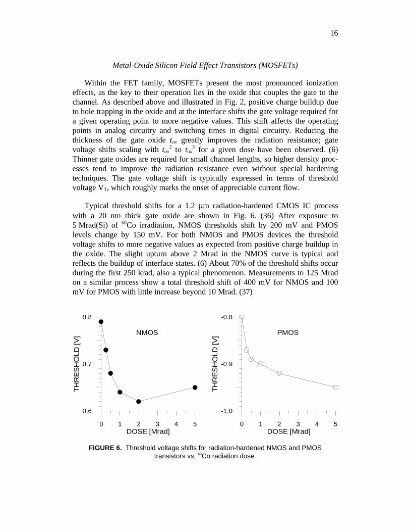
Typical threshold shifts for a 1.2 µm radiation-hardened CMOS IC processwith a 20 nm thick gate oxide are shown in Fig. 6. (36) After exposure to5 Mrad(Si) of 60Co irradiation, NMOS thresholds shift by 200 mV and PMOSlevels change by 150 mV. For both NMOS and PMOS devices the thresholdvoltage shifts to more negative values as expected from positive charge buildup inthe oxide. The slight upturn above 2 Mrad in the NMOS curve is typical andreflects the buildup of interface states. (6) About 70% of the threshold shifts occurduring the first 250 krad, also a typical phenomenon. Measurements to 125 Mradon a similar process show a total threshold shift of 400 mV for NMOS and 100mV for PMOS with little increase beyond 10 Mrad. (37)
0 1 2 3 4 5DOSE [Mrad]
0.6
0.7
0.8
TH
RE
SH
OLD
[V]
0 1 2 3 4 5DOSE [Mrad]
-1.0
-0.9
-0.8
TH
RE
SH
OLD
[V]NMOS PMOS
FIGURE 6. Threshold voltage shifts for radiation-hardened NMOS and PMOStransistors vs. 60Co radiation dose.
17
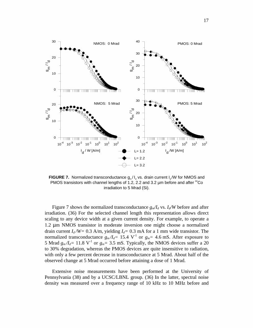
Figure 7 shows the normalized transconductance gm/Id vs. Id/W before and afterirradiation. (36) For the selected channel length this representation allows directscaling to any device width at a given current density. For example, to operate a1.2 µm NMOS transistor in moderate inversion one might choose a normalizeddrain current Id /W= 0.3 A/m, yielding Id= 0.3 mA for a 1 mm wide transistor. Thenormalized transconductance gm /Id= 15.4 V-1 or gm= 4.6 mS. After exposure to5 Mrad gm /Id= 11.8 V-1 or gm= 3.5 mS. Typically, the NMOS devices suffer a 20to 30% degradation, whereas the PMOS devices are quite insensitive to radiation,with only a few percent decrease in transconductance at 5 Mrad. About half of theobserved change at 5 Mrad occurred before attaining a dose of 1 Mrad.
Extensive noise measurements have been performed at the University ofPennsylvania (38) and by a UCSC/LBNL group. (36) In the latter, spectral noisedensity was measured over a frequency range of 10 kHz to 10 MHz before and
0
10
20
30
gm
/ I d
10-4
10-3
10-2
10-1
100
101
102
Id / W [A/m]
0
10
20
gm
/ Id
NMOS: 5 Mrad
NMOS: 0 Mrad
0
10
20
30
40
gm
/ I d
10-4
10-3
10-2
10-1
100
101
102
Id /W [A/m]
0
10
20
30
gm
/ Id
PMOS: 0 Mrad
PMOS: 5 Mrad
L= 1.2
L= 2.2
L= 3.2
FIGURE 7. Normalized transconductance gm / Id vs. drain current Id /W for NMOS andPMOS transistors with channel lengths of 1.2, 2.2 and 3.2 µm before and after 60Co
irradiation to 5 Mrad (Si).
18
after 60Co irradiation to a dose of 5 Mrad(Si). The noise was measured at threerepresentative drain current densities Id/W. Again, these data can be scaled to anydevice width, where the noise scales with W -1/2. The difference between theNMOS and PMOS results is striking. The NMOS devices show a much greaterdegradation and the PMOS devices also exhibit substantially less low-frequencynoise. The low-frequency noise spectral density of the NMOS devices can bedescribed by vn
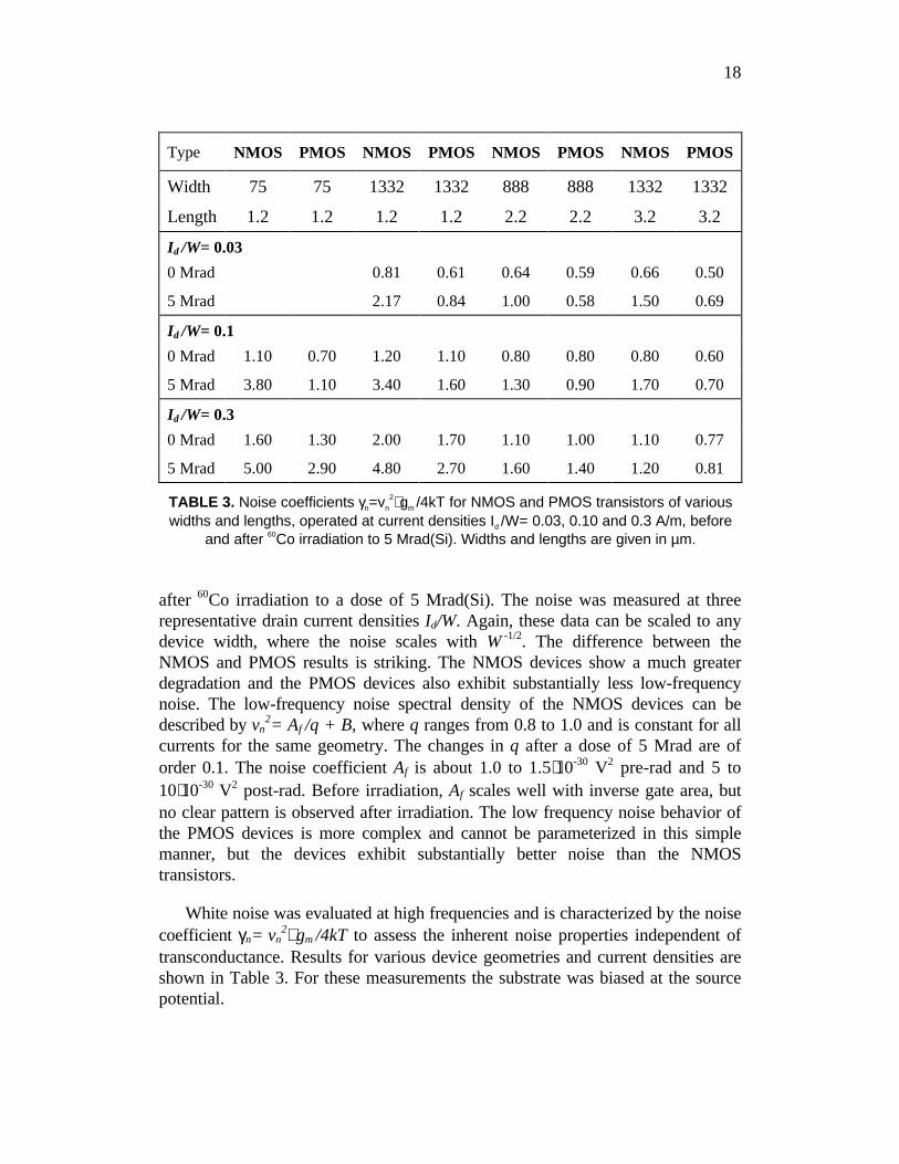
2= Af /q + B, where q ranges from 0.8 to 1.0 and is constant for allcurrents for the same geometry. The changes in q after a dose of 5 Mrad are oforder 0.1. The noise coefficient Af is about 1.0 to 1.5⋅10-30 V2 pre-rad and 5 to10⋅10-30 V2 post-rad. Before irradiation, Af scales well with inverse gate area, butno clear pattern is observed after irradiation. The low frequency noise behavior ofthe PMOS devices is more complex and cannot be parameterized in this simplemanner, but the devices exhibit substantially better noise than the NMOStransistors.
White noise was evaluated at high frequencies and is characterized by the noisecoefficient γn= vn
2⋅ gm /4kT to assess the inherent noise properties independent oftransconductance. Results for various device geometries and current densities areshown in Table 3. For these measurements the substrate was biased at the sourcepotential.
Type NMOS PMOS NMOS PMOS NMOS PMOS NMOS PMOS
Width 75 75 1332 1332 888 888 1332 1332
Length 1.2 1.2 1.2 1.2 2.2 2.2 3.2 3.2
Id /W= 0.03
0 Mrad 0.81 0.61 0.64 0.59 0.66 0.50
5 Mrad 2.17 0.84 1.00 0.58 1.50 0.69
Id /W= 0.1
0 Mrad 1.10 0.70 1.20 1.10 0.80 0.80 0.80 0.60
5 Mrad 3.80 1.10 3.40 1.60 1.30 0.90 1.70 0.70
Id /W= 0.3
0 Mrad 1.60 1.30 2.00 1.70 1.10 1.00 1.10 0.77
5 Mrad 5.00 2.90 4.80 2.70 1.60 1.40 1.20 0.81
TABLE 3. Noise coefficients γn=vn
2⋅ gm /4kT for NMOS and PMOS transistors of variouswidths and lengths, operated at current densities Id /W= 0.03, 0.10 and 0.3 A/m, before
and after 60Co irradiation to 5 Mrad(Si). Widths and lengths are given in µm.
19
Again, we see substantially less post-radiation degradation in the PMOSdevices. One can also observe the higher intrinsic noise of NMOS short channeldevices. Although the observed degradation is quite small in some cases, typicallyit is quite substantial and would need to be compensated for by a considerablyhigher operating current. Seller et al. have exposed low-noise preamplifiers fabri-cated in a rad-hard 1.2 µm bulk CMOS process to a dose of 100 Mrad and meas-ured noise and gain. (37) Gain decreased by no more than 7%, but the increase inequivalent input noise at high frequencies ranged from 20 to 75%. This process isonly specified to 5 Mrad, so these results indicate that circuits are still quite usableat much higher doses, if one can accommodate the increase in noise.
Due to the presence of mobile trapped charge, threshold behavior can becomequite difficult to predict when the gate voltage changes appreciably with varyingduty cycles, as in logic circuitry. Detectors and analog circuitry are simpler bycomparison, since the voltage levels are either static or change with a fixed period,as in analog pipelines, for example. In general, when performing ionization damagetests devices must be operated at typical operating voltages and digital circuitrymust be clocked at frequencies and patterns approximating typical operation.
Generally speaking, both bulk and SOI (silicon on insulator) CMOS are subjectto the effects described above. SOI is often cited as a specifically radiation-hardtechnology because of its resistance to transient radiation effects, primarily latchupdue to photocurrents developed at high intensity bursts of radiation(>106 -107 rad/s) typical of nuclear detonations. Although SOI can providesuperior device speed because of reduced stray capacitance, this technology is notinherently more resistant to radiation in our applications. If anything, the additionaloxide interfaces tend to complicate matters and at this time most radiation-resistantCMOS processes are on bulk silicon.
Radiation Effects in Integrated Circuit Structures
The preceding discussion has emphasized the properties of individual devices.In integrated circuits many devices are placed close together. As mentioned above,the silicon surface is naturally n-type, so isolation structures are required topreclude unwanted cross-coupling between devices. Two basic techniques areused:
• junction isolation, where reverse-biased pn junctions provide both ohmic andcapacitive isolation.
• oxide isolation, where oxide layers with carefully controlled interfaceproperties deplete the adjacent silicon of mobile charge.
20
More detailed information on these processes can be in texts on IC technology, forexample (39).
Junction isolation is very robust, but requires substantial additional space.Oxide isolation allows higher packing densities and is used by most high-density ICprocesses. All CMOS processes utilize some form of oxide isolation, whereasbipolar transistor processes can be found with both junction and oxide isolation.Under irradiation the oxide layers used for isolation suffer from the same phenom-ena described for the gate oxide of MOSFETs (see field oxide in Fig. 2). Sinceisolation oxides are thicker than gate oxides, more electron-hole pairs are formedby incident radiation. Furthermore, the fields in the isolation oxide tend to be muchlower, so charge trapping in the oxide will be exacerbated. Developing radiation-hard isolation oxides (field oxides) was a major challenge in the development ofhigh-density radiation-hard CMOS and remains one of the few “secret” processingredients (for a basic discussion see (6)).
Problems can occur when inherently radiation-hard devices, notably JFETs andbipolar transistors, are used in a non-hardened oxide-isolated processes. Hereradiation effects in the isolation structures can severely affect the radiation resis-tance of the devices. Clues to the importance of such parasitic ionization effectscan be gleaned from a comparison of neutron and photon irradiations. Conven-tional (non-hardened) processes using oxide isolation have yielded good results inmeasurements to fluences >1014 cm-2 (27,28), demonstrating that oxide isolationcan be acceptable and that the suitability of these processes must be determinedcase-by-case.
IC processes also use special device structures to facilitate the integration ofdifferent device types. A prime example is the lateral pnp transistor, a structuremore compatible with a standard CMOS process than “classic” vertical bipolartransistors. In a lateral transistor the emitter, base and collector are arranged alongthe surface of the silicon with large-area exposure to oxide interfaces. Unlikevertical bipolar transistors, lateral devices are very susceptible to ionizing radiation,as surface leakage causes severe degradation of DC current gain. Lateral pnptransistors can be used as current sources or high impedance loads, if the biasingcircuitry is designed to accommodate substantial increases in base currents.
MITIGATION TECHNIQUES
Although little can be done to reduce radiation damage in a given device,many techniques can be applied to reduce the effects of radiation damage to anoverall system. The goal of radiation-hard design is not so much to obtain a systemwhose characteristics do not change under irradiation, rather than to maintain the

21
required performance characteristics over the lifetime of the system. The formerapproach tends to utilize mediocre to poor technologies that remain so over thecourse of operation. The latter starts out with superior characteristics, whichgradually deteriorate under irradiation. Depending on the specific system, thesedesigns may die gradually, although at some fluence or dose a specific circuit, typi-cally digital, may cease to function at all. Clearly, the best mitigation technique isto avoid the problem, either by shielding or by reducing the electronics in theradiation environment to the minimum required to do the job. The latter runscounter to prevailing trends, which favor digitizing as close to the front-end aspossible and tend to implement even simple control functions with digital circuitry.
Detectors
Increased detector leakage current has several undesirable consequences.
1. The integrated current over typical signal processing times can greatlyexceed the signal.
2. Shot noise increases.
3. The power dissipated in the detectors increases (Idet⋅Vdet)
Since the leakage current decreases exponentially with temperature, cooling isthe simplest technique to reduce diode leakage current. For example, reducing thedetector temperature from room temperature to 0 °C reduces the bias current toabout 1/6 of its original value.
Detector power dissipation is a concern in large-area silicon detectors for theLHC, where the power dissipation in the detector diode itself can be of order 1 to10 mW/cm2. Since the leakage current is an exponential function of temperature,local heating will increase the leakage current, which will increase the localheating, and so on, ultimately taking the device into thermal runaway. To avoidthis potentially catastrophic failure mode, the cooling system must be designed toprovide sufficient cooling of the detector, a challenging (but apparently doable)task in a system that is to have zero mass.
Reducing the integration time reduces both baseline changes due to integrateddetector current and shot noise. Clearly, this is limited by the duration of the signalto be measured. To some degree, circuitry can be designed to accommodate largebaseline shifts due to detector current, but at the expense of power. AC coupleddetectors eliminate this problem. In instrumentation systems that require DCcoupling, correlated double sampling techniques can be used to sample the baselinebefore the signal occurs and then subtract from the signal measurement.
22
One of the most powerful measures against detector leakage current issegmentation. For a given damage level, the detector leakage current per signalchannel can be reduced by segmentation. If a diode with a leakage current of10 µA is subdivided into 100 subelectrodes each with its own signal processingchannel, the DC current in each channel will be 100 nA and shot noise reduced bya factor of 10. This is why large area silicon tracking detectors can survive in theLHC environment. Fortuitously, increased segmentation is also required to dealwith the high event rate. Pixel detectors with small electrode areas offer greatadvantages in this regard.
The most severe restriction on radiation resistance is imposed by type inver-sion, where the net acceptor concentration at some fluence becomes so large thatthe detector will no longer sustain the required voltage for full depletion. This isespecially critical for position-sensing detectors with electrodes on both sides(double-sided detectors), for which full depletion is essential.
One can circumvent the type-inversion limit by using back-to-back single-sideddetectors. The initial configuration uses n type segmented strip electrodes on nbulk, with a contiguous p electrode on the backside. Initially, the pn-junction is atthe backside. This does require full depletion in initial operation, but this is noproblem for the non-irradiated device and becomes easier to maintain as increasingfluence moves the bulk towards type inversion. After type inversion the bulkbecomes p type and the junction shifts to the n electrodes, so that the bulk aroundthe electrodes will be depleted and maintain inter-electrode isolation even in partialdepletion.
Electronics
The design of the electronic systems is governed by changes in transistorparameters under irradiation, but circuit design and, at a higher level, architectureare equally important. Amplifiers are sensitive to changes in gain, bandwidth, andnoise, so that effects on transconductance and noise parameters are important.Comparators used for threshold determination and timing rely critically onthreshold shifts. Analog storage cells and switched capacitor systems tend to besensitive to leakage currents. Digital circuitry is affected by threshold shifts thataffect propagation delays and device transconductance, which determinesswitching speed.
Shorter shaping times improve tolerance to leakage currents. In high ratesystems, fast response time is needed anyway, so experimental desires andengineering considerations interfere constructively. Since the system must bedesigned to tolerate a substantial shot noise current, utilization of bipolar junctiontransistors becomes very attractive, since the base shot noise becomes a minor
23
contribution (in contrast to systems that emphasize noise minimization, as in x-rayspectrometry or liquid argon calorimetry).
In general, for use in amplifiers bipolar transistor circuitry is superior toCMOS. In logic circuitry, especially at low overall switching rates, CMOS isadvantageous both because of power consumption and circuit density. For exam-ple, the on-detector silicon tracker front-end under development for the ATLASexperiment at the LHC uses bipolar transistor technology for the amplifier-pulseshaper-comparator and radiation-hard CMOS for a clock-driven digital pipelinebuffer and data readout.
In amplifiers, bipolar transistors offer higher bandwidth for a given power andsuperior device matching, which is a prime consideration in highly segmentedsystems with a correspondingly large number of channels. Threshold shifts inbipolar transistors are quite small with excellent matching between devices. JFETsyield excellent noise performance in applications where power consumption andcircuit density are not prime considerations. Even when a CMOS front-end ischosen, because of the use of a switched capacitor analog memory, or the desire tocombine the analog and digital circuitry on the same chip, amplifiers can be madequite radiation resistant, since the circuitry can be made to adjust for shifts inthreshold voltage.
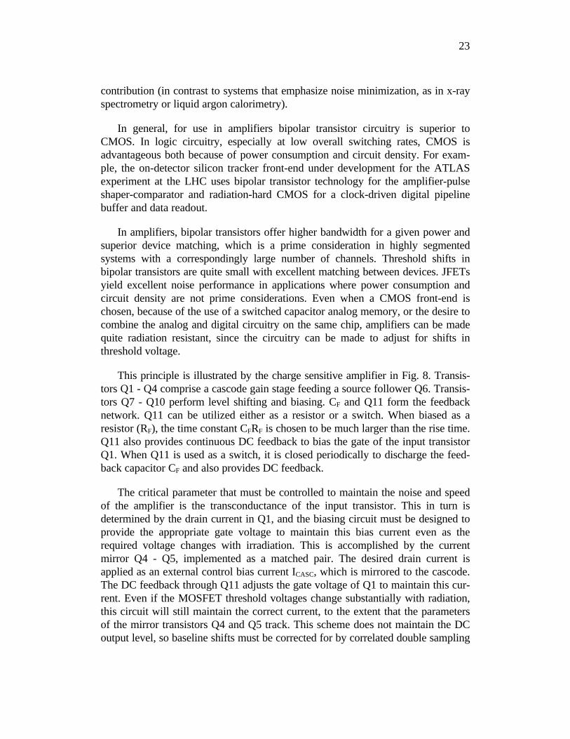
This principle is illustrated by the charge sensitive amplifier in Fig. 8. Transis-tors Q1 - Q4 comprise a cascode gain stage feeding a source follower Q6. Transis-tors Q7 - Q10 perform level shifting and biasing. CF and Q11 form the feedbacknetwork. Q11 can be utilized either as a resistor or a switch. When biased as aresistor (RF), the time constant CFRF is chosen to be much larger than the rise time.Q11 also provides continuous DC feedback to bias the gate of the input transistorQ1. When Q11 is used as a switch, it is closed periodically to discharge the feed-back capacitor CF and also provides DC feedback.
The critical parameter that must be controlled to maintain the noise and speedof the amplifier is the transconductance of the input transistor. This in turn isdetermined by the drain current in Q1, and the biasing circuit must be designed toprovide the appropriate gate voltage to maintain this bias current even as therequired voltage changes with irradiation. This is accomplished by the currentmirror Q4 - Q5, implemented as a matched pair. The desired drain current isapplied as an external control bias current ICASC, which is mirrored to the cascode.The DC feedback through Q11 adjusts the gate voltage of Q1 to maintain this cur-rent. Even if the MOSFET threshold voltages change substantially with radiation,this circuit will still maintain the correct current, to the extent that the parametersof the mirror transistors Q4 and Q5 track. This scheme does not maintain the DCoutput level, so baseline shifts must be corrected for by correlated double sampling
24
or rendered irrelevant by AC coupling. The operating voltage and the gate volt-ages of the cascode transistors Q2 and Q3 must be chosen somewhat higher thanfor unirradiated operation to accommodate the threshold shifts, so overall powerdissipation will be somewhat higher. Techniques of this type can provide radiation-resistant amplifiers with radiation-soft transistors.
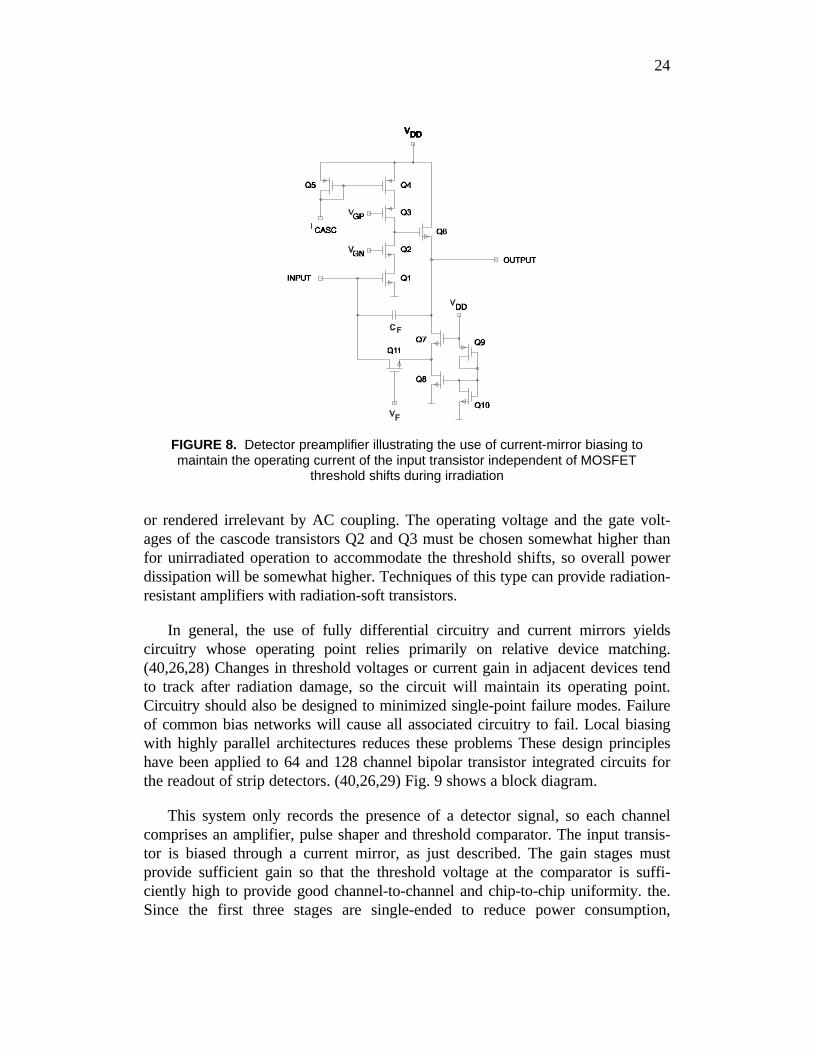
In general, the use of fully differential circuitry and current mirrors yieldscircuitry whose operating point relies primarily on relative device matching.(40,26,28) Changes in threshold voltages or current gain in adjacent devices tendto track after radiation damage, so the circuit will maintain its operating point.Circuitry should also be designed to minimized single-point failure modes. Failureof common bias networks will cause all associated circuitry to fail. Local biasingwith highly parallel architectures reduces these problems These design principleshave been applied to 64 and 128 channel bipolar transistor integrated circuits forthe readout of strip detectors. (40,26,29) Fig. 9 shows a block diagram.
This system only records the presence of a detector signal, so each channelcomprises an amplifier, pulse shaper and threshold comparator. The input transis-tor is biased through a current mirror, as just described. The gain stages mustprovide sufficient gain so that the threshold voltage at the comparator is suffi-ciently high to provide good channel-to-channel and chip-to-chip uniformity. the.Since the first three stages are single-ended to reduce power consumption,
FIGURE 8. Detector preamplifier illustrating the use of current-mirror biasing tomaintain the operating current of the input transistor independent of MOSFET
threshold shifts during irradiation
25
substantial circuit complexity would be necessary to maintain DC stability, so ACcoupling is introduced at the input of the third stage. From here on the circuitry isdifferential. The third stage is still single-ended, but it is replicated as a dummyamplifier to bias the second input of the differential amplifier. The dummy amplifieris included in each individual channel to obtain optimal parameter tracking underradiation damage, and also to maintain a parallel architecture and reduce single-point failure modes. The threshold level is applied differentially to exploit devicetracking during irradiation.
The design of CMOS logic circuitry does not offer the flexibility of self-adjusting circuitry. Since the threshold shifts of n and p MOSFETs are not com-plementary, circuit switching thresholds change. At high damage levels the devicetransconductance also suffers due to buildup of interface charge and increasedscattering of charge carriers in the channel. Both effects change propagationdelays, which can lead to race conditions (mismatches in propagation delays ofstreams whose results are combined) that cause circuit failure. These problems canbe mitigated somewhat by careful design, but they point out a qualitative criterionfor radiation resistant system design: complexity. As a general rule, simple logiccircuitry can be made more radiation resistant than complex circuitry that requiresrelative control of many mixed serial and parallel paths. Fully clocked systemsavoid this problem, but at substantial penalties in power, speed, and area. Carefulconsideration should be given before incorporating complete wish-lists of circuitry(on-chip digitization, digital signal processing, microprocessor controlled readout,etc.) in a severe radiation environment (apart from common-sensical considera-tions such as reliability and maintenance of components that are not accessiblewithout major disassembly). Simplest tends to be best.
THRESHOLD ADJUST
TEST INPUT
GAIN/SHAPER COMPARATOR
DET.
PREAMP
OUTPUT
FIGURE 9. Block diagram of a readout channel for strip detectors.
26
IMPLEMENTATIONS
Several ICs for high-energy physics using the radiation-hard CMOS areinstalled in running experiments. Clock-driven pipelines designed for ZEUS andSDC have been fabricated and tested, and are operating successfully. The SVX ICdesigned for the CDF silicon vertex detector has been transferred to the rad-hardUTMC process. SVX-H ICs are installed in both CDF and L3 (41) and areproviding excellent results. All of these are full-custom designs, which allowcontrol over device and process selection. Otherwise, the use of a non-hardenedbipolar transistor IC process (26,28) would be extremely risky. However, fullcustom technology may not be required in all applications.
In many instrumentation applications discrete designs are suitable. As shownabove, bipolar transistors and JFETs can provide very high radiation resistancewithout resorting to qualified radiation-hard devices. The same typically holds forECL logic ICs. If the ionizing dose does not exceed several 100 krad, standardsub-micron CMOS may be adequate, because the thinner gate oxides (~ 20 nm)required in short channel devices provide a significant improvement in thresholdshift with respect to the 50 nm oxides of earlier 3 µm devices. One caveat is inorder, however. The radiation characteristics of standard (non rad-hard) CMOSprocesses are inherently unpredictable from lot to lot. If devices from a givenproduction run are tested and found satisfactory (including a substantial perform-ance margin), devices from the same lot should be used in the final system. Thispractice should be followed with any “off the shelf” IC that is not radiation-qualified. Especially if the system is readily accessible for maintenance orreplacement, this course may be quite acceptable.
A more reliable approach is to use radiation-qualified transistors and ICs avail-able commercially as standard parts. Power MOSFETs are offered with full speci-fications to 1 Mrad and limited use to 3 Mrad. Displacement damage is specified to1014 n/cm2. Operational amplifiers are available with guaranteed specifications to 1Mrad(Si). CMOS logic ICs (inverters, gates, flip-flops, shift registers) are alsospecified to 1 Mrad. As mentioned above, the circuit design must accommodateincreased propagation delay and reduced clock rates. Devices with higher integra-tion levels are also available, for example 32K x 8 SRAMs specified to 300 krad.20 MSPS 8 bit flash ADCs implemented in 1.25 µm junction isolated rad-hardCMOS have been tested to 81 Mrad 60Co with no loss in performance (42).
The last example is also a reminder of a phenomenon that has been illustratedabove (37) and observed repeatedly. (43) The typical pattern is that parameterschange most up to 1 Mrad and then plateau. Modern radiation-hard CMOSdevices perform well at doses well beyond their rated maximum dose. The reasonfor this is the expense of fully qualifying a radiation-hard process in accordance
27
with the requirements of the military and aerospace agencies, so devices areguaranteed only to the required specification, rather than the capabilities of thefabrication process.
CONCLUSION
Judicious evaluation of the radiation fields coupled with a stringent analysis ofapplication requirements can yield electronic systems capable of performing well toionizing doses of 100 Mrad and particle fluences of 1014 and probably 1015 cm-2.Developing radiation-resistant systems does require great attention to detail andsubstantially more testing effort than conventional designs, but the effort isnecessary if we are to exploit the high-luminosity accelerators on the horizon. Formany applications we are limited less by technology than by ingenuity.
This work was supported by the US Department of Energy, Office of High Energyand Nuclear Physics.
BIBLIOGRAPHY
Semiconductor device and integrated circuit technology
1. Grove, A.S., Physics and Technology of Semiconductor Devices (John Wiley& Sons, New York, 1967)
2. Sze, S.M., Physics of Semiconductor Devices (John Wiley & Sons, New York,1981) TK 7871.85.S988, ISBN 0-471-05661-8
3. Nicollian, E.H. and Brews, J.R., MOS (Metal Oxide Semiconductor) Physicsand Technology (John Wiley & Sons, New York, 1982) TK7871.99.M44N52,ISBN 0-471-08500-6
4. Wolf, S., Silicon Processing for the VLSI Era, Volume 2 - Process Integration(Lattice Press, Sunset Beach, 1990) ISBN 0-961672-4-5
28
Radiation Effects
1. Ma, T.P. and Dressendorfer, P.V., Ionizing Radiation Effects in MOS Devicesand Circuits (John Wiley & Sons, New York, 1989) TK7871.99.M44I56,ISBN 0-471-84893-X
2. Messenger, G.C. and Ash, M.S., The Effects of Radiation on ElectronicSystems (van Nostrand Reinhold, New York, 1986) TK7870.M4425, ISBN 0-442-25417-2
3. Srour, J.R. et al., Radiation Effects on and Dose Enhancement of ElectronicMaterials (Noyes Publications, Park Ridge, 1984) TK7870.R318, ISBN 0-8155-1007-1
4. van Lint, V.A.J. et al., Mechanisms of Radiation Effects in ElectronicMaterials (John Wiley & Sons, New York, 1980) TK7871.M44, ISBN 0-471-04106-8
Journals
Most papers on radiation effects in semiconductor devices are presented at theIEEE Nuclear and Space Radiation Effects Conference and published in the annualconference issue (usually December) of the IEEE Transactions on NuclearScience. Additional papers, primarily from the high energy physics community, arepublished in the Conference Record of the IEEE Nuclear Science Symposium andin the conference issue of the IEEE Transactions on Nuclear Science. Otherconferences on detector instrumentation tend to publish their proceedings inNuclear Instruments and Methods. Many of the new results on detectors (Si andGaAs) and low-noise front-ends appear as internal notes of the ATLAS and CMScollaborations in preparation for the LHC.
REFERENCES
1. http://www-atlas.lbl.gov/strips/doc/tutorials.html
2. Messenger, G.C. and Ash, M.S., The Effects of Radiation on ElectronicSystems (van Nostrand Reinhold, New York, 1986), p. 166
3. Burke E.A., “Energy Dependence of Proton-Induced Displacement Damagein Silicon,” IEEE Trans. Nucl. Sci. NS-33/6, 1276 (1986)
4. Van Ginneken A., “Non Ionizing Energy Deposition in Silicon for RadiationDamage Studies,” FNAL FN 522 (October, 1989)
29
5. Srour, J.R. et al., “Radiation Damage Coefficients for Silicon DepletionRegions,” IEEE Trans. Nucl. Sci. NS26/6, 4784 (1979)
6. Ma, T.P. and Dressendorfer, P.V., Ionizing Radiation Effects in MOSDevices and Circuits (John Wiley & Sons, New York, 1989)
7. Tsveybak, I. et al., “Fast Neutron-Induced Changes in Net ImpurityConcentration of High-Resistivity Silicon,” IEEE Trans. Nucl. Sci. NS-39/6, 1720-1729 (1992)
8. Barberis, E. et al., “Temperature effects on radiation damage to silicondetectors,” Nucl. Instr. and Meth. A326, 373-380 (1993)
9. Chilingarov, A. et al., “Radiation Hardness of the Silicon Counter Tracker(SCT) for ATLAS,” Proceedings of the 27th International Conference onHigh Energy Physics, Glasgow, July 20-27, 1994, contribution 0943
10. Sze, S.M., Physics of Semiconductor Devices (John Wiley & Sons, NewYork, 1981), p. 90
11. Gill, K. et al., “Radiation damage by neutrons and photons to silicondetectors,” Nucl. Instr. and Meth. A322, 177 (1992)
12. Ohsugi, T. et al., “Radiation Damage in Silicon Microstrip Detectors,”Nucl. Instr. and Meth. A265, 105-111 (1988)
13. Li, Z., “Modeling and simulation of neutron induced changes andtemperature annealing of Neff and changes in resistivity in high resistivitysilicon detectors,” Nucl. Instr. and Meth. A342, 105-118 (1994)
14. Pitzl, D. et al., “Type Inversion in Silicon Detectors,” Nucl. Instr. and Meth.A311, 98 (1992)
15. Giubellino, P. et al., “Study of the Effects of Neutron Irradiation on SiliconStrip Detectors,” Nucl. Instr. and Meth. A315, 156 (1992)
16. Matthews, J.A.J. et al., “Bulk Radiation Damage in Silicon Detectors andImplications for ATLAS SCT,” New Mexico Center for Particle PhysicsNote and ATLAS INDET-NO-118, 1995
17. Ziock, H.-J. et al., “Temperature dependence of the radiation inducedchange of depletion voltage in silicon PIN detectors,” Nucl. Instr. andMeth. A342, 96-104 (1994)

30
18. Lemeilleur, F. et al., “Neutron-induced radiation damage in silicondetectors,” IEEE Trans. Nucl. Sci. NS-39/4, 551-557 (1992)
19. Fretwurst, E. et al., “Radiation Hardness of Silicon Detectors for FutureColliders,” Nucl. Instr. and Meth. A326, 357-364 (1993)
20. Tamura, N. et al., “Radiation effects of double-sided silicon strip detectors,”Nucl. Instr. and Meth. A342, 131-136 (1994)
21. Unno, Y. et al., to be published in IEEE Trans. Nucl. Sci.
22. Barberis, E. et al., “Capacitances in silicon microstrip detectors,” Nucl.Instr. and Meth. A342, 90-95 (1994)
23. Wheadon, R. et al., “Radiation tolerance studies of silicon microstripdetectors for the LHC,” Nucl. Instr. and Meth. A342, 126-130 (1994)
24. Kubota, M. et al., “Radiation Damage of Double-Sided Silicon StripDetectors,” Conference Record of the 1991 IEEE Nuclear ScienceSymposium and Medical Imaging Conference, Nov. 2 - 9, 1991, Santa Fe,New Mexico, Vol. 1, p. 246
25. Messenger, G.C. and Ash, M.S., The Effects of Radiation on ElectronicSystems (van Nostrand Reinhold, New York, 1986), p. 183
26. I. Kipnis et al., “An Analog Front-End Bipolar-Transistor IC for the SDCSilicon Tracker,” IEEE Trans. Nucl. Sci. NS-41/4, 1095-1103 (1994)
27. Cartiglia, N. et al., “Radiation Hardness Measurements on Bipolar TestStructures and an Amplifier-Comparator Circuit,” Conference Record ofthe IEEE Nuclear Science Symposium, Oct. 25-31, 1992, Orlando, Florida(ISBN 0-7803-0883-2), Vol. 2, pp. 819-821, 1992
28. Spencer, E. et al., “A Fast Shaping Low Power Amplifier-ComparatorIntegrated Circuit for Silicon Strip Detectors,” IEEE Trans. Nucl. Sci.NS-42/4, 796-802 (1995)
29. Kipnis, I., “CAFE: A Complementary Bipolar Front-End Integrated Circuitfor the ATLAS SCT,” on WWW at http://www-atlas.lbl.gov/strips/doc/reports.html
30. Kipnis, I., private communication
31. Sze, S.M., Physics of Semiconductor Devices (John Wiley & Sons, NewYork, 1981), pp. 314-322

31
32. Citterio, M. et al., “A Study of Low Noise JFETs Exposed to Large Dosesof Gamma Rays and Neutrons,” Conference Record of the IEEE NuclearScience Symposium, Oct. 25-31, 1992, Orlando, Florida (ISBN 0-7803-0883-2), Vol. 2, pp. 794-796, 1992
33. Citterio, M. et al., “Radiation Effects at Cryogenic Temperatures in Si-JFET, GaAs MESFET, and MOSFET Devices,” IEEE Trans. Nucl. Sci.NS-42/6, 2266-2270 (1995)
34. Radeka, V. et al., “JFET Monolithic Preamplifier with Outstanding NoiseBehavior and Radiation Hardness Characteristics,” IEEE Trans. Nucl. Sci.NS-40/4, 744-749 (1993)
35. Stephen, J.H., “Low noise field effect transistors exposed to intense ionizingradiation,” IEEE Trans. Nucl. Sci. NS-33/6, 1465-1470 (1986)
36. Dabrowski, W. et al., “Noise Measurements on Radiation-Hardened CMOSTransistors,” Conference Record of the 1991 IEEE Nuclear ScienceSymposium and Medical Imaging Conference, Nov. 2 - 9, 1991, Santa Fe,New Mexico, IEEE catalog no. 91CH3100-5, Vol. 3, pp. 1536-1540, 1991
37. Seller, P. et al., RAL-TR-95-055 and “ATLAS SCT Technical ProposalBackup Document,” ATLAS INDET-NO-085, 1995 (CERN)
38. Tedja, S. et al., “Noise Spectral Density Measurements of a Radiation-Hardened CMOS Process in the Weak and Moderate Inversion,” IEEETrans. Nucl. Sci. NS-39/4, 804-808 (1992)
39. Wolf, S., Silicon Processing for the VLSI Era, Volume 2 - ProcessIntegration (Lattice Press, Sunset Beach, 1990) ISBN 0-961672-4-5
40. Spieler, H., “Analog Front-End Electronics for the SDC Silicon Tracker,”Nucl. Instr. and Meth. A342, 205-213 (1994)
41. Acciarri, M. et al., “The L3 silicon microvertex detector,” CERN-PPE/94-122, 1994
42. Nutter, S. et al., “Results of Radiation Hardness Tests and PerformanceTests of the HS9008RH Flash ADC,” IEEE Trans. Nucl. Sci. NS-41/4(1994) 1197-1202
43. “ATLAS SCT Technical Proposal Backup Document,” ATLAS INDET-NO-085, 1995 (CERN)