Embed Size (px)
Citation preview
Digital Integrated Circuits © Prentice Hall 1995Memory
SEMICONDUCTOR MEMORIES
Digital Integrated Circuits © Prentice Hall 1995Memory
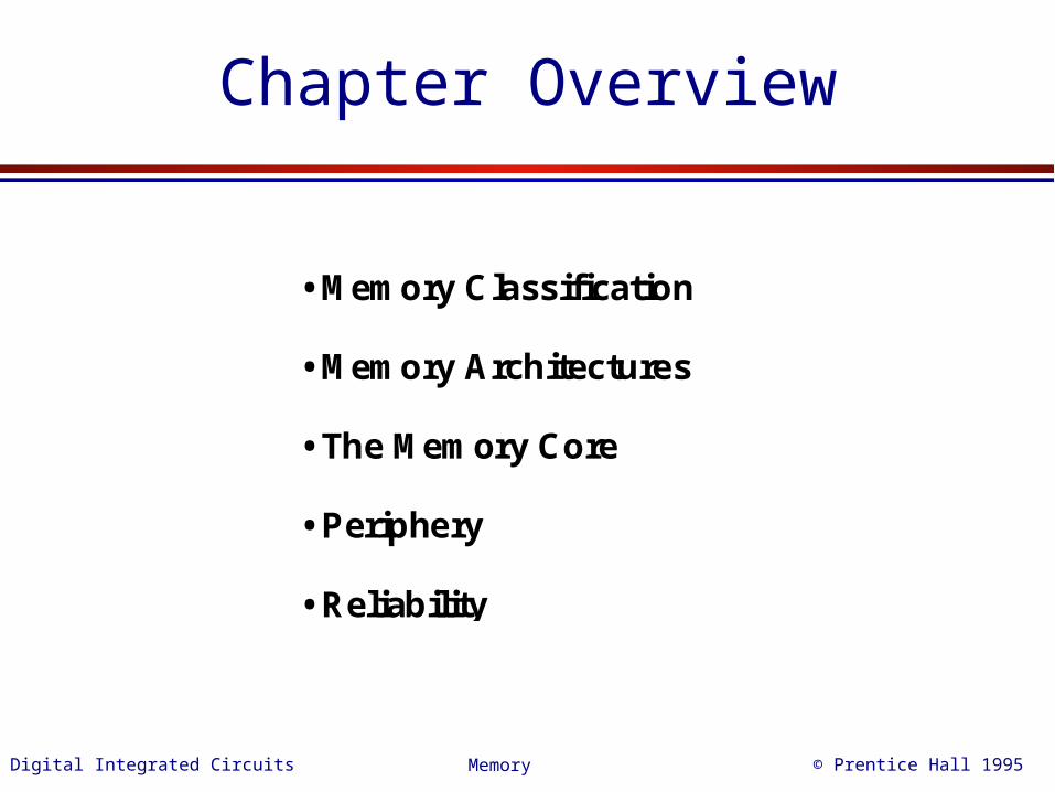
Chapter Overview
• Memory Classification
• Memory Architectures
• The Memory Core
• Periphery
• Reliability
Digital Integrated Circuits © Prentice Hall 1995Memory
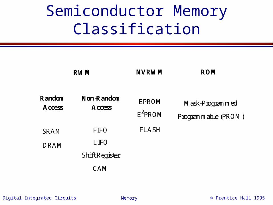
Semiconductor Memory Classification
RWM NVRWM ROM
EPROM
E2PROM
FLASH
RandomAccess
Non-RandomAccess
SRAM
DRAM
Mask-Programmed
Programmable (PROM)
FIFO
Shift Register
CAM
LIFO
Digital Integrated Circuits © Prentice Hall 1995Memory
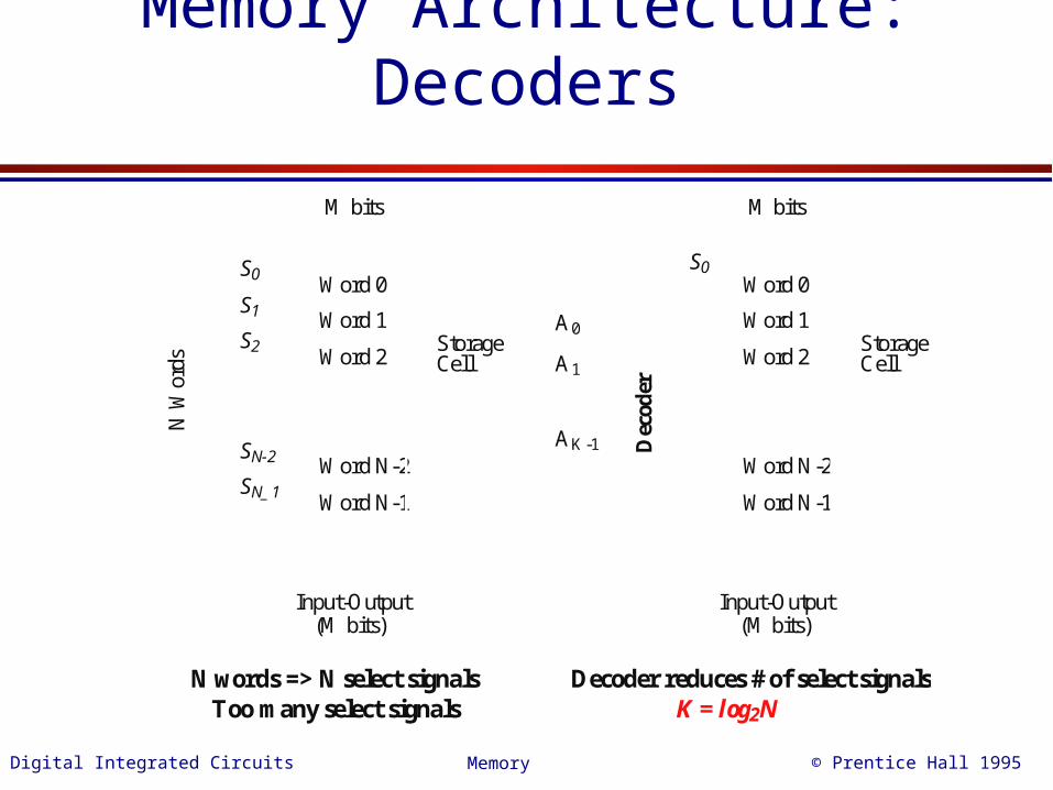
Memory Architecture: Decoders
Word 0
Word 1
Word 2
Word N-1
Word N-2
Input-Output
S0
S1
S2
SN-2
SN_1
(M bits)
StorageCell
M bits
N W
ords
Word 0
Word 1
Word 2
Word N-1
Word N-2
Input-Output(M bits)
StorageCell
M bits
Dec
oder
A0
A1
AK-1
S0
N words => N select signalsToo many select signals
Decoder reduces # of select signalsK = log2N
Digital Integrated Circuits © Prentice Hall 1995Memory
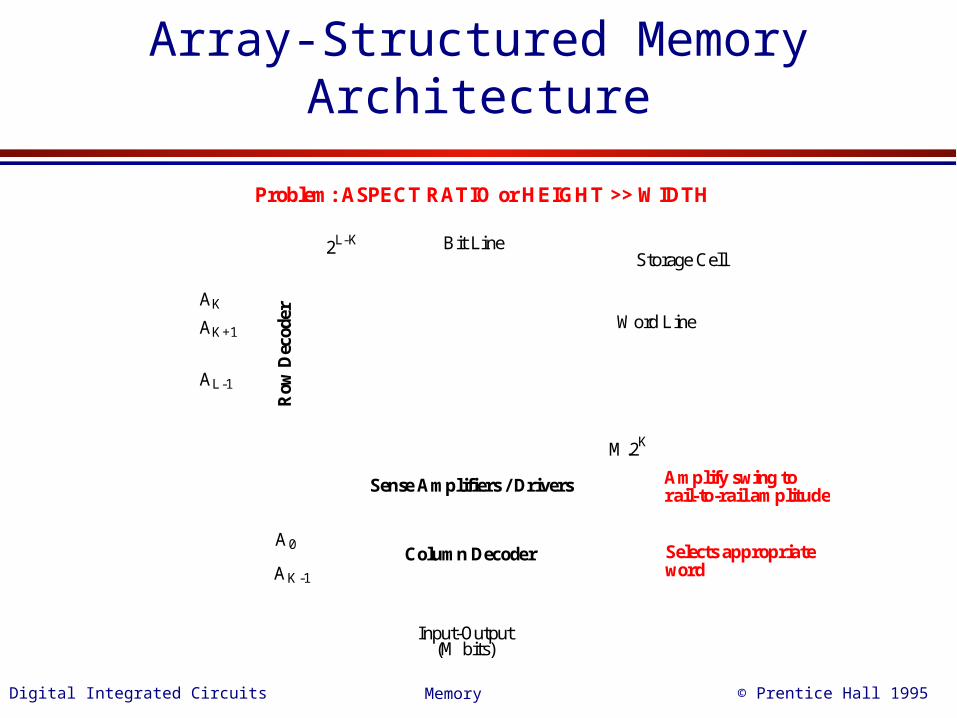
Array-Structured Memory Architecture
Input-Output(M bits)
Row
Dec
oder
AK
AK+1
AL-1
2L-K
Column Decoder
Bit Line
Word Line
A0
AK-1
Storage Cell
Sense Amplifiers / Drivers
M.2K
Problem: ASPECT RATIO or HEIGHT >> WIDTH
Amplify swing torail-to-rail amplitude
Selects appropriateword
Digital Integrated Circuits © Prentice Hall 1995Memory
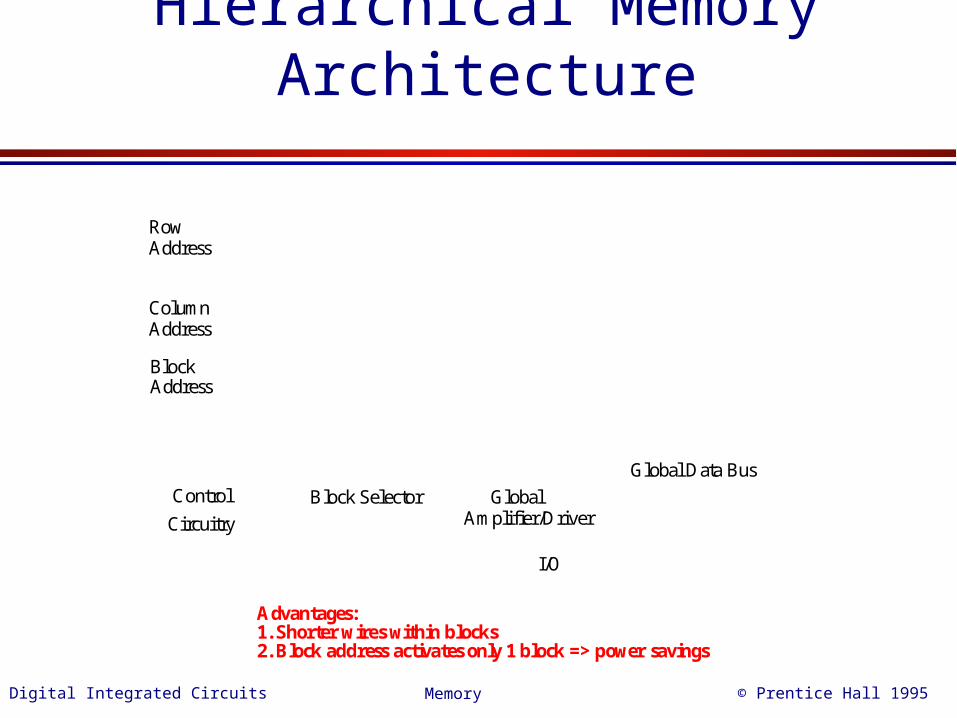
Hierarchical Memory Architecture
Global Data Bus
RowAddress
ColumnAddress
BlockAddress
Block Selector GlobalAmplifier/Driver
I/O
Control
Circuitry
Advantages:1. Shorter wires within blocks2. Block address activates only 1 block => power savings
Digital Integrated Circuits © Prentice Hall 1995Memory
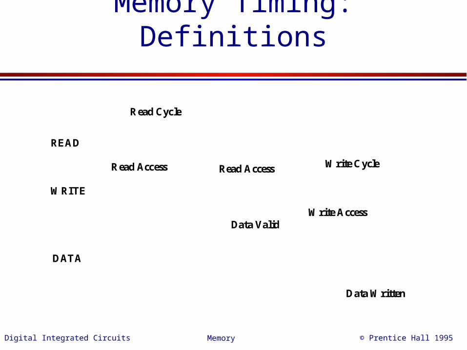
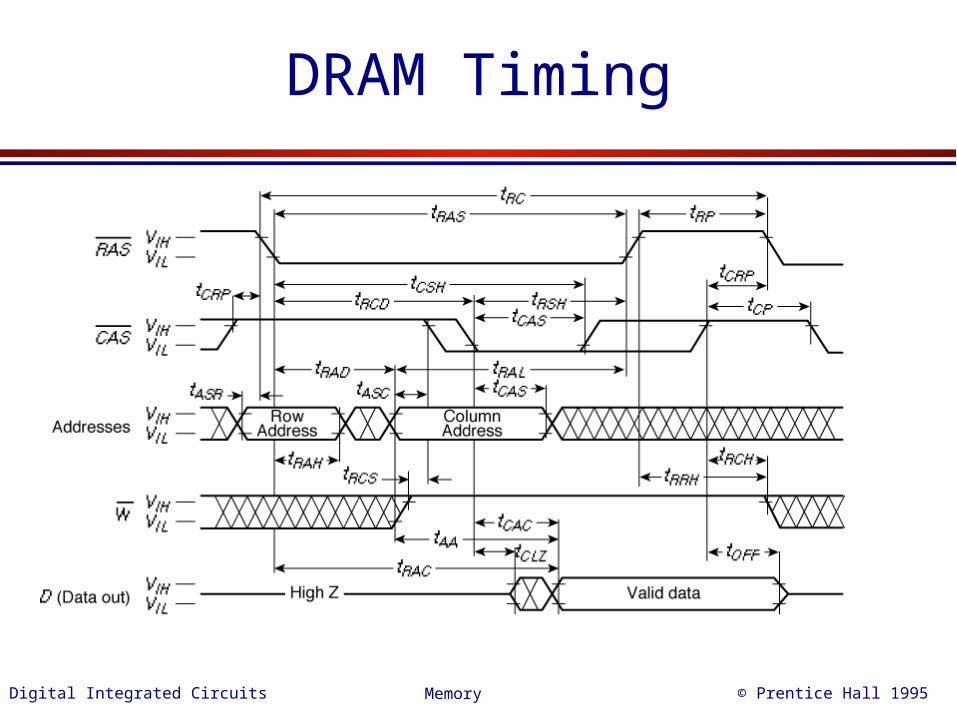
Memory Timing: Definitions
READ
WRITE
DATA
Read Access Read Access
Read Cycle
Data Valid
Data Written
Write Access
Write Cycle
Digital Integrated Circuits © Prentice Hall 1995Memory
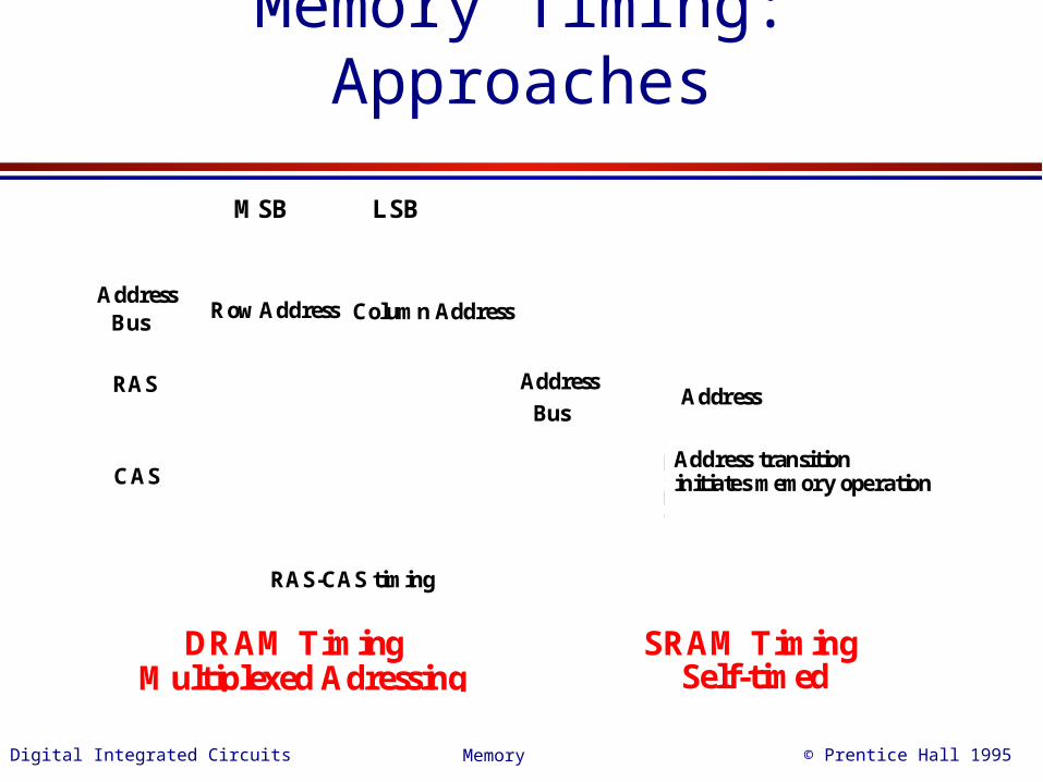
Memory Timing: Approaches
AddressBus
RAS
CAS
RAS-CAS timing
Address
BusAddress
Address transitioninitiates memory operation
DRAM Timing SRAM Timing
Row Address Column Address
MSB LSB
Multiplexed Adressing Self-timed
Digital Integrated Circuits © Prentice Hall 1995Memory
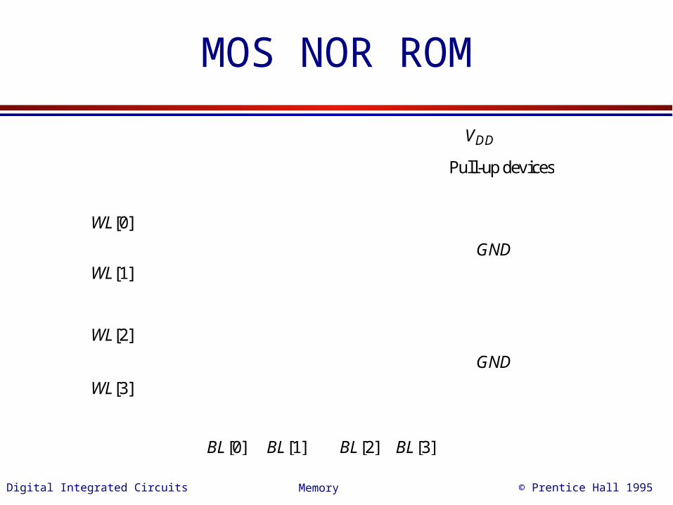
MOS NOR ROM
WL[0]
WL[1]
WL[2]
WL[3]
BL[0] BL[1] BL[2] BL[3]
GND
GND
VDD
Pull-up devices
Digital Integrated Circuits © Prentice Hall 1995Memory
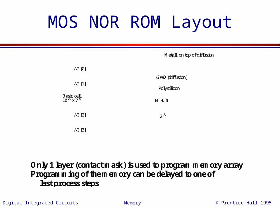
MOS NOR ROM Layout
Metal1 on top of diffusion
Basic cell10 x 7
2
WL[0]
WL[1]
WL[2]
WL[3]
GND (diffusion)
Metal1
Polysilicon
Only 1 layer (contact mask) is used to program memory arrayProgramming of the memory can be delayed to one of
last process steps
Digital Integrated Circuits © Prentice Hall 1995Memory
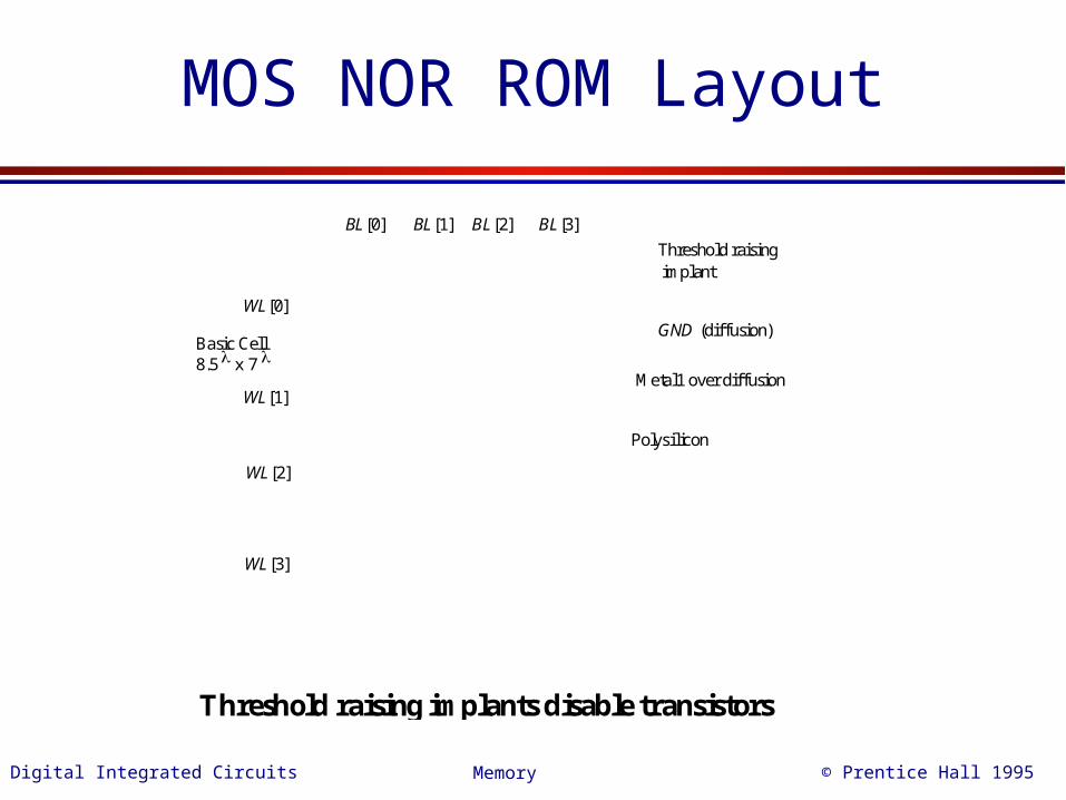
MOS NOR ROM Layout
Basic Cell8.5 x 7
WL[0]
WL[1]
WL[2]
WL[3]
Metal1 over diffusion
Threshold raisingimplant
BL[0] BL[1] BL[2] BL[3]
Polysilicon
GND (diffusion)
Threshold raising implants disable transistors
Digital Integrated Circuits © Prentice Hall 1995Memory
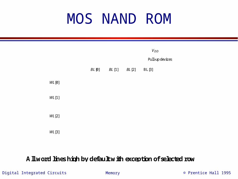
MOS NAND ROM
WL[0]
WL[1]
WL[2]
WL[3]
BL[0] BL[1] BL[2] BL[3]
VDD
Pull-up devices
All word lines high by default with exception of selected row
Digital Integrated Circuits © Prentice Hall 1995Memory
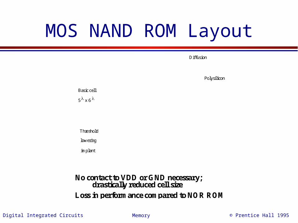
MOS NAND ROM Layout
Basic cell
5 x 6
Threshold
implant
Polysilicon
Diffusion
lowering
No contact to VDD or GND necessary;
Loss in performance compared to NOR ROMdrastically reduced cell size
Digital Integrated Circuits © Prentice Hall 1995Memory
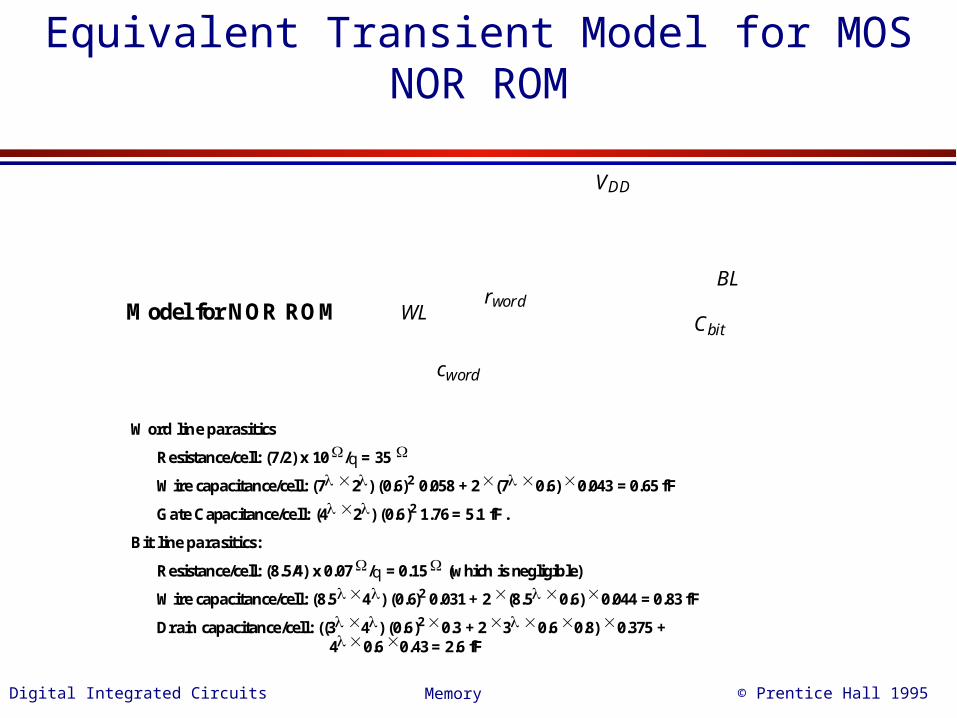
Equivalent Transient Model for MOS NOR ROM
VDD
WL
BLrword
cword
CbitModel for NOR ROM
Word line parasitics
Resistance/cell: (7/2) x 10 /q = 35
Wire capacitance/cell: (7 2) (0.6)2 0.058 + 2 (7 0.6) 0.043 = 0.65 fF
Gate Capacitance/cell: (4 2) (0.6)2 1.76 = 5.1 fF.
Bit line parasitics:
Resistance/cell: (8.5/4) x 0.07 /q = 0.15 (which is negligible)
Wire capacitance/cell: (8.5 4) (0.6)2 0.031 + 2 (8.5 0.6) 0.044 = 0.83 fF
Drain capacitance/cell: ((3 4) (0.6)2 0.3 + 2 3 0.6 0.8) 0.375 + 4 0.6 0.43 = 2.6 fF
Digital Integrated Circuits © Prentice Hall 1995Memory
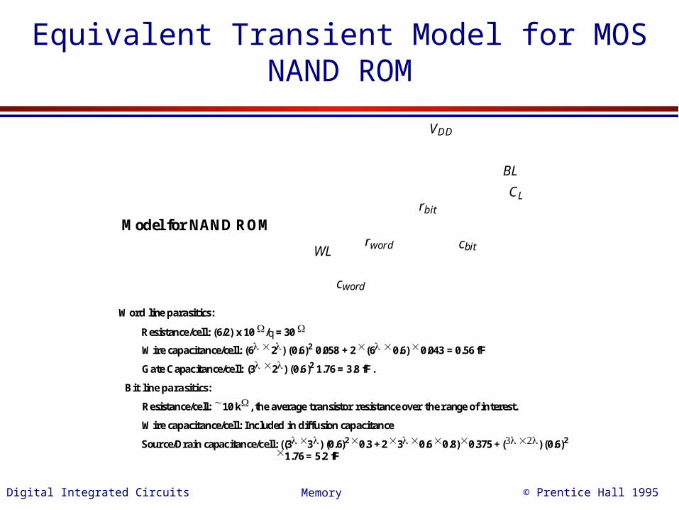
Equivalent Transient Model for MOS NAND ROM
VDD
WL
BL
rword
cword
CLrbit
cbit
Model for NAND ROM
Word line parasitics:
Resistance/cell: (6/2) x 10 /q = 30
Wire capacitance/cell: (6 2) (0.6)2 0.058 + 2 (6 0.6) 0.043 = 0.56 fF
Gate Capacitance/cell: (3 2) (0.6)2 1.76 = 3.8 fF.
Bit line parasitics:
Resistance/cell: 10 k, the average transistor resistance over the range of interest.
Wire capacitance/cell: Included in diffusion capacitance
Source/Drain capacitance/cell: ((3 3) (0.6)2 0.3 + 2 3 0.6 0.8) 0.375 + ( ) (0.6)2 1.76 = 5.2 fF
Digital Integrated Circuits © Prentice Hall 1995Memory
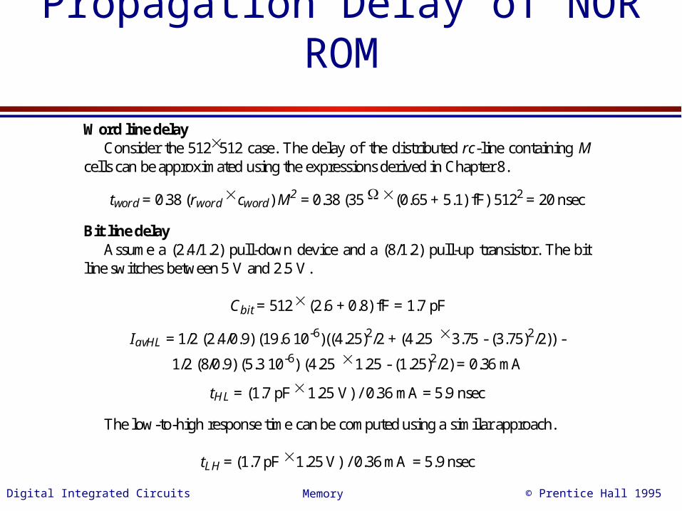
Propagation Delay of NOR ROM
Word line delayConsider the 512512 case. The delay of the distributed rc-line containing M
cells can be approximated using the expressions derived in Chapter 8.
tword = 0.38 (rword cword) M2 = 0.38 (35 (0.65 + 5.1) fF) 5122 = 20 nsec
Bit line delayAssume a (2.4/1.2) pull-down device and a (8/1.2) pull-up transistor. The bit
line switches between 5 V and 2.5 V.
Cbit = 512 (2.6 + 0.8) fF = 1.7 pF
IavHL = 1/2 (2.4/0.9) (19.6 10-6)((4.25)2/2 + (4.25 3.75 - (3.75)2/2)) -
1/2 (8/0.9) (5.3 10-6) (4.25 1.25 - (1.25)2/2) = 0.36 mA
tHL = (1.7 pF 1.25 V) / 0.36 mA = 5.9 nsec
The low-to-high response time can be computed using a similar approach.
tLH = (1.7 pF 1.25 V) / 0.36 mA = 5.9 nsec
Digital Integrated Circuits © Prentice Hall 1995Memory
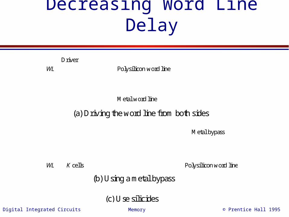
Decreasing Word Line Delay
Metal bypass
Polysilicon word lineK cells
Polysilicon word lineWL
Driver
(b) Using a metal bypass
(a) Driving the word line from both sides
Metal word line
WL
(c) Use silicides
Digital Integrated Circuits © Prentice Hall 1995Memory
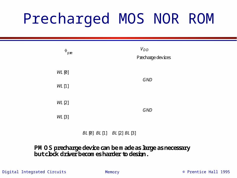
Precharged MOS NOR ROM
WL[0]
WL[1]
WL[2]
WL[3]
BL[0] BL[1] BL[2] BL[3]
GND
GND
VDD
Precharge devices
pre
PMOS precharge device can be made as large as necessary,but clock driver becomes harder to design.
Digital Integrated Circuits © Prentice Hall 1995Memory
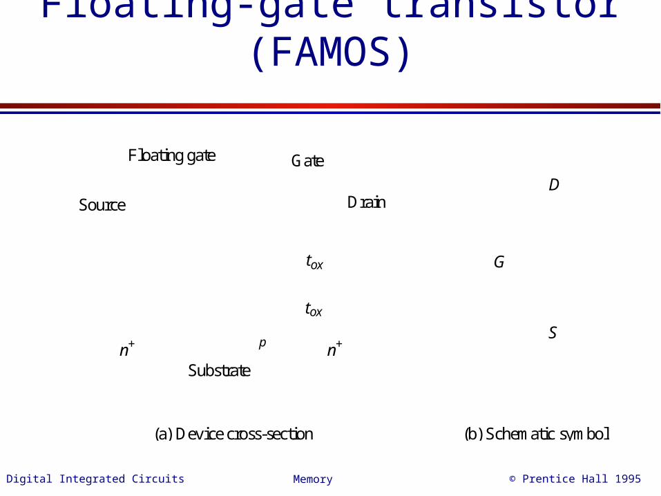
Floating-gate transistor (FAMOS)
Source Drain
GateFloating gate
tox
tox
Substraten+n+ p
(a) Device cross-section
S
D
G
(b) Schematic symbol
Digital Integrated Circuits © Prentice Hall 1995Memory
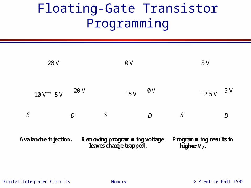
Floating-Gate Transistor Programming
DS
20 V
20 V
DS
0 V
0 V10 V 5 V 5 V
DS
5 V
5 V 2.5 V
Avalanche injection. Removing programming voltageleaves charge trapped.
Programming results inhigher VT.
Digital Integrated Circuits © Prentice Hall 1995Memory
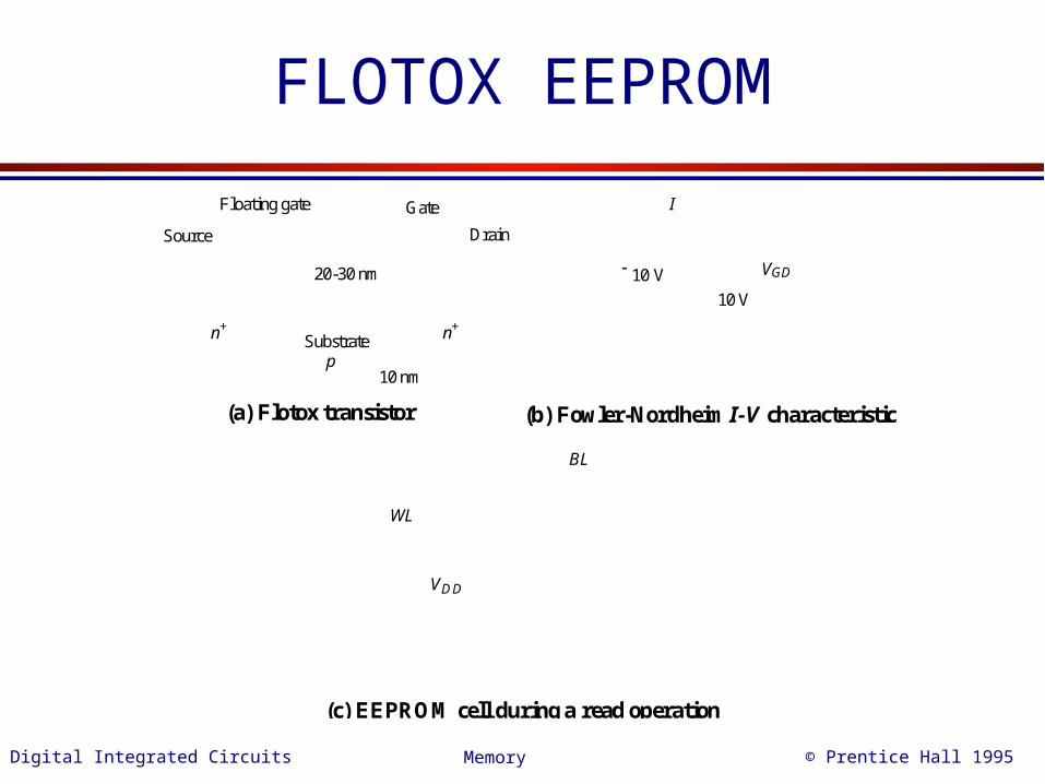
FLOTOX EEPROM
Source Drain
GateFloating gate
Substrate n+n+
10 nm
20-30 nm
(a) Flotox transistor
VGD
I
(b) Fowler-Nordheim I-V characteristic
10 V
10 V
p
BL
WL
VDD
(c) EEPROM cell during a read operation
Digital Integrated Circuits © Prentice Hall 1995Memory
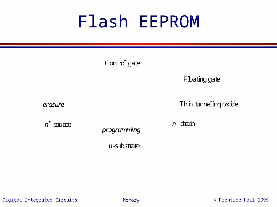
Flash EEPROM
n+ drainn+ source
p-substrate
Control gate
Floating gate
programming
erasure Thin tunneling oxide
Digital Integrated Circuits © Prentice Hall 1995Memory
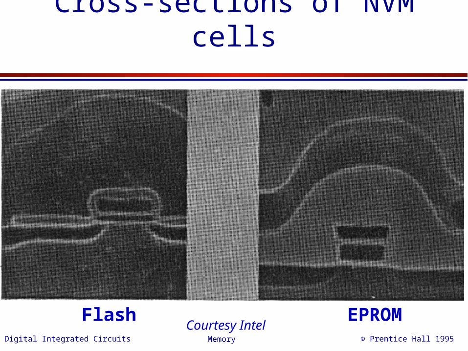
Cross-sections of NVM cells
EPROMFlashCourtesy Intel
Digital Integrated Circuits © Prentice Hall 1995Memory
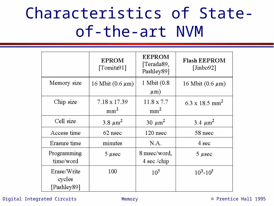
Characteristics of State-of-the-art NVM
Digital Integrated Circuits © Prentice Hall 1995Memory
Read-Write Memories (RAM)
• STATIC (SRAM)
• DYNAMIC (DRAM)
Data stored as long as supply is appliedLarge (6 transistors/cell)FastDifferential
Periodic refresh requiredSmall (1-3 transistors/cell)SlowerSingle Ended
Digital Integrated Circuits © Prentice Hall 1995Memory
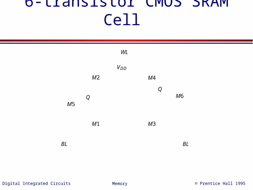
6-transistor CMOS SRAM Cell
VDD
Q
Q
M1 M3
M4M2
M5
BL
WL
BL
M6
Digital Integrated Circuits © Prentice Hall 1995Memory
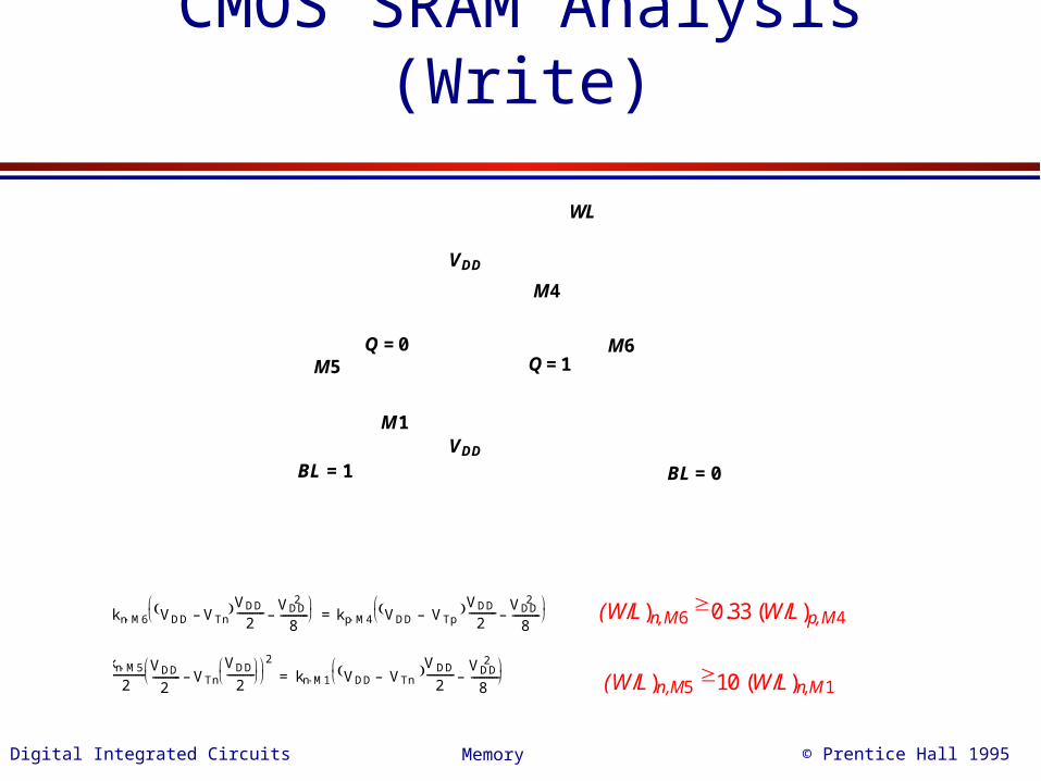
CMOS SRAM Analysis (Write)
VDD
Q = 1Q = 0
M1
M4
M5
BL = 1
WL
BL = 0
M6
VDD
kn M6 VDD VTn– VDD
2----------- VDD
2
8-----------–
kp M4 VDD VTp– VDD
2----------- VDD
2
8-----------–
=
kn M5
2--------------
VDD
2----------- VTn
VDD
2-----------
–
2
kn M1 VDD VTn– VDD
2-----------
VDD2
8-----------–
= (W/L)n,M510 (W/L)n,M1
(W/L)n,M60.33 (W/L)p,M4
Digital Integrated Circuits © Prentice Hall 1995Memory
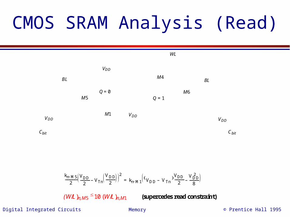
CMOS SRAM Analysis (Read)
VDD
Q = 1Q = 0
M1
M4
M5
BL
WL
BL
M6
VDDVDD
VDD
CbitCbit
kn M5
2---------------
VDD
2------------ VTn
VDD
2------------
–
2kn M1 VDD VTn–
VDD
2------------
VDD2
8------------–
=
(W/L)n,M510 (W/L)n,M1 (supercedes read constraint)
Digital Integrated Circuits © Prentice Hall 1995Memory
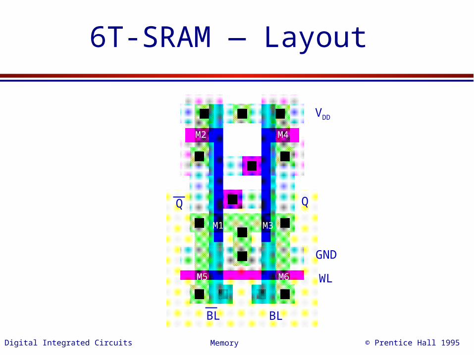
6T-SRAM — Layout
VDD
GND
WL
BLBL
M1 M3
M4M2
M5 M6
Digital Integrated Circuits © Prentice Hall 1995Memory
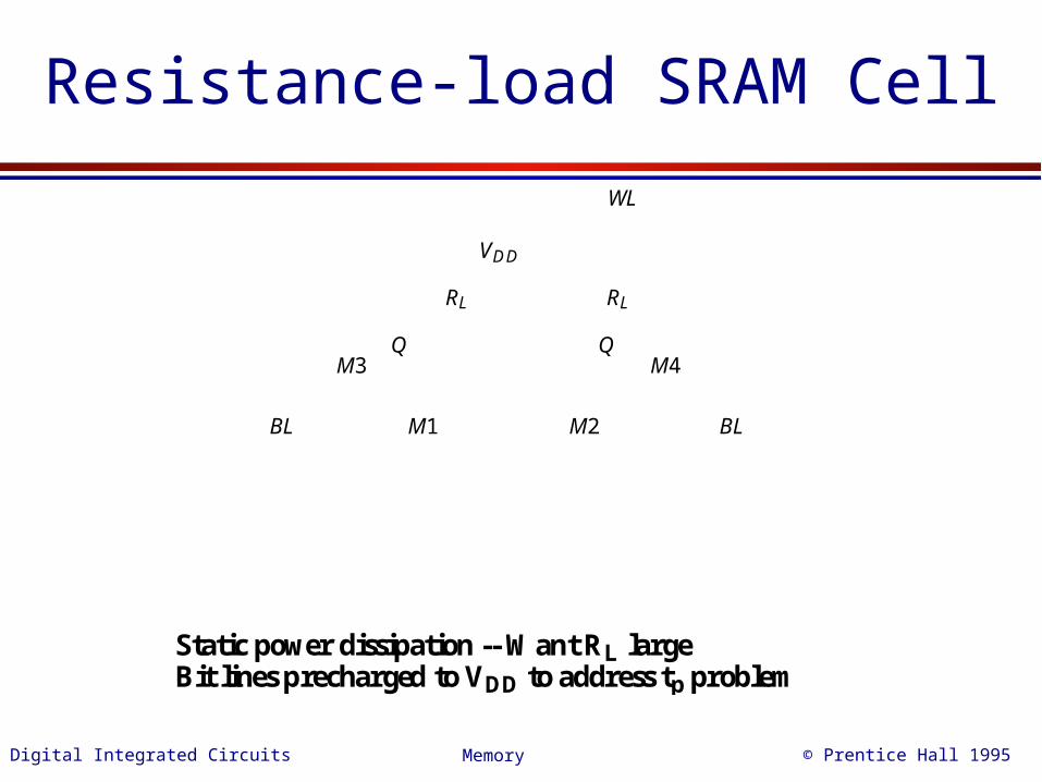
Resistance-load SRAM Cell
VDD
M1 M2
M3
BL
WL
BL
M4
RL RL
Static power dissipation -- Want RL largeBit lines precharged to VDD to address tp problem
Digital Integrated Circuits © Prentice Hall 1995Memory
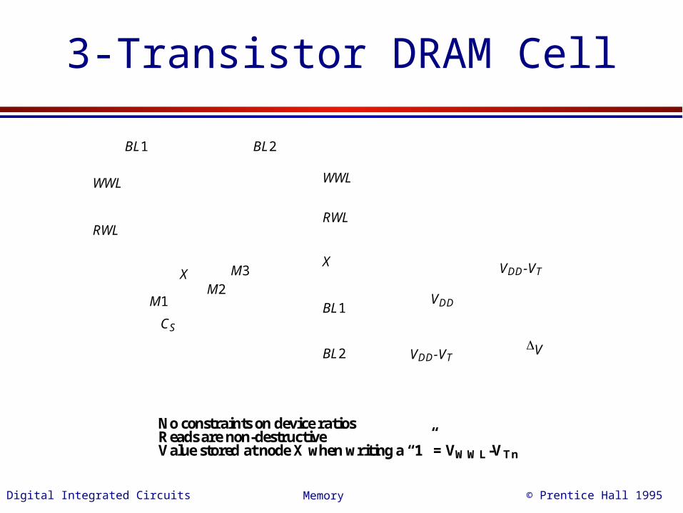
3-Transistor DRAM Cell
M2M1
BL1
WWL
BL2
M3
RWL
CS
X
WWL
RWL
X
BL1
BL2
VDD-VT
V
VDD
VDD-VT
No constraints on device ratiosReads are non-destructiveValue stored at node X when writing a “1” = VWWL-VTn
Digital Integrated Circuits © Prentice Hall 1995Memory
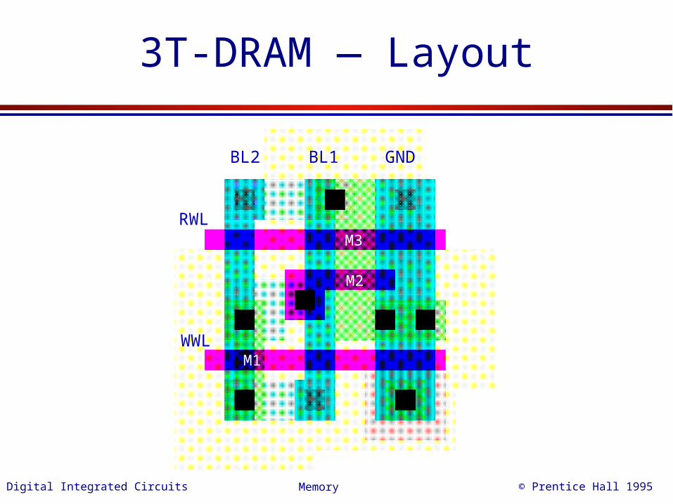
3T-DRAM — Layout
BL2 BL1 GND
RWL
WWL
M3
M2
M1
Digital Integrated Circuits © Prentice Hall 1995Memory
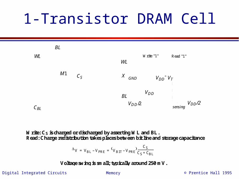
1-Transistor DRAM Cell
CSM1
BL
WL
CBL
WL
X
BL
VDD VT
VDD/2
VDD
GND
Write "1" Read "1"
sensingVDD/2
V VBL VPRE– VBIT VPRE– CS
CS CBL+------------------------= =
Write: CS is charged or discharged by asserting WL and BL.Read: Charge redistribution takes places between bit line and storage capacitance
Voltage swing is small; typically around 250 mV.
Digital Integrated Circuits © Prentice Hall 1995Memory
DRAM Cell Observations
1T DRAM requires a sense amplifier for each bit line, due to
charge redistribution read-out.
DRAM memory cells are single ended in contrast to SRAM cells.
The read-out of the 1T DRAM cell is destructive; read and
refresh operations are necessary for correct operation.
Unlike 3T cell, 1T cell requires presence of an extra capacitance
that must be explicitly included in the design.
When writing a “1” into a DRAM cell, a threshold voltage is lost.
This charge loss can be circumvented by bootstrapping the
word lines to a higher value than VDD.
Digital Integrated Circuits © Prentice Hall 1995Memory
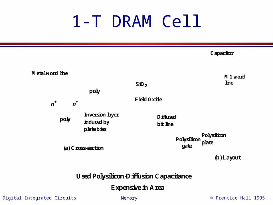
1-T DRAM Cell
(a) Cross-section
(b) Layout
Diffusedbit line
Polysiliconplate
M1 wordline
Capacitor
Polysilicongate
Metal word line
SiO2
n+ Field Oxide
Inversion layerinduced by plate bias
n+
poly
poly
Used Polysilicon-Diffusion Capacitance
Expensive in Area
Digital Integrated Circuits © Prentice Hall 1995Memory
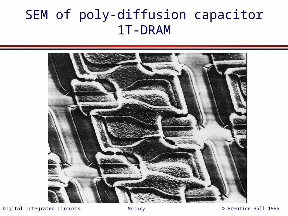
SEM of poly-diffusion capacitor 1T-DRAM
Digital Integrated Circuits © Prentice Hall 1995Memory
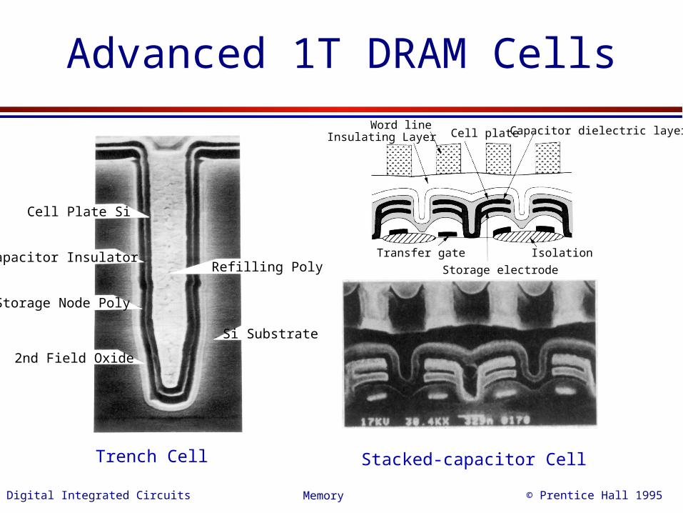
Advanced 1T DRAM Cells
Cell Plate Si
Capacitor Insulator
Storage Node Poly
2nd Field Oxide
Refilling Poly
Si Substrate
Trench Cell Stacked-capacitor Cell
Capacitor dielectric layerCell plateWord line
Insulating Layer
IsolationTransfer gate
Storage electrode
Digital Integrated Circuits © Prentice Hall 1995Memory
Periphery
• Decoders
• Sense Amplifiers
• Input/Output Buffers
• Control / Timing Circuitry
Digital Integrated Circuits © Prentice Hall 1995Memory
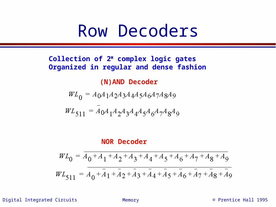
Row DecodersCollection of 2M complex logic gatesOrganized in regular and dense fashion
(N)AND Decoder
NOR Decoder
Digital Integrated Circuits © Prentice Hall 1995Memory
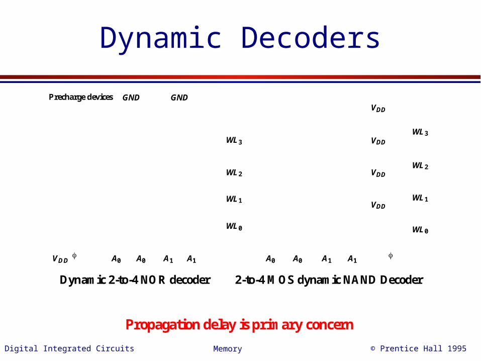
Dynamic Decoders
WL3
GND GNDPrecharge devices
WL2
WL1
WL0
VDD A0 A0 A1 A1 A0 A0 A1 A1
VDD
VDD
VDD
VDD
WL3
WL2
WL1
WL0
Dynamic 2-to-4 NOR decoder 2-to-4 MOS dynamic NAND Decoder
Propagation delay is primary concern
Digital Integrated Circuits © Prentice Hall 1995Memory
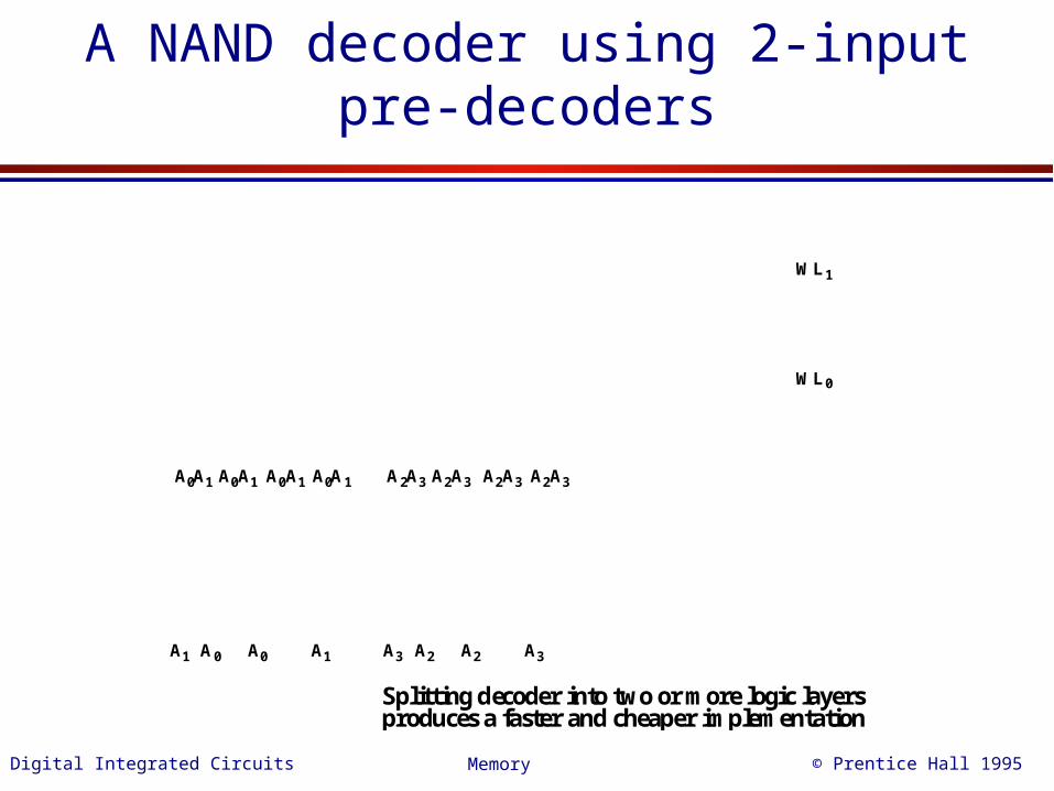
A NAND decoder using 2-input pre-decoders
A0A1 A0A1 A0A1 A0A1 A2A3 A2A3 A2A3 A2A3
A1 A0 A0 A1 A3 A2 A2 A3
WL0
WL1
Splitting decoder into two or more logic layersproduces a faster and cheaper implementation
Digital Integrated Circuits © Prentice Hall 1995Memory
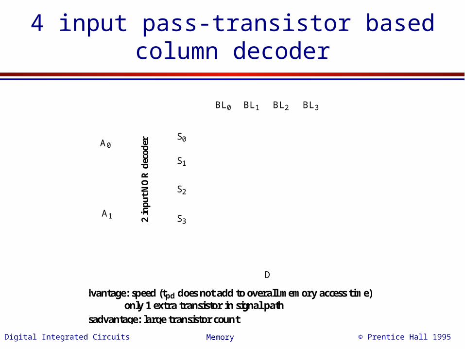
4 input pass-transistor based column decoder
BL0 BL1 BL2 BL3
D
A0
A1
S0
S1
S2
S3 2 i
npu
t NO
R d
ecod
er
Advantage: speed (tpd does not add to overall memory access time)
Disadvantage: large transistor countonly 1 extra transistor in signal path
Digital Integrated Circuits © Prentice Hall 1995Memory
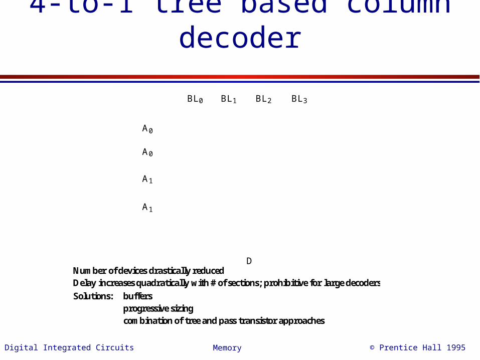
4-to-1 tree based column decoder
BL0 BL1 BL2 BL3
D
A0
A0
A1
A1
Number of devices drastically reducedDelay increases quadratically with # of sections; prohibitive for large decoders
buffersprogressive sizingcombination of tree and pass transistor approaches
Solutions:
Digital Integrated Circuits © Prentice Hall 1995Memory
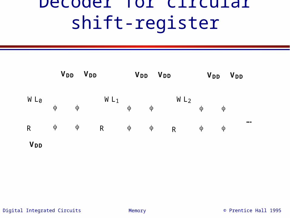
Decoder for circular shift-register
VDDVDD
VDDVDD
VDDVDD
RRR
VDD
...
WL0 WL1 WL2
Digital Integrated Circuits © Prentice Hall 1995Memory
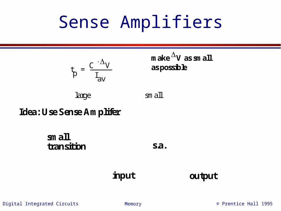
Sense Amplifiers
tpC V
Iav----------------=
make V as smallas possible
smalllarge
Idea: Use Sense Amplifer
outputinput
s.a.smalltransition
Digital Integrated Circuits © Prentice Hall 1995Memory
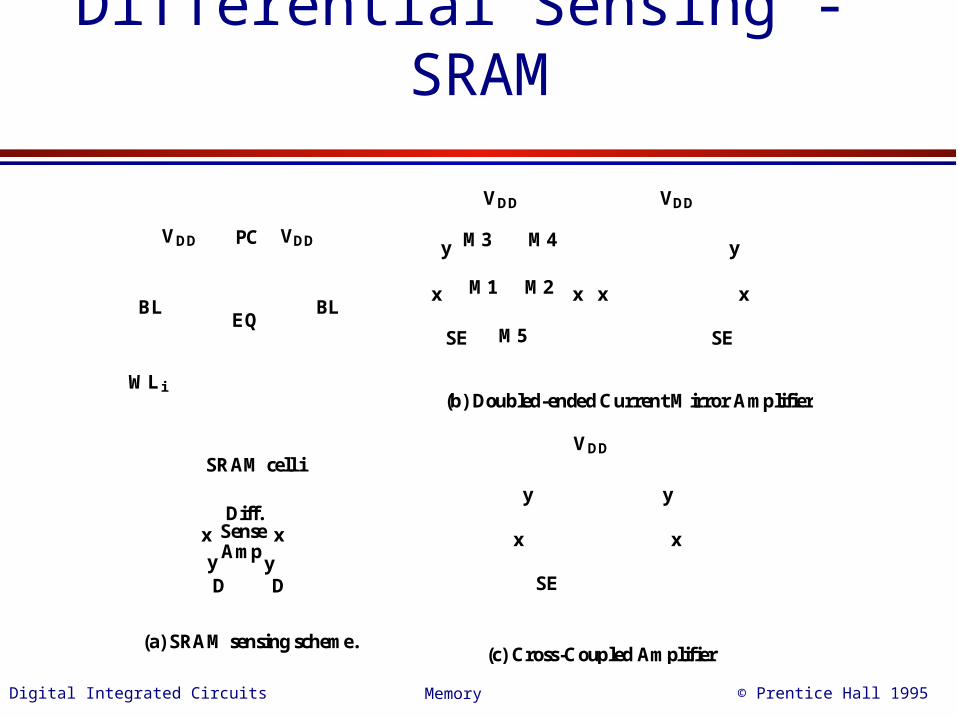
Differential Sensing - SRAM
Diff.SenseAmp
BLBL
SRAM cell i
x x
y yD D
VDDVDD
WLi
PC
EQ
VDD
x x
y
SE
VDD
xx
y
SE
VDD
x x
y
SE
(b) Doubled-ended Current Mirror Amplifier
y
(a) SRAM sensing scheme.(c) Cross-Coupled Amplifier
M1 M2
M4M3
M5
Digital Integrated Circuits © Prentice Hall 1995Memory
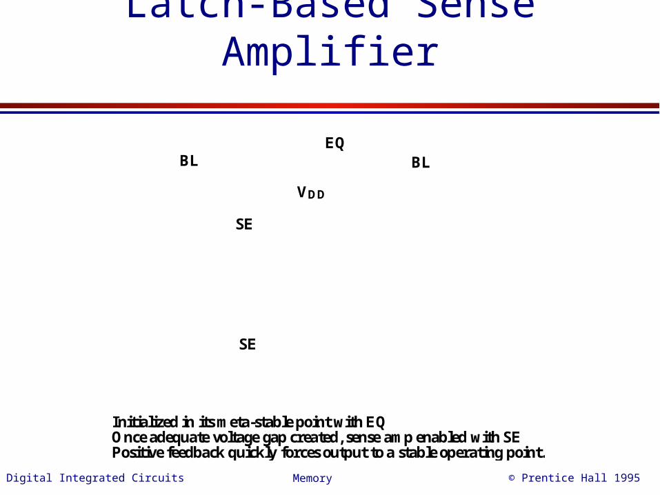
Latch-Based Sense Amplifier
VDD
BL
SE
SE
BLEQ
Initialized in its meta-stable point with EQOnce adequate voltage gap created, sense amp enabled with SEPositive feedback quickly forces output to a stable operating point.
Digital Integrated Circuits © Prentice Hall 1995Memory
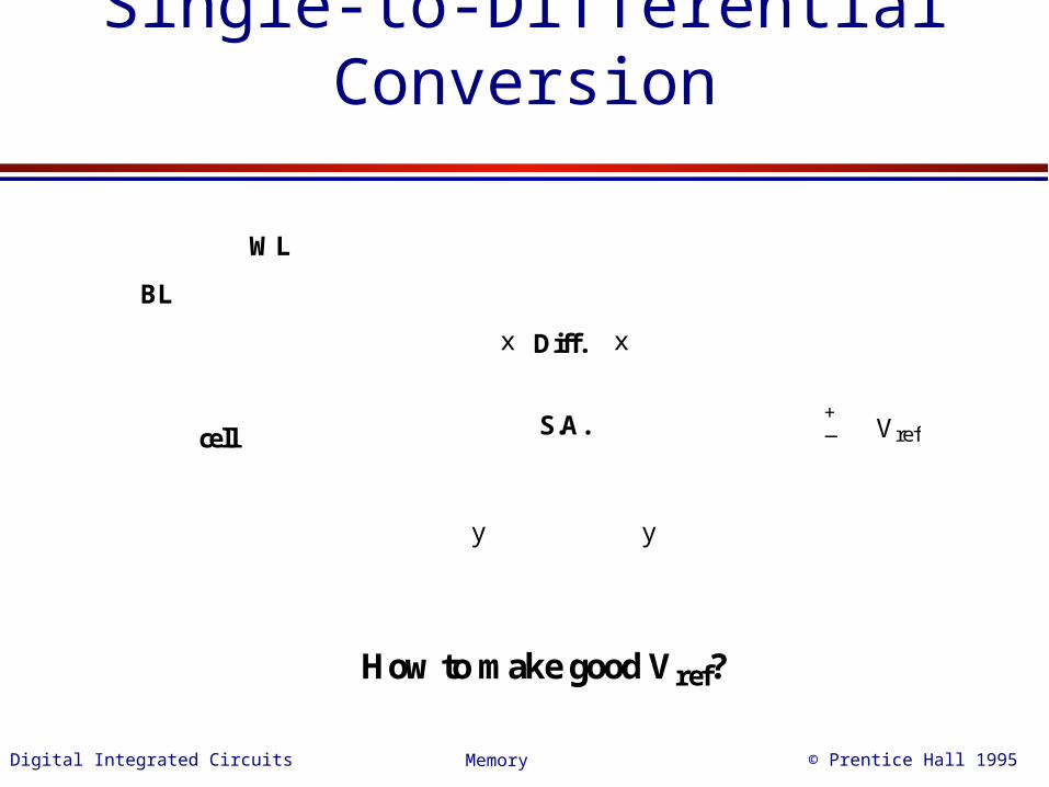
Single-to-Differential Conversion
Diff.
S.A.cell
BL
Vref+_
WL
x x
y y
How to make good Vref?
Digital Integrated Circuits © Prentice Hall 1995Memory
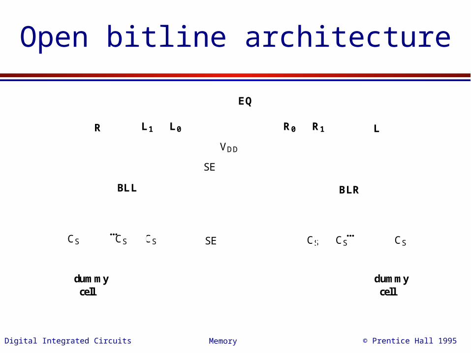
Open bitline architecture
VDD
SE
SE
CS CS CS
L
...CSCS
...CS
R
BLL BLR
L0L1 R0 R1
dummycell
dummycell
EQ
Digital Integrated Circuits © Prentice Hall 1995Memory
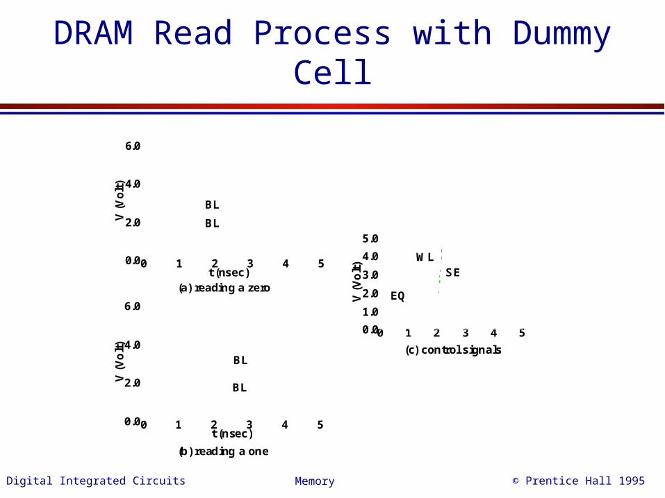
DRAM Read Process with Dummy Cell
0 1 2 3 4 5t (nsec)
0.0
2.0
4.0
6.0
V (
Vo
lt)
0 1 2 3 4 5t (nsec)
0.0
2.0
4.0
6.0
V (
Vo
lt)
0 1 2 3 4 50.0
1.0
2.0
3.0
4.0
5.0
V (
Vo
lt)
EQ
WLSE
BL
BL
BL
BL
(a) reading a zero
(b) reading a one
(c) control signals
Digital Integrated Circuits © Prentice Hall 1995Memory
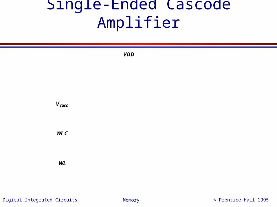
Single-Ended Cascode Amplifier
VDD
WL
WLC
Vcasc
Digital Integrated Circuits © Prentice Hall 1995Memory
DRAM Timing
Digital Integrated Circuits © Prentice Hall 1995Memory
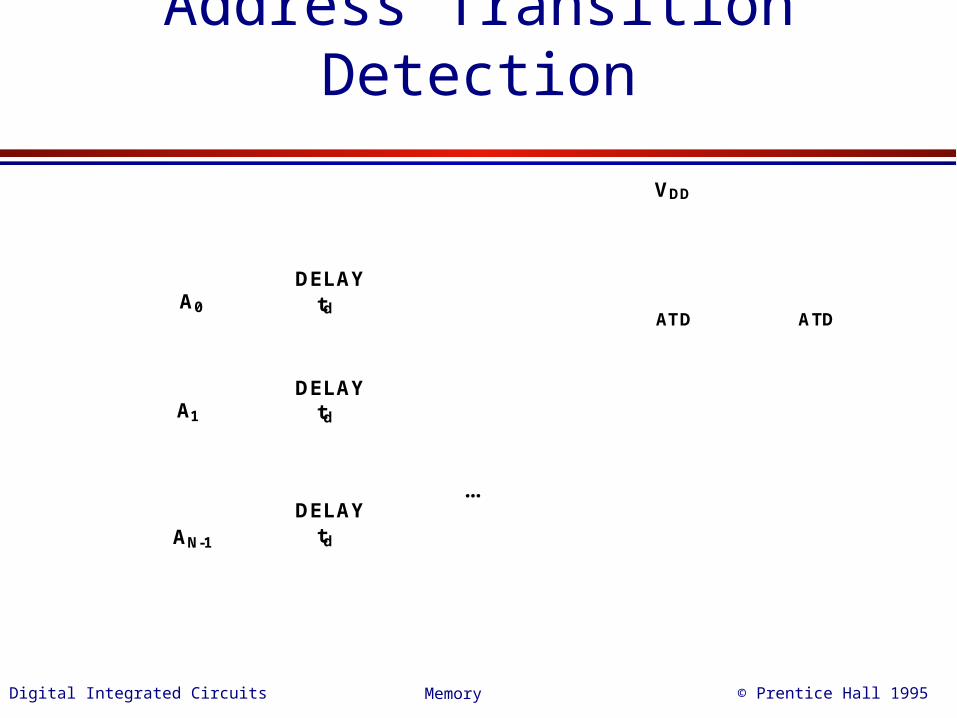
Address Transition Detection
DELAYtdA0
DELAYtd
DELAYtd
ATD
...
A1
AN-1
VDD
ATD
Digital Integrated Circuits © Prentice Hall 1995Memory
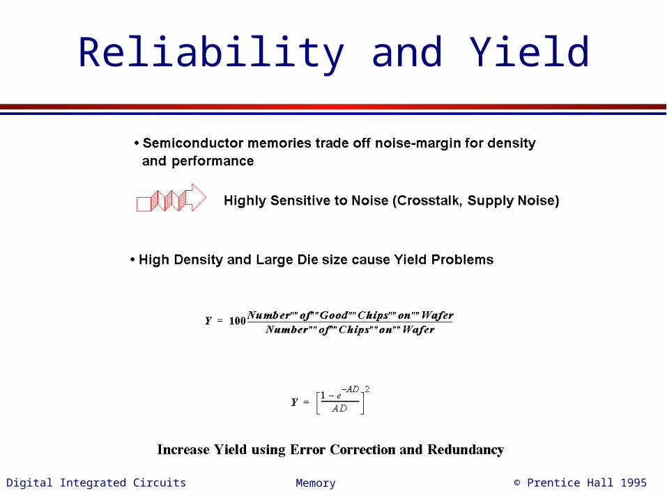
Reliability and Yield
Digital Integrated Circuits © Prentice Hall 1995Memory
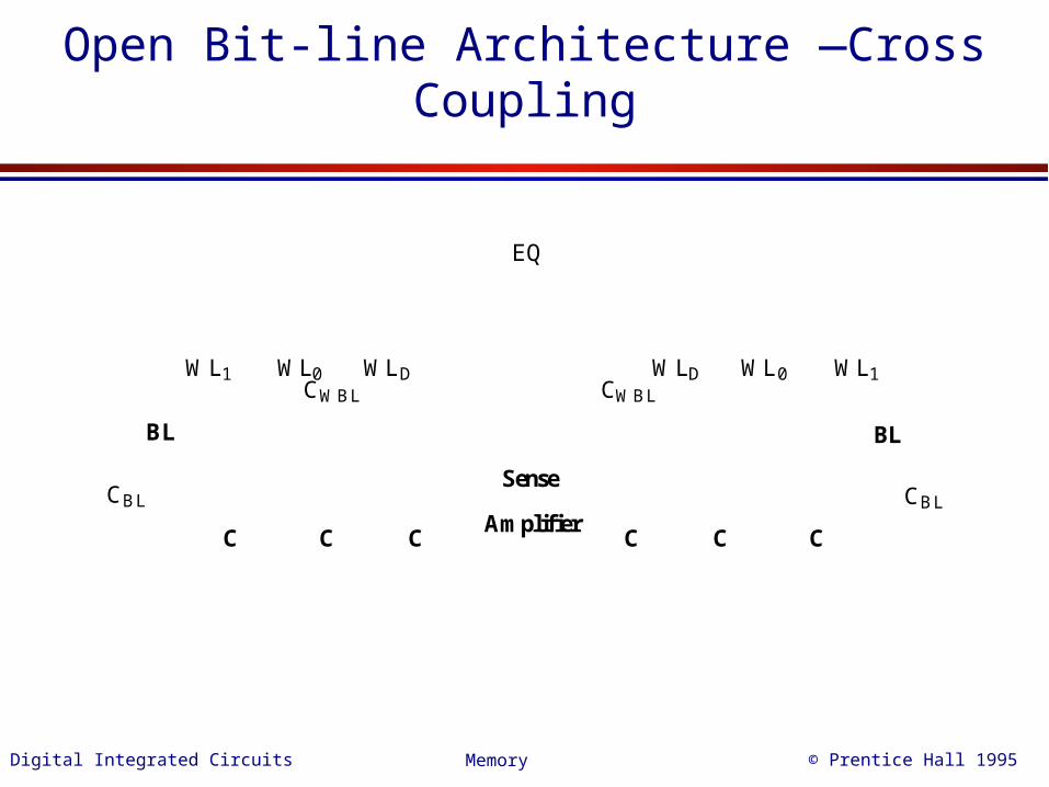
Open Bit-line Architecture —Cross Coupling
Sense
AmplifierC C CCCC
WL1 WL0 WLD WLD WL0 WL1
EQ
CWBLCWBL
CBL
BL
CBL
BL
Digital Integrated Circuits © Prentice Hall 1995Memory
Folded-Bitline Architecture
BL
...
WLDWLD
BL
y
yx
x
WL0
CCCCCCEQ
Sense
Amplifier
WL0WL1WL1
CBL
CBL
CWBL
CWBL
Digital Integrated Circuits © Prentice Hall 1995Memory
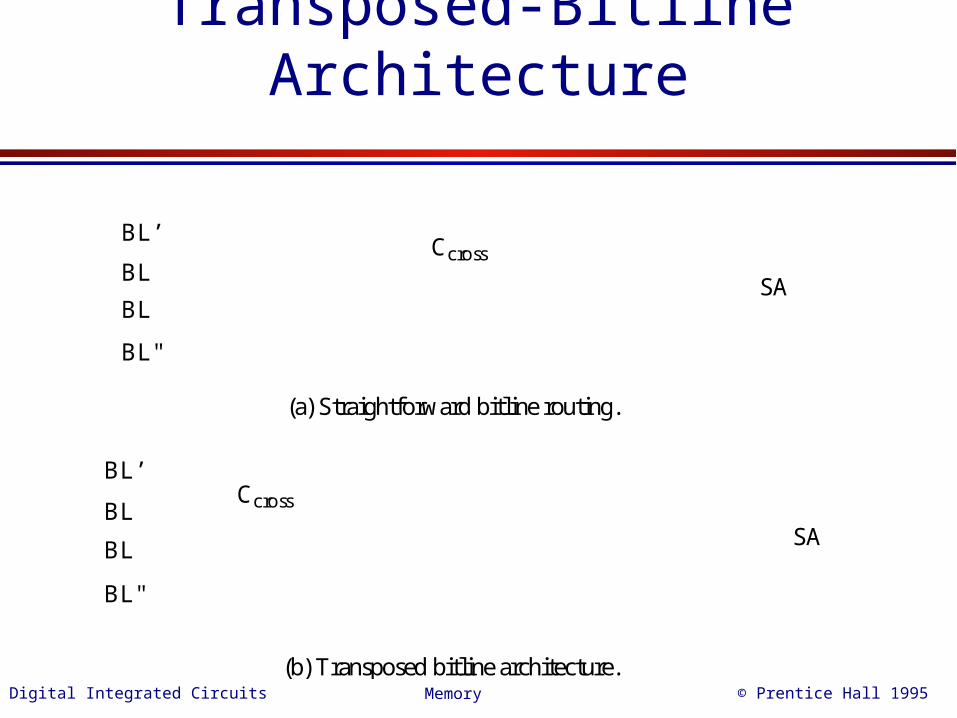
Transposed-Bitline Architecture
BL
BL
BL’
BL"
SA
Ccross
SABL
BL
BL’
BL"
Ccross
(a) Straightforward bitline routing.
(b) Transposed bitline architecture.
Digital Integrated Circuits © Prentice Hall 1995Memory
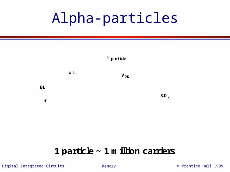
Alpha-particles
WL
BL
VDD
n+SiO2
-particle
1 particle ~ 1 million carriers
Digital Integrated Circuits © Prentice Hall 1995Memory
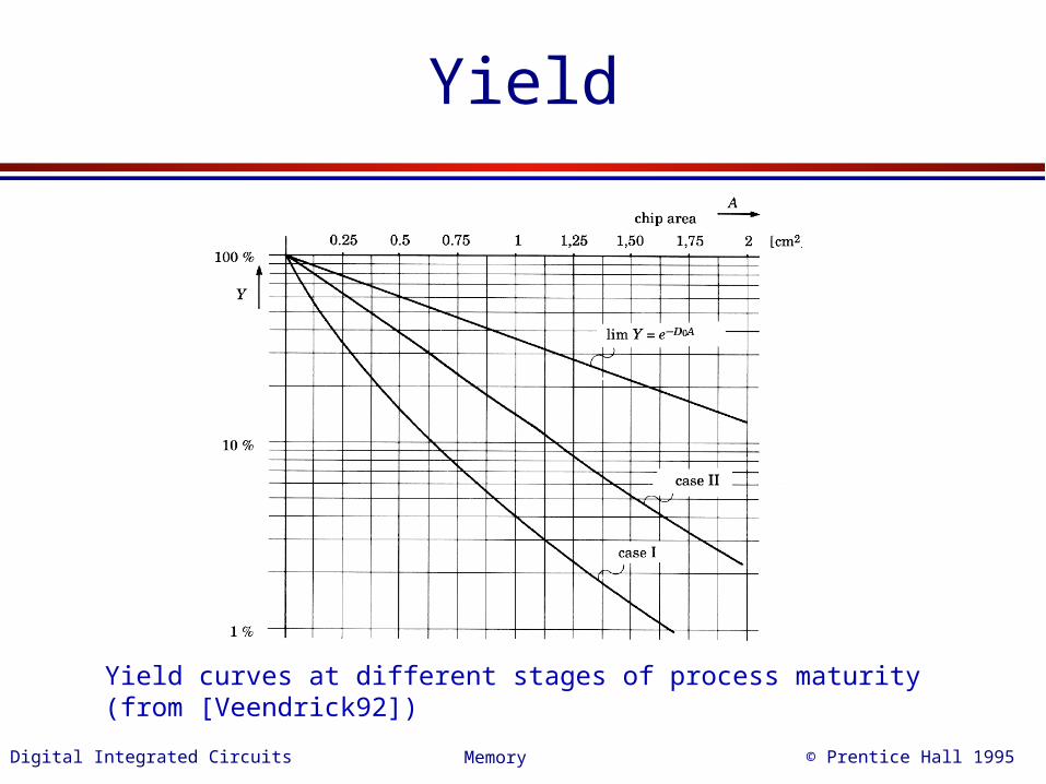
Yield
Yield curves at different stages of process maturity(from [Veendrick92])
Digital Integrated Circuits © Prentice Hall 1995Memory
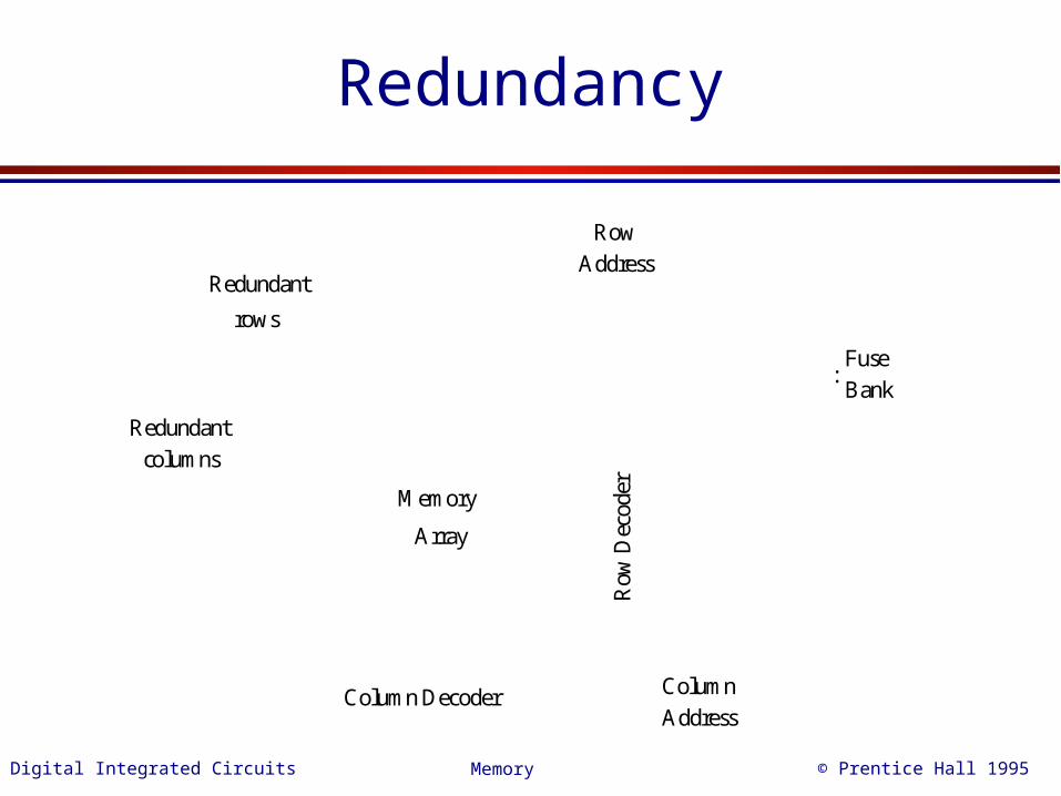
Redundancy
Memory
Array
Redundant
columns
Redundant
rows
Column Decoder
Row
Dec
oder
Row
Address
Column
Address
Fuse
Bank:
Digital Integrated Circuits © Prentice Hall 1995Memory
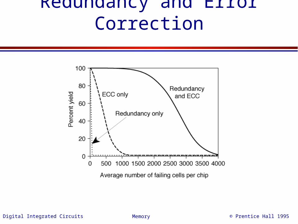
Redundancy and Error Correction
Digital Integrated Circuits © Prentice Hall 1995Memory
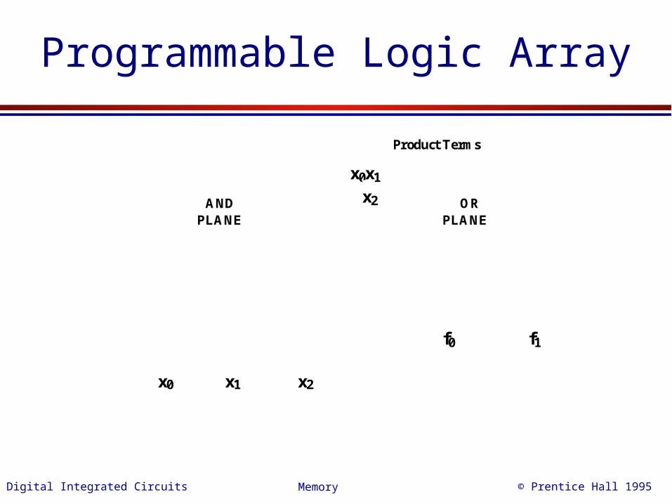
Programmable Logic Array
x0 x1 x2
f0 f1
ANDPLANE
ORPLANE
x0x1
x2
Product Terms
Digital Integrated Circuits © Prentice Hall 1995Memory
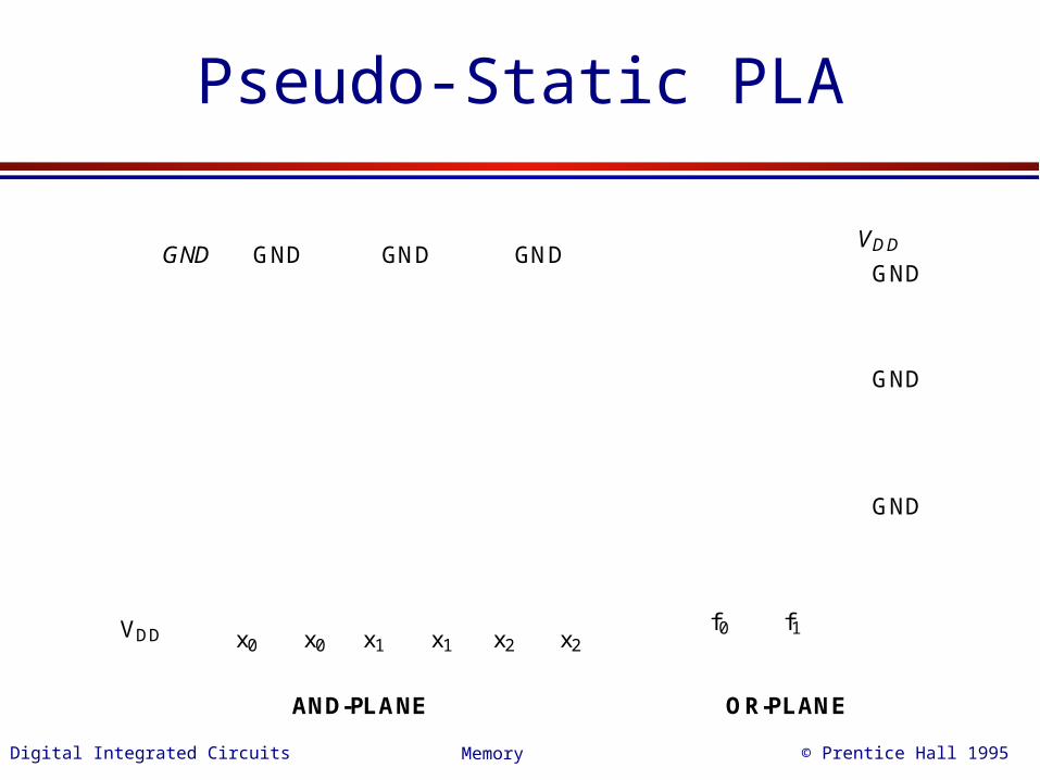
Pseudo-Static PLA
f0 f1
GND
GND
VDD
GND
x0 x0 x1 x1 x2 x2
GND GND GND GND
VDD
AND-PLANE OR-PLANE
Digital Integrated Circuits © Prentice Hall 1995Memory
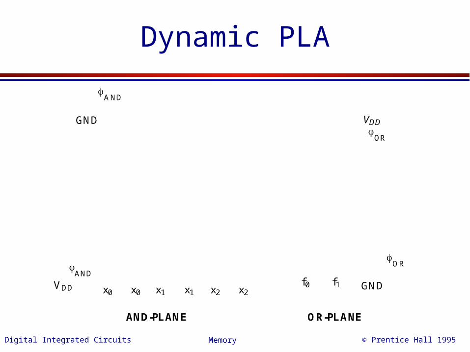
Dynamic PLA
f0 f1 GND
VDD
OR
x0 x0 x1 x1 x2 x2
GND
VDD
AND-PLANE OR-PLANE
AND
OR
AND
Digital Integrated Circuits © Prentice Hall 1995Memory
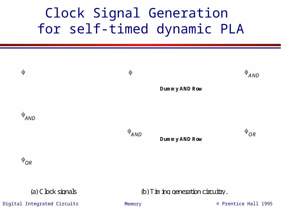
Clock Signal Generation for self-timed dynamic PLA
AND
OR
AND
Dummy AND Row
ANDDummy AND Row
OR
(a) Clock signals (b) Timing generation circuitry.
Digital Integrated Circuits © Prentice Hall 1995Memory
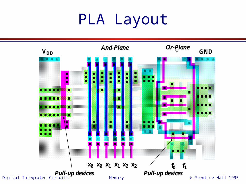
PLA Layout
VDD GNDAnd-Plane Or-Plane
f0 f1x0 x0 x1 x1 x2 x2
Pull-up devices Pull-up devices
Digital Integrated Circuits © Prentice Hall 1995Memory
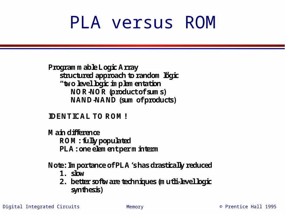
PLA versus ROM
Programmable Logic Arraystructured approach to random logic“two level logic implementation”
NOR-NOR (product of sums)NAND-NAND (sum of products)
IDENTICAL TO ROM!
Main differenceROM: fully populatedPLA: one element per minterm
Note: Importance of PLA’s has drastically reduced1. slow2. better software techniques (mutli-level logic
synthesis)
Digital Integrated Circuits © Prentice Hall 1995Memory
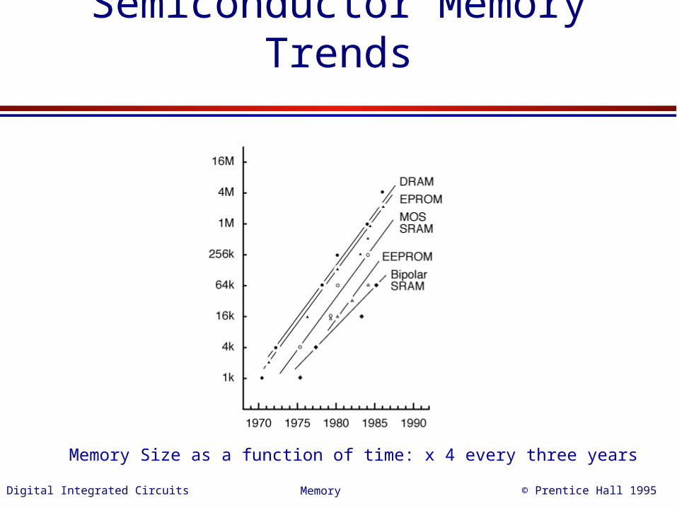
Semiconductor Memory Trends
Memory Size as a function of time: x 4 every three years
Digital Integrated Circuits © Prentice Hall 1995Memory
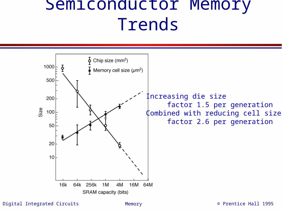
Semiconductor Memory Trends
Increasing die size factor 1.5 per generationCombined with reducing cell size factor 2.6 per generation
Digital Integrated Circuits © Prentice Hall 1995Memory
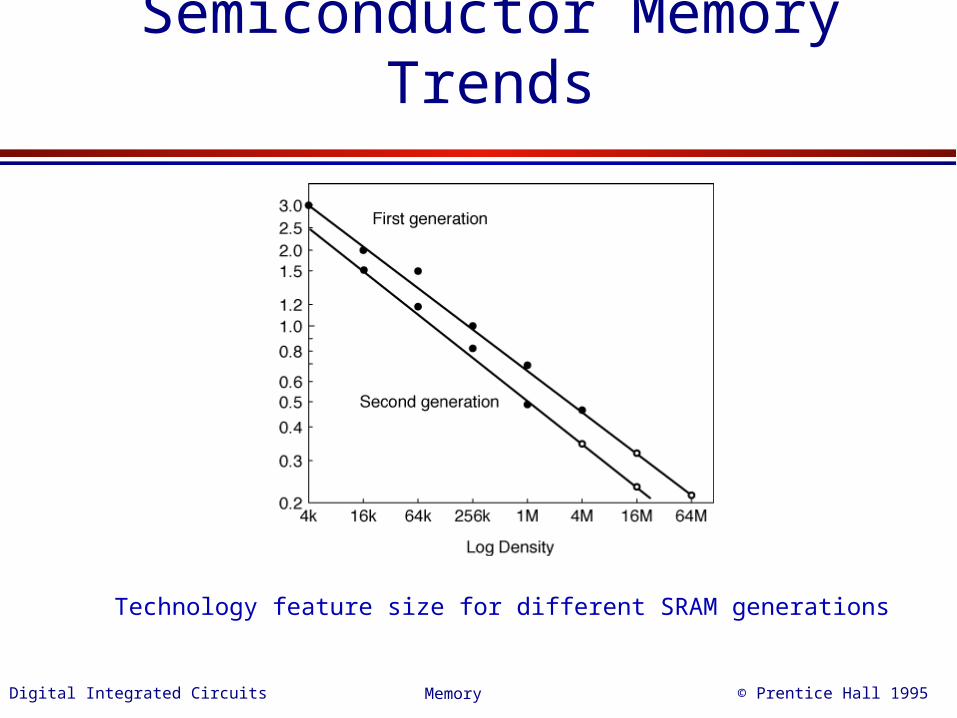
Semiconductor Memory Trends
Technology feature size for different SRAM generations