Embed Size (px)
Citation preview
Investigation of Performance Issues Affecting Optical Circuit and Packet
Switched WDM Networks
A THESIS SUBMITTED FOR THE DEGREE OF DOCTOR OF PHILOSOPHY
To
Dublin City University
By
Frank Smyth, B.Eng, M.Eng
School of Electronic Engineering
Faculty of Engineering and Computing
Dublin City University
August 2008
Supervised by:
Professor Liam Barry

ii
Approval
Candidate: Frank Smyth
Degree: Doctor of Philosophy
Thesis Title: Investigation of Performance Issues affecting Optical Circuit
and Packet Switched WDM Networks
Examining Committee: Chairperson: ____________________________
External Examiner: ____________________________
Prof. Antonio Teixeira
Internal Examiner: ____________________________
Dr. Martin Collier
Supervisor: ____________________________
Prof. Liam Barry

iii
Declaration I hereby certify that this material, which I now submit for assessment on the programme of
study leading to the award of Doctor of Philosophy is entirely my own work, that I have
exercised reasonable care to ensure that the work is original, and does not to the best of my
knowledge breach any law of copyright, and has not been taken from the work of others
save and to the extent that such work has been cited and acknowledged within the text of my
work.
Signed: _________________________________
ID No.: _________________________________
Date: _________________________________

iv
Dedicated to Nic

v
Acknowledgements
I would like to thank my supervisor, Professor Liam Barry, for his initial faith in my ability,
and for the support and guidance that he has given me throughout this PhD.
I am indebted to my colleagues past and present, for the role they have played, both
academically and socially, in my time with the Radio and Optical Communications Group.
The researchers that I have collaborated with while working towards this PhD also deserve
my gratitude, especially my mentor in Bell Labs, Dr. Dan Kilper.
Finally, I would like to thank my parents for their support, and my fiancée Nicola, for her
initial encouragement of, and subsequent patience with my ‘eternal’ studentship.
vi
Abstract Optical switching represents the next step in the evolution of optical networks. This thesis
describes work that was carried out to examine performance issues which can occur in two
distinct varieties of optical switching networks.
Slow optical switching in which lightpaths are requested, provisioned and torn down when
no longer required is known as optical circuit switching (OCS). Services enabled by OCS
include wavelength routing, dynamic bandwidth allocation and protection switching. With
network elements such as reconfigurable optical add/drop multiplexers (ROADMs) and
optical cross connects (OXCs) now being deployed along with the generalized multi-
protocol label switching (GMPLS) control plane this represents the current state of the art in
commercial networks. These networks often employ erbium doped fiber amplifiers (EDFAs)
to boost the optical signal to noise ratio of the WDM channels and as channel configurations
change, wavelength dependent gain variations in the EDFAs can lead to channel power
divergence that can result in significant performance degradation. This issue is examined in
detail using a reconfigurable wavelength division multiplexed (WDM) network testbed and
results show the severe impact that channel reconfiguration can have on transmission
performance.
Following the slow switching work the focus shifts to one of the key enabling technologies
for fast optical switching, namely the tunable laser. Tunable lasers which can switch on the
nanosecond timescale will be required in the transmitters and wavelength converters of
optical packet switching networks. The switching times and frequency drifts, both of
commercially available lasers, and of novel devices are investigated and performance issues
which can arise due to this frequency drift are examined. An optical packet switching
transmitter based on a novel label switching technique and employing one of the fast tunable
lasers is designed and employed in a dual channel WDM packet switching system. In depth
performance evaluations of this labelling scheme and packet switching system show the
detrimental impact that wavelength drift can have on such systems.
vii
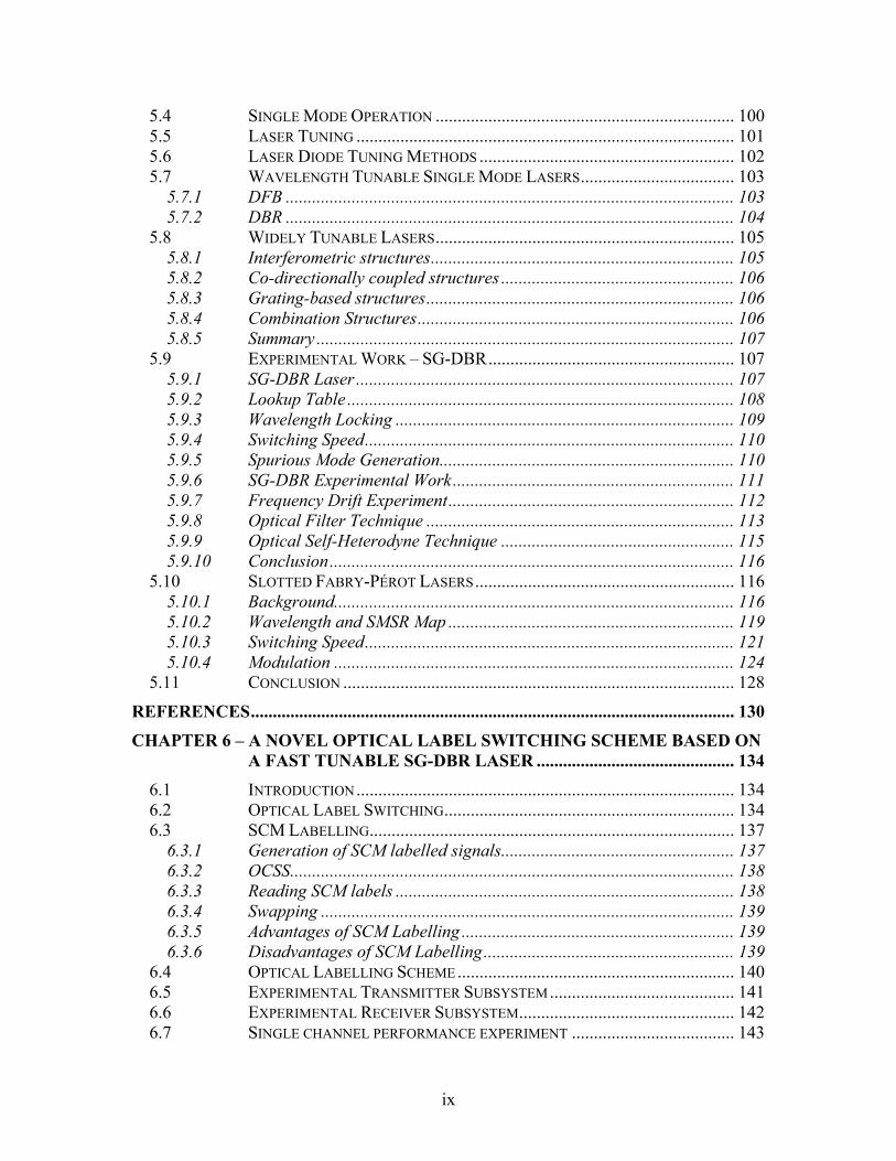
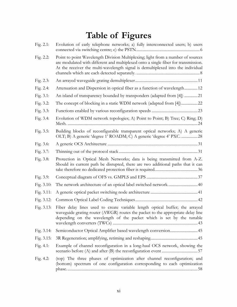
Table of Contents Approval.............................................................................................................................. ii Declaration ........................................................................................................................ iii Acknowledgements...............................................................................................................v Abstract ...............................................................................................................................vi Table of Contents .............................................................................................................. vii Table of Figures..................................................................................................................xi List of Acronyms ..............................................................................................................xvii
CHAPTER 1 – INTRODUCTION.................................................................................. 1
REFERENCES.................................................................................................................. 5
CHAPTER 2 – OPTICAL NETWORKS AND WAVELENGTH DIVISION MULTIPLEXING .................................................................................. 6
2.1 OPTICAL NETWORKS – A BRIEF HISTORY ................................................. 6 2.2 OPTICAL MULTIPLEXING ........................................................................... 7 2.3 WAVELENGTH DIVISION MULTIPLEXING................................................... 8 2.4 CLASSIFICATION OF WDM SYSTEMS ........................................................ 9 2.5 MAJOR OPTICAL COMPONENTS OF A DWDM NETWORK........................... 9
2.5.1 Light Sources ............................................................................................ 9 2.5.2 Modulators ............................................................................................. 10 2.5.3 Multiplexers/Demultiplexers .................................................................. 10 2.5.4 Fiber ....................................................................................................... 12 2.5.5 Amplifiers ............................................................................................... 13 2.5.6 Photoreceivers........................................................................................ 15
2.6 CONCLUSION AND PERSPECTIVE.............................................................. 15
REFERENCES................................................................................................................ 17
CHAPTER 3 – RECONFIGURATION IN WDM NETWORKS AND OPTICAL SWITCHING ........................................................................................ 20
3.1 INTRODUCTION........................................................................................ 20 3.2 TRANSPARENCY ...................................................................................... 20 3.3 RECONFIGURABILITY............................................................................... 22 3.4 EVOLUTION OF OPTICAL NETWORK TOPOLOGIES.................................... 23 3.5 OPTICAL SWITCHING TECHNOLOGIES...................................................... 24 3.6 ELEMENTS OF AN OPTICAL SWITCHING NETWORK.................................. 26
3.6.1 Optical Line Terminals........................................................................... 27 3.6.2 ROADMs................................................................................................. 27 3.6.3 Cross Connects....................................................................................... 29
3.7 OPTICAL CIRCUIT SWITCHING ................................................................. 30 3.7.1 Network Architecture.............................................................................. 31 3.7.2 Control Plane ......................................................................................... 32 3.7.3 Applications............................................................................................ 35 3.7.4 OCS versus other Optical Switching Techniques................................... 36
3.8 OPTICAL IP SWITCHING........................................................................... 36
viii
3.9 OPTICAL FLOW SWITCHING..................................................................... 37 3.10 OPTICAL BURST SWITCHING.................................................................... 38 3.11 OPTICAL PACKET SWITCHING.................................................................. 39
3.11.1 Optical Label Switching ......................................................................... 40 3.11.2 Technology to Enable Optical Packet Switching ................................... 42
3.12 CONCLUSION ........................................................................................... 46
REFERENCES................................................................................................................ 47
CHAPTER 4 – THE PERFORMANCE IMPACT OF RECONFIGURATION IN OPTICAL CIRCUIT SWITCHED NETWORKS............................ 56
4.1 RECONFIGURATION IN LONG-HAUL TRANSPARENT NETWORKS................ 56 4.2 EDFAS IN LONG HAUL NETWORKS .......................................................... 59
4.2.1 EDFA Noise and OSNR.......................................................................... 60 4.2.2 EDFA gain flatness and the effect on OSNR.......................................... 61 4.2.3 Transient gain dynamics......................................................................... 62 4.2.4 Steady state gain dynamics..................................................................... 63
4.3 TRANSMISSION IMPAIRMENTS IN LONG HAUL NETWORKS...................... 64 4.3.1 Dispersion............................................................................................... 64 4.3.2 Nonlinearities ......................................................................................... 66 4.3.3 Linear crosstalk ...................................................................................... 70 4.3.4 Polarization Effects ................................................................................ 71
4.4 CIRCULATING LOOPS............................................................................... 72 4.5 EXPERIMENT............................................................................................ 74
4.5.1 Setup ....................................................................................................... 74 4.5.2 Channel Configurations ......................................................................... 75 4.5.3 Experimental Process............................................................................. 76 4.5.4 Channel Launch Powers and Dispersion Maps ..................................... 80
4.6 EXPERIMENTAL RESULTS ........................................................................ 81 4.6.1 Power Evolution ..................................................................................... 81 4.6.2 Performance ........................................................................................... 83 4.6.3 Comparison of different launch powers and dispersion maps ............... 87
4.7 CONCLUSION ........................................................................................... 89
REFERENCES................................................................................................................ 91
CHAPTER 5 – CHARACTERIZATION OF TUNABLE LASERS FOR USE IN RECONFIGURABLE OPTICAL NETWORKS .............................. 95
5.1 TUNABLE LASERS - APPLICATIONS.......................................................... 95 5.1.1 Inventory Reduction................................................................................ 95 5.1.2 Reconfiguration ...................................................................................... 96
5.2 TUNABLE LASERS – REQUIREMENTS ....................................................... 97 5.2.1 Single Mode Operation: ......................................................................... 97 5.2.2 Tuning Range: ........................................................................................ 97 5.2.3 Tuning Continuity................................................................................... 97 5.2.4 Tuning Speed .......................................................................................... 98 5.2.5 Tuning Accuracy and Stability ............................................................... 99
5.3 SEMICONDUCTOR LASER BACKGROUND ................................................. 99
ix
5.4 SINGLE MODE OPERATION .................................................................... 100 5.5 LASER TUNING ...................................................................................... 101 5.6 LASER DIODE TUNING METHODS .......................................................... 102 5.7 WAVELENGTH TUNABLE SINGLE MODE LASERS................................... 103
5.7.1 DFB ...................................................................................................... 103 5.7.2 DBR ...................................................................................................... 104
5.8 WIDELY TUNABLE LASERS.................................................................... 105 5.8.1 Interferometric structures..................................................................... 105 5.8.2 Co-directionally coupled structures ..................................................... 106 5.8.3 Grating-based structures...................................................................... 106 5.8.4 Combination Structures........................................................................ 106 5.8.5 Summary ............................................................................................... 107
5.9 EXPERIMENTAL WORK – SG-DBR........................................................ 107 5.9.1 SG-DBR Laser ...................................................................................... 107 5.9.2 Lookup Table ........................................................................................ 108 5.9.3 Wavelength Locking ............................................................................. 109 5.9.4 Switching Speed.................................................................................... 110 5.9.5 Spurious Mode Generation................................................................... 110 5.9.6 SG-DBR Experimental Work................................................................ 111 5.9.7 Frequency Drift Experiment................................................................. 112 5.9.8 Optical Filter Technique ...................................................................... 113 5.9.9 Optical Self-Heterodyne Technique ..................................................... 115 5.9.10 Conclusion............................................................................................ 116
5.10 SLOTTED FABRY-PÉROT LASERS........................................................... 116 5.10.1 Background........................................................................................... 116 5.10.2 Wavelength and SMSR Map ................................................................. 119 5.10.3 Switching Speed.................................................................................... 121 5.10.4 Modulation ........................................................................................... 124
5.11 CONCLUSION ......................................................................................... 128
REFERENCES.............................................................................................................. 130
CHAPTER 6 – A NOVEL OPTICAL LABEL SWITCHING SCHEME BASED ON A FAST TUNABLE SG-DBR LASER ............................................. 134
6.1 INTRODUCTION...................................................................................... 134 6.2 OPTICAL LABEL SWITCHING.................................................................. 134 6.3 SCM LABELLING................................................................................... 137
6.3.1 Generation of SCM labelled signals..................................................... 137 6.3.2 OCSS..................................................................................................... 138 6.3.3 Reading SCM labels ............................................................................. 138 6.3.4 Swapping .............................................................................................. 139 6.3.5 Advantages of SCM Labelling .............................................................. 139 6.3.6 Disadvantages of SCM Labelling......................................................... 139
6.4 OPTICAL LABELLING SCHEME............................................................... 140 6.5 EXPERIMENTAL TRANSMITTER SUBSYSTEM.......................................... 141 6.6 EXPERIMENTAL RECEIVER SUBSYSTEM................................................. 142 6.7 SINGLE CHANNEL PERFORMANCE EXPERIMENT ..................................... 143

x
6.8 PERFORMANCE ENHANCEMENT............................................................. 146 6.9 WDM PACKET SWITCHING SYSTEM EXPERIMENT .................................. 149 6.10 CONCLUSIONS ....................................................................................... 155
REFERENCES.............................................................................................................. 156
CHAPTER 7 – DISCUSSION AND CONCLUSION................................................ 160
APPENDIX A – LIST OF PUBLICATIONS..................................................................I
xi
Table of Figures Fig. 2.1: Evolution of early telephone networks; a) fully interconnected users; b) users
connected via switching centre; c) the PSTN.............................................................. 6 Fig. 2.2: Point to point Wavelength Division Multiplexing; light from a number of sources
are modulated with different and multiplexed onto a single fiber for transmission. At the receiver the multi-wavelength signal is demultiplexed into the individual channels which are each detected separately. .............................................................. 8
Fig. 2.3: An arrayed waveguide grating demultiplexer.............................................................11 Fig. 2.4: Attenuation and Dispersion in optical fiber as a function of wavelength.............12 Fig. 3.1: An island of transparency bounded by transponders (adapted from [4]) .............21 Fig. 3.2: The concept of blocking in a static WDM network (adapted from [4])................22 Fig. 3.3: Functions enabled by various reconfiguration speeds .............................................23 Fig. 3.4: Evolution of WDM network topologies; A) Point to Point; B) Tree; C) Ring; D)
Mesh. ...............................................................................................................................24 Fig. 3.5: Building blocks of reconfigurable transparent optical networks; A) A generic
OLT; B) A generic ‘degree 1’ ROADM; C) A generic ‘degree 4’ PXC. ................28 Fig. 3.6: A generic OCS Architecture ........................................................................................31 Fig. 3.7: Thinning out of the protocol stack .............................................................................31 Fig. 3.8: Protection in Optical Mesh Networks; data is being transmitted from A-Z.
Should its current path be disrupted, there are two additional paths that it can take therefore no dedicated protection fiber is required..........................................36
Fig. 3.9: Conceptual diagram of OFS vs. GMPLS and EPS ..................................................37 Fig. 3.10: The network architecture of an optical label switched network. ............................40 Fig. 3.11: A generic optical packet switching node architecture ..............................................41 Fig. 3.12: Common Optical Label Coding Techniques.............................................................42 Fig. 3.13: Fiber delay lines used to create variable length optical buffer; the arrayed
waveguide grating router (AWGR) routes the packet to the appropriate delay line depending on the wavelength of the packet which is set by the tunable wavelength converters (TWCs) ...................................................................................43
Fig. 3.14: Semiconductor Optical Amplifier based wavelength conversion...........................45 Fig. 3.15: 3R Regeneration; amplifying, retiming and reshaping..............................................45 Fig. 4.1: Example of channel reconfiguration in a long-haul OCS network, showing the
scenario before (A) and after (B) the reconfiguration event ...................................57 Fig. 4.2: (top) The three phases of optimization after channel reconfiguration; and
(bottom) spectrum of one configuration corresponding to each optimization phase. ...............................................................................................................................58
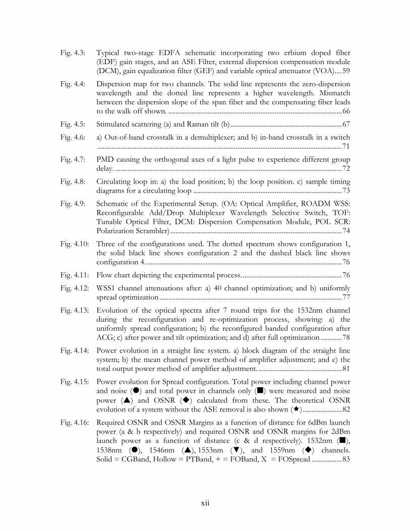
xii
Fig. 4.3: Typical two-stage EDFA schematic incorporating two erbium doped fiber (EDF) gain stages, and an ASE Filter, external dispersion compensation module (DCM), gain equalization filter (GEF) and variable optical attenuator (VOA)....59
Fig. 4.4: Dispersion map for two channels. The solid line represents the zero-dispersion wavelength and the dotted line represents a higher wavelength. Mismatch between the dispersion slope of the span fiber and the compensating fiber leads to the walk off shown. ..................................................................................................66
Fig. 4.5: Stimulated scattering (a) and Raman tilt (b)...............................................................67 Fig. 4.6: a) Out-of-band crosstalk in a demultiplexer; and b) in-band crosstalk in a switch
..........................................................................................................................................71 Fig. 4.7: PMD causing the orthogonal axes of a light pulse to experience different group
delay. ................................................................................................................................72 Fig. 4.8: Circulating loop in: a) the load position; b) the loop position. c) sample timing
diagrams for a circulating loop ....................................................................................73 Fig. 4.9: Schematic of the Experimental Setup. (OA: Optical Amplifier, ROADM WSS:
Reconfigurable Add/Drop Multiplexer Wavelength Selective Switch, TOF: Tunable Optical Filter, DCM: Dispersion Compensation Module, POL SCR: Polarization Scrambler).................................................................................................74
Fig. 4.10: Three of the configurations used. The dotted spectrum shows configuration 1, the solid black line shows configuration 2 and the dashed black line shows configuration 4. ..............................................................................................................76
Fig. 4.11: Flow chart depicting the experimental process. ........................................................76 Fig. 4.12: WSS1 channel attenuations after: a) 40 channel optimization; and b) uniformly
spread optimization .......................................................................................................77 Fig. 4.13: Evolution of the optical spectra after 7 round trips for the 1532nm channel
during the reconfiguration and re-optimization process, showing: a) the uniformly spread configuration; b) the reconfigured banded configuration after ACG; c) after power and tilt optimization; and d) after full optimization ............78
Fig. 4.14: Power evolution in a straight line system. a) block diagram of the straight line system; b) the mean channel power method of amplifier adjustment; and c) the total output power method of amplifier adjustment. ...............................................81
Fig. 4.15: Power evolution for Spread configuration. Total power including channel power and noise ( ) and total power in channels only ( ) were measured and noise power ( ) and OSNR ( ) calculated from these. The theoretical OSNR evolution of a system without the ASE removal is also shown ( )......................82
Fig. 4.16: Required OSNR and OSNR Margins as a function of distance for 6dBm launch power (a & b respectively) and required OSNR and OSNR margins for 2dBm launch power as a function of distance (c & d respectively). 1532nm ( ), 1538nm ( ), 1546nm ( ), 1553nm (▼), and 1559nm ( ) channels. Solid = CGBand, Hollow = PTBand, + = FOBand, X = FOSpread .................83
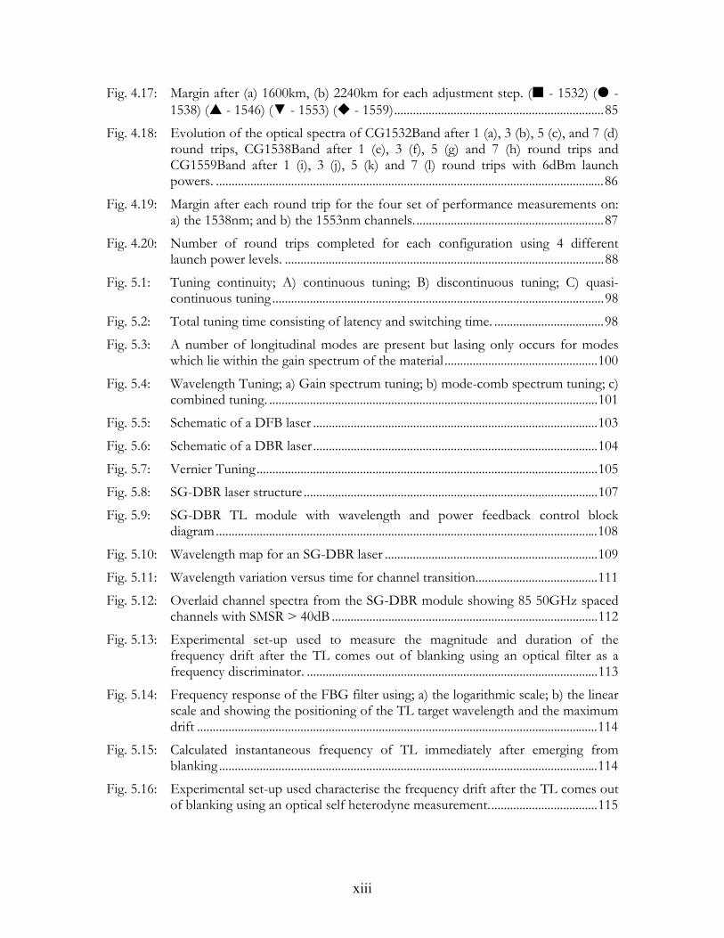
xiii
Fig. 4.17: Margin after (a) 1600km, (b) 2240km for each adjustment step. ( - 1532) ( - 1538) ( - 1546) (▼ - 1553) ( - 1559)...................................................................85
Fig. 4.18: Evolution of the optical spectra of CG1532Band after 1 (a), 3 (b), 5 (c), and 7 (d) round trips, CG1538Band after 1 (e), 3 (f), 5 (g) and 7 (h) round trips and CG1559Band after 1 (i), 3 (j), 5 (k) and 7 (l) round trips with 6dBm launch powers. ............................................................................................................................86
Fig. 4.19: Margin after each round trip for the four set of performance measurements on: a) the 1538nm; and b) the 1553nm channels.............................................................87
Fig. 4.20: Number of round trips completed for each configuration using 4 different launch power levels. ......................................................................................................88
Fig. 5.1: Tuning continuity; A) continuous tuning; B) discontinuous tuning; C) quasi-continuous tuning ..........................................................................................................98
Fig. 5.2: Total tuning time consisting of latency and switching time. ...................................98 Fig. 5.3: A number of longitudinal modes are present but lasing only occurs for modes
which lie within the gain spectrum of the material .................................................100 Fig. 5.4: Wavelength Tuning; a) Gain spectrum tuning; b) mode-comb spectrum tuning; c)
combined tuning. .........................................................................................................101 Fig. 5.5: Schematic of a DFB laser ...........................................................................................103 Fig. 5.6: Schematic of a DBR laser...........................................................................................104 Fig. 5.7: Vernier Tuning.............................................................................................................105 Fig. 5.8: SG-DBR laser structure ..............................................................................................107 Fig. 5.9: SG-DBR TL module with wavelength and power feedback control block
diagram..........................................................................................................................108 Fig. 5.10: Wavelength map for an SG-DBR laser ....................................................................109 Fig. 5.11: Wavelength variation versus time for channel transition.......................................111 Fig. 5.12: Overlaid channel spectra from the SG-DBR module showing 85 50GHz spaced
channels with SMSR > 40dB .....................................................................................112 Fig. 5.13: Experimental set-up used to measure the magnitude and duration of the
frequency drift after the TL comes out of blanking using an optical filter as a frequency discriminator. .............................................................................................113
Fig. 5.14: Frequency response of the FBG filter using; a) the logarithmic scale; b) the linear scale and showing the positioning of the TL target wavelength and the maximum drift ................................................................................................................................114
Fig. 5.15: Calculated instantaneous frequency of TL immediately after emerging from blanking .........................................................................................................................114
Fig. 5.16: Experimental set-up used characterise the frequency drift after the TL comes out of blanking using an optical self heterodyne measurement...................................115
xiv
Fig. 5.17: Frequency drift characterisation of TL module for channel transition 42-52 using frequency discriminator (top) with self heterodyne technique for comparison (bottom) ........................................................................................................................116
Fig. 5.18: General schematic of the tunable SFP laser ............................................................117 Fig. 5.19: Actual dimensions of tunable SFP ‘Device 1’ .........................................................118 Fig. 5.20: Photographs of mounted laser chips ........................................................................119 Fig. 5.21: Peak output wavelength as a function of current to the front and back section of
an SFP laser. .................................................................................................................120 Fig. 5.22: SMSR as a function of current to the front and back section of an SFP laser. ..120 Fig. 5.23: Overlaid single mode spectra of Device 1 showing SMSR >35dB for each
channel ..........................................................................................................................120 Fig. 5.24: Experimental configuration used to determine switching time of the laser.
Comprised of tunable laser (TL), tunable band pass filter (TF), photodetector (O/E).............................................................................................................................121
Fig. 5.25: Tunable laser switching between channels one and two with the filter set on channel one (top) and on channel two (bottom). ...................................................122
Fig. 5.26: Experimental setup for the heterodyne technique..................................................123 Fig. 5.27: Beating signal generated when output of switching laser is mixed with ECL signal
1 GHz away from 1 channel from slotted laser with (a) 10 ns/div (b) 500 ps/div.........................................................................................................................................123
Fig. 5.28: Experimental Setup used to measure the switching speed of a modulated SFP laser ................................................................................................................................124
Fig. 5.29: Switching SFP eye diagrams; a) Channel 1 exhibiting a switch on time of less than 500ps and channel 2 showing a switch off time of approximately 1ns; b) Channel 1 exhibiting a switch off time of less than 500ps and channel 2 showing a switch on time of less than 500ps. The dashed red line represents 4.5ns of the 10ns gating window which was stepped across to measure the time resolved BERs. Clearly for 1.5ns of this time 50% of the bits will be in error because the laser is on the other channel.......................................................................................125
Fig. 5.30: Plot showing the time resolved BERs for the switch on and switch off times of both channels. ..............................................................................................................126
Fig. 5.31: In a system with instantaneous switching and perfect data, movement of the gating window by 1 bit length can cause the error rate to change from a) error free; to b) 5x10⁻³ where one bit is in error 50% of the time..................................127
Fig. 5.32: Time resolved BER measurements showing how soon after the switching event, error free transmission is possible on (top) channel 1 and (bottom) channel 2.128
Fig. 6.1: Simulated 40Gb/s duobinary signal vs. 40Gb/s NRZ signal in the electrical domain (left) and experimental measurements in the optical domain (right) .....140
Fig. 6.2: SCM labelling scheme: a) Transmitter subsystem for SCM labelling scheme; b) resulting optical spectrum; Electrical inputs and outputs to diplexer including eye
xv
diagram of: c) duobinary payload; d) modulated 40GHz subcarrier; and e) and combined output..........................................................................................................141
Fig. 6.3: Receiver subsystem showing extracted spectra .......................................................143 Fig. 6.4: Optical spectra for: a) transmitted subcarrier-multiplexed signal; b) filtered
payload; c) filtered single side-band label .................................................................144 Fig. 6.5: Received Eye diagrams of: a) payload with label off; b) label with payload off; c)
payload with label on; and d) label with payload on...............................................144 Fig. 6.6: BER versus received power for: a) payload PRBS 27-1 with and without various
labels; b) labels of PRBS 27-1 with and without various payloads, where Pm = payload with PRBS 2m-1, Ln = label with PRBS 2n-1 .............................................145
Fig. 6.7: Total received power at BER 10-9 vs. reduction in gain of duobinary amplifier with and without labels/payloads; b) Label received power at BER 10-9 as a function of PRBS length of label with and without payload. (Pn = payload with PRBS 2n-1) ....................................................................................................................146
Fig. 6.8: Transmitter and receivers for subcarrier-multiplexed payload and label; TLS: tunable laser source, VOA: variable optical attenuator, PM: power meter, PD: photodiode, ED: error detector.................................................................................147
Fig. 6.9: Plot of measured BER versus received power for: a) payload PRBS 27-1 with and without label at different subcarrier phases; b) label of PRBS 27-1 with and without payload at maximum or minimum subcarrier phases ..............................147
Fig. 6.10: a) Measured receiver sensitivities of the payload and label versus subcarrier phase angle; b) Oscilloscope traces of electrical duobinary drive signal data pattern without subcarrier (i) and with subcarrier at Φmax (ii) and Φmin (iii), respectively....................................................................................................................148
Fig. 6.11: Experimental setup employing two fast tunable lasers (FTLs).............................149 Fig. 6.12: Spectra at different stages of the system: a) Two channels 100GHz apart; b)
suppressed labels at one port of AMZD; c) suppressed payload at second port of AMZD; d) extracted Label .........................................................................................150
Fig. 6.13: (a) Bit error rate of the 194 THz channel payload versus received power in one channel for 4 cases: single channel without label ( ); single labelled channel ( ); two static labelled channels ( ); two switching labelled channels ( ). (b) Bit error rate of the 194 THz channel label versus received power in one channel for 4 cases: single label without payload ( ); single channel label with payload ( ); two static channels ( ); two switching channels ( )............................................152
Fig. 6.14: Received eye diagrams of the payload (a) and label (b) for 2 static channel case........................................................................................................................................152
Fig. 6.15: Time Resolved Bit error rate measurements for the extracted label ( ) and instantaneous frequency of the switching laser’s label. The received power was approximately -28.5 dBm (a) laser at freq 192.1 THz, (b) laser blanked for 60ns, (c) laser settling into freq 193.94 THz for 200ns, (d) laser blanked for 60ns, (e)

xvi
laser at freq 192.1 THz for 200ns, (f) laser blanked for 60ns, (g) laser settling into freq 193.94 THz for 200ns.........................................................................................153

xvii
List of Acronyms ACA Amplifier Coupler Absorber ACG Applied Constant Gain ADM Add Drop Multiplexer AM Amplitude Modulation AM-PSK Amplitude Modulation-Phase Shift Keyed AMZD Asymmetric Mach-Zehnder Disinterleaver AO Acousto-Optic APD Avalanche Photodiode AR Anti Reflection ASE Applications Spontaneous Emission ASON Automatically Switched Optical Network ATM Asynchronous Transfer Mode AWG Arrayed Waveguide Gratings AWGR Arrayed Waveguide Grating Router BER Bit Error Rate BERT Bit Error Rate Tester CG Constant Gain CW Continuous Wave CWDM Coarse WDM DB Data Burst DBR Distributed Bragg Reflector DC Direct Current DCF Dispersion Compensation Fiber DCM Dispersion Compensation Module DCS Digital Cross Connect Switch DFA Doped Fiber Amplifiers DFB Distributed Feedback DGD Differential Group Delay DPSK Differential Phase Shift Keyed DSB Double Side Band DSF Dispersion Shifted Fiber DWDM Dense WDM EAM Electro Absorption Modulator ECL External Cavity Lasers ED Error Detector EDF Erbium Doped Fiber EDFA Erbium Doped Fiber Amplifiers EML Electro-Absorption Modulator Laser EO Electro Optic EPS Electronic Packet Switching ETDM Electrical Time Division Multiplexed FBG Fiber Bragg Grating FDL Fiber Delay Lines FDM Frequency Division Multiplexing

xviii
FEC Forward Error Correction FLM Fiber Loop Mirror FO Fully Optimized FP Fabry-Pérot FPGA Field Programmable Gate Array FSC Fiber Switch Capable FSR Free Spectral Range FTL Fast Tunable Lasers FWM Four Wave Mixing FXC Fiber Cross Connect GCSR Grating Coupled Sampled Reflector GEF Gain Equalization Filter GHz Gigahertz GMPLS Generalized Multi Protocol Label Switching IETF Internet Engineering Task Force IMD Intermodulation Distortion IP Internet Protocol ISDN Integrated Services Digital Network ISI Inter Symbol Interference ITU International Telecommunication Union ITU-T ITU Telecommunications Sector JET Just Enough Time JIT Just in Time L2SC Layer 2 Switch Capable LASER Light Amplification by Stimulated Emission of Radiation LD Laser Diode LO Local Oscillator LSC Lambda Switch Capable MEM Micro Electro Mechanical MEMS Micro Electro Mechanical Systems MGY Modulated Grating Y MHz Megahertz MPLS Multi Protocol Label Switching MZ Mach-Zehnder MZI Mach-Zehnder Interferometer MZM Mach Zehnder Modulator NF Noise Figure NNI Network to Network Interface NRZ Non Return to Zero NRZ-OOK Non Return to Zero On/OFF Keyed NZDSF Non Zero Dispersion Shifted Fiber OA Optical Amplifier OADM Optical Add Drop Multiplexers OBS Optical Burst Switching OCDM Optical Code Division Multiplexed OCS Optical Circuit Switching
xix
OCSS Optical Carrier Suppression and Separation OE Opto-electronic OEO Optical to Electrical to Optical OFS Optical Flow Switching OH Hydroxil OIF Optical Internetworking Forum OIS Optical IP Switching OLS Optical Label Switching OLT Optical Line Terminals OM Opto-Mechanical OPS Optical Packet Switching OSA Optical Spectrum Analyser OSNR Optical Signal to Noise Ratio OTDM Optical Time Division Multiplexing OTN Optical Transport Networks OXC Optical Cross Connect P-I Power vs. Current PD Photodiode PDG Polarization Dependent Gain PDL Polarization Dependent Loss PIN Positive Intrinsic Negative PM Power Meter PMD Polarization Mode Dispersion POL SCR Polarization Scrambler PPG Pulse Pattern Generator PRBS Pseudo Random Bit Sequence PSC Packet Switch Capable PSK Phase Shift Keyed PSTN Public Switched Telephone Network PT Power and Tilt PXC Photonic Cross Connect RAM Random Access Memory RF Radio Frequency ROADM Reconfigurable Optical Add Drop Multiplexers RZ Return to Zero SBS Stimulated Brillouin Scattering SCM Subcarrier Multiplexed SDH Synchronous Digital Hierarchy SDM Space Division Multiplexing SFP Slotted Fabry-Pérot SG Sampled Grating SG-DBR Sampled Grating Distributed Bragg Reflector SHB Spectral Hole Burning SLA Service Level Agreements SMA Sub miniature Version A SMSR Single Mode Spectra
xx
SOA Semiconductor Optical Amplifier SONET Synchronous Optical Network SPM Self Phase Modulation SRS Stimulated Raman Scattering SSB Single Sideband SSG Super Structure Grating SSMF Standard Single Mode Fiber STS-1 Synchronous Transport Signal TAG Tell and Go TAW Tell and Wait TDM Time Division Multiplex TF Tunable Filter THz Terahertz TL Tunable Laser TLS Tunable Laser Source TO Thermo-Optic TOF Tunable Optical Filter TTL Time to Live TWC Tunable Wavelength Converters UDWDM Ultra Dense WDM UNI User Network Interface UNI/NNI User Network Interface/Network Network Interface USA United States of America V-I Voltage - Current VCF Vertical Coupler Filter VCSEL Vertical Cavity Surface Emitting Lasers VMZ Vertical Mach Zehnder VOA Variable Optical Attenuator WBXC Waveband Cross Connect WDM Wavelength Division Multiplexed WIXC Wavelength Interchanging Cross Connect WSS Wavelength Selective Switch WSXC Wavelength Selective Cross Connect XC Cross Connect XGM Cross Gain Modulation XPM Cross Phase Modulation
1
Chapter 1 – Introduction
The widespread deployment of WDM technology has been driven by the massive growth in
the volume of data traffic since the dawn of the internet. Optical fiber, originally used to
carry a single wavelength channel now often carries 128 wavelengths or more. While the
technology for optical transport flourished, the technology for optical switching lagged
behind and this has led to a rigid, opaque network, in which OEO conversion is still
performed at the nodes and reconfiguration of the network can take weeks. The ongoing
deployment of optical switching components such as optical cross connects (OXCs) and
reconfigurable optical add/drop multiplexers (ROADMs) brings greater transparency and
reconfigurability to WDM networks and improves their efficiency, scalability and flexibility.
The immediate advantage brought by the deployment of these components is centralized
network management. Rather than having to deploy personnel to each node location, the
network can be reconfigured from a central office.
The next step for optical networks will see a move away from human management of the
network, to a network which will automatically self-reconfigure in response to changing
traffic demands, network faults or user requests. The control and monitoring systems
required for automatic operation represent a significant challenge and one aspect of this is
examined closely in this thesis. As the channel configuration changes, gain dynamics of the
amplifiers and the previous system arrangement can lead to channel power divergence that
can result in OSNR and nonlinearity related transmission penalties. The re-optimization of
the network for the new configuration can take seconds or longer and during this time
transmission may not be possible leading to a significant reduction in network throughput.
While OCS represents a leap forward for optical networking, there are also potential
drawbacks associated with its use for the backbone of the future Internet. Early arguments
against OCS related to the poor bandwidth efficiency and reduced robustness in comparison
to packet switching, however these arguments have largely been nullified [1]. More recent
arguments include issues with signalling complexity, the inherent blocking probability of
circuits and the fact that the current internet is designed for packets rather than circuits. As
such great interest has been seen in the development of optical packet switched systems and
2
yet the challenges for the development of OPS may be even greater than those facing OCS.
The lack of practical optical buffers and optical logic represent two of the major obstacles.
Wavelength tunable lasers (TLs) are becoming a mainstream component in today’s optical
networks due to the cost saving they offer, in terms of back-up transmitters and inventory
reduction. However in these roles the dexterity of TLs is not fully exploited; they really come
into their own as a key component in the transmitters and wavelength converters of OPS
networks that require switching between hundreds of wavelengths on nanosecond
timescales. As such, the accuracy of wavelength switching must be very precise. In this work
the switching times, wavelength accuracy and drift are all examined and the impact of these
properties on an OPS system is evaluated.
The work described in this thesis was supported by Science Foundation Ireland and was
carried out in the Radio and Optical Communications Laboratory, Dublin City University, in
the Photonic Systems Laboratory at the Tyndall National Institute, Cork and in Bell
Laboratories, Crawford Hill, New Jersey USA. It contributes to the body of knowledge in
three distinct areas:
Reconfiguration related performance penalties in OCS networks - This section of the work deals with
slow reconfigurable networks and the performance issues which can be encountered after
reconfiguration of the channels. To date, the effects of reconfiguration on transmission
performance has not been widely studied and the aim of this work was to stimulate further
experimentation in this area. Loading dependent gain variation in the EDFAs and the
historical system arrangement can lead to severe channel power divergence and hence,
transmission penalties due to OSNR degradation or non-linear effects. A technique was
developed that allows the detailed study of the post reconfiguration and post re-optimization
system performance in circulating loops. The experimental work was carried out on a WDM
circulating loop testbed in Bell Laboratories and is described in Chapter 3.
Switching and modulation of a slotted Fabry-Pérot laser - The second set of experiments is based on
the switching and modulation of a novel tunable laser developed by the III-V Devices and
Materials Group at the Tyndall National Institute. Tunable lasers are a key component for
future fast wavelength switching networks, however due to the complex fabrication
processes; tunable lasers that can tune very quickly over a wide wavelength range are very
costly. The fabrication process for the devices studied, which are known as tunable Slotted
3
Fabry-Pérot (SFP) lasers, is much simpler and it is expected that these devices could
potentially be used as in cost effective transmitters for access networks, for example. It was
shown for the first time in this work that these devices exhibit extremely fast wavelength
switching and can operate error free up to 10Gb/s. The tunable SFP devices were
characterised both in Dublin City University and in Bell Laboratories and the work carried
out is detailed in Chapter 4.
Wavelength drift in SCM optical label switched networks - The final set of experiments is based on a
commercially available Sampled Grating Distributed Bragg Reflector (SG-DBR) tunable laser
module by Intune Networks. These devices exhibit all of the properties required of a tunable
laser for use in an OPS network. To date, much of the literature in the area of OPS has
focussed on the transmission, address recognition and routing of various OPS schemes, and
the fact that these OPS schemes will be used in a multi-channel system with switching
tunable lasers has been somewhat neglected. In this work, a novel subcarrier multiplexed
(SCM) optical labelling scheme is developed and tested in a dual channel system employing
switching tunable lasers. Characterization of the wavelength drift of the laser was performed
and the impact of this drift in the optical packet switching system was examined. This work
was carried out in Dublin City University and in the Tyndall National Institute and it is
reported in Chapters 4 and 5.
The remainder of this thesis is structured into six chapters as follows:
Chapter One briefly discusses the history of optical communication and optical networking.
Wavelength division multiplexing is introduced along with the basic components of a WDM
optical network. Important issues relating to a number of the components are also
considered in this chapter for example the section on optical fiber discusses dispersion, non-
linearities, and attenuation. Where required these issues will be dealt with in greater detail in
later chapters.
Chapter Two is concerned with reconfigurable WDM optical networks. It begins by
presenting two of the trends observed in future optical networks, namely greater
reconfigurability, and greater transparency. The various optical switching technologies are
then discussed followed by a section describing the network elements that are currently
being deployed. The remainder of the chapter then reviews the current state of the art in
commercial networks, discussing optical circuit switching and the GMPLS control plane that
4
enables it, before turning to future optical switching techniques such as optical burst and
packet switching.
In Chapter Three the first set of experimental work is described. Prior to this however,
important background information that assists in the understanding of the experiment is
given. The design and operation of EDFAs and their gain dynamics are explained along with
performance degradation that can result from gain error induced power divergence. Also
discussed are circulating loops, employed in this work to achieve long haul distances with
limited resources. The remainder of the chapter goes on to describe the experimental
process and set-up, the results and the conclusions arrived at.
Chapter Four moves away from slow optical switching and deals with the tunable laser (TL),
a key enabler for fast optical switching. It begins by discussing the applications of TLs in
WDM networks and the properties they must exhibit to be suitable for these applications.
Some detail is given on the workings and mechanisms of TLs and some common designs are
described. Then two types of widely tunable laser, namely the sampled grating distributed
Bragg reflector (SG-DBR) and the tunable slotted Fabry-Pérot (SFP) are detailed along with
experimental work which was carried out to characterise them.
Chapter Five then takes some of the characterisation work performed in the previous
chapter and looks at how the issues raised affect an optical packet switching system. A
review of the literature in the area of optical label switching is provided before a description
of a novel optical labelling scheme developed within the confines of the project is given.
This labelling scheme is then characterised in both single and dual-channel systems and the
effects of wavelength drift of the TL is examined.
In Chapter Six the preceding work is summarized and the thesis conclusions are drawn.

5
References [1] P. Molinero-Fernandez., N. McKeown “TCP Switching: Exposing Circuits to IP”,
Standford Knowledgebase.
6
Chapter 2 – Optical Networks and Wavelength Division Multiplexing
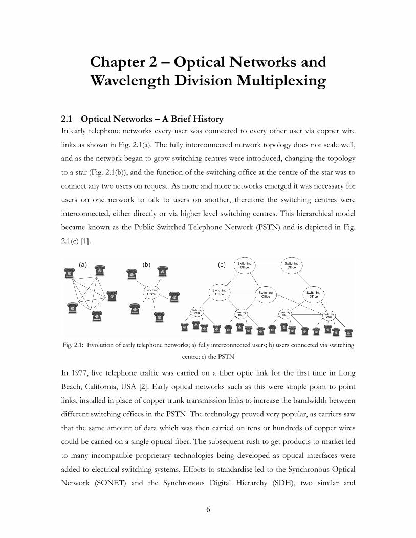
2.1 Optical Networks – A Brief History In early telephone networks every user was connected to every other user via copper wire
links as shown in Fig. 2.1(a). The fully interconnected network topology does not scale well,
and as the network began to grow switching centres were introduced, changing the topology
to a star (Fig. 2.1(b)), and the function of the switching office at the centre of the star was to
connect any two users on request. As more and more networks emerged it was necessary for
users on one network to talk to users on another, therefore the switching centres were
interconnected, either directly or via higher level switching centres. This hierarchical model
became known as the Public Switched Telephone Network (PSTN) and is depicted in Fig.
2.1(c) [1].
Fig. 2.1: Evolution of early telephone networks; a) fully interconnected users; b) users connected via switching
centre; c) the PSTN
In 1977, live telephone traffic was carried on a fiber optic link for the first time in Long
Beach, California, USA [2]. Early optical networks such as this were simple point to point
links, installed in place of copper trunk transmission links to increase the bandwidth between
different switching offices in the PSTN. The technology proved very popular, as carriers saw
that the same amount of data which was then carried on tens or hundreds of copper wires
could be carried on a single optical fiber. The subsequent rush to get products to market led
to many incompatible proprietary technologies being developed as optical interfaces were
added to electrical switching systems. Efforts to standardise led to the Synchronous Optical
Network (SONET) and the Synchronous Digital Hierarchy (SDH), two similar and
7
compatible standards which define the standard optical signals, a synchronous frame
structure and operating procedures [3,4]. SONET/SDH remains the dominant optical
telecommunication standards in use today.
The fundamental component of a SONET/SDH network is the Add/Drop Multiplexer
(ADM) that allows traffic to be taken off the network, and additional traffic to be coupled
onto the network at intermediate nodes. SONET/SDH networks are generally based on a
ring topology consisting of two optical fibers, one for each direction, or four fibers, one for
each direction and two for protection. While the bandwidth of SONET/SDH links is
scalable its upper bound was until quite recently limited to 10Gb/s by the electronics. As the
demand began to outgrow this available bandwidth, optical multiplexing techniques were
used to increase the capacity.
2.2 Optical Multiplexing Optical multiplexing techniques allow multiple data streams to be transmitted
simultaneously, thereby increasing total system capacity. The simplest method is Space
Division Multiplexing (SDM) in which the capacity of a system is increased by transmitting
additional data down a completely separate fiber. Unless the fiber plant is already place, this
multiplexing technique is expensive and avoided where possible. For this reason,
multiplexing techniques in which additional channels can be transmitted on a single fiber by
changing the terminating equipment have been developed. Such techniques include Optical
Time Division Multiplexing (OTDM) [5] in which short optical pulses are placed in a
particular time slot depending on which optical channel they belong to, Polarization Division
Multiplexing (PolDM) [6] in which channels are modulated onto orthogonal polarizations of
the same light such that they don’t interfere with each other, and Wavelength Division
Multiplexing (WDM) [7] in which data is modulated onto optical carriers at different
frequencies, which are then combined and transmitted down a single fiber. Each of the
techniques has advantages and disadvantages and indeed, they have been used
simultaneously in WDM/OTDM [8] for example.
At the time when bandwidth demand began to outgrow that available using time division
multiplexing in the electrical domain, WDM was the most mature of the optical multiplexing
techniques and it was adopted into many telecommunications carrier’s networks.
8
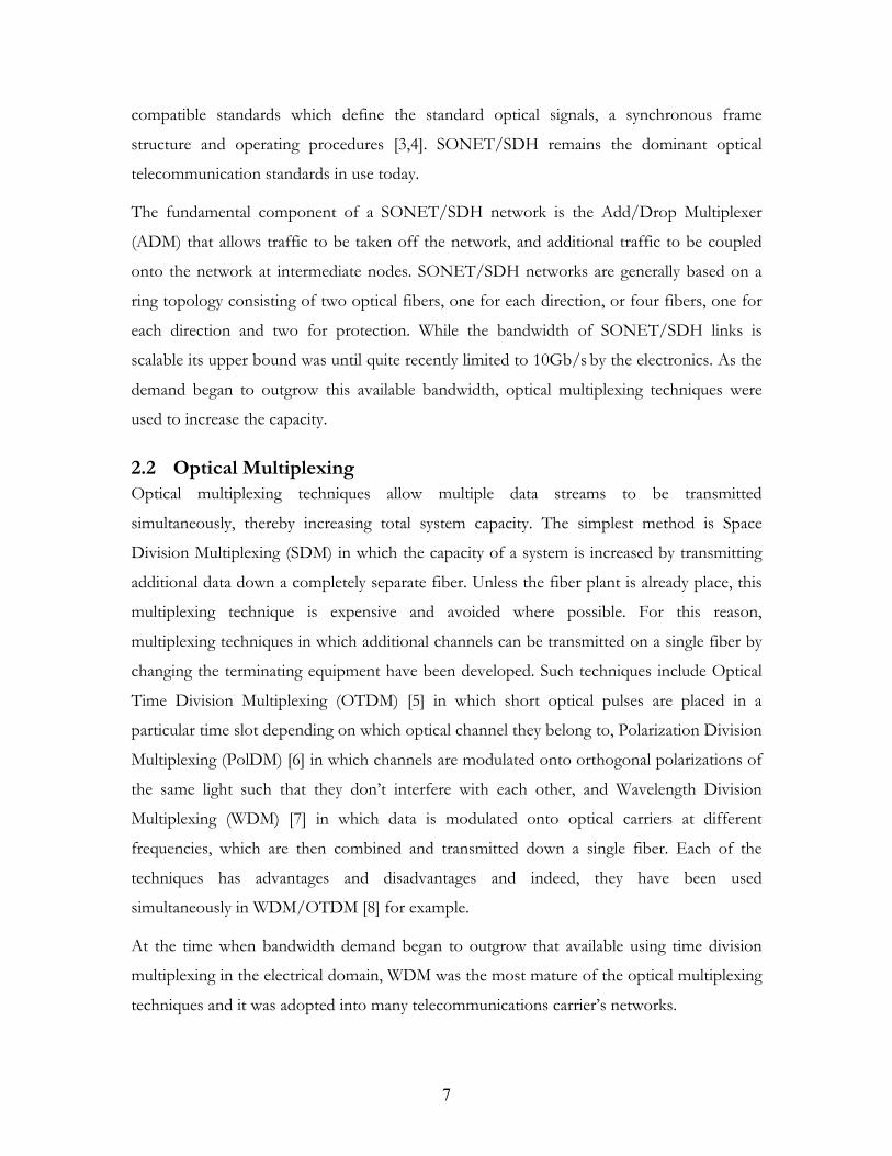
2.3 Wavelength Division Multiplexing WDM is analogous to Frequency Division Multiplexing (FDM) in Radio Frequency (RF) and
satellite communications but at much higher frequencies. The concept is illustrated in Fig.
2.2. Typically, electrical data channels with either Non-Return to Zero (NRZ) or Return to
Zero (RZ) line coding are modulated externally onto light at different wavelengths which are
generated by a number of Distributed Feedback (DFB) lasers. The different ‘colours’ of light
are combined using a multiplexer and transmitted over fiber to their destination. At their
destination a demultiplexer splits the combined light signal back into individual channels
which are then reverted to their original electrical form using photoreceivers.
In early WDM systems, regeneration of channels could only be carried out in the electrical
domain. Hence, at each regeneration point, the channels were demultiplexed and detected,
regenerated in the electrical domain and then re-modulated, re-multiplexed and re-
transmitted. This process formed an electronic bottleneck; it was slow and expensive both in
terms of the physical equipment required and in terms of power consumption.
Fig. 2.2: Point to point Wavelength Division Multiplexing; light from a number of sources are modulated with
different and multiplexed onto a single fiber for transmission. At the receiver the multi-wavelength signal is
demultiplexed into the individual channels which are each detected separately.
The development of the Erbium Doped Fiber Amplifier (EDFA) in 1987 and the
subsequent explosion in bandwidth demand due to the dawn of the Internet were the
catalysts which led to widespread WDM deployment. It was discovered that light with a
wavelength around 1550nm experienced strong gain when it was passed through silica fiber
doped with erbium atoms and pumped at 980nm or 1430nm [9, 10]. This allowed WDM
channels in this region to be amplified simultaneously without the need for demultiplexing
9
or Optical to Electrical to Optical (OEO) conversions. This important discovery prompted
the industry to change the wavelength band of choice for telecommunications from the
dispersion minimum at 1310nm to the EDFA gain peaks around 1550nm.
2.4 Classification of WDM Systems The two main categories of WDM in use today are Coarse WDM (CWDM) or Dense
WDM1 (DWDM). The classification depends on the frequency spacing between individual
channels. CWDM has channel spacing of 20nm spread evenly from 1270nm to 1610nm
yielding 18 usable channels [11]. Wide channel spacing such as this allows for the use of
inexpensive components and is suitable for systems with low bit rates, channel counts or
distances, such as access networks. DWDM uses much narrower channel spacing, ranging
from 3.2nm (400GHz) down to 0.4nm (50GHz) [12]. The DWDM channels are in the C and
L band of the electromagnetic spectrum corresponding to the EDFA amplification band. As
they require components of much higher specifications, they are generally only used in large
metro and long haul networks.
2.5 Major Optical Components of a DWDM network This section describes the major optical components used in current DWDM systems.
Today, switching is still performed electrically in most instances and therefore it will not be
discussed here. However, optical switching components will be covered in chapter 2.
2.5.1 Light Sources The light sources used in DWDM systems must exhibit high output power, high Side Mode
Suppression Ratio (SMSR), excellent wavelength stability, narrow line width and long
lifetime. Fabry-Pérot laser diodes are the simplest form of diode laser. In these devices a
semiconductor gain medium is sandwiched between two reflective surfaces to form a laser
cavity. They emit light in multiple modes making them unsuitable for WDM but the basic
structure can be adapted to form suitable WDM sources. Fabricated using Indium Gallium
Arsenide Phosphide (InGaAsP) waveguides, Distributed Feedback (DFB) lasers are similar
in structure to Fabry-Pérot laser but they include a frequency selective diffraction grating
[13] which sets the emission wavelength to the ITU grid recommendation G.694.1 [12]. DFB
lasers exhibit all of the desirable properties mentioned and are widely used in DWDM
1 The terms Wideband WDM (referring to multiplexing a channel at 1310nm and a channel at 1550nm) and Ultra Dense WDM (referring to channel spacing’s smaller than 50GHz for example 25GHz and 12.5GHz) are also sometimes used
10
networks. They generally incorporate temperature control to allow accurate fine tuning of
the emission wavelength and subsequent wavelength stability. The operation and structure of
laser diodes will be discussed in more detail in Chapter 5.
2.5.2 Modulators Data can be modulated onto four properties of light: the intensity, the frequency, the phase
and the polarisation. Intensity modulation is used almost exclusively in deployed networks,
although advanced modulation formats are receiving considerable interest lately. Intensity
modulation can be achieved via direct modulation of the drive current to the laser or
through the use of an external modulator. Direct modulation is not suitable for DWDM
because it causes an undesirable variation in the frequency of the emitted light known as
chirp, and in addition, data rates are limited by the bandwidth of the laser.
Two main types of external modulator are employed in today’s networks: The
Mach-Zehnder modulator (MZM) is based on the Electro-Optic (EO) (or Pockels) effect by
which the refractive index of a material changes with the application of an electric field, and
the Electro-Absorption Modulator (EAM), which is based on the Electro-Absorption (EA)
(or Franz-Keldysh) effect by which the absorption properties of a semiconductor are varied
by applying an electric field. MZMs exhibit much higher extinction ratio than EAMs (~25dB
vs. ~10dB) but in general they also need higher drive voltages [14]. In addition, while MZMs
are fabricated on Lithium Nibate, EAMs are fabricated using the same materials as lasers and
the two can be integrated on one chip to form an Electro-absorption Modulator Laser
(EML) [15]. These devices are attractive due to their small size and low drive voltage,
however while their chirp is small in comparison to direct modulation, it is non-zero and this
limits the achievable transmission distance.
2.5.3 Multiplexers/Demultiplexers Multiplexers are used to combine the various channels in the DWDM system into a single
fiber for transmission. Demultiplexers conversely, are used to separate the channels either
for switching at intermediate nodes or for detection at their destination. Multiplexers can be
built from simple passive power combiners that couple light from two separate fibers into a
single fiber although in practice, more sophisticated devices such as Arrayed Waveguide
Gratings (AWGs) are generally used. The task of demultiplexing is more complicated
because it requires specific wavelength selection, with good rejection of all other channels
11
and good stability over time. Most demultiplexers can also be used in reverse as multiplexers.
Devices for multiplexing can be either passive or active, and are based on either diffraction
or interference of the light signals.
Diffraction based demultiplexers make use of the Bragg effect. A Bragg grating or diffraction
grating in the optical path disperses the light spatially into wavelength components which
can then be focused into individual fibers using an array of grin lenses for example [16]. The
interference based demultiplexers include the AWG, the Mach-Zehnder (MZ) demultiplexer
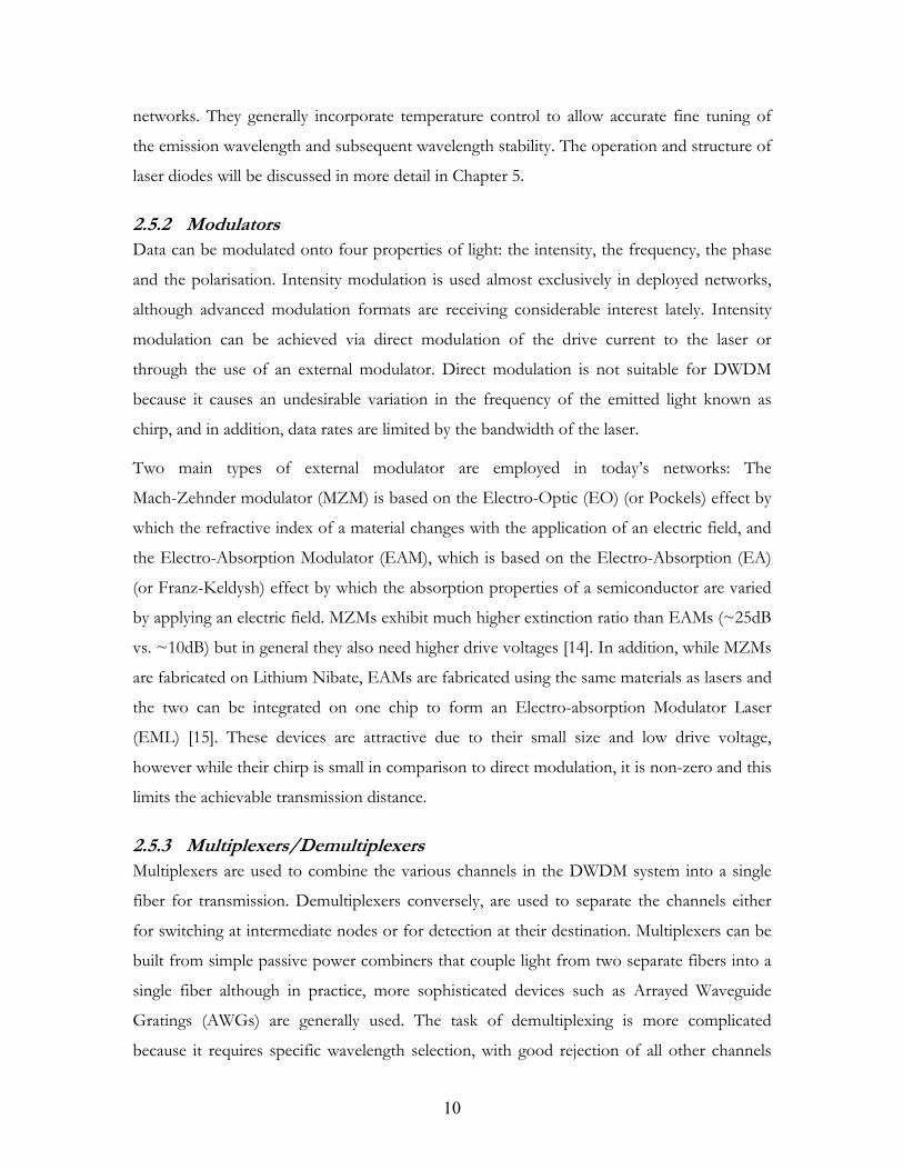
and étalon filter based demultiplexers. The basic operation of an AWG is shown in Fig. 2.3.
Light enters a free space star coupler which is followed by a number of waveguides of
slightly different lengths which introduce a different phase shift for each path. The output
light from each waveguide interferes constructively with the interference maximum at a
spatial position dependent on the phase shift. Thus each individual wavelength can be
focused onto an output fiber [17].
Fig. 2.3: An arrayed waveguide grating demultiplexer
MZ filters are created by splitting a light signal into two paths of different lengths and then
recombining them in an interference recombiner. The two signals will interfere with each
other constructively at periodic peak points and destructively elsewhere resulting in a
periodic passband. The MZ demultiplexer is based on a cascade of MZ filters which each
separate the spectrum into consecutively narrower portions. Because the insertion loss of
each stage is additive, these devices are unsuitable for large channel counts.
Fabry-Pérot Etalon Filters [18] are resonant cavities consisting of two reflective surfaces
designed such that while light at any wavelength can enter the cavity, only light which meets
12
the resonant conditions will be transmitted. Like the MZ filters, these are periodic filters
which must be cascaded to form a demultiplexer.
2.5.4 Fiber Most current DWDM systems use Standard Single Mode Fiber (SSMF) as their transmission
medium. Fiber requirements in terms of attenuation, dispersion, nonlinear performance are
stringent for long haul, high data rate networks.
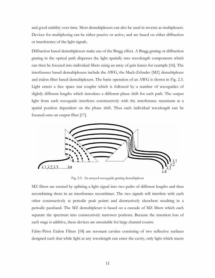
Attenuation Attenuation in optical fiber is primarily caused by absorption of the light by impurities in the
glass (primarily hydroxide (OH) ions), and by Rayleigh scattering of the light caused by
interactions between the photons and silica molecules. It is spectrally dependent and is at its
lowest around 1550nm as shown in Fig. 2.4. Optical fibers with increased purity have been
developed, [19] resulting in a significant reduction or elimination of the attenuation window
at 1400nm and leaving massive bandwidth available for exploitation.
Fig. 2.4: Attenuation and Dispersion in optical fiber as a function of wavelength
13
Dispersion Dispersion in SSMF causes light pulses to narrow or broaden as they travel through fiber.
An optical channel actually consists of a narrow band of wavelengths as opposed to a single
wavelength and because the refractive index of fiber is a function of wavelength, different
wavelengths traverse a fiber at different speeds. The natural dispersion minimum of SSMF is
at 1310nm but optical fibers have been designed with the dispersion zero shifted to other
wavelengths [20] as shown in Fig. 2.4. In addition, dispersion compensation fiber (DCF)
which has strong negative dispersion can be used to undo the negative effects of dispersion.
A certain amount of dispersion is acceptable or even desirable in a DWDM system as it
helps to reduce non-linear effects. However too much dispersion leads to data bits spreading
as they propagate through the fiber leading to Inter-Symbol Interference (ISI) which causes
bit errors at the receiver. The topic of dispersion will be re-visited in Chapter 4.
Non-linearities Optical fiber nonlinearities cause optical pulses to alter each other or themselves, and have
the effect of reducing the Optical Signal to Noise Ratio (OSNR) at the receiver. Two main
categories exist: those which result from refractive index variations in fiber when it is
exposed to different intensities of light such as Self Phase Modulation (SPM), Cross Phase
Modulation (XPM) and Four Wave Mixing (FWM), and those which result from stimulated
scattering such as Stimulated Raman Scattering (SRS) and Stimulated Brillouin Scattering
(SBS) [21]. These nonlinear effects will be discussed in greater detail in Chapter 4.
2.5.5 Amplifiers In a long haul link amplification is required to overcome losses in the system. There are three
types of optical amplifiers in use in DWDM systems. Doped Fiber Amplifiers (DFAs) and
especially the EDFA [9] are the most popular optical amplifier technology. Their fibers are
heavily doped with rare-earth elements such as erbium, and ytterbium which are excited to a
higher energy level by a pump laser. The excited ions emit a photon when they return to
their regular energy level by one of two processes. A signal photon with the correct
wavelength can disturb the excited atoms and in this case the recombination process will
cause the stimulated emission of a coherent photon, thereby causing amplification of the
signal. Alternatively, if the ion has not been disturbed it will recombine spontaneously after
it’s radiative lifetime and emit a photon with random wavelength and direction. Some of
14
these spontaneous photons will in turn be amplified causing amplified spontaneous emission
(ASE) which competes with the stimulated emission reducing the efficiency of amplification
and worsening the OSNR. Each rare earth element has a different emission wavelength, and
Erbium’s emission range is between 1530nm and 1565nm, which lies inside the absorption
minimum of fiber, making it very suitable for communications. EDFAs can be designed with
gain of up to 30dB, output power up to 30dBm and amplification windows of up to 50nm.
A DFA’s gain is not constant over its entire emission spectral range. For this reason, gain
flattening filters with a transfer function that is the inverse of the DFA’s gain function are
often used to flatten the spectrum [22,23]. In addition, the total gain is shared between all of
the amplified signals, and hence the addition, reduction or even reconfiguration of the
amplified channels leads to dynamic gain fluctuations. For long haul systems that may have
many amplified spans these gain fluctuations can contribute to serious performance
degradation. This issue will be closely examined in chapter 3.
Raman amplifiers [24] are the second common type of optical amplifiers used in
telecommunication. A high energy pump signal, a few tens of nanometres shorter in
wavelength that the signal to be amplified, is coupled into the transmission fibre. Due to
Stimulated Raman Scattering (SRS), a signal photon stimulates the scattering of a pump
photon in a process that creates a third photon identical to the incident signal photon.
Essentially the original signal photons ‘steals’ some of the energy from the pump signal
resulting in amplification of the original signal. Raman amplification generally occurs in the
transmission fiber forming a distributed amplifier with improved noise performance over
lumped amplifiers such as EDFAs. In addition, Raman amplifiers can provide gain at any
wavelength simply by using a number of pumps at different frequencies.
The third type of amplifier uses the optical gain mechanism in semiconductor materials and
is known as the Semiconductor Optical Amplifier (SOA) [25]. The structure of an SOA is
similar to that of a simple Fabry-Pérot laser cavity but with anti-reflective facets. As such, the
oscillation condition which causes lasing in a Fabry-Pérot laser does not exist. Electron-hole
pairs are created by electrically biasing the device and incident signal photons stimulate
recombination and the generation of a coherent photon, thereby causing gain.
SOAs can be integrated with lasers very easily and it is in this application, as transmitter
boosters for single channels, rather than for inline amplification of many DWDM channels,
15
that SOAs are generally used in WDM networks today. In general they are not used for
amplifying multiple channels because they suffer from Cross Gain Modulation (XGM),
which can cause serious crosstalk between channels. This process however, does allow
wavelength conversion using SOAs [26] and it seems likely that they will find a role in fast
switched WDM networks of the future.
2.5.6 Photoreceivers Two types of photodiode can be used to convert an optical signal back to the electrical
domain. The first is the Positive Intrinsic Negative (PIN) photodiode which consists of an
intrinsic layer sandwiched between a p-type layer and an n-type layer. When this structure is
reverse biased, and light is incident upon it, it generates a current which is proportional to
the intensity of the light. The ratio of the current generated to light absorbed is known as the
responsivity. For PINs this current is usually very small, so they are often coupled directly to
a transimpedence amplifier which converts the small current to a more useable voltage.
Receiver sensitivity can be greatly improved by using an avalanche photodiode (APD). The
device structure is similar to that of a PIN but with the ‘I’ layer designed to encourage
multiplication. A very large reverse bias is applied and this causes carriers to race across the
depletion layer with so much energy that they can create further carriers which in turn can
create further carriers and so on. The disadvantages of APDs are that they are noisier than
PINs and also the multiplication process reduces the response time and hence the
bandwidth of the device. Traditionally the bandwidth of APDs was limited to <5GHz but
advances in the technology have yielded APDs with bandwidths of 10GHz and higher
meaning that they could potentially be used in a DWDM system.
2.6 Conclusion and Perspective This chapter gave an introduction into WDM optical networks and discussed the technology
which enabled their widespread deployment. WDM eliminated the electrical bottleneck at
the transmitter side by allowing the transmission of multiple Electrical Time Division
Multiplexed (ETDM) signals on a fiber at the same time by placing them on WDM carriers,
and the EDFA eliminated the electrical bottleneck in the transmission path by removing the
need for OEO conversion of each channel at each regeneration point along the link. These
advancements have greatly increased the number of wavelength channels and data rate per
channel on the fiber links. At intermediate nodes however, switching is still performed in the
16
electrical domain requiring OEO conversions for every channel. This creates a bandwidth
mismatch between link capacity and switching capacity. Terminating each wavelength at each
node for routing is expensive, inflexible and scales poorly. Optical switching is seen as the
solution to this problem. Its introduction into networks will mean that signals can remain in
the optical domain throughout the network, and OE (or OEO) conversion will only be
required at the edge of the network in order to enter a separate access or client network.
Various forms of Optical Switching technologies and techniques will be discussed in detail in
Chapter 2.
17
References [1] T. S. El-Bawab, "Preliminaries and terminologies," in Optical Switching T. S. El-Bawab,
2006
[2] J. Hecht, City of Light: The Story of Fiber Optics. Oxford University Press, 1999
[3] ANSI T1.105: Digital Hierarchy Optical Rates and Formats Specification (SONET)
[4] CCITT (ITU) Recommendation G.707, "Synchronous Digital Hierarchy Bit Rates."
[5] R. S. Tucker, “Optical time-division multiplexing and demultiplexing in a
multigigabit/second fibre transmission system”, Electronics Letters 23(5), pp. 208-209, 1987.
[6] P.M.Hill, R. Olshansky, W.K Burns, "Optical polarization division multiplexing at 4
Gb/s," IEEE Photonics Technology Letters, vol.4, no.5, pp.500-502, May 1992
[7] S. Sugimoto, K. Minemura, K. Kobayashi et al, "High-speed digital-signal
transmission experiments by optical wavelength-division multiplexing," Electronics Letters ,
vol.13, no.22, pp.680-682, October 27 1977
[8] H. Tanaka, M. Hayashi, T. Otani, K. Ohara, M. Suz, "60 Gb/s WDM-OTDM
transmultiplexing using an electro-absorption modulator," Optical Fiber Communication
Conference and Exhibit, 2001. OFC 2001 , vol.1, no., pp. ME4-1-ME4-3 vol.1, 17-22 March
2001
[9] R. Mears, L. Reekie, I. Jauncey, and D. Payne, "High-gain rare-earth-doped fiber
amplifier at 1.54µm," in Optical Fiber Communication, 1987 OSA Technical Digest Series
(Optical Society of America, 1987), paper WI2.
[10] E. Desurvire, J. R. Simpson, and P. C. Becker, "High-gain erbium-doped traveling-
wave fiber amplifier," Opt. Lett. 12, 888- (1987)
[11] ITU Recommendation G.694.2, "Spectral Grids for WDM Applications: CWDM
Wavelength Grid"
[12] ITU Recommendation G.694.2, "Spectral Grids for WDM Applications: DWDM
Wavelength Grid"
18
[13] H. Kogelnik and C. V. Shank, “Stimulated Emission In A Periodic Structure” Appl.
Phys. Lett. 18, 152 (1971)
[14] S. V.Kartalopoulos, DWDM Networks Devices and Technology, Wiley-Interscience, New
Jersey, 2003
[15] H.Soda, M. Furutsu, K. Sato, N. Okazaki, S. Yamazaki, H. Nishimoto, H. Ishikawa,
"High-power and high-speed semi-insulating BH structure monolithic electroabsorption
modulator/DFB laser light source," Electronics Letters , vol.26, no.1, pp.9-10, 4 Jan 1990
[16] J. Lipson, W. Minford, E. Murphy, T. Rice, R. Linke, G. Harvey, "A six-channel
wavelength multiplexer and demultiplexer for single mode systems," Lightwave Technology,
Journal of , vol.3, no.5, pp. 1159-1163, Oct 1985
[17] C. Dragone, "An N*N optical multiplexer using a planar arrangement of two star
couplers," Photonics Technology Letters, IEEE , vol.3, no.9, pp.812-815, Sept. 1991
[18] J.Stone, L.W. Stulz, "Pigtailed high-finesse tunable fibre Fabry-Pérot interferometers
with large, medium and small free spectral ranges," Electronics Letters , vol.23, no.15, pp.781-
783, July 16 1987
[19] A. K. Srivastava et al, "High-speed WDM Transmission in AllWaveTM Fiber in
Both the 1.4-µm and 1.55-µm Bands," in Optical Amplifiers and Their Applications, D. Baney, K.
Emura, and J. Wiesenfeld, eds., Vol. 25 of OSA Trends in Optics and Photonics Series
(Optical Society of America, 1998), paper CA3
[20] L.G Cohen, C. Lin, W.G French, "Tailoring zero chromatic dispersion into the 1.5-
1.6 µm low-loss spectral region of single-mode fibres," Electronics Letters , vol.15, no.12,
pp.334-335, June 7 1979
[21] P. Bayvel, and R. Killey, , “Nonlinear Optical Effects in WDM transmission” in
Optical Fibre Telecommunications IV-A: Components, Academic Press, California, USA
2002
[22] M. Yamada, T. Kanamori, Y. Terunuma, K. Oikawa, M. Shimizu, S. Sudo, and K.
Sagawa, “Fluoride-based erbium-doped fiber amplifier with inherently flat gain response,”
IEEE Photon. Technol. Lett., vol. 8, no. 6, pp. 882–884, Jun. 1996.
19
[23] P. F. Wysocki, J. B. Judkins, R. P. Espindola, M. Andrejco, and A. M. Vengsarkar,
“Broad-band erbium-doped fiber amplifier flattened beyond 40 nm using long period grating
filter,” IEEE Photon. Technol. Lett., vol. 9, no. 10, pp. 1343–1345, Oct. 1997.
[24] E. Desurvire, M. Papuchan, J. P. Pocholle, J. Raffy, , and D. B. Ostrowsky, 'High
gain optical amplification of laser diode signal by Raman scattering in single mode fibres',
Electron. Lett., 1983,19, pp.751-753
[25] L. H. Spiekman, , “Semiconductor Optical Amplifiers” in Optical Fibre
Telecommunications IV-A: Components, Academic Press, California, USA 2002
[26] B.C. Gopal, F.S. Choa, , "Comparative study of wavelength conversion schemes
using semiconductor optical amplifiers," Lasers and Electro-Optics Society Annual Meeting, 1995.
8th Annual Meeting Conference Proceedings, Volume 1., IEEE , vol.2, no., pp.245-246 vol.2, 30
Oct-2 Nov 1995
20
Chapter 3 – Reconfiguration in WDM Networks and Optical Switching
3.1 Introduction As discussed in the previous chapter, the tremendous growth of the internet throughout the
1990s and up to the present has led to extensive deployment of Wavelength Division
Multiplexing (WDM). Initial WDM networks were point to point links between electronic
end terminals. The development of the Erbium Doped Fibre Amplifier (EDFA), as well as
improvements in each of the enabling technologies mentioned in Chapter 2 meant that large
numbers of wavelengths could be transmitted over thousands of kilometres. However,
because the technology for optical transport matured much earlier than the technology for
optical switching, which is still maturing, a high capacity optical transport network was built
on top of a legacy electronic switching system. This has led to a rigid network, in which
Optical-Electrical-Optical (OEO) conversion is still performed at the intermediate nodes
and changes to the network can take months, and to yet another electronic bottleneck – the
switching bottleneck. Two major trends which have emerged in optical networking are the
trend towards greater transparency and the trend towards higher levels of reconfigurability.
Improvement in these properties of the network will enable a more flexible, more scalable,
and more bandwidth efficient network suitable for the provision of next generation services.
This chapter will begin by discussing the trends of transparency and reconfigurability
mentioned. It will then give some insight into optical switching technologies before
discussing the main techniques of optical switching, namely Optical Circuit Switching (OCS),
Optical Burst Switching (OBS) and Optical Packet Switching (OPS) as well as two other
techniques, optical IP switching (OIS) and optical flow switching (OFS). OCS and OPS were
actively studied as part of this PhD, and so will receive greater attention than the other
methods.
3.2 Transparency A transparent optical system is one in which the data remains in the optical domain
throughout. Conversely, an opaque system requires the data to be converted back to
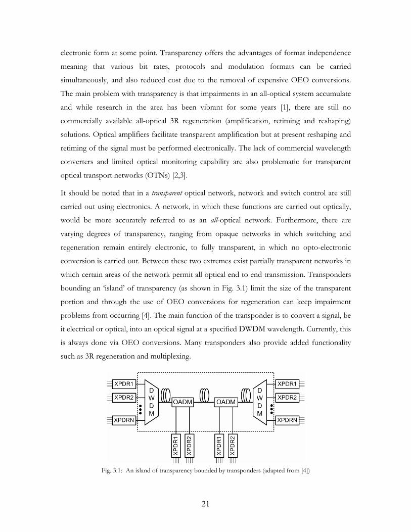
21
electronic form at some point. Transparency offers the advantages of format independence
meaning that various bit rates, protocols and modulation formats can be carried
simultaneously, and also reduced cost due to the removal of expensive OEO conversions.
The main problem with transparency is that impairments in an all-optical system accumulate
and while research in the area has been vibrant for some years [1], there are still no
commercially available all-optical 3R regeneration (amplification, retiming and reshaping)
solutions. Optical amplifiers facilitate transparent amplification but at present reshaping and
retiming of the signal must be performed electronically. The lack of commercial wavelength
converters and limited optical monitoring capability are also problematic for transparent
optical transport networks (OTNs) [2,3].
It should be noted that in a transparent optical network, network and switch control are still
carried out using electronics. A network, in which these functions are carried out optically,
would be more accurately referred to as an all-optical network. Furthermore, there are
varying degrees of transparency, ranging from opaque networks in which switching and
regeneration remain entirely electronic, to fully transparent, in which no opto-electronic
conversion is carried out. Between these two extremes exist partially transparent networks in
which certain areas of the network permit all optical end to end transmission. Transponders
bounding an ‘island’ of transparency (as shown in Fig. 3.1) limit the size of the transparent
portion and through the use of OEO conversions for regeneration can keep impairment
problems from occurring [4]. The main function of the transponder is to convert a signal, be
it electrical or optical, into an optical signal at a specified DWDM wavelength. Currently, this
is always done via OEO conversions. Many transponders also provide added functionality
such as 3R regeneration and multiplexing.
Fig. 3.1: An island of transparency bounded by transponders (adapted from [4])
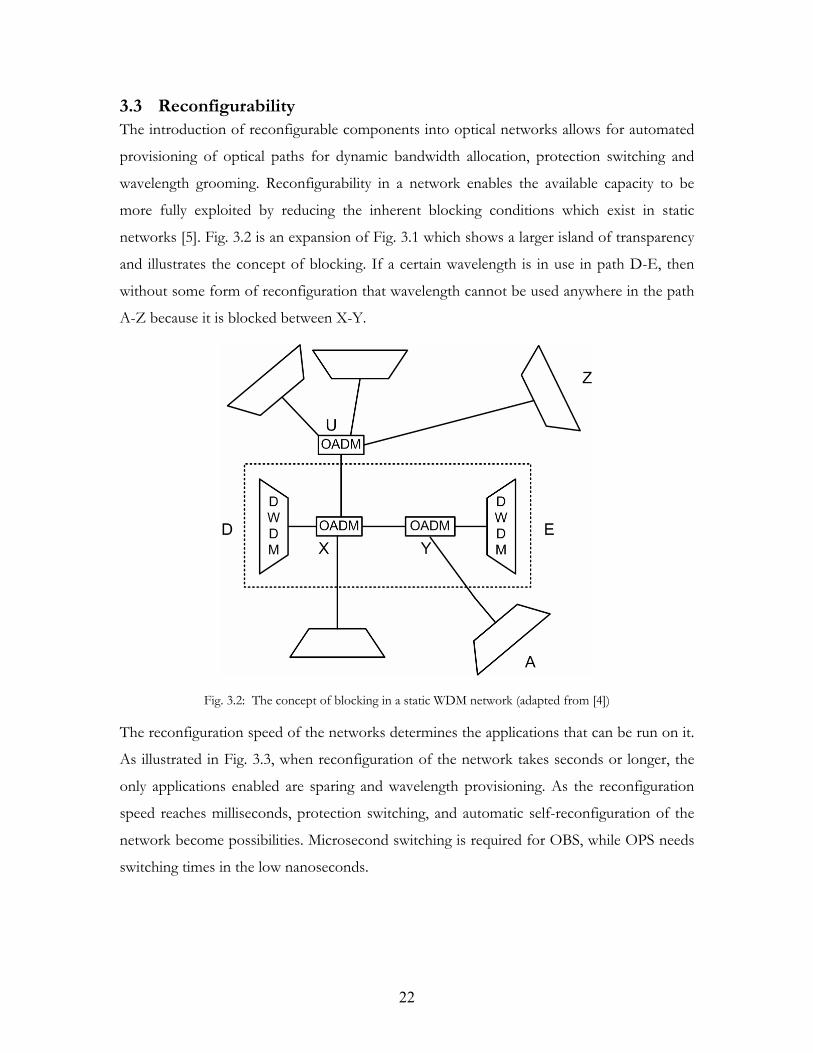
22
3.3 Reconfigurability The introduction of reconfigurable components into optical networks allows for automated
provisioning of optical paths for dynamic bandwidth allocation, protection switching and
wavelength grooming. Reconfigurability in a network enables the available capacity to be
more fully exploited by reducing the inherent blocking conditions which exist in static
networks [5]. Fig. 3.2 is an expansion of Fig. 3.1 which shows a larger island of transparency
and illustrates the concept of blocking. If a certain wavelength is in use in path D-E, then
without some form of reconfiguration that wavelength cannot be used anywhere in the path
A-Z because it is blocked between X-Y.
Fig. 3.2: The concept of blocking in a static WDM network (adapted from [4])
The reconfiguration speed of the networks determines the applications that can be run on it.
As illustrated in Fig. 3.3, when reconfiguration of the network takes seconds or longer, the
only applications enabled are sparing and wavelength provisioning. As the reconfiguration
speed reaches milliseconds, protection switching, and automatic self-reconfiguration of the
network become possibilities. Microsecond switching is required for OBS, while OPS needs
switching times in the low nanoseconds.
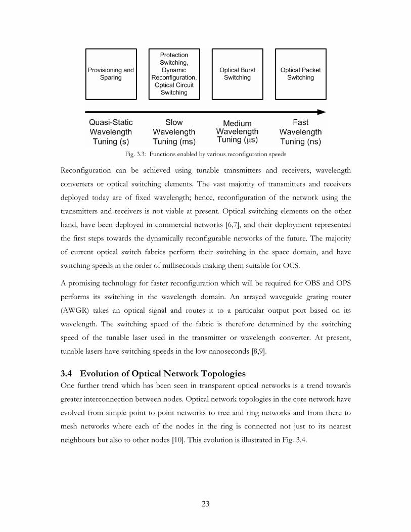
23
Fig. 3.3: Functions enabled by various reconfiguration speeds
Reconfiguration can be achieved using tunable transmitters and receivers, wavelength
converters or optical switching elements. The vast majority of transmitters and receivers
deployed today are of fixed wavelength; hence, reconfiguration of the network using the
transmitters and receivers is not viable at present. Optical switching elements on the other
hand, have been deployed in commercial networks [6,7], and their deployment represented
the first steps towards the dynamically reconfigurable networks of the future. The majority
of current optical switch fabrics perform their switching in the space domain, and have
switching speeds in the order of milliseconds making them suitable for OCS.
A promising technology for faster reconfiguration which will be required for OBS and OPS
performs its switching in the wavelength domain. An arrayed waveguide grating router
(AWGR) takes an optical signal and routes it to a particular output port based on its
wavelength. The switching speed of the fabric is therefore determined by the switching
speed of the tunable laser used in the transmitter or wavelength converter. At present,
tunable lasers have switching speeds in the low nanoseconds [8,9].
3.4 Evolution of Optical Network Topologies One further trend which has been seen in transparent optical networks is a trend towards
greater interconnection between nodes. Optical network topologies in the core network have
evolved from simple point to point networks to tree and ring networks and from there to
mesh networks where each of the nodes in the ring is connected not just to its nearest
neighbours but also to other nodes [10]. This evolution is illustrated in Fig. 3.4.
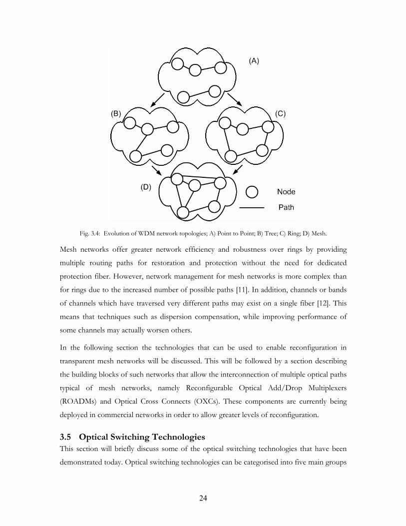
24
Fig. 3.4: Evolution of WDM network topologies; A) Point to Point; B) Tree; C) Ring; D) Mesh.
Mesh networks offer greater network efficiency and robustness over rings by providing
multiple routing paths for restoration and protection without the need for dedicated
protection fiber. However, network management for mesh networks is more complex than
for rings due to the increased number of possible paths [11]. In addition, channels or bands
of channels which have traversed very different paths may exist on a single fiber [12]. This
means that techniques such as dispersion compensation, while improving performance of
some channels may actually worsen others.
In the following section the technologies that can be used to enable reconfiguration in
transparent mesh networks will be discussed. This will be followed by a section describing
the building blocks of such networks that allow the interconnection of multiple optical paths
typical of mesh networks, namely Reconfigurable Optical Add/Drop Multiplexers
(ROADMs) and Optical Cross Connects (OXCs). These components are currently being
deployed in commercial networks in order to allow greater levels of reconfiguration.
3.5 Optical Switching Technologies This section will briefly discuss some of the optical switching technologies that have been
demonstrated today. Optical switching technologies can be categorised into five main groups
25
depending on the method used to induce the switching. Numbers 1-3 and 5 below are
generally based on guided wave switching (using optical fiber or waveguides) while switching
in number 4 usually occurs in free-space (with the exception of the bubble switch). Note that
here we only discuss the most common and promising technologies. More exhaustive lists
and comparisons of techniques can be found in [13-15]
1. Electro-Optic switching
The most common Electro-Optic (EO) switches are based on the Pockels (or electro-
optic) effect by which the refractive index of a material changes proportionally with an
applied electric field. This refractive index change can be used to direct light through a
waveguide. Lithium Nibate [16] (LiNbO3) is the most common material used because it
exhibits a large EO effect, and it is also readily fabricated into low loss planar waveguides
[17]. EO switching has also been demonstrated in liquid crystals and in SOAs used as
ON-OFF gates by varying the bias current [18]. Switching speeds ranging from
microseconds to nanoseconds have been demonstrated using different EO switching
technologies.
2. Acousto-Optic switching
Acousto-Optic (AO) switching has also been demonstrated with LiNbO3 but Tellurium
Dioxide (TeO2) is more commonly used. In an AO switch, ultra-sonic waves are used to
deflect light into different paths. On applying an RF electric field to the material, the
piezoelectric effect generates an acoustic wave that modulates the refractive index of the
material [19] enabling light to be directed through a waveguide. Typical switching speeds
are in the order of hundreds of nanoseconds.
3. Thermo-Optic switching
Mainly fabricated using silica and polymers, Thermo-Optic (TO) switches use the TO
effect by which the refractive index of the material is dependent on temperature. By
supplying current to heating elements alongside the waveguide, the refractive index can
be varied in order to direct the light in one direction or another. Switching speeds are
generally in the millisecond range.
26
4. Opto-Mechanical switching
This category consists of a number of techniques in which the switching comes about
through the movement of some component of the switch. Early OM switches involved
the movement of optical fibers to switch the light [20]. More modern technology
includes Micro-Electro-Mechanical Systems (MEMS) [14] that generally use matrices of
tiny mirrors to block, pass or redirect light, and bubble switches [21], in which an air
bubble at the crosspoint of a planar waveguide can be moved to redirect the light. The
free space OM switches can switch on millisecond timescales.
5. All-Optical switching
Switching has also been demonstrated using an optical signal for control. In SOAs ultra-
fast optical switching has been demonstrated using non-linear interferometry [22]
whereby an optical control signal is used to interfere with the data signal either
constructively or destructively in order to pass or block light. In addition, SOAs can be
used as wavelength converters [23] that allow switching or routing in the wavelength
domain using Arrayed Waveguide Grating Routers (AWGRs). Sub-nanosecond
switching speeds can be achieved with SOAs.
The scalability of optical switches built using the aforementioned technologies is a very
important issue. To be used in Cross-Connects (XCs) the switching technology must exhibit
low loss in order to be highly scalable to hundreds or thousands of ports. Typically the low
loss devices are the free space type based on beam steering and these exhibit slower
switching speeds. On the other hand the waveguide based switches offer the potential for
much faster switching with speeds matching or exceeding those required for OPS. The
losses in these switches accumulate more quickly however, which makes it difficult to
construct large port count XCs.
3.6 Elements of an Optical Switching Network The main building blocks of the optical layer are illustrated in Fig. 3.5 and are described
below. Note that in each case, transmission is only shown in a single direction. In reality,
these components would support transmission in both directions.
27
3.6.1 Optical Line Terminals Optical Line Terminals (OLTs), as shown in Fig. 3.5(a), are used to interface between fiber
transmission links and the switching elements such as ROADMs and XCs. A generic OLT
will contain a mux/demux to group a number of channels together and an amplifier to boost
the signal prior to transmission or reception, and may also contain transponders to adapt the
signal from client layers into a single WDM channel for transmission in the optical layer or
to perform OEO conversions if an electrical switch fabric is used. OLTs can be included as
part of a ROADM or XC, however due to poor standardization of WDM equipment; they
are generally treated as separate components which prevents interoperability problems
between equipment from different vendors.
3.6.2 ROADMs Optical Add Drop Multiplexers (OADMs) were added to WDM networks to allow access to
channels at intermediate points along a link that could be thousands of kilometres long.
Essentially an OADM consists of a demultiplexer followed by a multiplexer with some
filtration between the two. Channels or groups of channels can be dropped from and added
to the main path using an OADM and the wavelengths that remain on their current path are
known as the cut-through or express channels. One of the disadvantages of OADMs is that
they are essentially fixed devices. The channels which are to be added and dropped must be
chosen during the design phase and reconfiguring requires considerable Operational
Expenditure (OpEx) because a technician must visit every node in order to configure the
changes. The ROADM alleviates this problem by allowing remote reconfiguration of the
channels which are added and dropped at the intermediate node. Rather than having static
filtration elements between a mux/demux pair, ROADMs have a switching fabric as
illustrated in Fig. 3.5(b). This gives them the ability to add or drop any wavelength and can
enable, for example, dynamic provisioning of services in cases of unpredictable bandwidth
demand. This flexibility is very desirable to carriers and they have begun to deploy
ROADMs in their networks [7].
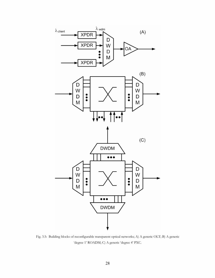
28
Fig. 3.5: Building blocks of reconfigurable transparent optical networks; A) A generic OLT; B) A generic
‘degree 1’ ROADM; C) A generic ‘degree 4’ PXC.
29
3.6.3 Cross Connects While, in general a ROADM is used to add data to or drop data from a single WDM path, at
a location where two or more WDM paths meet, there is a requirement for a XC. XCs
switch data from an incoming WDM path onto any one of a number of outgoing WDM
paths. In Fig. 3.5(c) the XC switches any channel from the West to either the North, South
or East path. Note that in a practical XC, signals could arrive from any of the 4 directions. If
this location also requires add/drop functionality (as is often the case) a multi-degree
ROADM with XC functionality must be used. These devices have the ability to add or drop
individual wavelengths from many paths or to switch them transparently onto any outgoing
path if they are not required at the particular node.
Many varieties of XC exist [24, 25]:
1. Digital Cross-connect Switches (DCSs) accept a WDM signal but then
demultiplex it in wavelength and time to a number of SONET STS-1 (50Mb/s)
streams. All functions including switching, performance monitoring and
regeneration are performed electrically. Such switches can be described as opto-
electronic switches but because they do not employ optical switching they will
not be discussed further here.
2. Optical Cross Connects (OXCs) are loosely and ambiguously defined and can be
found in the literature with either electrical or optical switching cores and with
varying levels of transparency. The advantages of these semi-transparent XCs
over their fully transparent counterparts (described next) are that because OEO
conversions are used, functions such as performance monitoring, wavelength
conversion and 3R regeneration are readily available. The disadvantage is that
these OEO conversions are expensive in terms of both equipment and power,
and in general they are performed whether required or not, which is
uneconomical.
3. Photonic Cross Connects (PXCs) are fully transparent XCs with an optical
switching fabric however control and processing remains electronic. The
advantages and disadvantages of total transparency are the converse of those
listed above. Unless optical wavelength conversion is employed PXCs are
blocking in the wavelength domain, which can complicate network management.
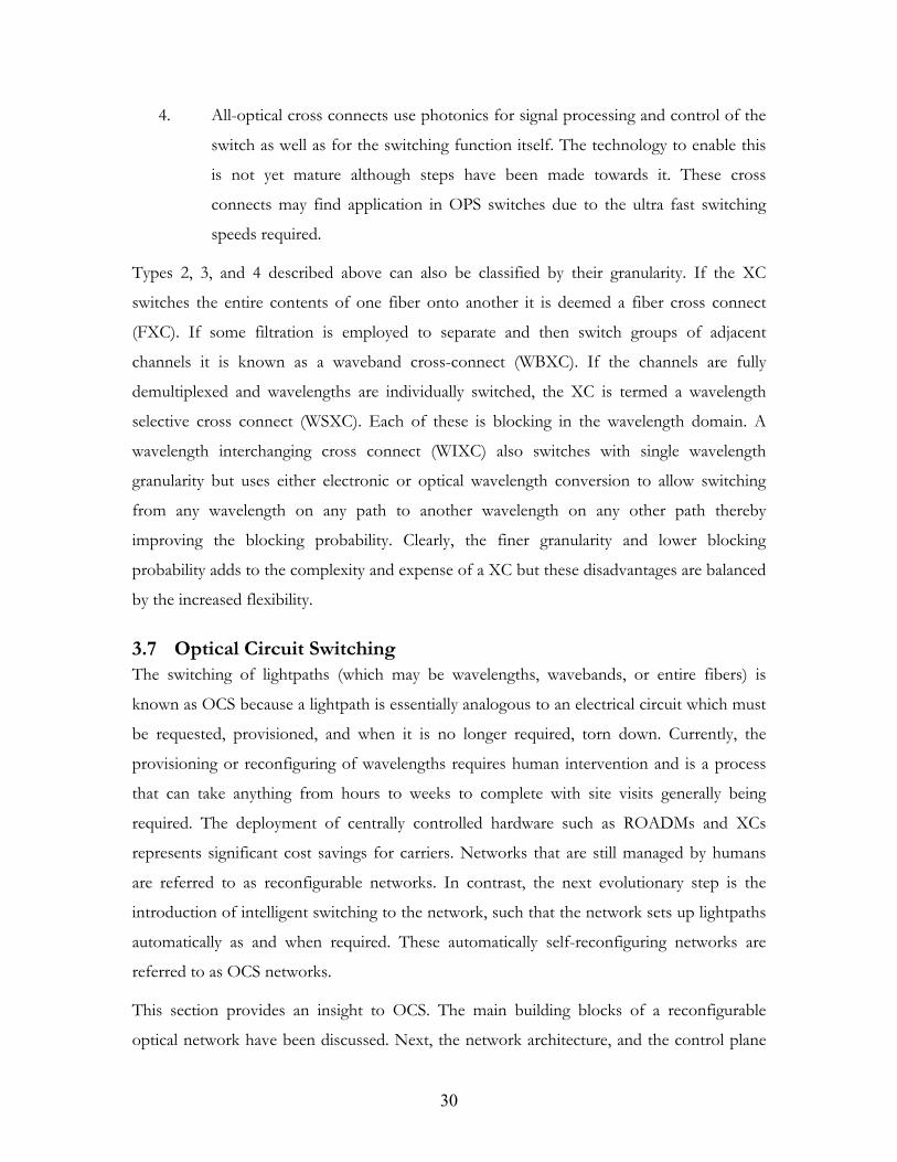
30
4. All-optical cross connects use photonics for signal processing and control of the
switch as well as for the switching function itself. The technology to enable this
is not yet mature although steps have been made towards it. These cross
connects may find application in OPS switches due to the ultra fast switching
speeds required.
Types 2, 3, and 4 described above can also be classified by their granularity. If the XC
switches the entire contents of one fiber onto another it is deemed a fiber cross connect
(FXC). If some filtration is employed to separate and then switch groups of adjacent
channels it is known as a waveband cross-connect (WBXC). If the channels are fully
demultiplexed and wavelengths are individually switched, the XC is termed a wavelength
selective cross connect (WSXC). Each of these is blocking in the wavelength domain. A
wavelength interchanging cross connect (WIXC) also switches with single wavelength
granularity but uses either electronic or optical wavelength conversion to allow switching
from any wavelength on any path to another wavelength on any other path thereby
improving the blocking probability. Clearly, the finer granularity and lower blocking
probability adds to the complexity and expense of a XC but these disadvantages are balanced
by the increased flexibility.
3.7 Optical Circuit Switching The switching of lightpaths (which may be wavelengths, wavebands, or entire fibers) is
known as OCS because a lightpath is essentially analogous to an electrical circuit which must
be requested, provisioned, and when it is no longer required, torn down. Currently, the
provisioning or reconfiguring of wavelengths requires human intervention and is a process
that can take anything from hours to weeks to complete with site visits generally being
required. The deployment of centrally controlled hardware such as ROADMs and XCs
represents significant cost savings for carriers. Networks that are still managed by humans
are referred to as reconfigurable networks. In contrast, the next evolutionary step is the
introduction of intelligent switching to the network, such that the network sets up lightpaths
automatically as and when required. These automatically self-reconfiguring networks are
referred to as OCS networks.
This section provides an insight to OCS. The main building blocks of a reconfigurable
optical network have been discussed. Next, the network architecture, and the control plane
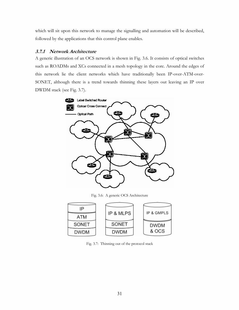
31
which will sit upon this network to manage the signalling and automation will be described,
followed by the applications that this control plane enables.
3.7.1 Network Architecture A generic illustration of an OCS network is shown in Fig. 3.6. It consists of optical switches
such as ROADMs and XCs connected in a mesh topology in the core. Around the edges of
this network lie the client networks which have traditionally been IP-over-ATM-over-
SONET, although there is a trend towards thinning these layers out leaving an IP over
DWDM stack (see Fig. 3.7).
Fig. 3.6: A generic OCS Architecture
Fig. 3.7: Thinning out of the protocol stack
32
3.7.2 Control Plane The control plane is the set of entities that controls and organizes the links between the
network elements, determining the paths to other nodes in the network. The optical layer
needs a large amount of human intervention for any type of modification. Currently, even
the most basic functions, such as link and neighbour discovery, are either manually
implemented or depend on non-standard protocol, which prevents interoperability between
carriers. Provisioning a new circuit proves very inefficient in terms of cost and time.
Network service providers and vendors have attempted to overcome this deficiency by
developing a standard for the optical control plane under the guidance of the International
Telecommunications Union Telecommunications Standardization sector (ITU-T), the
Internet Engineering Task Force (IETF) and the Optical Internetworking Forum (OIF). The
general scope of the three standardization bodies is to develop an optical control plane
capable of creating dynamic optical links triggered by user or management requests. In [26]
the authors present a review of the standardization activity of the above cited bodies,
emphasizing the interoperability aspects of their work.
ITU-T ASON The Automatically Switched Optical Network (ASON) [27] is a control plane architecture
being developed by the Study Group 15 of the ITU-T. It is not a protocol or a suite of
protocols; rather it is an architecture which defines components in the control plane and the
interactions between these components and those of the transport plane and management
plane. ASON defines the requirements for an optical network capable of new functionalities
like link and neighbour discovery, user interaction and fast dynamic provisioning of
lightpaths, allowing the user to request bandwidth on-demand, and to reduce the bandwidth
allocation time to the order of seconds.
The control plane supports connections requested either by users or by network
management and is responsible for planning the route and signalling. It receives information
from the transport plane regarding signal quality, faults etc and uses this data for
provisioning and restoration.
Having a telecommunication-oriented background, the ITU-T group, has shaped its optical
architecture more from concepts derived from standards such as SDH, ISDN and ATM
than from the Internet protocols [28].

33
IETF GMPLS The IETF has a more interactive approach to the development of Generalized Multi-
Protocol Label Switching (GMPLS). In contrast to the ITU-T, where there is a designated
group proposing and evaluating ideas for the protocol development, the IETF work group
exchanges opinions with any Internet user who may want to actively participate to the
discussions through an Internet mailing list.
GMPLS [29] is derived from Multi Protocol Label Switching (MPLS) [30], a technique that
allows traffic engineering by creating switched virtual circuits through an IP network. Each
time a packet enters a label-switched path it is marked with a label (similar to a packet
header) which indicates the downstream neighbour to which the packet should be switched.
After reading the label attached to the packet, this downstream neighbour replaces it with a
new label that indicates to the subsequent downstream neighbour which route should be
taken. This process continues until the packets reach the end of the circuit switched path.
The practical advantages are that the short labels allow faster switching and cost reduction at
the hardware level and that traffic engineering can be implemented without affecting the
stability of the IP layer.
GMPLS extends this approach such that where MPLS could only accept packet switching
capable interfaces, GMPLS can accept each of the following:
1. Packet Switch Capable (PSC) interfaces such as IP Routers which switch packets
by reading information located in the packet header.
2. Layer-2 Switch Capable (L2SC) interfaces such as Ethernet and ATM switches
which are able to switch frames or cells.
3. Time-Division Multiplex Capable (TDM) interfaces which switch data depending
on it’s time slot (for example SONET/SDH DCSs)
4. Lambda Switch Capable (LSC) interfaces such as WSXCs or WIXCs which
switch optical signals with the granularity of a wavelength
5. Fiber-Switch Capable (FSC) interfaces such as FXC which switch the full
contents of a fiber.
Aside from control plane architecture definitions, GMPLS also defines a suite of protocols
which can be used on transport network architectures based either on the ASON overlay
34
network or its own GMPLS overlay or peer networks. Details of the GMPLS protocols are
beyond the scope of this work but are described in detail in references [31-37]. While both
networks can use very similar GMPLS protocols as an Internal Network to Network
Interface (I-NNI) protocol, their User Network Interface (UNI) protocols are different from
each other. Because different carriers use different GMPLS network architectures, a GMPLS
based External Network to Network Interface (E-NNI) protocol has been introduced so
that carriers/service providers can provide a seamless end-to-end call set up service between
different architectures.
OIF UNI/NNI ASON and GMPLS should be seen as complementary rather than competing technologies
despite the fact that some of the literature suggests otherwise [28]. The OIF is a
contribution-driven industry forum that encourages the cooperation between manufacturers,
users and service providers. The OIF is generally recognized as a merging point between the
ITU-T and IETF work in the optical control plane because it implements concepts and
protocols defined by both the standardization bodies. For example the user network
interface (UNI) concept is part of the ASON architecture and refers to ITU-T optical
transport standards (as SONET/SDH); while it uses GMPLS signalling protocols and
implements a GMPLS auto-discovery mechanism.
In 2004, the OIF organized an Interoperability demonstration [38], to show a practical
implementation of the optical control plane, demonstrating the feasibility of their approach
in a worldwide scale. The test brought together 15 vendors and 7 international carriers,
connecting different laboratories located all over the world through trans-oceanic optical
links and demonstrated the possibility of creating switched connections spanning multiple
architectures. It represented the first real test of the automatic control plane standardization
and its success helped to generate trust in an area that was viewed with scepticism by many
service providers.
Since then many field trials and interoperability demonstrations have been conducted but
carriers have only begun to deploy GMPLS recently. In late 2007 Verizon launched the
United States’ first bandwidth on demand service [39] which is run on a GMPLS network.

35
3.7.3 Applications The applications which can be enabled and enhanced [40] through automatically and
manually switched optical circuits in transparent optical networks are described below.
Network Management ‘Point and click’ centralized network management [41,42] significantly reduces a carrier’s
(OpEx) because it removes the need for an engineer to visit every site on the path in order
to install the correct fixed wavelength components needed to re-arrange the network. If new
wavelengths are required then only the end nodes need to be visited to install new
transponders; if the wavelengths are already present, but need reconfiguring then no site
visits are required at all.
Bandwidth Provisioning Until recently, if a service provider for example, requested more bandwidth from a carrier,
the delivery time ranged between a number of days and a number of weeks. With OCS
enabled by GMPLS, this delivery time has been reduced to hours or even minutes. In
addition, because traffic demand is generally quite predictable over weeks or months,
bandwidth can be scheduled in advance in response to these predictable demands [39].
Traffic Management A GMPLS control plane allows network managers to centrally re-route a portion of the
traffic in the event of congestion for example [43]. Note that this is in response to real time
events as opposed to network management mentioned above which would be in response to
longer term trends.
Protection and Restoration In today’s world, reliable transfer of data is vital. Carriers often guarantee almost constant
(99.999%) network up-time in their Service Level Agreements (SLAs) and failure to maintain
such uptime can lead to financial penalties or loss of business. Nevertheless, failures do
occur due to human error (e.g. fiber cuts) or equipment faults (e.g. amplifier fault).
Heretofore, protection has often been provided by a dedicated protection fiber which would
be automatically switched into place in the event of a failure [44]. This practice is highly
inefficient because the maximum resource usage available with such a scheme is 50%. In
other methods, the protection is shared by a number of resources [44,45]. For example, one
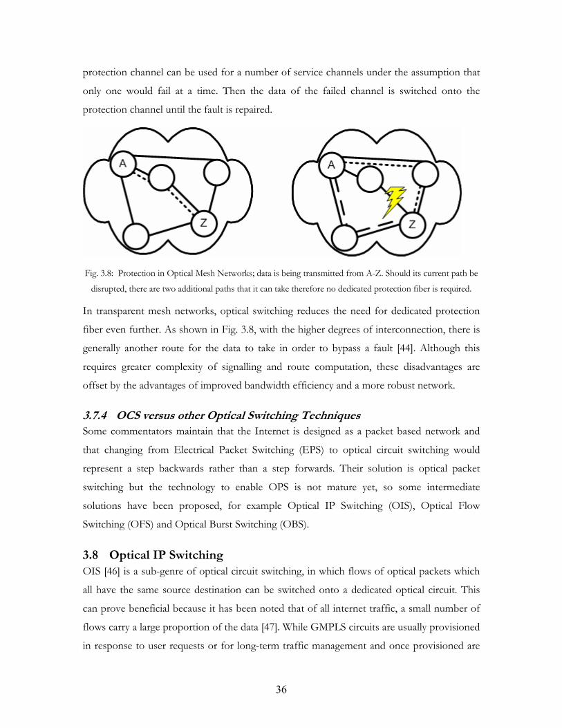
36
protection channel can be used for a number of service channels under the assumption that
only one would fail at a time. Then the data of the failed channel is switched onto the
protection channel until the fault is repaired.
Fig. 3.8: Protection in Optical Mesh Networks; data is being transmitted from A-Z. Should its current path be
disrupted, there are two additional paths that it can take therefore no dedicated protection fiber is required.
In transparent mesh networks, optical switching reduces the need for dedicated protection
fiber even further. As shown in Fig. 3.8, with the higher degrees of interconnection, there is
generally another route for the data to take in order to bypass a fault [44]. Although this
requires greater complexity of signalling and route computation, these disadvantages are
offset by the advantages of improved bandwidth efficiency and a more robust network.
3.7.4 OCS versus other Optical Switching Techniques Some commentators maintain that the Internet is designed as a packet based network and
that changing from Electrical Packet Switching (EPS) to optical circuit switching would
represent a step backwards rather than a step forwards. Their solution is optical packet
switching but the technology to enable OPS is not mature yet, so some intermediate
solutions have been proposed, for example Optical IP Switching (OIS), Optical Flow
Switching (OFS) and Optical Burst Switching (OBS).
3.8 Optical IP Switching OIS [46] is a sub-genre of optical circuit switching, in which flows of optical packets which
all have the same source destination can be switched onto a dedicated optical circuit. This
can prove beneficial because it has been noted that of all internet traffic, a small number of
flows carry a large proportion of the data [47]. While GMPLS circuits are usually provisioned
in response to user requests or for long-term traffic management and once provisioned are
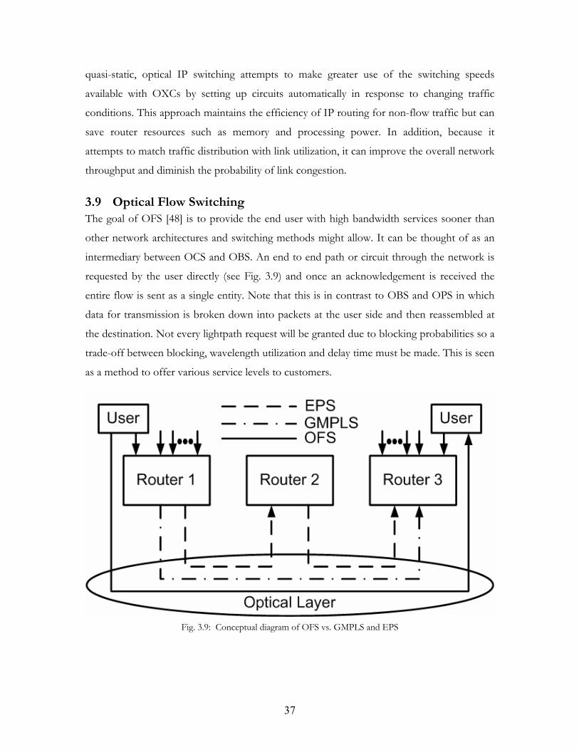
37
quasi-static, optical IP switching attempts to make greater use of the switching speeds
available with OXCs by setting up circuits automatically in response to changing traffic
conditions. This approach maintains the efficiency of IP routing for non-flow traffic but can
save router resources such as memory and processing power. In addition, because it
attempts to match traffic distribution with link utilization, it can improve the overall network
throughput and diminish the probability of link congestion.
3.9 Optical Flow Switching The goal of OFS [48] is to provide the end user with high bandwidth services sooner than
other network architectures and switching methods might allow. It can be thought of as an
intermediary between OCS and OBS. An end to end path or circuit through the network is
requested by the user directly (see Fig. 3.9) and once an acknowledgement is received the
entire flow is sent as a single entity. Note that this is in contrast to OBS and OPS in which
data for transmission is broken down into packets at the user side and then reassembled at
the destination. Not every lightpath request will be granted due to blocking probabilities so a
trade-off between blocking, wavelength utilization and delay time must be made. This is seen
as a method to offer various service levels to customers.
Fig. 3.9: Conceptual diagram of OFS vs. GMPLS and EPS
38
Circuits which are provisioned generally last >100ms before being torn down. Such
timescales are short in comparison to typical GMPLS circuits but longer than typical data
Bursts (DBs) in OBS (100µs – 100ms). The minimum granularity is a wavelength, so if a user
does not have enough data to occupy a full wavelength, data from a number of users can be
aggregated. Because scheduling is used and an end to end path is reserved, neither buffering
nor contention resolution inside the network is required which can represent an advantage
over certain forms of OBS.
3.10 Optical Burst Switching OBS [49] is another method which has been proposed to bridge the gap between OCS and
OPS in the core network. Data in today’s networks is typically bursty in nature so in contrast
with OFS, in OBS the user’s data is ‘packetised’. While still in the electronic domain these
packets are then aggregated into bursts at the edge of the core network. Bursts are then
converted to optical form, and routed through the entire core network in the optical domain.
Only at the destination node it is converted to electrical domain. It is then disassembled, and
all the IP packets are sent to their respective destinations.
In circuit-switched networks, the path is only considered to be complete after the initiating
station has received positive acknowledgement, and no data can be sent before it happens.
The delay between request and acknowledgement is of little consequence if the average
length of connection is much greater than the required set-up time. Optical bursts, while
larger than packets, are still relatively small, and waiting for a positive acknowledgement
tends to be inefficient. Therefore, other switching protocols had to be developed.
There have been many different OBS schemes proposed in the literature but the two main
categories are those implemented as fast reconfigurable ‘packetised’ OCS and those
implemented with node-by-node routing where the route to the next node is decided at each
individual node. The latter scheme is similar to optical packet switching but with large
aggregated packets.
The fast OCS schemes can be further broken down into schemes with two way reservation
protocols such as tell-and-wait (TAW) [50] which wait for an acknowledgement before
sending the burst, and schemes with one-way reservation such as tell-and-go (TAG) which
send the burst regardless of whether the network is ready for it or not, thereby reducing
39
latency but increasing blocking or contention probability. Common TAG signalling schemes
include just-in-time (JIT) [51] or just-enough-time (JET) [52] Control signals are sent on a
separate wavelength ahead of the burst in time, to reserve the path between two nodes for
the duration of the burst. At each node they are converted to the electrical domain and
analyzed in order to make the routing decision. A major advantage of this method of OBS is
that optical buffers are not required inside the network.
In contrast, with the routed OBS [53], the latency is controlled and managed at each
intermediate node by including optical buffers based on fiber delay lines (FDLs) in the node.
This removes the need for pre-computation and estimation of the time it will take the burst
to travel through the network and improves scalability. Routed OBS uses optical labels to
control the switching and routing of bursts through the network and can work alongside
OCS and OPS based on label switching also. This interoperability may prove very beneficial
for supporting different services. Optical label switching will be discussed in greater detail in
the next section.
3.11 Optical Packet Switching Optical Packet Switching (OPS) is the forwarding of individual data packets one by one
through a network directly in the optical layer [54]. In currently deployed transport networks
the finest granularity which can be switched is a wavelength. Sub-wavelength traffic
grooming must be performed in the electrical domain using expensive and slow OEO
conversions. The main motivation for OPS is to allow more efficient use of the huge
bandwidth available by switching at the packet level in the optical domain. It is also
envisaged that optical packet switching may offer vastly reduced footprint and power
consumption over electrical packet switching [55].
While research in the area has been going on for a number of years, and testbeds and
demonstrators have emerged, the technology is far from being mature enough for
commercial deployment. Many major technological obstacles must be overcome including
the development of very high speed (nanosecond) switching fabrics, optical buffers,
wavelength conversion and 3R regeneration, header recognition and optical clock recovery.
Current systems generally combine optical and electrical technologies, with most of the
switching and transport being performed optically and the control and processing being
performed electrically.
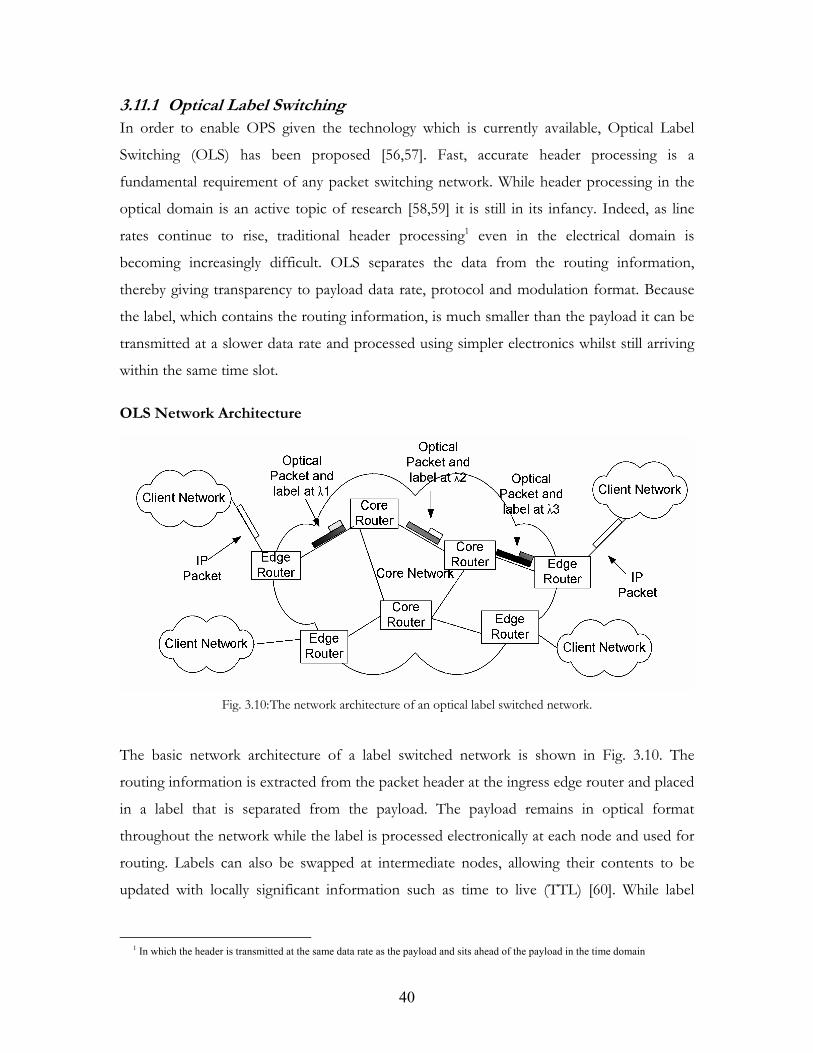
40
3.11.1 Optical Label Switching In order to enable OPS given the technology which is currently available, Optical Label
Switching (OLS) has been proposed [56,57]. Fast, accurate header processing is a
fundamental requirement of any packet switching network. While header processing in the
optical domain is an active topic of research [58,59] it is still in its infancy. Indeed, as line
rates continue to rise, traditional header processing1 even in the electrical domain is
becoming increasingly difficult. OLS separates the data from the routing information,
thereby giving transparency to payload data rate, protocol and modulation format. Because
the label, which contains the routing information, is much smaller than the payload it can be
transmitted at a slower data rate and processed using simpler electronics whilst still arriving
within the same time slot.
OLS Network Architecture
Fig. 3.10: The network architecture of an optical label switched network.
The basic network architecture of a label switched network is shown in Fig. 3.10. The
routing information is extracted from the packet header at the ingress edge router and placed
in a label that is separated from the payload. The payload remains in optical format
throughout the network while the label is processed electronically at each node and used for
routing. Labels can also be swapped at intermediate nodes, allowing their contents to be
updated with locally significant information such as time to live (TTL) [60]. While label
1 In which the header is transmitted at the same data rate as the payload and sits ahead of the payload in the time domain
41
swapping adds to the cost and complexity of each node, it allows for better network
scalability [57].
OLS Node Architecture A generic OLS node architecture is shown in Fig. 3.11. A number of input fibers each
carrying optical packets on various wavelengths are demultiplexed into separate wavelengths
and sent to the input interface, where the label information is extracted and sent to the
switch controller. The switch controller analyses the label information, and adjusts the
switch fabric as necessary to route the packet (which may involve buffering or wavelength
conversion to avoid contention). If label swapping is used a new label is computed and
passed to the output interface where it is attached to the payload. Packets on individual
wavelengths are then re-multiplexed onto an output fiber and forwarded to the next node.
Fig. 3.11: A generic optical packet switching node architecture
Label Coding The three most widely studied label coding techniques reported in the literature are bit-serial,
subcarrier multiplexed and orthogonal [61]. Other techniques include WDM labelling and
optical code division multiplexed (OCDM) labelling with the latter receiving a lot of interest
in recent years. Fig. 3.12 shows a basic representation of the three main coding techniques
and brief descriptions are given below. The labelling techniques will be discussed in greater
detail in Chapter 6 and because sub-carrier labelling is the method employed in the OPS
section of this work it will receive the greatest attention
42
Fig. 3.12: Common Optical Label Coding Techniques
Bit serial labelling: In this technique the label is placed ahead of the payload in the time
domain and on the same wavelength with guard bands in between [62, 63]. While this
method is free from crosstalk between the payload and label which the other two methods
suffer from, the main disadvantage associated with it is the strict timing required.
Subcarrier Multiplexed labelling: Here, the label data is modulated onto an RF sub-
carrier, which is then combined with the optical carrier either optically [64], electro optically
[65] or electrically [66, 67]. Simplicity and the lack of tight timing requirements are the main
advantages of SCM labelling, while crosstalk, reduced spectral efficiency and dispersion
induced fading are the major demerits.
Orthogonal labelling: The payload and label data are modulated onto different dimensions
of the optical carrier in this method. For example the payload could be modulated onto the
intensity of the light while the label is modulated onto the frequency or phase [68]. Like
SCM labelling, crosstalk between label and payload is an issue and the receiver required is
more complicated than that of SCM. However, the channel bandwidth remains the same
even after the label is added giving better spectral efficiency.
3.11.2 Technology to Enable Optical Packet Switching In this section some of the technologies which will be required to enable optical packet
switching to be commercially realised are discussed.
43
Optical Buffering Buffering is a vital function in a packet switching node. A fixed length buffer is required to
store the data while the header information is read. Variable length buffers are required in
switches to store data if resources are not available to serve them immediately. In electronic
switches, the buffers may be in the form of Random Access Memory (RAM) which is useful
because it can store information indefinitely and the information can be called on at any
time. In the optical domain, however, this luxury is not available due to the fact that light
cannot be stopped and stored. Instead it must be delayed by a certain amount of time. Fiber
Delay Lines (FDLs) are the most widely used optical buffering technique at the moment. In
general, groups of FDLs with different lengths are used to create variable delay lines [69] as
shown in Fig. 3.13. Slow light waveguides are a possible alternative to FDLs. These devices
can reduce the speed of light to a fraction of its usual speed [70]. Both methods are bulky
and impractical as a direct replacement for current sized electronic buffers however recent
work suggests that buffer sizes can be significantly reduced without impacting network
throughput [71].
Fig. 3.13: Fiber delay lines used to create variable length optical buffer; the arrayed waveguide grating router
(AWGR) routes the packet to the appropriate delay line depending on the wavelength of the packet which is
set by the tunable wavelength converters (TWCs)
Fast Switching As mentioned previously, switch fabrics for optical packet switching must have switching
times of the order of a few nanoseconds. They also must be easily scalable and display
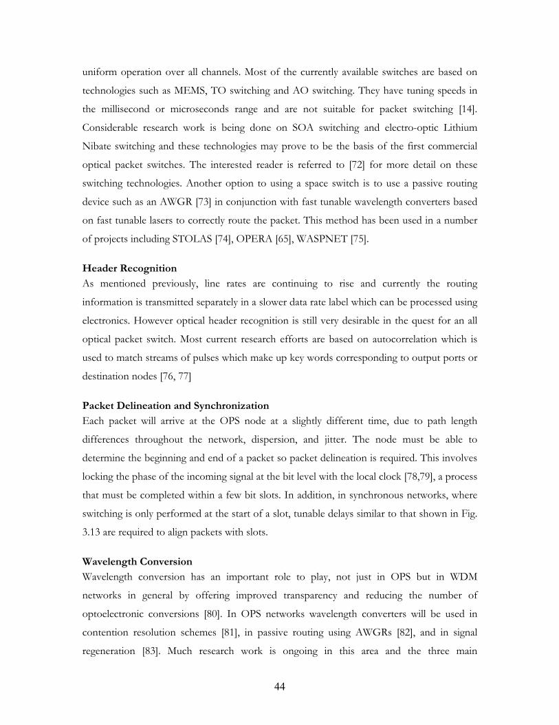
44
uniform operation over all channels. Most of the currently available switches are based on
technologies such as MEMS, TO switching and AO switching. They have tuning speeds in
the millisecond or microseconds range and are not suitable for packet switching [14].
Considerable research work is being done on SOA switching and electro-optic Lithium
Nibate switching and these technologies may prove to be the basis of the first commercial
optical packet switches. The interested reader is referred to [72] for more detail on these
switching technologies. Another option to using a space switch is to use a passive routing
device such as an AWGR [73] in conjunction with fast tunable wavelength converters based
on fast tunable lasers to correctly route the packet. This method has been used in a number
of projects including STOLAS [74], OPERA [65], WASPNET [75].
Header Recognition As mentioned previously, line rates are continuing to rise and currently the routing
information is transmitted separately in a slower data rate label which can be processed using
electronics. However optical header recognition is still very desirable in the quest for an all
optical packet switch. Most current research efforts are based on autocorrelation which is
used to match streams of pulses which make up key words corresponding to output ports or
destination nodes [76, 77]
Packet Delineation and Synchronization Each packet will arrive at the OPS node at a slightly different time, due to path length
differences throughout the network, dispersion, and jitter. The node must be able to
determine the beginning and end of a packet so packet delineation is required. This involves
locking the phase of the incoming signal at the bit level with the local clock [78,79], a process
that must be completed within a few bit slots. In addition, in synchronous networks, where
switching is only performed at the start of a slot, tunable delays similar to that shown in Fig.
3.13 are required to align packets with slots.
Wavelength Conversion Wavelength conversion has an important role to play, not just in OPS but in WDM
networks in general by offering improved transparency and reducing the number of
optoelectronic conversions [80]. In OPS networks wavelength converters will be used in
contention resolution schemes [81], in passive routing using AWGRs [82], and in signal
regeneration [83]. Much research work is ongoing in this area and the three main
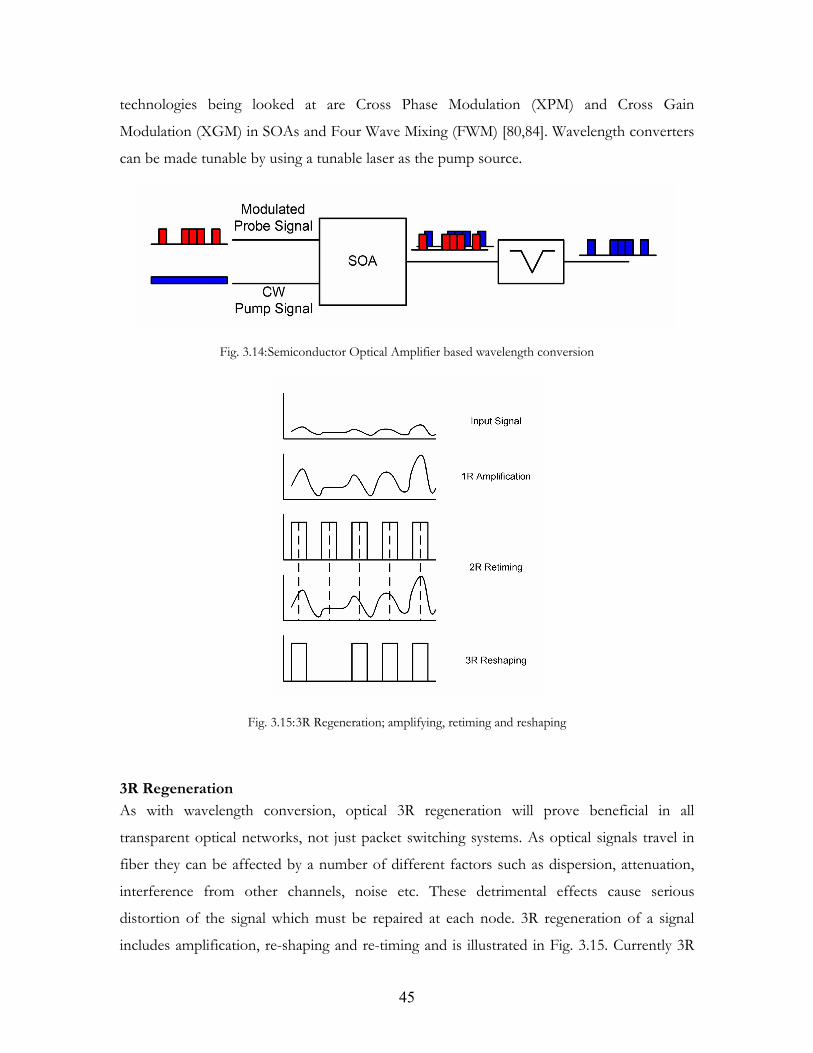
45
technologies being looked at are Cross Phase Modulation (XPM) and Cross Gain
Modulation (XGM) in SOAs and Four Wave Mixing (FWM) [80,84]. Wavelength converters
can be made tunable by using a tunable laser as the pump source.
Fig. 3.14: Semiconductor Optical Amplifier based wavelength conversion
Fig. 3.15: 3R Regeneration; amplifying, retiming and reshaping
3R Regeneration As with wavelength conversion, optical 3R regeneration will prove beneficial in all
transparent optical networks, not just packet switching systems. As optical signals travel in
fiber they can be affected by a number of different factors such as dispersion, attenuation,
interference from other channels, noise etc. These detrimental effects cause serious
distortion of the signal which must be repaired at each node. 3R regeneration of a signal
includes amplification, re-shaping and re-timing and is illustrated in Fig. 3.15. Currently 3R
46
regeneration is performed in the electrical domain with expensive OEO conversions
required for each channel. SOA based MZIs have been used to demonstrate optical 3R
regeneration but the technology is not yet mature [85].
3.12 Conclusion This chapter reviewed a number of optical switching techniques and discussed the
components and technologies required to enable them. In the remaining chapters,
experimental work in the areas of OCS and OPS will be covered in detail. Chapter 4 will
discuss work carried out at which focuses on issues relating to slow reconfiguration, typical
of OCS. In Chapter 5, experimental work carried out on one of the primary enabling
technologies for OPS, namely the Fast Tunable Laser (FTL) will be detailed, while Chapter 6
describes experiments which analyze a particular OPS transmitter built using FTLs, which
was designed within the confines of this work.
47
References [1] O. Leclerc, B. Lavigne, D. Chiaroni, E. Desuivre, “All Optical Regeneration:
Principles and WDM Implementation” in Optical Fibre Telecommunications IVA, (I. Kaminov,
T. Li., eds), San Diego, Academic Press, 2002, pp 732 – 783.
[2] Shoa-Kai Liu, "Challenges of all-optical network evolution," Lasers and Electro-Optics
Society Annual Meeting, 1998. LEOS '98. IEEE , vol.1, no., pp.182-183 vol.1, 1-4 Dec 1998
[3] O. Leclerc, "Towards transparent optical networks: still some challenges ahead,"
Lasers and Electro-Optics Society, 2005. LEOS 2005. The 18th Annual Meeting of the IEEE , vol.,
no., pp. 418-419, 22-28 Oct. 2005
[4] J. Strand, “Optical Network Architecture Evolution” in Optical Fibre
Telecommunications IVB, (I. Kaminov, T. Li., eds), San Diego, Academic Press, 2002, pp 57 –
153.
[5] O. Turkcu, S. Subramaniam, "Blocking in Reconfigurable Optical Networks,"
INFOCOM 2007. 26th IEEE International Conference on Computer Communications. IEEE , vol.,
no., pp.188-196, 6-12 May 2007
[6] M. O’Mahony, “Future Optical Networks” in Optical Fibre Telecommunications VB, (I.
Kaminov, T. Li., A. Willner eds), San Diego, Academic Press, 2008, pp 611 – 640.
[7] M. Feuer, D. Kilper, S. Woodward, “ROADMs and their system applications” in
Optical Fibre Telecommunications VB, (I. Kaminov, T. Li., A. Willner eds), San Diego, Academic
Press, 2008, pp 293 – 343.
[8] F. Smyth, B. Roycroft, B. Corbett, P. Lambkin, and L. P. Barry, “Fast wavelength
switching lasers using two-section slotted Fabry-Pérot structures,” IEEE Photon. Technol.
Lett., vol. 18, no. 20, pp. 2105–2107, Oct. 2006.
[9] J.E. Simsarian, et al, “Less than 5-ns Wavelength Switching with an SG-DBR Laser”,
IEEE Photonics Technology Letters, vol 18, pp 565-567, Feb 2006.
[10] D. Cavendish, "Evolution of optical transport technologies: from SONET/SDH to
WDM," Communications Magazine, IEEE , vol.38, no.6, pp.164-172, Jun 2000
48
[11] J-F. Labourdette, E. Bouillet, C. Olszewski, “Operational Aspects of Mesh
Networking in WDM Optical Netwoks” in Emerging Optical Network Technologies: Architectures,
Protocols and Performance, (K.M Sivalingam, S. Subramaniam, eds), New York, Spring Science
& Business Media, 2005, pp 219 – 241.
[12] S. Chandrasekhar, D. Kilper, “Using testbeds for optically-transparent mesh network
experimentation” Lasers & Electro-Optics Society, IEEE Oct. 2006 Page(s):771 – 772
[13] T. S. El-Bawab, Optical Switching,, New York, Springer Science and Business Media,
2006, pp 333 – 379
[14] Ma Xiaohua, Kuo Geng-Sheng, "Optical switching technology comparison: optical
MEMS vs. other technologies," Communications Magazine, IEEE , vol.41, no.11, pp. S16-S23,
Nov. 2003
[15] R.A Jensen, "Comparison of optical switching technologies for intelligent optical
networks," Lasers and Electro-Optics Society, 2001. LEOS 2001. The 14th Annual Meeting of the
IEEE , vol.1, no., pp.230-231 vol.1, 2001
[16] R.S Weis, T.K Gaylord, “Lithium Niobate: Summary of Physical Properties and
Crystal Structure,” Appl. Physics A., Vol. 37, No. 4, pp. 191-203, 1985.
[17] I. Bennion, L. Thylen, N. F. Whitehead, "Electro-optic switching systems,"
Communications, 1990. ICC '90, Including Supercomm Technical Sessions. SUPERCOMM/ICC '90.
Conference Record., IEEE International Conference on , vol., no., pp.1130-1134 vol.3, 16-19 Apr
1990
[18] T. Kato, T. Shimizu, T. Tamanuki, "Hybrid-integrated SOAG array module for
photonic packet switching application," Lasers and Electro-Optics Society, 2001. LEOS 2001. The
14th Annual Meeting of the IEEE , vol.2, no., pp.847-848 vol.2, 2001
[19] A. Yariv, P. Yeh, “Optical Waves in Crystals”, John Wiley and Sons, 1984
[20] W.J. Tomlinson, R.E. Wagner, A.R Strnad, F. A. Dunn, F.A., "Multiposition optical-
fibre switch," Electronics Letters , vol.15, no.6, pp.192-194, March 15 1979
49
[21] S. Hengstler, J.J. Uebbing, P. McGuire, "Laser-activated optical bubble switch
element," Optical MEMS, 2003 IEEE/LEOS International Conference on , vol., no., pp. 117-118,
18-21 Aug. 2003
[22] A.V. Uskov, E.P. O'Reilly, R.J. Manning, R.P. Webb, D. Cotter; M. Laemmlin, N.N.
Ledentsov, D. Bimberg, "On ultrafast optical switching based on quantum-dot
semiconductor optical amplifiers in nonlinear interferometers," Photonics Technology Letters,
IEEE , vol.16, no.5, pp.1265-1267, May 2004
[23] I. White, R. Penty, M. Webster, Yew Jun Chai, A. Wonfor, S. Shahkooh,
"Wavelength switching components for future photonic networks," Communications Magazine,
IEEE , vol.40, no.9, pp. 74-81, Sep 2002
[24] T. S. El-Bawab, “Optical Switching in Communications Networks” in Optical
Switching, (T. S. El-Bawab, ed), New York, Springer Science and Business Media, 2006, pp
333 – 379
[25] M. Zirnigibl, “Applications for Optical Switch Fabrics” in Optical Fibre
Telecommunications IVA, (I. Kaminov, T. Li., eds), San Diego, Academic Press, 2002, pp 374 –
404.
[26] D. Saha, B. Rajagopalan, G. Bernstein. “'The Optical Network Control Plane: State
of the Standards and Deployment”. IEEE Communications Magazine, Vol. 41, Issue: 8 , Aug.
2003
[27] “Architecture for the automatically switched optical network (ASON)”. ITU-T Rec.
G.8080.
[28] N. Larkin. “ASON AND GMPLS – The battle of the optical control plane”. White
paper, Data Connection, July 2004
[29] E. Mannie et al. “Generalized Multi-Protocol Label Switching (GMPLS)
Architecture”. IETF RFC 3945, Oct 2004
[30] E. Rosen et al. “Multiprotocol Label Switching Architecture”. IETF RFC 3031, Jan
2001
50
[31] L. Berger et al. Generalized Multi-Protocol Label Switching (GMPLS) Signaling
Resource ReserVation Protocol-Traffic Engineering (RSVP-TE) Extensions. IETF RFC
3473, Jan 2003.
[32] L. Berger et al. “Generalized Multi-Protocol Label Switching (GMPLS) Signaling
Constraint-based Routed Label Distribution Protocol (CR-LDP) Extensions”. IETF RFC
3472, Jan 2003.
[33] L. Andersson et al. “LDP Specification”. IETF RFC 3036, Jan 2001
[34] R. Braden et al. “Resource ReSerVation Protocol (RSVP)--Version 1 Functional
Specification”. IETF RFC 2205, Sep 1997.
[35] K. Kompella et al. “OSPF Extensions in Support of Generalized Multi-Protocol
Label Switching”. IETF RFC 4203, Oct 2005.
[36] J. Lang, et al. “Link Management Protocol (LMP)”. IETF RFC 4204, Oct 2005.
[37] A. Fredette et al. “Link Management Protocol (LMP) for Dense Wavelength Division
Multiplexing (DWDM) Optical Line Systems”. IETF RFC 4209, Oct.2005
[38] J.D. Jones, L. Ong,, M.A. Lazer. “Creating an Intelligent Optical Network
Worldwide Interoperability Demonstration”. IEEE Communications Magazine, Vol. 42, Issue
11, Nov. 2004.
[39] Liu, S. Lily Chen, “Deployment of Carrier-Grade Bandwidth-on-Demand Services
over Optical Transport Networks: A Verizon Experience” Optical Fiber Communication and the
National Fiber Optic Engineers Conference, 2007. OFC/NFOEC 2007. Conference on 25-29 March
2007 Page(s):1 – 8
[40] A. Banerjee, J. Drake, J. P. Lang, B. Turner, K. Kompella, Y. Rekhter, "Generalized
multiprotocol label switching: an overview of routing and management enhancements,"
Communications Magazine, IEEE , vol.39, no.1, pp.144-150, Jan 2001
[41] www.polarisnetworks.com/images/PDF/GMPLSWhitePaperComplete.pdf
[42] “Optical Signalling Systems: Who’s doing what?” Light Reading, Jan 08, 2002
51
[43] D. Shimazaki, E. Oki, K. Shiomoto, "Multi-layer Traffic Engineering Experimental
System in IP Optical Network," High Performance Switching and Routing, 2007. HPSR '07.
Workshop on , vol., no., pp.1-6, May 30 2007-June 1 2007
[44] S. Ramamurthy, L. Sahasrabuddhe, B. Mukherjee, "Survivable WDM mesh
networks," Lightwave Technology, Journal of , vol.21, no.4, pp. 870-883, April 2003
[45] D. Elie-Dit-Cosaque, M. Ali, L. Tancevski, "Informed dynamic shared path
protection," Optical Fiber Communication Conference and Exhibit, 2002. OFC 2002 , vol., no., pp.
492-493, 17-22 Mar 2002
[46] G. Mulvihill; M. Ruffini; F. Smyth; L. Barry; L. Doyle; D. O'Mahony, "Optical IP
Switching a Solution to Dynamic Lightpath Establishment in Disaggregated Network
Architectures," Transparent Optical Networks, 2006 International Conference on , vol.3, no., pp.78-
81, June 2006
[47] W. Fang, L. Peterson, "Inter-AS traffic patterns and their implications" Global
Telecommunications Conference, GLOBECOM '99 3, Pages: 1859-1868
[48] V. W. S. Chan, G. Weichenberg, and M. Medard, "Optical Flow Switching,"
Proceedings of Workshop on Optical Burst Switching (WOBS 2006), San Jose, (Invited
Paper) October 2006
[49] C. Qiao, M. Yoo, “Optical burst switching (OBS) – A new paradigm for an optical
internet ” Journal of High Speed Networks, Vol. 8, No. 1, pp 3-16,1999.
[50] M. Duser, P. Bayvel, “Performance of a dynamically wavelength routed optical burst
switched network”, IEEE Photon. Technol. Lett., 14, 239-241, 2002.
[51] J.Y. Wei, R.I. McFarland, Jr., "Just-in-time signaling for WDM optical burst
switching networks," Lightwave Technology, Journal of , vol.18, no.12, pp.2019-2037, Dec 2000
[52] Myungsik Yoo; Chunming Qiao, "Just-Enough-Time (JET): a high speed protocol
for bursty traffic in optical networks," Vertical-Cavity Lasers, Technologies for a Global Information
Infrastructure, WDM Components Technology, Advanced Semiconductor Lasers and Applications,
Gallium Nitride Materials, Processing, and Devi , vol., no., pp.26-27, 11-15 Aug 1997
52
[53] S.J.B. Yoo, Hyuek Jae Lee, S. Vaidianathan, K. Okamoto, S. Kamei, "Optical-label
switching and routing by rapidly tunable wavelength conversion and uniform loss cyclic
frequency array-waveguide grating," Optical Fiber Communication Conference and Exhibit, 2001.
OFC 2001 , vol.3, no., pp. WDD49-1-WDD49-3 vol.3, 2001
[54] “Special Issue on Photonic Packet Switching Systems, Technology and Techniques”,
Journal of Lightwave Technology, December 1998
[55] S. J. B. Yoo, "Advanced optical components for next-generation photonic
networks," Proc. SPIE 5246, 224-234 (2003)
[56] F. Xue, S. J. B. Yoo, “High Capacity Multiservice Optical Label Switching for The
Next Generation Internet”, IEEE Optical Communications, May 2004
[57] S. J. B Yoo, “Optical Label Switching, MPLS, MPLambdaS and GMPLS”. Optical
Networks Magazine, May/June 2003, p 17-31
[58] M. C. Cardakli, S. Lee, A. E. Willner, V. Grubsky, D. Starodubov, and J. Feinberg,
“Reconfigurable optical packet header recognition and routing using time-to-wavelength
mapping and tunable fiber Bragg gratings for correlation decoding,” IEEE Photon. Technol.
Lett., vol. 12, no. 5, pp. 552–554, May 2000.
[59] Hyun-Do Jung; Monroy, I.T.; Koonen, A.M.J.; Tangdiongga, E., "All-Optical Data
Vortex Node Using an MZI-SOA Switch Array," Photonics Technology Letters, IEEE , vol.19,
no.22, pp.1777-1779, Nov.15, 2007
[60] B. Meagher et al, “Design and implementation of ultra-low latency optical label
switching for packet-switched WDM networks”. Journal of Lightwave Technology, Vol 18,
Iss 12, Dec 2000 pp 1978 – 1987
[61] D.J. Blumenthal, et al “All-optical label swapping networks and technologies”,
Journal of Lightwave Technology, Vol 18, Iss 12, Dec 2000, pp 2058 – 2075
[62] W. Wang, L. G. Rau, D. J. Blumenthal, “160Gb/s Variable Length Packet/ 10Gb/s
Label All Optical Label Switching with Wavelength Conversion and Unicast/Multicast
Operation”,. Journal of Lightwave Technology, Vol 23, Iss 1, Jan 2005 pp 211 – 218
53
[63] J. J. V. Olmos, I. T. Monroy, A. M. J. Koonen, “All Optical Label and Payload
Separator for a Time-Serial RZ-IM/IM Scheme”, IEEE Photonics Technology Letters, vol
18, Iss 3, pp 496-498
[64] T. Dimmick, R. Doshi, R. Rajaduray, D. Blumenthal, “Optically Multiplexed
Transmitter for hybrid baseband and subcarrier multiplexed signals”. 26th European
Conference on Optical Communication, 1996. ECOC '00. Vol 2, 3-7 Sept. 200 pp 155 - 156
[65] A. Carena, M. D. Vaughn, R. Gaudino, M Shell, D. J. Blumenthal, “OPERA: An
Optical Packet Experimental Routing Architecture with Label Swapping Capability”, Journal
of Lightwave Technology, Vol. 16, Iss. 12, pp 2135-2145
[66] S.J.B. Yoo, H. J. Lee, Z. Pan, J. Cao, Y. Zhang, K. Okamoto, S. Kamei, “Rapidly
Switching All Optical Packet Routing System with Optical Label Sapping incorporating
tunable wavelength conversion and a Uniform Loss cyclic frequency AWGR”, IEEE
Photonics Technology Letters, vol 13, Iss 6, pp 635-637
[67] Z. Zhu et al, “RF Photonics Signal Processing in Subcarrier Multiplexed Optical-
Label Switching Communication Systems”, IEEE Journal of Lightwave Technology, vol 21,
Iss. 12, pp 3155-3166
[68] T. Koonen, G. Morthier, J. Jennen, H. de Waardt, P. Demeester, “Optical packet
routing in IP-over-WDM networks deploying two-level optical labeling” 27th European
Conference on Optical Communication, 2001. ECOC '01. Vol 4, 30 Sept - 4 Oct. 2001 pp
608 - 609
[69] H. Yang, S.J.B. Yoo, “All-optical variable buffering strategies and switch fabric
architectures for future all-optical data routers” Journal of Lightwave Technology, Vol 23,
Iss 10, Oct. 2005 pp 3321 – 3330
[70] R.S. Tucker, P.-C.Ku, C.J. Chang-Hasnain, “Slow-Light Optical Buffers: Capabilities
and Fundamental Limitations”, Journal of Lightwave Technology, Vol 23, Iss 12, Dec.
2005 pp 4046 - 4066
[71] N. Beheshti, Y. Ganjali, R. Rajaduray, D. Blumenthal, N. McKeown, “Buffer sizing
in all-optical packet switches” Optical Fiber Communication Conference 2006, OFC 2006
and the 2006 National Fiber Optic Engineers Conference 5-10 March 2006
54
[72] G.I. Papadimitriou, C. Papazoglou, A.S. Pomportsis, “Optical switching: switch
fabrics, techniques, and architectures” Journal of Lightwave Technology, Vol 21, Iss 2, Feb.
2003 pp 384 – 405
[73] M.C. Chia, et al “Packet loss and delay performance of feedback and feed-forward
arrayed-waveguide gratings-based optical packet switches with WDM inputs-outputs”
Journal of Lightwave Technology, Vol 19, Iss 9, Sept. 2001 pp 1241 – 1254
[74] K.G. Vlachos, I.T. Monroy, A.M.J Koonen, C. Peucheret, P. Jeppesen, “STOLAS:
switching technologies for optically labeled signals” IEEE Communications Magazine, Vol
41, Iss 11, Nov. 2003 pp S9 – 15
[75] D.K. Hunter, et al "WASPNET: a wavelength switched packet network,"
Communications Magazine, IEEE , vol.37, no.3, pp.120-129, Mar 1999
[76] H.J.S. Dorren, et al “Optical packet switching and buffering by using all-optical
signal processing methods”, Journal of Lightwave Technology, Vol 21, Iss 1, Jan 2003 pp.
2-12
[77] J. M. Martinez, J. Herrera, F. Ramos, J. Marti, “All-Optical Address Recognition
Scheme for Label Swapping Networks”. IEEE Photonics Technology Letters, vol 18, Iss 1,
pp 151-153
[78] L. Zucchelli, M. Burzio, P. Gambini, “For optical packet delineation and in optical
packet switched networks” 22nd European Conference on Optical Communication, 1996.
ECOC '96. Vol 3, 15-19 Sept. 1996 pp 301 - 304
[79] C. Guillemot, et al “Optical packet switch demonstrator assessment: packet
delineation and fast wavelength routing” 23rd European Conference on Optical Fibre
Communications, Vol 3, 22-25 Sept. 1997 pp 343 - 346
[80] J.M.H. Elmirghani, H.T. Mouftah, “All-optical wavelength conversion: technologies
and applications in DWDM networks”, IEEE Communications Magazine, Vol 38, Iss 3,
Mar 2000 pp 86 – 92
55
[81] S. Rangarajan, Zhaoyang Hu; L. Rau, D.J. Blumenthal, “All-optical contention
resolution with wavelength conversion for asynchronous variable-length 40 Gb/s optical
packets, IEEE Photonics Technology Letters, Vol 16, Iss 2, Feb. 2004 pp 689 – 691
[82] D. Klonidis, C.T. Politi, R. Nejabati, M.J.O'Mahony, D. Simeonidou, “OPSnet:
design and demonstration of an asynchronous high-speed optical packet switch” Journal of
Lightwave Technology, Vol 23, Iss 10, Oct. 2005 pp 2914 – 2925
[83] S. Hojfeldt, S. Bischoff, J. Mork, “All-optical wavelength conversion and signal
regeneration using an electroabsorption modulator”, Journal of Lightwave Technology, Vol
18, Iss 8, Aug. 2000 pp 1121 – 1127
[84] D. Nesset, T. Kelly, D. Marcenac, “All-optical wavelength conversion using SOA
nonlinearities” IEEE Communications Magazine, Vol 36, Iss 12, Dec. 1998 pp 56 – 61
[85] M. Funabashi, Zuqing Zhu; Zhong Pan; S.J.B Yoo, L. Paraschis, “All-optical 3R
regeneration in monolithic SOA-MZI to achieve 0.4 million km fiber transmission” 18th
Annual Meeting of the IEEE Lasers and Electro-Optics Society, 2005. LEOS 2005. 23-27
Oct. 2005 pp 137 – 138
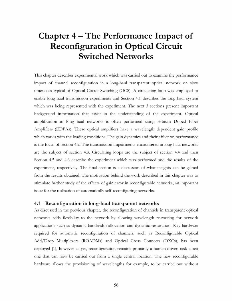
56
Chapter 4 – The Performance Impact of Reconfiguration in Optical Circuit
Switched Networks
This chapter describes experimental work which was carried out to examine the performance
impact of channel reconfiguration in a long-haul transparent optical network on slow
timescales typical of Optical Circuit Switching (OCS). A circulating loop was employed to
enable long haul transmission experiments and Section 4.1 describes the long haul system
which was being represented with the experiment. The next 3 sections present important
background information that assist in the understanding of the experiment. Optical
amplification in long haul networks is often performed using Erbium Doped Fiber
Amplifiers (EDFAs). These optical amplifiers have a wavelength dependent gain profile
which varies with the loading conditions. The gain dynamics and their effect on performance
is the focus of section 4.2. The transmission impairments encountered in long haul networks
are the subject of section 4.3. Circulating loops are the subject of section 4.4 and then
Section 4.5 and 4.6 describe the experiment which was performed and the results of the
experiment, respectively. The final section is a discussion of what insights can be gained
from the results obtained. The motivation behind the work described in this chapter was to
stimulate further study of the effects of gain error in reconfigurable networks, an important
issue for the realisation of automatically self-reconfiguring networks.
4.1 Reconfiguration in long-haul transparent networks As discussed in the previous chapter, the reconfiguration of channels in transparent optical
networks adds flexibility to the network by allowing wavelength re-routing for network
applications such as dynamic bandwidth allocation and dynamic restoration. Key hardware
required for automatic reconfiguration of channels, such as Reconfigurable Optical
Add/Drop Multiplexers (ROADMs) and Optical Cross Connects (OXCs), has been
deployed [1], however as yet, reconfiguration remains primarily a human-driven task albeit
one that can now be carried out from a single central location. The new reconfigurable
hardware allows the provisioning of wavelengths for example, to be carried out without
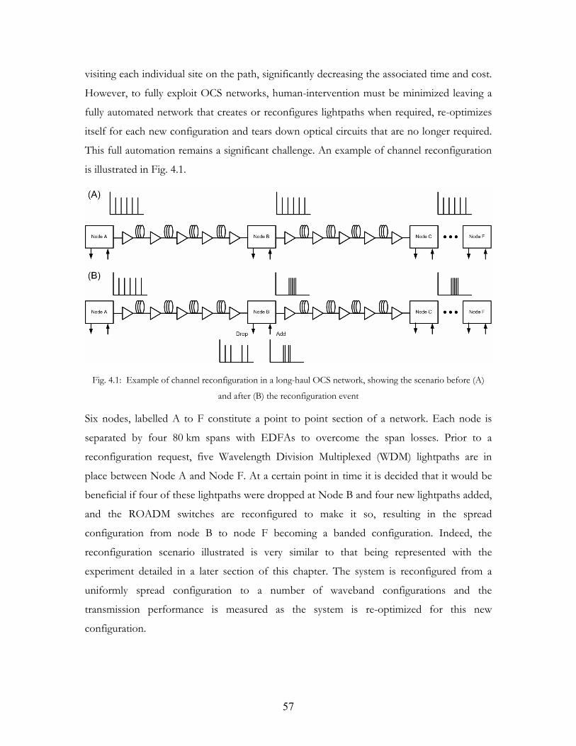
57
visiting each individual site on the path, significantly decreasing the associated time and cost.
However, to fully exploit OCS networks, human-intervention must be minimized leaving a
fully automated network that creates or reconfigures lightpaths when required, re-optimizes
itself for each new configuration and tears down optical circuits that are no longer required.
This full automation remains a significant challenge. An example of channel reconfiguration
is illustrated in Fig. 4.1.
Fig. 4.1: Example of channel reconfiguration in a long-haul OCS network, showing the scenario before (A)
and after (B) the reconfiguration event
Six nodes, labelled A to F constitute a point to point section of a network. Each node is
separated by four 80 km spans with EDFAs to overcome the span losses. Prior to a
reconfiguration request, five Wavelength Division Multiplexed (WDM) lightpaths are in
place between Node A and Node F. At a certain point in time it is decided that it would be
beneficial if four of these lightpaths were dropped at Node B and four new lightpaths added,
and the ROADM switches are reconfigured to make it so, resulting in the spread
configuration from node B to node F becoming a banded configuration. Indeed, the
reconfiguration scenario illustrated is very similar to that being represented with the
experiment detailed in a later section of this chapter. The system is reconfigured from a
uniformly spread configuration to a number of waveband configurations and the
transmission performance is measured as the system is re-optimized for this new
configuration.
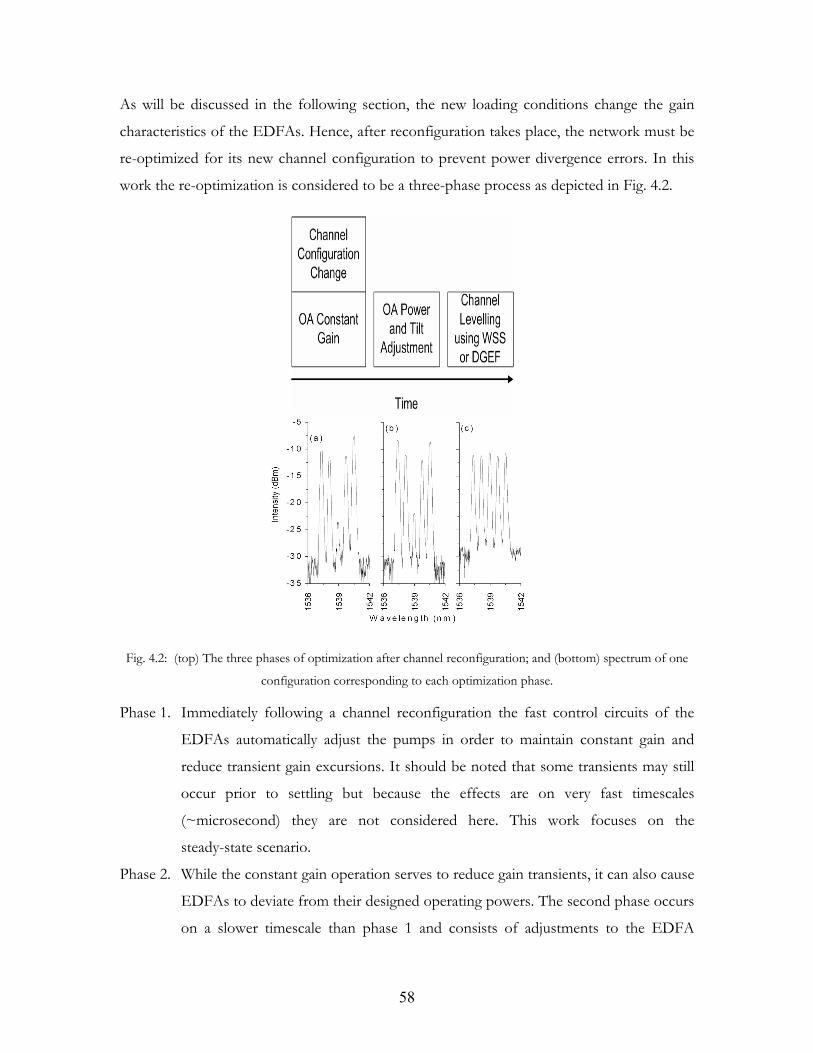
58
As will be discussed in the following section, the new loading conditions change the gain
characteristics of the EDFAs. Hence, after reconfiguration takes place, the network must be
re-optimized for its new channel configuration to prevent power divergence errors. In this
work the re-optimization is considered to be a three-phase process as depicted in Fig. 4.2.
Fig. 4.2: (top) The three phases of optimization after channel reconfiguration; and (bottom) spectrum of one
configuration corresponding to each optimization phase.
Phase 1. Immediately following a channel reconfiguration the fast control circuits of the
EDFAs automatically adjust the pumps in order to maintain constant gain and
reduce transient gain excursions. It should be noted that some transients may still
occur prior to settling but because the effects are on very fast timescales
(~microsecond) they are not considered here. This work focuses on the
steady-state scenario.
Phase 2. While the constant gain operation serves to reduce gain transients, it can also cause
EDFAs to deviate from their designed operating powers. The second phase occurs
on a slower timescale than phase 1 and consists of adjustments to the EDFA
59
pumps and Variable Optical Attenuators (VOAs) in order to return to the
designed operating output power and spectral tilt.
Phase 3. The third phase is a fine tuning phase in which residual gain ripple is levelled out
using per channel VOAs or a dynamic Gain Equalization Filter (GEF).
The spectra in Fig. 4.2 show the effect of these optimization stages.
4.2 EDFAs in long haul networks To assist with the description of EDFA gain dynamics and their effect on a long haul
system, Fig. 4.3 depicts a schematic of a typical EDFA which may be used in a long haul
network.
Fig. 4.3: Typical two-stage EDFA schematic incorporating two erbium doped fiber (EDF) gain stages, and an
ASE Filter, external dispersion compensation module (DCM), gain equalization filter (GEF) and variable
optical attenuator (VOA).
EDFAs have evolved from single gain blocks to multi-stage amplification sub-systems with
many elements providing added functionality between the stages such as Dispersion
Compensation Modules (DCMs), VOAs for gain tilt adjustment, filters to remove Amplified
Spontaneous Emission (ASE) added in the first stage, and GEFs to flatten the gain profile of
the EDFA. The mid-stage placement of these components reduces the Optical Signal to
Noise Ratio (OSNR) impact that they would have if placed outside the amplifier. In
addition, because they are passive components, they do not impact the noise figure. In
general the input stage is operated with high gain and the output stage is operated in
saturation with high output power. The overall noise figure is decided mainly by the input
stage as can be seen from the following equation [2]:
1
21 GL
NFNFNFMID
+= (4.1)
60
where NF1 and NF2 are the noise figure of the first and second stage, respectively, LMID is
the mid-stage loss and G1 is the gain of the first stage.
4.2.1 EDFA Noise and OSNR The OSNR determines the reach of an optically amplified long haul system. A regularly used
performance metric for long haul systems is the ‘required OSNR’; a measurement of the
minimum OSNR at which a certain Bit Error Rate (BER) can be achieved. In this work a
BER of 1x10⁻³ was used for required OSNR measurements as this can be corrected to an
error rate of 1x10-12 or better using Forward Error Correction (FEC). In WDM systems, the
best case OSNR is set by the amount of ASE generated by the EDFAs in the path. OSNR
penalties can then be introduced by many factors, including but not limited to, linear
crosstalk, polarization effects, non-linear crosstalk, and dispersion. These impairments,
which must be factored into the OSNR budget during system design, will be the topic of
Section 4.3. In a reconfigurable mesh network this task becomes much more arduous given
that signals can be routed to a particular destination via a number of paths.
ASE is the most severe limiter of reach in long haul systems. Its generation is an inevitable
consequence of optical amplification that results in signal-spontaneous beat noise at the
receiver and it represents the fundamental noise limit of the system. Each EDFA contributes
ASE according to Equation 3.1, and the contributions along a chain of EDFAs add
cumulatively.
)1(2 −⋅∆⋅= GnvhvP spASE (4.2)
where PASE is the ASE power in an optical bandwidth ∆ν, h is Planck’s constant, ν is the
optical frequency, nsp is the spontaneous emission factor and G is the gain of the EDFA.
The OSNR is defined as the ratio of optical signal channel power to the power of the ASE
in a given bandwidth (usually 0.1nm). When designing the system, the target OSNR at the
receiver must be sufficiently high, so as to give the required system performance, and must
include sufficient margin to allow for any impairments which may be encountered.
For a chain of EDFAs the OSNR at the end of the chain is given by the following equation:
)(log1058)( 10 ampspanout NNFLPdBOSNR −−−+= (4.3)
61
where Pout is the channel output power of the EDFA, Lspan is the loss through each span, NF
is the noise figure of the EDFAs and Namp is the number of amplifiers. While this equation is
rarely accurate in practical networks because neither fiber spans nor EDFAs are likely to be
uniform across the entire network, it gives a useful indication of some of the constraints due
to amplifier noise. For circulating loops that by their very nature exhibit increased uniformity
its accuracy improves and it is used later in this chapter to verify that the shape of the
measured OSNR as a function of distance in the circulating loop agrees with expectations
for a straight line system.
A 3dB increase in OSNR allows the reach to be doubled, and a 1dB increase allows a reach
increase of approximately 25%. The equation shows us that a 1dB increase in final OSNR
can be obtained by:
(a) increasing the output power by 1dB,
(b) reducing the span loss by 1dB, or by
(c) reducing the noise figure by 1dB.
Due to the logarithm in the final term of the equation, the number of amplifiers is a less
important factor than these other terms. Increasing the output power is only viable to a
certain extent due to the onset of nonlinearities at high optical powers. The noise figure in a
high gain EDFA is limited to values above 3dB and typical values are 5dB with little scope
for reduction. The other option is to reduce the span loss and while this is useful and
common for underwater systems, limited availability of amplifier sites reduce it’s viability for
terrestrial applications. Distributed Raman amplification has improved noise characteristics
over lumped amplification used in EDFAs and is seen as a promising technology to increase
transmission reach.
4.2.2 EDFA gain flatness and the effect on OSNR Amplifier gain flatness is a critical parameter for WDM networks. Through a chain of
EDFAs, the non-uniformity of the gain spectrum accumulates and can lead to a large power
divergence between channels in a network. Channels which experience low gain can suffer
from OSNR related penalties whilst channels in a high gain region of the spectrum can reach
powers above the non-linear threshold which also causes performance degradation. The
GEFs used in EDFAs are optimized to flatten the spectrum of a fully loaded EDFA [2].
62
Under varied loading conditions that may be caused by reconfiguration or failure, the gain
uniformity decreases, the GEF becomes less effective, and the gain ripple increases. The
entire gain spectrum of an EDFA gets tilted when the average inversion level of the erbium
is changed. Gain tilt is another effect with similar ramifications to gain ripple, including
power divergence and OSNR penalties. As shown in Fig. 4.3 a VOA is often added to the
midstage of the EDFA and this can be used to vary the gain tilt by controlling the average
inversion level. Yet another effect, Spectral Hole Burning (SHB) is the result of a small
amount of inhomogeneity in the gain spectrum and it causes loading dependent gain
reduction around channels or groups of channels [3]. The depth of the gain reduction hole
depends on how saturated the gain of the EDFA is, and is also strongly wavelength
dependent, with the effect at 1532nm being four times stronger than at 1551nm [4, 5]. The
performance penalties caused by each of these gain effects will remain in place until the
system is optimized for the new loading configuration. As mentioned, re-optimization
involves the adjustment of the amplifier powers and variation of the GEFs.
4.2.3 Transient gain dynamics EDFAs in long haul networks are generally operated in saturation in order to reduce the
amount of ASE generated, and the available gain is shared by all of the channels. If a channel
or group of channels is added or dropped accidentally due to failure somewhere in the
network, or intentionally due to channel reconfiguration, a transient gain excursion occurs
due to the cross saturation effect [6]. The modelling [7], control [8] and effects [9, 10] of
these gain transients have been studied by many groups. In early work, the time constant of
gain recovery for a single stage EDFA was measured to be between 110 µs and 340µs [11].
Later reports stated that in a two stage EDFA the time constant is in the tens of
microseconds range due to the higher saturation factors required in the today’s high power
EDFAs [12]. When a smaller percentage of channels are dropped, the time constant
decreases further and in chains of EDFAs the effect is faster still [13]. If half of the channels
are dropped, each EDFAs output power initially drops by 3dB at time t=0. In order to
conserve the saturated output power, the gain in all of the amplifiers then begins to grow.
This means that at the same time as the output power of the first EDFA is growing, the gain
of the second EDFA is also growing and so on down the chain of EDFAs. This cascading
effect means that the transient time gets faster and faster as the network size, or number of
63
amplifiers in a chain increases [14]. Transient effects can cause unacceptable errors in the
system due to nonlinearities associated with high power spikes, and power dips at the
receiver; they must therefore be minimized using dynamic gain control with a faster response
time than the time constant of the transient. A number of channel protection schemes have
been devised in order to reduce the effects of transients. Prior to these methods, EDFAs
were operated in a constant output power mode such that a power change at the input to the
EDFA did not result in a power change at the output. In contrast, these methods attempt to
maintain constant gain, such that a proportional reduction in output power accompanies a
reduction in input power. The techniques include:
(i) Pump control [15] operating on timescales of microseconds can be
employed to limit the power transients on surviving channels. In [16] the
authors reduce the power excursions from greater than 6dB to less than
0.5dB using this method. The control circuit acts within 8µs.
(ii) Optical control [17,18] achieves gain stabilization by feeding a portion of
the output light back into the input of the EDFA.
(iii) Link control makes use of a control channel that is used for an entire
link. It is coupled into the system at a node and decoupled out at the next
node. An optical tap in the link monitors the power and this in
conjunction with a feedback control circuit adjusts the power of the
control channel in order to maintain constant input power for the first
amplifier and hence constant power for the entire link.
4.2.4 Steady state gain dynamics After the transient effects have settled down the EDFAs return to a steady state but there
are also dynamic effects associated with the steady state gain due to variations in channel
loading. Steady state gain dynamics of EDFAs in reconfigurable networks have received less
attention than their transient counterparts, however recently a number of studies have
illustrated the importance of gaining an in-depth understanding of the effects and the
limitations that they can place on the system. Early work used constant-power controlled
EDFAs and noted instabilities associated with particular network configurations and control
strategies [19]. The use of Constant Gain Control (CGC) was found to reduce the impact.
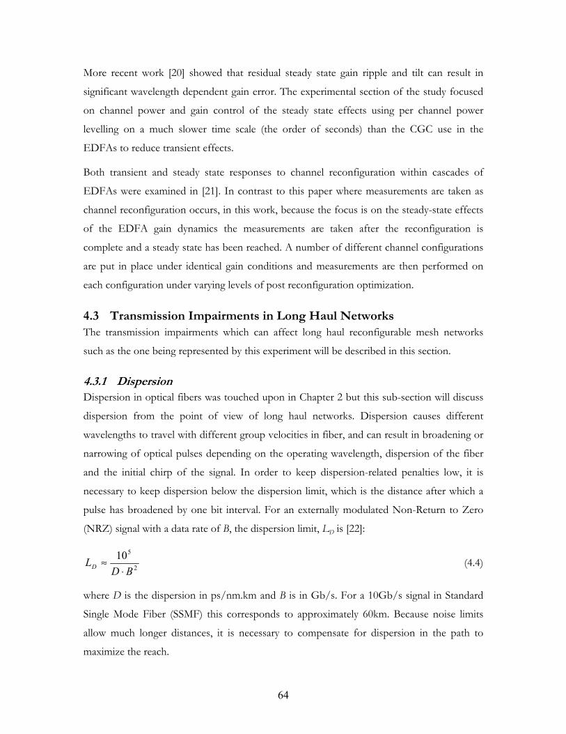
64
More recent work [20] showed that residual steady state gain ripple and tilt can result in
significant wavelength dependent gain error. The experimental section of the study focused
on channel power and gain control of the steady state effects using per channel power
levelling on a much slower time scale (the order of seconds) than the CGC use in the
EDFAs to reduce transient effects.
Both transient and steady state responses to channel reconfiguration within cascades of
EDFAs were examined in [21]. In contrast to this paper where measurements are taken as
channel reconfiguration occurs, in this work, because the focus is on the steady-state effects
of the EDFA gain dynamics the measurements are taken after the reconfiguration is
complete and a steady state has been reached. A number of different channel configurations
are put in place under identical gain conditions and measurements are then performed on
each configuration under varying levels of post reconfiguration optimization.
4.3 Transmission Impairments in Long Haul Networks The transmission impairments which can affect long haul reconfigurable mesh networks
such as the one being represented by this experiment will be described in this section.
4.3.1 Dispersion Dispersion in optical fibers was touched upon in Chapter 2 but this sub-section will discuss
dispersion from the point of view of long haul networks. Dispersion causes different
wavelengths to travel with different group velocities in fiber, and can result in broadening or
narrowing of optical pulses depending on the operating wavelength, dispersion of the fiber
and the initial chirp of the signal. In order to keep dispersion-related penalties low, it is
necessary to keep dispersion below the dispersion limit, which is the distance after which a
pulse has broadened by one bit interval. For an externally modulated Non-Return to Zero
(NRZ) signal with a data rate of B, the dispersion limit, LD is [22]:
2
510BD
LD ⋅≈ (4.4)
where D is the dispersion in ps/nm.km and B is in Gb/s. For a 10Gb/s signal in Standard
Single Mode Fiber (SSMF) this corresponds to approximately 60km. Because noise limits
allow much longer distances, it is necessary to compensate for dispersion in the path to
maximize the reach.
65
If nonlinearities played no part then compensating for dispersion would simply require the
use of Dispersion Shifted Fiber (DSF) for the entire path, with the required Dispersion
Compensation Fiber (DCF) for each channel placed at the end to ensure that wavelengths
that are not at the zero dispersion point do not exceed the dispersion limit. In long haul
systems however, it is generally desirable to launch into each span of fiber with as much
power as possible meaning that nonlinearities do come into effect. In order to maximize
performance it is necessary to manage the dispersion, not only at the end of the system but
throughout the entire path. The placement and amount of dispersion compensation forms
the “dispersion map” and its design is critical to minimize penalties from nonlinearities and
hence allow maximum launch power and OSNR [23]. Keeping the accumulated dispersion
sufficiently low at all points in the system prevents nonlinear phase modulations from being
converted into amplitude modulations. On the other hand, if local dispersion is too low,
strong phase matching between signals and long distances over which wavelengths overlap,
can cause certain non-linear effects such as Four Wave Mixing (FWM) to be severe.
Much of the fiber installed today is SSMF which has a dispersion of 0ps/nm.km at 1300nm
and approximately 17ps/nm.km at 1550nm. This large dispersion at the EDFA operating
wavelength led to the development of DSF which has its dispersion zero at 1550nm. As was
mentioned previously however, a small amount of dispersion is beneficial because it spreads
pulses out, thereby reducing the peak power and reducing the FWM intermodulations which
are most deleterious at high power peaks. Non-Zero Dispersion Shifted Fiber (NZDSF), is
the compromise between SSMF and DSF. With a dispersion of 3-8ps/nm.km at 1550nm, it
is large enough to reduce FWM but small enough to keep total accumulated dispersion low.
Many transmission fiber designs exhibit a large wavelength dependence (dispersion slope),
while the slope of DCF is often much flatter. Hence the best dispersion map for the central
channel in the band is non-ideal for wavelength channels above or below this wavelength
and dispersion “walk-off” can occur. This walk-off is illustrated in Fig. 4.4 which shows the
dispersion map for the central channel as a solid line and a higher wavelength channel as a
dotted line. In this plot the dispersion for the central channel and higher wavelength channel
are 17 and 20ps/nm.km respectively. Because the DCF (placed every 80km) compensates
each channel for 17ps/nm.km the higher wavelength channels experiences the walk-off.
More recent fiber designs have lowered the wavelength dependence (dispersion slope)
making it easier to keep the entire band of channels within the dispersion limit. Walk-off can
66
also occur due to the fact that dispersion compensation modules (DCMs) are generally
available in discrete values and are generally not matched exactly to the spans.
Fig. 4.4: Dispersion map for two channels. The solid line represents the zero-dispersion wavelength and the
dotted line represents a higher wavelength. Mismatch between the dispersion slope of the span fiber and the
compensating fiber leads to the walk off shown.
Optimized dispersion map design is critical for long haul networks. The use of dispersion
pre-compensation and post compensation has been shown to reduce the effects of
nonlinearities and improve performance [24]. In mesh networks channels that have travelled
various distances and over different fiber plant can be present on the same fiber, making
dispersion map design an even greater challenge. The work detailed in this chapter makes
use of two dispersion maps which will be described in the experimental section.
4.3.2 Nonlinearities Nonlinear effects occur in fiber when the response of the fiber is a nonlinear function of the
amplitude of the electromagnetic field applied and they can be categorized into two distinct
types:
1) Stimulated scattering effects (including Raman and Brillouin scattering) and,
2) Effects arising from the Kerr effect (including Cross-Phase Modulation (XPM), Self-
Phase Modulation (SPM) and FWM).
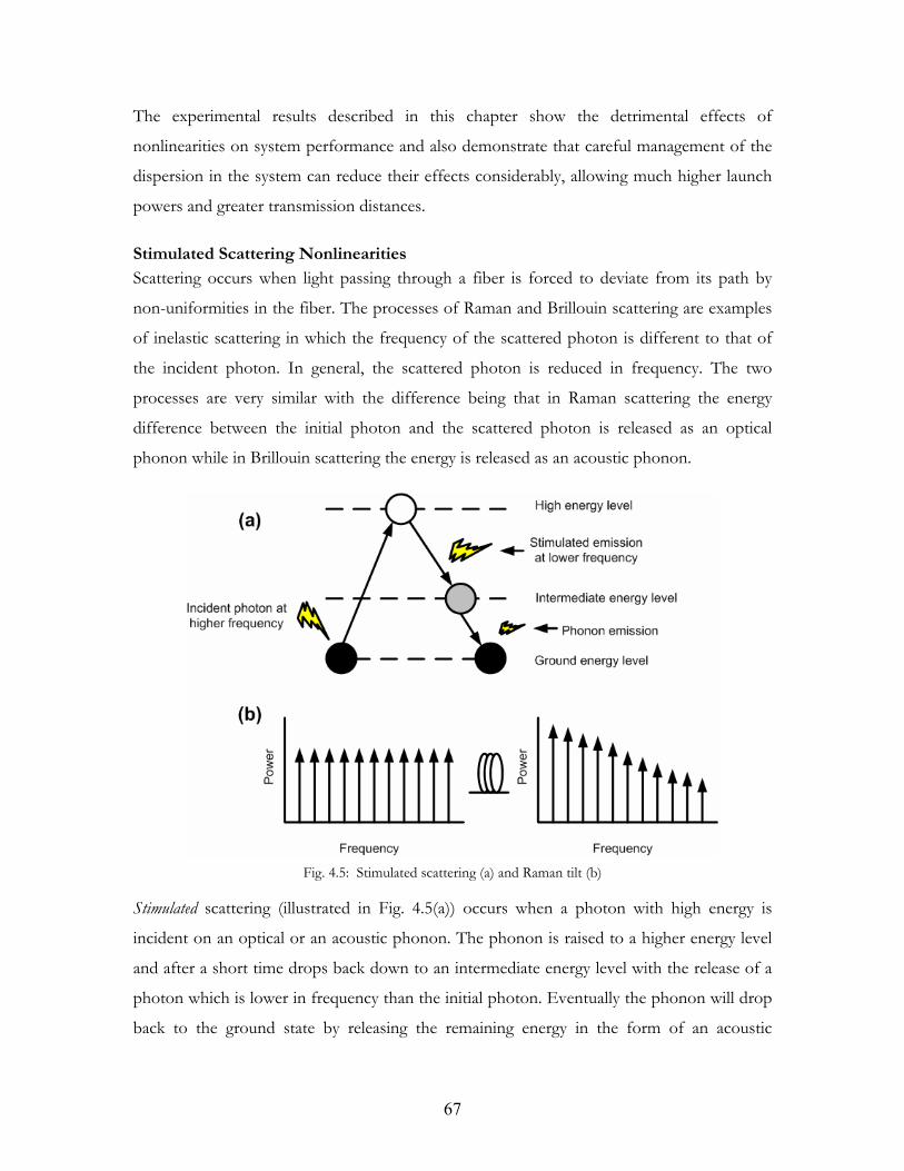
67
The experimental results described in this chapter show the detrimental effects of
nonlinearities on system performance and also demonstrate that careful management of the
dispersion in the system can reduce their effects considerably, allowing much higher launch
powers and greater transmission distances.
Stimulated Scattering Nonlinearities Scattering occurs when light passing through a fiber is forced to deviate from its path by
non-uniformities in the fiber. The processes of Raman and Brillouin scattering are examples
of inelastic scattering in which the frequency of the scattered photon is different to that of
the incident photon. In general, the scattered photon is reduced in frequency. The two
processes are very similar with the difference being that in Raman scattering the energy
difference between the initial photon and the scattered photon is released as an optical
phonon while in Brillouin scattering the energy is released as an acoustic phonon.
Fig. 4.5: Stimulated scattering (a) and Raman tilt (b)
Stimulated scattering (illustrated in Fig. 4.5(a)) occurs when a photon with high energy is
incident on an optical or an acoustic phonon. The phonon is raised to a higher energy level
and after a short time drops back down to an intermediate energy level with the release of a
photon which is lower in frequency than the initial photon. Eventually the phonon will drop
back to the ground state by releasing the remaining energy in the form of an acoustic
68
phonon for Stimulated Brillouin Scattering (SBS) or in the form of an optical phonon for
Stimulated Raman Scattering (SRS).
The main differences in the two effects, caused by the difference in dispersion for optical
and acoustic phonons are as follows:
(iv) SBS only occurs in the backward direction while SRS can occur in both
directions
(v) The frequency shift is approximately 10GHz for SBS but 13THz for
SRS.
(vi) The Brillouin gain spectrum has a very narrow bandwidth (<100MHz)
whereas the Raman gain spectrum is of the order of 30THz.
The SBS process results in signal loss in the direction of propagation and distortion in the
backwards direction caused by reflections. SBS has the lowest threshold of all the optical
nonlinearities [25] and can impact a system at optical channel powers as low as 1mW.
However, this is for very narrow light sources and the effects are reduced by using a light
source of relatively broad spectral width or through the use of phase shift keying or other
modulation schemes.
The use of Raman scattering for amplification was described in Chapter 2. However, Raman
scattering can also occur between signal channels, when lower wavelength channels pump
(transfer energy to) higher wavelength channels. This leads to wavelength dependent loss
and spectral tilt in a WDM system as shown in Fig. 4.5(b). The effect grows in each fiber
span so in long haul systems consisting of many spans it is often compensated for, either
through the use of per-channel VOAs in the nodes, or by tilting the gain spectrum of the
EDFAs using a VOA in the mid-stage section of a two-stage EDFA for example.
Kerr Effect Nonlinearities The refractive index, n, of silica optical fibers varies with optical power, P, according to the
following equation:
effAPnnn 20 += (4.5)
69
where n0 is the refractive index at low powers, Aeff is the effective area of the optical mode in
the fiber and n2 is the nonlinear index co-efficient which is typically around 2.6 x 10⁻²⁰ m2/W
in SSMF [26]. The intensity dependence of the refractive index causes an intensity dependent
phase shift in the optical field, known as the Kerr effect. The manifestations of the Kerr
effect will be described below.
Self phase modulation (SPM) SPM occurs when the high peak power of an optical signal increases the refractive index of
the fiber it is travelling through, thereby reducing its group velocity. The result is a change in
the phase of the optical signal and a broadening of its frequency spectrum, which has been
caused by the signal’s own intensity. The envelope of the optical signal in the time domain
does not change due to SPM. However, in any real system dispersion will act on the pulse at
the same time as SPM. In the normal dispersion regime pulses will broaden in time while in
the anomalous dispersion regime pulse compression is caused and the counteracting effects
of SPM. Anomalous broadening can be used to extend the reach of long haul systems which
would otherwise be limited by SPM [27]. The combined broadening by SPM and
compression by anomalous dispersion can also be used to form optical solitons [28]. SPM is
significant when the nonlinear length, LNL (defined as the length of fiber over which
nonlinear effects are significant [28]) is less than the dispersion length, LD (defined as the
length of fiber over which an isolated ‘1’ broadens by √2). In WDM systems with wider
channel spacing SPM is the dominant nonlinear effect however in fiber with high dispersion,
pulses broaden rapidly and hence the high peak powers are quickly reduced, causing a
reduction of the effects of SPM.
Four Wave Mixing (FWM) FWM occurs when closely spaced channels at different frequencies beat together causing
phase modulation of the signals and giving rise to modulation side bands at new frequencies
according to the following equation:
321 ffff FWM −+= (4.6)
The order of the frequencies across the band will then be f1, fFWM, f2, f3. If fFWM lies within the
passband of another channel it will be detected as noise at the receiver. FWM is most
efficient in systems with low channel spacing and low dispersion. It can be avoided by
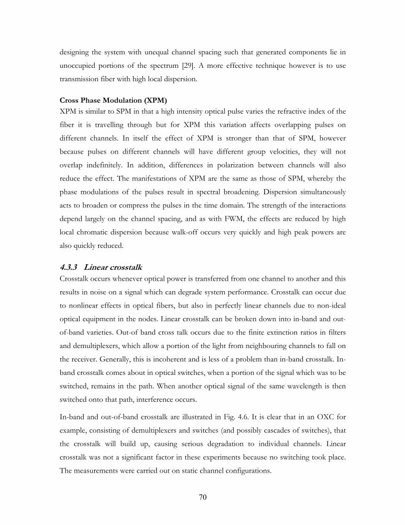
70
designing the system with unequal channel spacing such that generated components lie in
unoccupied portions of the spectrum [29]. A more effective technique however is to use
transmission fiber with high local dispersion.
Cross Phase Modulation (XPM) XPM is similar to SPM in that a high intensity optical pulse varies the refractive index of the
fiber it is travelling through but for XPM this variation affects overlapping pulses on
different channels. In itself the effect of XPM is stronger than that of SPM, however
because pulses on different channels will have different group velocities, they will not
overlap indefinitely. In addition, differences in polarization between channels will also
reduce the effect. The manifestations of XPM are the same as those of SPM, whereby the
phase modulations of the pulses result in spectral broadening. Dispersion simultaneously
acts to broaden or compress the pulses in the time domain. The strength of the interactions
depend largely on the channel spacing, and as with FWM, the effects are reduced by high
local chromatic dispersion because walk-off occurs very quickly and high peak powers are
also quickly reduced.
4.3.3 Linear crosstalk Crosstalk occurs whenever optical power is transferred from one channel to another and this
results in noise on a signal which can degrade system performance. Crosstalk can occur due
to nonlinear effects in optical fibers, but also in perfectly linear channels due to non-ideal
optical equipment in the nodes. Linear crosstalk can be broken down into in-band and out-
of-band varieties. Out-of band cross talk occurs due to the finite extinction ratios in filters
and demultiplexers, which allow a portion of the light from neighbouring channels to fall on
the receiver. Generally, this is incoherent and is less of a problem than in-band crosstalk. In-
band crosstalk comes about in optical switches, when a portion of the signal which was to be
switched, remains in the path. When another optical signal of the same wavelength is then
switched onto that path, interference occurs.
In-band and out-of-band crosstalk are illustrated in Fig. 4.6. It is clear that in an OXC for
example, consisting of demultiplexers and switches (and possibly cascades of switches), that
the crosstalk will build up, causing serious degradation to individual channels. Linear
crosstalk was not a significant factor in these experiments because no switching took place.
The measurements were carried out on static channel configurations.
71
Fig. 4.6: a) Out-of-band crosstalk in a demultiplexer; and b) in-band crosstalk in a switch
4.3.4 Polarization Effects There are three main polarization effects which come into play in long haul systems,
Polarization Dependent Loss (PDL), Polarization Dependent Gain (PDG), and Polarization
Mode Dispersion (PMD). PDG is a weak effect which only comes into play in very long
chains of amplifiers, the likes of which may be used in trans-oceanic systems and will not be
discussed further here. PDL arises from the fact that the components in the system exhibit
different insertion loss depending on the polarization of the light incident on them. In a
practical system PDL affects the OSNR and must be taken into account in the OSNR
budget. It can be kept under control by simply ensuring that low-PDL components are used
in the system. In a circulating loop apparatus PDL plays a larger role because light will pass
through components with the same PDL many times [30]. A polarization scrambler can be
used to reduce this effect and more closely match the PDL performance of a straight-line
system.
PMD comes about because the two orthogonal modes in a fiber have different group delays
due to manufacturing imperfections or stress. The result is that the different polarizations
travel at different speeds through the fibre [31]. PMD is illustrated in Fig. 4.7 with the
Differential Group Delay (DGD) being the group-delay difference between the fast and
slow modes. When the delays approach a significant percentage of the bit period the data
gets distorted and errors occur. Hence, PMD becomes more of a problem at higher bit-rates,
especially above 10Gb/s.
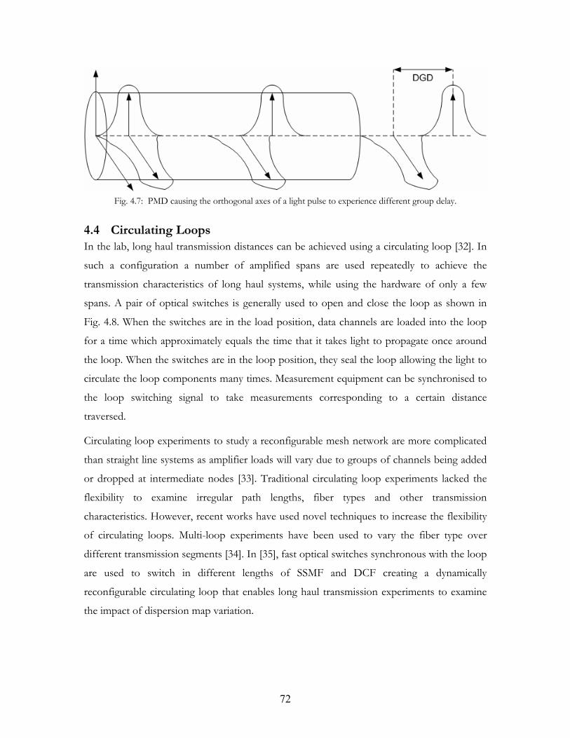
72
Fig. 4.7: PMD causing the orthogonal axes of a light pulse to experience different group delay.
4.4 Circulating Loops In the lab, long haul transmission distances can be achieved using a circulating loop [32]. In
such a configuration a number of amplified spans are used repeatedly to achieve the
transmission characteristics of long haul systems, while using the hardware of only a few
spans. A pair of optical switches is generally used to open and close the loop as shown in
Fig. 4.8. When the switches are in the load position, data channels are loaded into the loop
for a time which approximately equals the time that it takes light to propagate once around
the loop. When the switches are in the loop position, they seal the loop allowing the light to
circulate the loop components many times. Measurement equipment can be synchronised to
the loop switching signal to take measurements corresponding to a certain distance
traversed.
Circulating loop experiments to study a reconfigurable mesh network are more complicated
than straight line systems as amplifier loads will vary due to groups of channels being added
or dropped at intermediate nodes [33]. Traditional circulating loop experiments lacked the
flexibility to examine irregular path lengths, fiber types and other transmission
characteristics. However, recent works have used novel techniques to increase the flexibility
of circulating loops. Multi-loop experiments have been used to vary the fiber type over
different transmission segments [34]. In [35], fast optical switches synchronous with the loop
are used to switch in different lengths of SSMF and DCF creating a dynamically
reconfigurable circulating loop that enables long haul transmission experiments to examine
the impact of dispersion map variation.
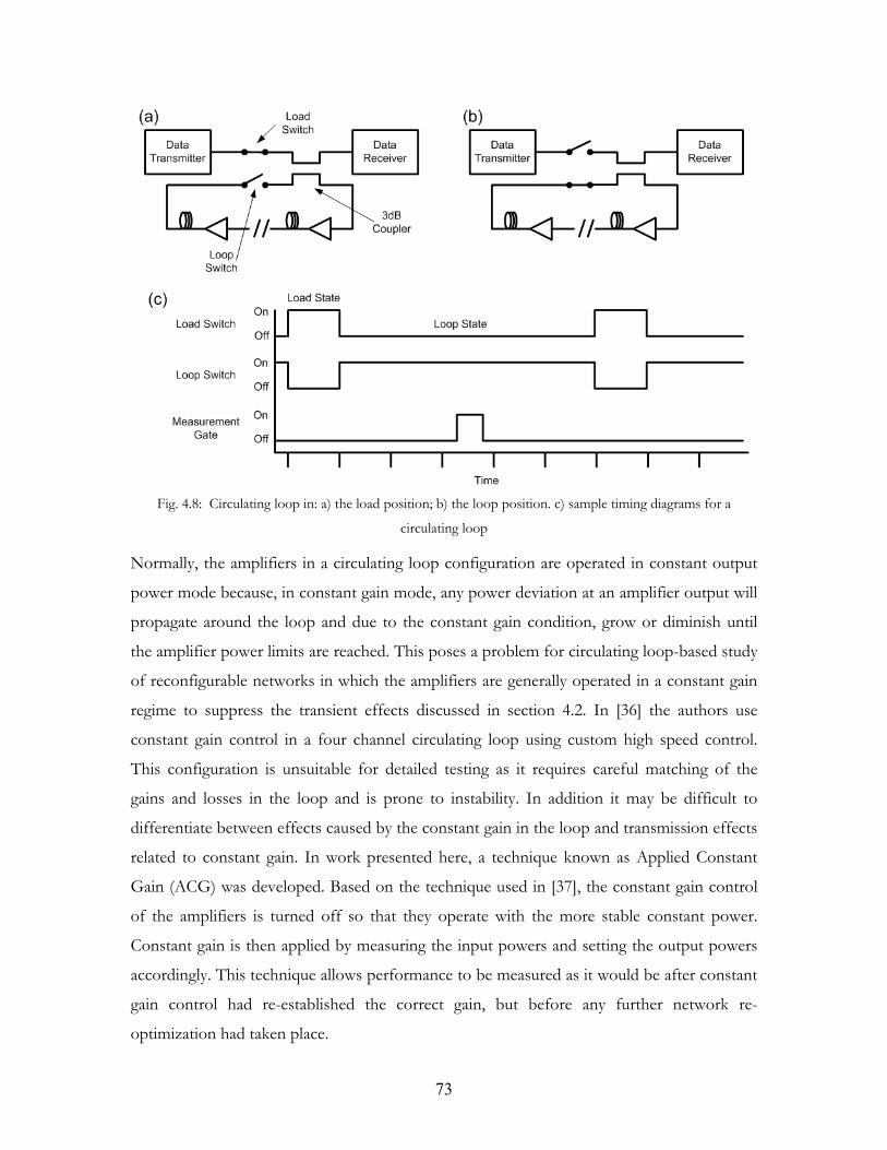
73
Fig. 4.8: Circulating loop in: a) the load position; b) the loop position. c) sample timing diagrams for a
circulating loop
Normally, the amplifiers in a circulating loop configuration are operated in constant output
power mode because, in constant gain mode, any power deviation at an amplifier output will
propagate around the loop and due to the constant gain condition, grow or diminish until
the amplifier power limits are reached. This poses a problem for circulating loop-based study
of reconfigurable networks in which the amplifiers are generally operated in a constant gain
regime to suppress the transient effects discussed in section 4.2. In [36] the authors use
constant gain control in a four channel circulating loop using custom high speed control.
This configuration is unsuitable for detailed testing as it requires careful matching of the
gains and losses in the loop and is prone to instability. In addition it may be difficult to
differentiate between effects caused by the constant gain in the loop and transmission effects
related to constant gain. In work presented here, a technique known as Applied Constant
Gain (ACG) was developed. Based on the technique used in [37], the constant gain control
of the amplifiers is turned off so that they operate with the more stable constant power.
Constant gain is then applied by measuring the input powers and setting the output powers
accordingly. This technique allows performance to be measured as it would be after constant
gain control had re-established the correct gain, but before any further network re-
optimization had taken place.
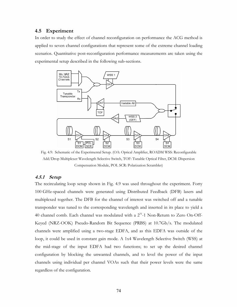
74
4.5 Experiment In order to study the effect of channel reconfiguration on performance the ACG method is
applied to seven channel configurations that represent some of the extreme channel loading
scenarios. Quantitative post-reconfiguration performance measurements are taken using the
experimental setup described in the following sub-sections.
Fig. 4.9: Schematic of the Experimental Setup. (OA: Optical Amplifier, ROADM WSS: Reconfigurable
Add/Drop Multiplexer Wavelength Selective Switch, TOF: Tunable Optical Filter, DCM: Dispersion
Compensation Module, POL SCR: Polarization Scrambler)
4.5.1 Setup The recirculating loop setup shown in Fig. 4.9 was used throughout the experiment. Forty
100 GHz-spaced channels were generated using Distributed Feedback (DFB) lasers and
multiplexed together. The DFB for the channel of interest was switched off and a tunable
transponder was tuned to the corresponding wavelength and inserted in its place to yield a
40 channel comb. Each channel was modulated with a 231-1 Non-Return to Zero On-Off-
Keyed (NRZ-OOK) Pseudo-Random Bit Sequence (PRBS) at 10.7Gb/s. The modulated
channels were amplified using a two-stage EDFA, and as this EDFA was outside of the
loop, it could be used in constant gain mode. A 1x4 Wavelength Selective Switch (WSS) at
the mid-stage of the input EDFA had two functions; to set up the desired channel
configuration by blocking the unwanted channels, and to level the power of the input
channels using individual per channel VOAs such that their power levels were the same
regardless of the configuration.
75
The loop consisted of four amplified spans of Standard Single Mode Fiber (SSMF). The
nominal spans lengths were 80km, 80km, 70km and 90km respectively and the average span
loss was 25.8dB. The amplifiers inside the loop were also two-stage EDFAs. DCMs were
inserted mid-stage in each EDFA and OA3 also had a polarization scrambler in line with its
DCM. An additional two-stage EDFA was placed before the first span to compensate for
component losses between the transmitter and the first span. Each of these EDFAs was
used in constant output power mode. A second WSS used inside the loop represents a node
every five spans in a long haul link. In future work channels can be added or dropped at this
node, but in this work it simply provides channel levelling/gain equalisation and ASE
removal. It was located at the beginning of the loop to represent its position on the add side
of an east/west separable ROADM and was adjusted in order to give a flat and level
spectrum at its own input at all times. This ensured that the loading channels (which were
flattened using WSS1) experienced the same filtration as the looping channels. Due to the
low channel count for the majority of the channel configurations considered, the ASE grew
very rapidly in the loop. In order to improve the OSNR, unused ports on WSS2 were closed
to block any out-of-band ASE.
At the output of the loop the OSNR was varied by attenuating the signal power, while
maintaining constant power on the receiver. A 5nm tunable optical filter in the mid-stage of
the output EDFA was used to reduce the ASE and the signals were demultiplexed using a
100GHz Arrayed Waveguide Grating (AWG) based demultiplexer. The channel of interest
was sent into the receiver of the transponder. The required OSNR for a BER of 1x10⁻³ was
recorded, along with the delivered OSNR at the receiver for each round trip.
4.5.2 Channel Configurations Configuration 1 consisted of forty 100GHz spaced C-band channels. Configuration 2
consisted of five of these channels spread across the C-band. The wavelengths of these
channels were 1532.68nm, 1538.98nm, 1546.12nm, 1553.33nm and 1559.79nm.
Configurations 3 – 7 consisted of a band of five channels with one of the channels from
Configuration 2 as the centre channel together with its two nearest higher frequency
neighbours and its two nearest lower frequency neighbours. Three of the configurations are
shown in Fig. 4.10 after one round trip. These configurations represent extreme cases of
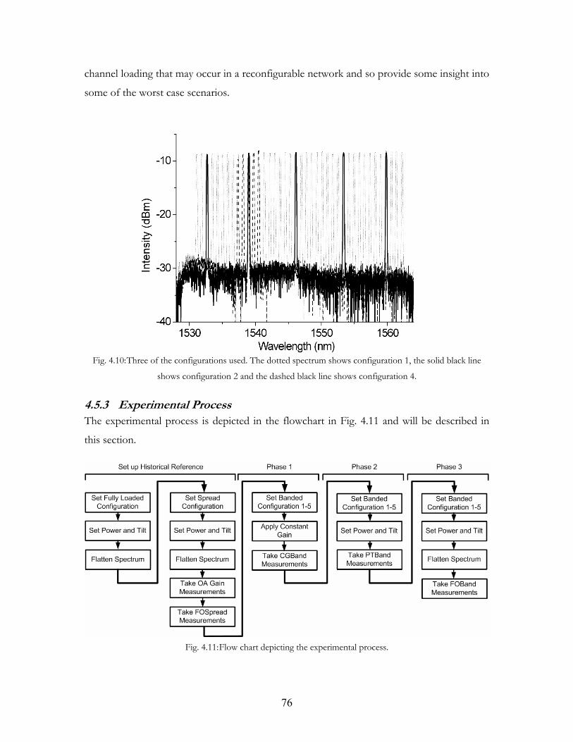
76
channel loading that may occur in a reconfigurable network and so provide some insight into
some of the worst case scenarios.
Fig. 4.10: Three of the configurations used. The dotted spectrum shows configuration 1, the solid black line
shows configuration 2 and the dashed black line shows configuration 4.
4.5.3 Experimental Process The experimental process is depicted in the flowchart in Fig. 4.11 and will be described in
this section.
Fig. 4.11: Flow chart depicting the experimental process.
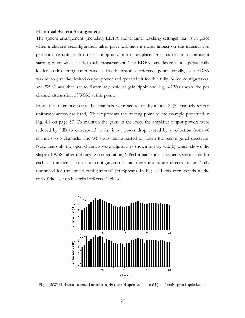
77
Historical System Arrangement The system arrangement (including EDFA and channel levelling settings) that is in place
when a channel reconfiguration takes place will have a major impact on the transmission
performance until such time as re-optimization takes place. For this reason a consistent
starting point was used for each measurement. The EDFAs are designed to operate fully
loaded so this configuration was used as the historical reference point. Initially, each EDFA
was set to give the desired output power and spectral tilt for this fully loaded configuration,
and WSS2 was then set to flatten any residual gain ripple and Fig. 4.12(a) shows the per
channel attenuation of WSS2 at this point.
From this reference point the channels were set to configuration 2 (5 channels spread
uniformly across the band). This represents the starting point of the example presented in
Fig. 4.1 on page 57. To maintain the gains in the loop, the amplifier output powers were
reduced by 9dB to correspond to the input power drop caused by a reduction from 40
channels to 5 channels. The WSS was then adjusted to flatten the reconfigured spectrum.
Note that only the open channels were adjusted as shown in Fig. 4.12(b) which shows the
shape of WSS2 after optimizing configuration 2. Performance measurements were taken for
each of the five channels of configuration 2 and these results are referred to as “fully
optimized for the spread configuration” (FOSpread). In Fig. 4.11 this corresponds to the
end of the “set up historical reference” phase.
Fig. 4.12: WSS1 channel attenuations after: a) 40 channel optimization; and b) uniformly spread optimization
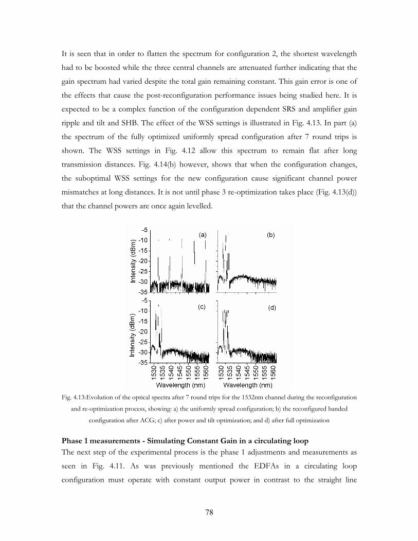
78
It is seen that in order to flatten the spectrum for configuration 2, the shortest wavelength
had to be boosted while the three central channels are attenuated further indicating that the
gain spectrum had varied despite the total gain remaining constant. This gain error is one of
the effects that cause the post-reconfiguration performance issues being studied here. It is
expected to be a complex function of the configuration dependent SRS and amplifier gain
ripple and tilt and SHB. The effect of the WSS settings is illustrated in Fig. 4.13. In part (a)
the spectrum of the fully optimized uniformly spread configuration after 7 round trips is
shown. The WSS settings in Fig. 4.12 allow this spectrum to remain flat after long
transmission distances. Fig. 4.14(b) however, shows that when the configuration changes,
the suboptimal WSS settings for the new configuration cause significant channel power
mismatches at long distances. It is not until phase 3 re-optimization takes place (Fig. 4.13(d))
that the channel powers are once again levelled.
Fig. 4.13: Evolution of the optical spectra after 7 round trips for the 1532nm channel during the reconfiguration
and re-optimization process, showing: a) the uniformly spread configuration; b) the reconfigured banded
configuration after ACG; c) after power and tilt optimization; and d) after full optimization
Phase 1 measurements - Simulating Constant Gain in a circulating loop The next step of the experimental process is the phase 1 adjustments and measurements as
seen in Fig. 4.11. As was previously mentioned the EDFAs in a circulating loop
configuration must operate with constant output power in contrast to the straight line
79
reconfigurable system being represented in which the amplifier’s gains are kept constant. In
order to make meaningful measurements on phase 1 of the optimization cycle it was
necessary to use the ACG technique described previously on the EDFAs used in the loop.
The gain of each loop amplifier was measured prior to reconfiguring away from
Configuration 2. When changing configuration the powers of the loading channels were kept
constant and this, combined with the use of constant gain on the loading amplifier ensured
that the total input power to the loop was kept constant. Inside the loop however, the non-
ideal WSS settings for the new configuration caused the power into the first EDFA to
change. A change in input power to a constant-power-controlled EDFA causes its gain, and
hence its ripple and tilt to change. This effect will propagate through the loop and cause
similar gain changes for all of the other amplifiers in the loop. This situation is undesirable as
it departs from what would occur in a network operating with constant gain. The EDFA
output powers required to revert to the pre-reconfiguration gain can be calculated by
measuring the new input powers to each EDFA. These output powers can then be set while
maintaining the stable constant-power mode in the circulating loop. A change to any EDFA
affects every other EDFA so changes are made iteratively until the gain of each EDFA is
within tolerance. The algorithm achieved a tolerance between desired and achieved gain of
±0.4dB for the total EDFA gain and the EDFA monitor photodiodes were accurate to
±0.1dB. Performance measurements taken at this point are referred to as “constant gain for
the banded configuration” (CGBand). This process is then repeated for configurations 4 – 7.
Phase 2 and Phase 3 Measurements As mentioned in the previous section, channel configuration changes can cause variations in
the wavelength dependent gain even if the EDFA control maintains constant total gain.
Hence, after a reconfiguration it will often be necessary to adjust the amplifiers to re-obtain
the desired channel powers and total spectral tilt. At this point configuration 3 was
reconfigured and the EDFAs output power and tilt were adjusted until target levels were
reached. Fig. 4.13(c) clearly shows the effect of the tilt adjustment however, the channel
power mismatch is still evident despite the mean channel power being correct at this point.
Performance measurements taken after phase 2 re-optimization are referred to as “power
and tilt for the banded configuration” (PTBand). The same process was then repeated for
configurations 4 – 7.

80
Note that up to this point the per-channel levelling shape has not been adjusted for the new
channel configuration and remains as shown in Fig. 4.12(b), optimized for configuration 2.
Clearly this arrangement is non-ideal for configuration 3 (a 5 channel waveband) so phase 3
of the re-optimization process consisted of iteratively adjusting the power and tilt of the
EDFAs, and the shape of the WSS in order to get a flat spectrum with all channels at the
desired mean channel power as shown in Fig. 4.14(d). Once this was achieved,
measurements were taken and these are referred to as “fully optimized for the banded
configuration” (FOBand). Again, similar measurements were taken for configurations 4 – 7
and this completed the experimental process.
To summarise, the configuration is changed from five uniformly spread channels to five
banded channels as shown in Fig. 4.14 (a & b) for the 1532nm channel. Performance
measurements are taken at both of these points as well as at two further optimization stages
Fig. 4.13 (c & d). The same measurements are taken for each of the five initial channels,
yielding a total of 20 sets of measurements. The naming conventions used in figures and text
to describe these are as follows:
(i) Fully Optimized (phase 3 measurements) with five channel spread across the
band are referred to as FOxxxxSpread.
(ii) Applied Constant Gain (phase 1 measurements) with 5 channels banded together
are referred to as CGxxxxBand.
(iii) Power and Tilt (phase 2 measurements) with 5 channels banded together are
referred to as PTxxxxBand.
(iv) Fully Optimized (phase 3 measurements) with five channels banded together are
referred to as FOxxxxBand.
For example CG1538Band refers to Constant Gain (phase 1 measurements) of the 1538
channel in the banded configuration and FO1559Spread refers to the Fully Optimized
(phase 3 measurements) of the 1559 channel when it is part of the configuration with 5
channels spread across the band.
4.5.4 Channel Launch Powers and Dispersion Maps The process outlined above was performed using four different channel launch powers
(0dBm, 2dBm, 4dBm and 6dBm). ‘Return-to-zero’ dispersion maps (where the DCMs and
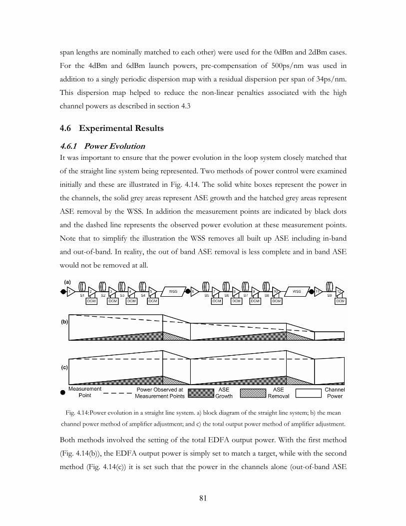
81
span lengths are nominally matched to each other) were used for the 0dBm and 2dBm cases.
For the 4dBm and 6dBm launch powers, pre-compensation of 500ps/nm was used in
addition to a singly periodic dispersion map with a residual dispersion per span of 34ps/nm.
This dispersion map helped to reduce the non-linear penalties associated with the high
channel powers as described in section 4.3
4.6 Experimental Results
4.6.1 Power Evolution It was important to ensure that the power evolution in the loop system closely matched that
of the straight line system being represented. Two methods of power control were examined
initially and these are illustrated in Fig. 4.14. The solid white boxes represent the power in
the channels, the solid grey areas represent ASE growth and the hatched grey areas represent
ASE removal by the WSS. In addition the measurement points are indicated by black dots
and the dashed line represents the observed power evolution at these measurement points.
Note that to simplify the illustration the WSS removes all built up ASE including in-band
and out-of-band. In reality, the out of band ASE removal is less complete and in band ASE
would not be removed at all.
Fig. 4.14: Power evolution in a straight line system. a) block diagram of the straight line system; b) the mean
channel power method of amplifier adjustment; and c) the total output power method of amplifier adjustment.
Both methods involved the setting of the total EDFA output power. With the first method
(Fig. 4.14(b)), the EDFA output power is simply set to match a target, while with the second
method (Fig. 4.14(c)) it is set such that the power in the channels alone (out-of-band ASE
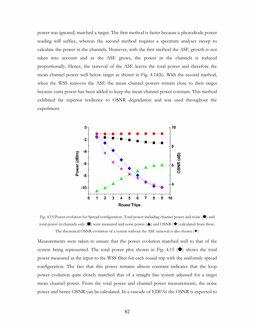
82
power was ignored) matched a target. The first method is faster because a photodiode power
reading will suffice, whereas the second method requires a spectrum analyser sweep to
calculate the power in the channels. However, with the first method the ASE growth is not
taken into account and as the ASE grows, the power in the channels is reduced
proportionally. Hence, the removal of the ASE leaves the total power and therefore the
mean channel power well below target as shown in Fig. 4.14(b). With the second method,
when the WSS removes the ASE the mean channel powers remain close to their target
because extra power has been added to keep the mean channel power constant. This method
exhibited far superior resilience to OSNR degradation and was used throughout the
experiment.
Fig. 4.15: Power evolution for Spread configuration. Total power including channel power and noise ( ) and
total power in channels only ( ) were measured and noise power ( ) and OSNR ( ) calculated from these.
The theoretical OSNR evolution of a system without the ASE removal is also shown ( )
Measurements were taken to ensure that the power evolution matched well to that of the
system being represented. The total power plot shown in Fig. 4.15 ( ) shows the total
power measured at the input to the WSS filter for each round trip with the uniformly spread
configuration. The fact that this power remains almost constant indicates that the loop
power evolution quite closely matched that of a straight line system adjusted for a target
mean channel power. From the total power and channel power measurements, the noise
power and hence OSNR can be calculated. In a cascade of EDFAs the OSNR is expected to
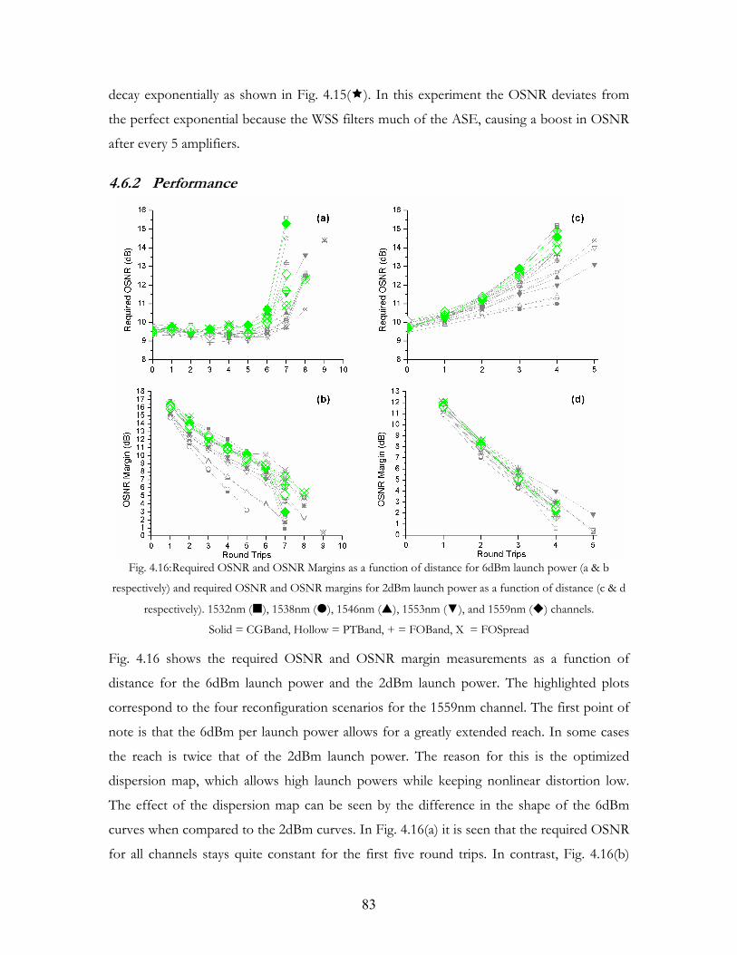
83
decay exponentially as shown in Fig. 4.15( ). In this experiment the OSNR deviates from
the perfect exponential because the WSS filters much of the ASE, causing a boost in OSNR
after every 5 amplifiers.
4.6.2 Performance
Fig. 4.16: Required OSNR and OSNR Margins as a function of distance for 6dBm launch power (a & b
respectively) and required OSNR and OSNR margins for 2dBm launch power as a function of distance (c & d
respectively). 1532nm ( ), 1538nm ( ), 1546nm ( ), 1553nm (▼), and 1559nm ( ) channels.
Solid = CGBand, Hollow = PTBand, + = FOBand, X = FOSpread
Fig. 4.16 shows the required OSNR and OSNR margin measurements as a function of
distance for the 6dBm launch power and the 2dBm launch power. The highlighted plots
correspond to the four reconfiguration scenarios for the 1559nm channel. The first point of
note is that the 6dBm per launch power allows for a greatly extended reach. In some cases
the reach is twice that of the 2dBm launch power. The reason for this is the optimized
dispersion map, which allows high launch powers while keeping nonlinear distortion low.
The effect of the dispersion map can be seen by the difference in the shape of the 6dBm
curves when compared to the 2dBm curves. In Fig. 4.16(a) it is seen that the required OSNR
for all channels stays quite constant for the first five round trips. In contrast, Fig. 4.16(b)
84
shows that despite the lower launch power, the required OSNR increases from the offset
and many of the channels cannot reach five round trips with an acceptable BER even when
fully optimized. Focusing on the highlighted 1559 channel, the OSNR margin plot of Fig.
4.16(b) shows that although the required OSNR remains almost constant for the first five
round trips, the OSNR margin falls quite linearly on account of the degrading delivered
OSNR with each round trip. After this distance the nonlinear effects take hold and a change
in slope is observed. It is seen that the OSNR margin drops by approximately 5dB over the
first 4 round trips. For the 2dBm launch power, the reduction in OSNR margin over the
same distance is approximately 10dB indicating that a reduction in delivered OSNR caused
by the EDFAs and an increase in required OSNR caused by nonlinearities are both affecting
the margin. The change in the slope of the required OSNR curve seen for the 1559nm
channel is not present for the 1538nm channel for example. The reason for this is that the
large WSS attenuation for this channel causes the power for the 1538nm to be too low for
nonlinearities to affect it. The evolution of the channel power for both of these examples
will be seen in Fig. 4.18.
Another interesting point to note from Fig. 4.16(a) is the role played by the reconfiguration
and subsequent re-optimization. Looking at the highlighted 1559nm channel after 7 round
trips it can be seen that the required OSNR varied substantially for each of the scenarios. At
this distance the initial configuration of FO1159Spread exhibits a required OSNR of 10.9dB.
When the configuration changes from spread to banded and constant gain is applied the
required OSNR increases dramatically to 15.3dB due to increased nonlinear effects caused
by XGM between the closely spaced channels, and also the suboptimal WSS setting. Phase 2
optimization involves re-optimizing the power and tilt of the EDFA and results in a 2.7dB
improvement in required OSNR to 12.6dB. When the WSS is adjusted for the new
configuration in phase 3, a further 0.9dB improvement is achieved bringing the required
OSNR to 11.7dB. The 0.8dB difference between the FO1559Spread and FO1559Band is
due to the increased nonlinear penalty associated with the narrower channel spacing.
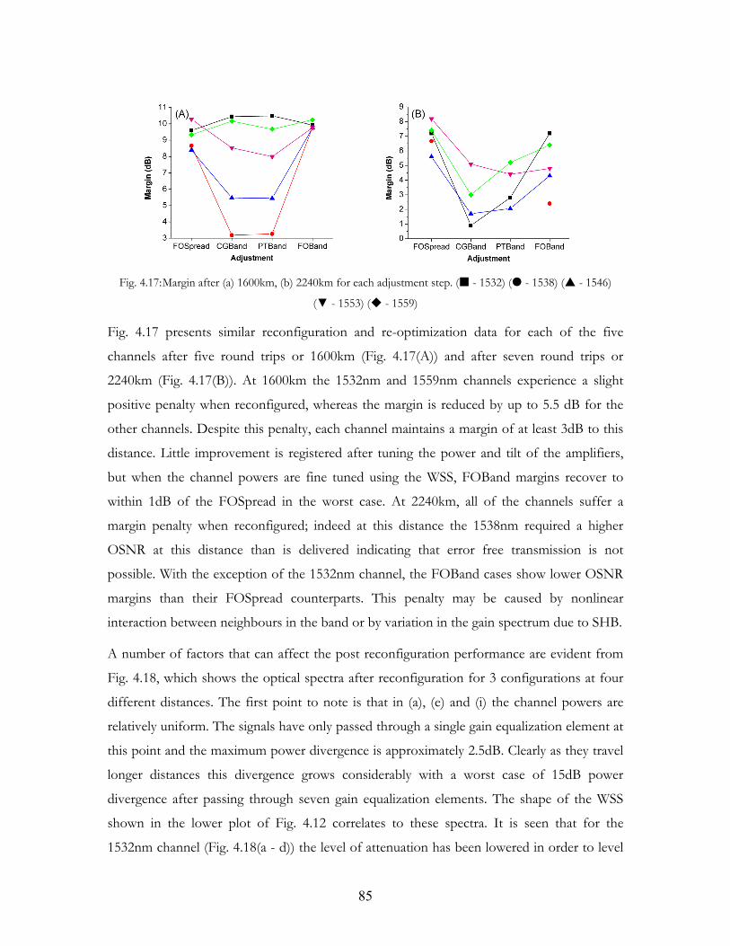
85
Fig. 4.17: Margin after (a) 1600km, (b) 2240km for each adjustment step. ( - 1532) ( - 1538) ( - 1546)
(▼ - 1553) ( - 1559)
Fig. 4.17 presents similar reconfiguration and re-optimization data for each of the five
channels after five round trips or 1600km (Fig. 4.17(A)) and after seven round trips or
2240km (Fig. 4.17(B)). At 1600km the 1532nm and 1559nm channels experience a slight
positive penalty when reconfigured, whereas the margin is reduced by up to 5.5 dB for the
other channels. Despite this penalty, each channel maintains a margin of at least 3dB to this
distance. Little improvement is registered after tuning the power and tilt of the amplifiers,
but when the channel powers are fine tuned using the WSS, FOBand margins recover to
within 1dB of the FOSpread in the worst case. At 2240km, all of the channels suffer a
margin penalty when reconfigured; indeed at this distance the 1538nm required a higher
OSNR at this distance than is delivered indicating that error free transmission is not
possible. With the exception of the 1532nm channel, the FOBand cases show lower OSNR
margins than their FOSpread counterparts. This penalty may be caused by nonlinear
interaction between neighbours in the band or by variation in the gain spectrum due to SHB.
A number of factors that can affect the post reconfiguration performance are evident from
Fig. 4.18, which shows the optical spectra after reconfiguration for 3 configurations at four
different distances. The first point to note is that in (a), (e) and (i) the channel powers are
relatively uniform. The signals have only passed through a single gain equalization element at
this point and the maximum power divergence is approximately 2.5dB. Clearly as they travel
longer distances this divergence grows considerably with a worst case of 15dB power
divergence after passing through seven gain equalization elements. The shape of the WSS
shown in the lower plot of Fig. 4.12 correlates to these spectra. It is seen that for the
1532nm channel (Fig. 4.18(a - d)) the level of attenuation has been lowered in order to level
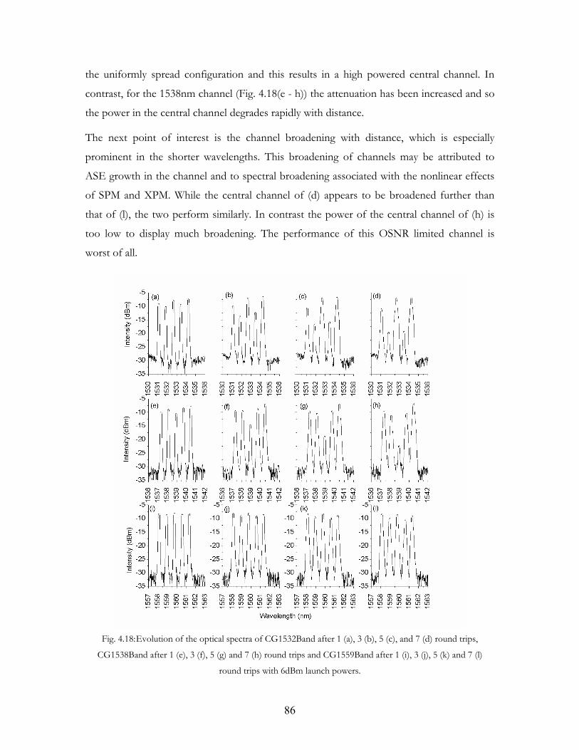
86
the uniformly spread configuration and this results in a high powered central channel. In
contrast, for the 1538nm channel (Fig. 4.18(e - h)) the attenuation has been increased and so
the power in the central channel degrades rapidly with distance.
The next point of interest is the channel broadening with distance, which is especially
prominent in the shorter wavelengths. This broadening of channels may be attributed to
ASE growth in the channel and to spectral broadening associated with the nonlinear effects
of SPM and XPM. While the central channel of (d) appears to be broadened further than
that of (l), the two perform similarly. In contrast the power of the central channel of (h) is
too low to display much broadening. The performance of this OSNR limited channel is
worst of all.
Fig. 4.18: Evolution of the optical spectra of CG1532Band after 1 (a), 3 (b), 5 (c), and 7 (d) round trips,
CG1538Band after 1 (e), 3 (f), 5 (g) and 7 (h) round trips and CG1559Band after 1 (i), 3 (j), 5 (k) and 7 (l)
round trips with 6dBm launch powers.
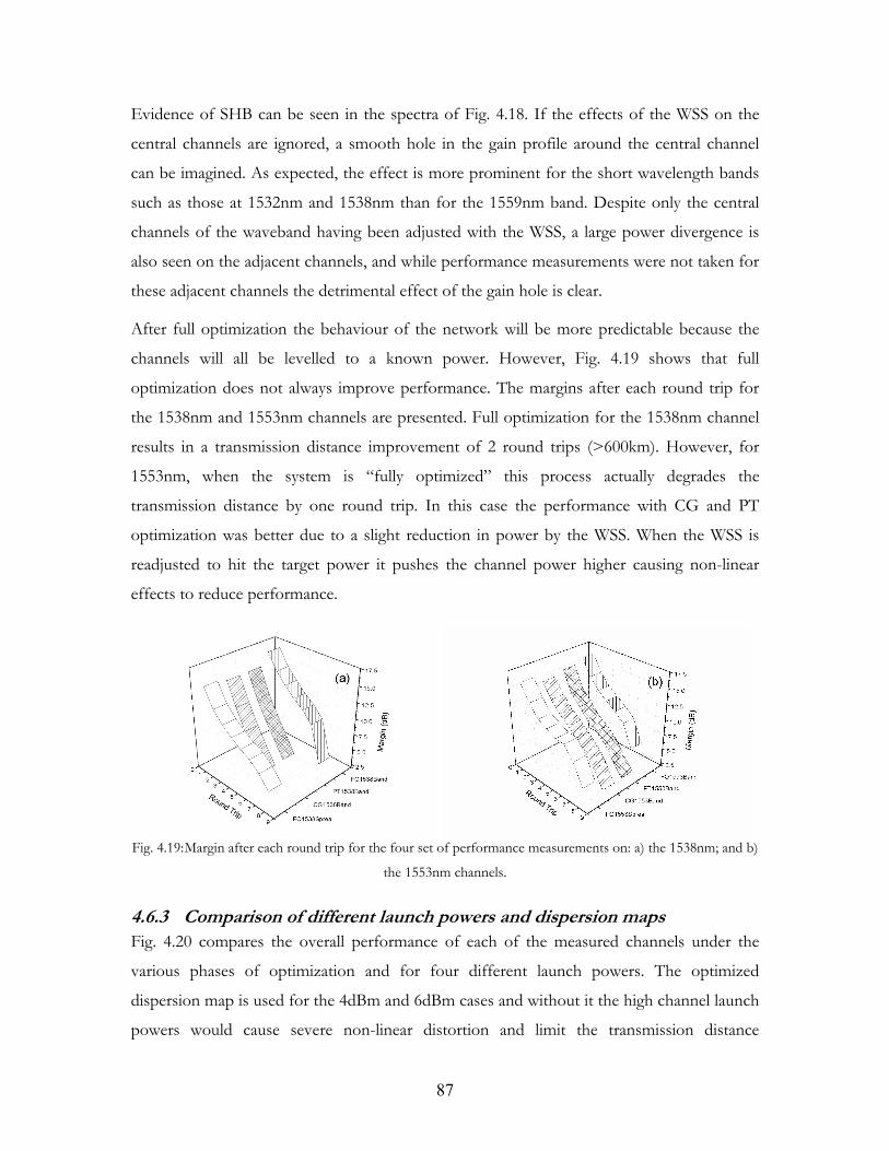
87
Evidence of SHB can be seen in the spectra of Fig. 4.18. If the effects of the WSS on the
central channels are ignored, a smooth hole in the gain profile around the central channel
can be imagined. As expected, the effect is more prominent for the short wavelength bands
such as those at 1532nm and 1538nm than for the 1559nm band. Despite only the central
channels of the waveband having been adjusted with the WSS, a large power divergence is
also seen on the adjacent channels, and while performance measurements were not taken for
these adjacent channels the detrimental effect of the gain hole is clear.
After full optimization the behaviour of the network will be more predictable because the
channels will all be levelled to a known power. However, Fig. 4.19 shows that full
optimization does not always improve performance. The margins after each round trip for
the 1538nm and 1553nm channels are presented. Full optimization for the 1538nm channel
results in a transmission distance improvement of 2 round trips (>600km). However, for
1553nm, when the system is “fully optimized” this process actually degrades the
transmission distance by one round trip. In this case the performance with CG and PT
optimization was better due to a slight reduction in power by the WSS. When the WSS is
readjusted to hit the target power it pushes the channel power higher causing non-linear
effects to reduce performance.
Fig. 4.19: Margin after each round trip for the four set of performance measurements on: a) the 1538nm; and b)
the 1553nm channels.
4.6.3 Comparison of different launch powers and dispersion maps Fig. 4.20 compares the overall performance of each of the measured channels under the
various phases of optimization and for four different launch powers. The optimized
dispersion map is used for the 4dBm and 6dBm cases and without it the high channel launch
powers would cause severe non-linear distortion and limit the transmission distance
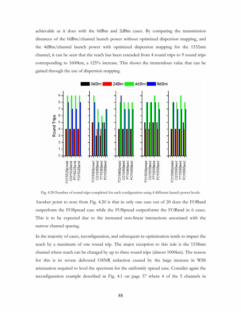
88
achievable as it does with the 0dBm and 2dBm cases. By comparing the transmission
distances of the 0dBm/channel launch power without optimized dispersion mapping, and
the 4dBm/channel launch power with optimized dispersion mapping for the 1532nm
channel, it can be seen that the reach has been extended from 4 round trips to 9 round trips
corresponding to 1600km, a 125% increase. This shows the tremendous value that can be
gained through the use of dispersion mapping.
Fig. 4.20: Number of round trips completed for each configuration using 4 different launch power levels.
Another point to note from Fig. 4.20 is that in only one case out of 20 does the FOBand
outperform the FOSpread case while the FOSpread outperforms the FOBand in 6 cases.
This is to be expected due to the increased non-linear interactions associated with the
narrow channel spacing.
In the majority of cases, reconfiguration, and subsequent re-optimization tends to impact the
reach by a maximum of one round trip. The major exception to this rule is the 1538nm
channel where reach can be changed by up to three round trips (almost 1000km). The reason
for this is its severe delivered OSNR reduction caused by the large increase in WSS
attenuation required to level the spectrum for the uniformly spread case. Consider again the
reconfiguration example described in Fig. 4.1 on page 57 where 4 of the 5 channels in
89
Configuration 2 required re-routing, but the 1538nm channel was to stay on its current path.
A configuration change from Configuration 2 to Configuration 4 (FO1538Spread to
CG1538Band) for this purpose causes an initial reduction in possible transmission distance
of up to 960km for the 1538nm data channel. Only when this new configuration is fully
optimized will the 1538nm channel reach its intended destination once more. This post
reconfiguration reach reduction has serious implications for reconfigurable networks.
4.7 Conclusion In current WDM networks, when wavelengths are provisioned or reconfigured, the process
is slow and methodical and the system is monitored throughout to ensure that no adverse
effects occur. With greater levels of automation, and shorter connection times, this manual
monitoring process becomes unfeasible. The automatic switching of channels at network
nodes can result in significant performance degradation due to channel power divergence
caused by EDFA gain dynamics and the historical system arrangement. EDFAs in
reconfigurable networks operate with constant gain to prevent instabilities associated with
strong channel power coupling. EDFA control circuits can effectively maintain the total gain
in the presence of channel reconfiguration; however the wavelength dependent gain still
varies. The result of this gain error is that the system arrangement (including EDFA settings
and gain equalization settings) optimized for the initial configuration is non-ideal for the new
configuration. The motivation of the work detailed in this chapter was to demonstrate the
possible transmission problems which can be caused by channel reconfiguration and to
stimulate further study and development of techniques which can predict the post-
reconfiguration behaviour of the network based on amplifier gain models and known
historical network states.
In order to study these issues, a method was developed which allowed the study of constant
gain based networks using a constant power based circulating loop apparatus. A number of
extreme channel loading configurations were inspected during three phases of post
reconfiguration optimization and showed that immediately after reconfiguration
transmission performance could be severely affected by the wavelength dependent gain error
and the historical network state. Subsequent optimization of the network for the new
configuration normalized performance but the length of time that re-optimization takes
could result in a significant reduction in throughput. Results showed that in the worst case
90
studied, reconfiguration from a spread configuration to a waveband configuration caused a
reduction in transmission distance of 37.5% (3 round trips of the circulating loop) for a
channel at 1538nm. Subsequent re-optimization for the new configuration improved the
reach by 2 round trips. Of the five channels whose performance was measured it was shown
that the 1538nm channel suffered the largest penalties due to reconfiguration.
The remaining chapters of this thesis move away from slow reconfiguration, typical of OCS
where connections may last anywhere from minutes to months or even years, and towards
Optical Packet Switching (OPS), a much faster form of optical switching, where
reconfiguration takes place on timescales of the order of nanoseconds. Chapter 5 will
describe work which was carried out on fast tunable lasers, which represent one of the key
components required to enable OPS. In Chapter 6, a novel optical labelling scheme,
employing these tunable lasers will be detailed.
91
References [1] P. Morkel, ”Edge-to-Core Optical Switching in Metro Apps”, Lightwave Europe,
January 2008.
[2] A. Srivastava, Y. Sun, “Advances in Erbium Doped Fiber Amplifiers” Optical Fiber
Telecommunications, Vol IVA, I. P Kaminow and T. Li, Eds. San Diego, CA: Academic 2002.
[3] H. Chou and J. Stimple, "Inhomogeneous Gain Saturation of Erbium-Doped Fiber
Amplifiers," in Optical Amplifiers and Their Applications, Vol. 18 of 1995 OSA Technical
Digest Series (Optical Society of America, 1995), paper ThE1.
[4] J. W. Sulhoff, A. K. Srivastava, C. Wolf, Y. Sun, J. L. Zyskind, “Spectral-Hole
Burning in Erbium Doped Silica and Fluoride Fibers,” IEEE Photon. Tech. Lett. Vol 9, No 12,
Dec 1997, pp 1578-1579.
[5] G. Luo, J.L. Zyskind, J.A. Nagel, M.A. Ali, "Experimental and theoretical analysis of
relaxation-oscillations and spectral hole burning effects in all-optical gain-clamped EDFA's
for WDM networks," J. Lightwave Technol. , vol.16, no.4, pp.527-533, Apr 1998
[6] J.L Zyskind et al, “Fast Power Transients in Optically Amplified Multi-Wavelength
Networks”, Proc. Tech. Dig. Optic. Fiber Commun. OFC'96, San Jose, CA, paper 1996.
[7] C.R. Giles, E.Desurvire, "Modeling erbium-doped fiber amplifiers," J. Lightwave
Technol., vol.9, no.2, pp.271-283, 1991
[8] F. Shehadeh, R. S. Vodhanel, C. Gibbons, and M. Ali, “Comparison of gain control
techniques to stabilize EDFA's for WDM networks,” Proc. Tech. Dig. Optic. Fiber
Commun. OFC'96, San Jose, CA, paper WM8, 1996.
[9] M.I. Hayee, A.E. Willner, "Transmission penalties due to EDFA gain transients in
add-drop multiplexed WDM networks," IEEE Photon. Technol. Lett. , vol.11, no.7, pp.889-
891, Jul 1999
[10] D. Kilper, C. Chandrasekhar, and C. A. White, " Transient Gain Dynamics of
Cascaded Erbium Doped Fiber Amplifiers with Re-Configured Channel Loading," in
Optical Fiber Communication Conference and Exposition and The National Fiber Optic
92
Engineers Conference, Technical Digest (CD) (Optical Society of America, 2006), paper
OTuK6.
[11] C. R. Giles, E. Desurvire, and J. R. Simpson, "Transient gain and cross talk in
erbium-doped fiber amplifiers," Opt. Lett. 14, 880- (1989)
[12] A.K. Srivastava; Y. Sun; J.L. Zyskind; J.W. Sulhoff, "EDFA transient response to
channel loss in WDM transmission system," Photonics Technology Letters, IEEE , vol.9, no.3,
pp.386-388, March 1997
[13] J. L. Zyskind, Y. Sun, A. K. Srivastava, J. W. Sulhoff, A. J. Lucero, C. Wolf, and R.
W. Thach, "Fast Power Transients in Optically Amplified Multiwavelength Optical
Networks," in Optical Fiber Communication Conference, Vol. 2 of 1996 OSA Technical Digest
Series (Optical Society of America, 1996), paper PD31.
[14] Y. Sun, A.K Srivastava, J.L. Zyskind, J.W. Sulhoff, C. Wolf, R.W. Tkach, "Fast
power transients in WDM optical networks with cascaded EDFAs ," Electronics Letters ,
vol.33, no.4, pp.313-314, 13 Feb 1997
[15] A.D. Ellis, R.M. Percival, A. Lord, W.A. Stallard, "Automatic gain control in
cascaded erbium doped fibre amplifier systems," Electronics Letters , vol.27, no.3, pp.193-195,
31 Jan 1991
[16] A. K. Srivastava, et al "Fast Gain Control in an Erbium-Doped Fiber Amplifier," in
Optical Amplifiers and Their Applications, R. Jopson, K. Stubkjaer, and M. Suyama, eds., Vol. 5
of OSA Trends in Optics and Photonics Series (Optical Society of America, 1996), paper
PP4.
[17] J.L. Jackel, D. Richards, "All-optical stabilization of cascaded multichannel erbium-
doped fiber amplifiers with changing numbers of channels," Optical Fiber Communication. OFC
97., Conference on , vol., no., pp.84-85, 16-21 Feb 1997
[18] M. Zirngibl, "Gain control in erbium-doped fibre amplifiers by an all-optical
feedback loop," Electronics Letters , vol.27, no.7, pp.560-561, 28 Mar 1991
[19] S. J. B. Yoo, W. Xin, L. D. Garrett, J. C. Young, G. Ellinas, J. C. Chiao, M. Rauch, J.
E. Baran, B. Meagher, H. Leblanc, and G.-K. Chang, “Observation of prolonged power
93
transients in a reconfigurable multiwavelength network and their suppression by gain-
clamping of optical amplifiers,” IEEE Photon. Technol. Lett., vol. 10, pp. 1659–1661, 1989.
[20] D.C Kilper, C.A. White, S. Chandrasekhar, "Control of Channel Power Instabilities
in Constant-Gain Amplified Transparent Networks Using Scalable Mesh Scheduling,"
Lightwave Technology, Journal of , vol.26, no.1, pp.108-113, Jan.1, 2008
[21] D.C. Kilper, S. Chandrasekhar, C.A White, "Transient gain dynamics of cascaded
erbium doped fiber amplifiers with re-configured channel loading," Optical Fiber
Communication Conference, 2006 and the 2006 National Fiber Optic Engineers Conference. OFC 2006 ,
vol., no., pp. 3 pp.-, 5-10 March 2006
[22] A. Gnauck, R. M. Jopson, “Dispersion Compensation for Optical Fibre Systems”
Optical Fiber Telecommunications, Vol IIIA, I. P Kaminow and T. Koch, Eds. San Diego, CA:
Academic 1997.
[23] F. Forgheiri, R. W. Tkach, A. R. Chraplyvy, “Fibre Nonlinearities and their impact
on transmission systems” Optical Fiber Telecommunications, Vol IIIA, I. P Kaminow and T.
Koch, Eds. San Diego, CA: Academic 1997.
[24] T. Naito, T. Terahara, T. Chikama, M. Suyama, "Four 5-Gb/s WDM transmission
over 4760-km straight-line using pre- and post-dispersion compensation and FWM cross talk
reduction," Optical Fiber Communications, 1996. OFC '96 , vol., no., pp. 182-183, 25 Feb.-1
March 1996
[25] D. Marcuse, “Selected Topics in the Theory of Telecommunications Fibers” Optical
Fiber Telecommunications, Vol II, S. E Miller and I. P Kaminow, Eds. San Diego, CA: Academic
1988.
[26] P. Bayvel, R. Killey, “Nonlinear Optical Effects in WDM transmission” Optical Fiber
Telecommunications, Vol IVB, I. P Kaminow and T. Li, Eds. San Diego, CA: Academic 1997.
[27] G. Belloti, A. Bertaina, S. Bigo, “Impact of residual dispersion on SPM-related power
margins in 10Gb/s-based systems using standard SMF” Proc. ECOC ’98, vol. 1, pp 681-682.
[28] G.P. Agrawal, Nonlinear Fiber Optics, Academic Press, San Diego, CA, USA, 1997.
94
[29] F. Forghieri, R.W. Tkach, A.R. Chraplyvy, "WDM systems with unequally spaced
channels," Lightwave Technology, Journal of , vol.13, no.5, pp.889-897, May 1995
[30] C. Vinegoni, M. Karlsson, M. Petersson, H. Sunnerud, "The statistics of polarization-
dependent loss in a recirculating loop," Lightwave Technology, Journal of , vol.22, no.4, pp. 968-
976, April 2004
[31] S. Kartalopoulos, DWDM: Networks, Devices and Technology, Wiley, NJ, USA, 2003.
[32] N. S. Bergano and C. R. Davidson, “Circulating loop transmission experiments for
the study of long haul transmission systems using erbium-doped fiber amplifiers,” J.
Lightwave Technol., vol. 13, pp. 1553–1561, May 1995.
[33] S. Chandrasekhar, D. Kilper, “Using testbeds for optically-transparent mesh network
experimentation” Lasers & Electro-Optics Society, IEEE Oct. 2006 Page(s):771 – 772
[34] P. Peloso, D. Penninckx, M. Prunaire, and L. Noirie: Optical transparency of a
heterogeneous pan-European network, J. Lightwave Technol., vol. 22, pp. 242-248, 2004.
[35] D. Kilper, S. Chandrasekhar, E. Burrows, L. L. Buhl, and J. Centanni: Local
dispersion map deviations in metro-regional transmission investigated using a dynamically
re-configurable re-circulating loop, in Proc. OFC/NFOEC 2007, paper OThL5.
[36] T. Yoshikawa, K. Okamura, E. Otani, T. Okaniwa, T. Uchino, M. Fukushima, and
N. Kagi, "WDM burst mode signal amplification by cascaded EDFAs with transient
control," Opt. Express 14, 4650-4655 (2006)
[37] C. Fürst, R. Hartung, J.-P. Elbers, C. Glingener, “Impact of Spectral Hole Burning
and Raman Effect in Transparent Optical Networks”, Proc of the European Conference on Optical
Communications, (ECOC 2003), Paper Tu:4.2.5, Rimini, Italy, Sept 21-25 2003.
Chapter 5 – Characterization of Tunable Lasers for use in Reconfigurable Optical
Networks
While the previous chapter was concerned with slow reconfiguration in Optical Circuit
Switched (OCS) mesh networks, the remainder of this thesis focuses on faster methods of
optical switching. This chapter is concerned with Fast Tunable Lasers (FTLs), which are
seen as a key component for future optical networks. More specifically, the chapter describes
Tunable Lasers (TLs) and details some experimental work carried out to examine their
suitability for deployment in Optical Packet Switching (OPS) and optical burst switching
(OBS) Wavelength Division Multiplexing (WDM) networks. The chapter begins by
discussing the roles of the tunable laser (TL) in WDM networks and the different properties
they must exhibit to fulfil these roles. Sections 5.3 to 5.4 provide background information
regarding TLs and the basics of their operation. In Sections 5.6, 5.7, and 5.8 the discussion
becomes more focused. Electronically tuned laser diodes are discussed, including specific
lasers which are essentially static but do exhibit some tunability, and also the structures used
to fabricate widely tunable lasers. The final two sections then detail two individual types of
widely tunable laser, namely the Sampled Grating Distributed Bragg reflector (SG-DBR) and
the tunable Slotted Fabry-Pérot (SFP) along with experimental work which was carried out
to characterise them.
5.1 Tunable Lasers - Applications Tunable lasers find application in many diverse fields, from astronomy to medicine, but this
chapter focuses on their applications in telecommunications. The two major applications are
inventory reduction/sparing and reconfiguration.
5.1.1 Inventory Reduction Prior to the commercial availability of widely tunable lasers, telecommunications carriers
were obliged to carry large inventories of laser diodes at every WDM channel in their system
in case of failure of a laser in the field. As WDM networks can often consist of 128 channels
or more, inventory maintenance quickly becomes cumbersome. Lasers which can be tuned
96
to any wavelength channel on the ITU allow the inventory size to be reduced considerably
which represents a logistical, as well as a financial benefit.
5.1.2 Reconfiguration TLs will play a part in enabling a number of the features available in reconfigurable optical
networks such as dynamic provisioning and bandwidth allocation, lightpath routing,
protection and restoration, and burst and packet switching. They will be employed in tunable
wavelength converters and transponders within network nodes and also in transmitter
subsystems. For provisioning new wavelengths in a system, where more bandwidth is
required, tunable lasers in the transmitter can be used to provide channels at any available
wavelength. In this case, tuning speeds do not need to be very fast because the channel will
be turned on slowly, while monitoring the network for problems. In addition, the channel
will likely be in place for a long time, so switching times of seconds are adequate.
For dynamic reconfigurability and fault restoration, in transparent systems which are being
deployed currently, reconfiguration is generally performed using space switching techniques,
rather than wavelength switching due to the fact that the majority of lasers in the
transmitters are static devices. Sub-second switching times are required in order to minimize
data loss and maximize network throughput. In protection systems, carriers have long been
offering their customers 50ms protection with SONET/SDH systems so switching times of
the order of a few tens of milliseconds would be suitable. Wavelength switching could be
enabled in these networks through the installation of tunable lasers and AWGs as the
switching fabric, or by replacing the current static transmitters with tunable ones; however it
seems more likely that wavelength switching will be commercially deployed in future systems
such as OBS and OPS which require much faster switching times. In conjunction with a
passive Arrayed Waveguide Grating (AWG), TLs can be used to build an optical router in
which the light is directed to a certain output port by tuning the laser’s wavelength. With
switching speeds in the low nanoseconds available with the state of the art tunable lasers,
such optical routers are suitable for OBS and OPS applications. In these systems the
transmitters in the edge nodes of the core network use FTLs as their source. The FTL is
tuned to a certain wavelength depending on the output port onto which the packet or burst
should be placed. In the core nodes, data is not detected and retransmitted; rather it remains
in optical format throughout the network. As such, tunable transmitters are not required,
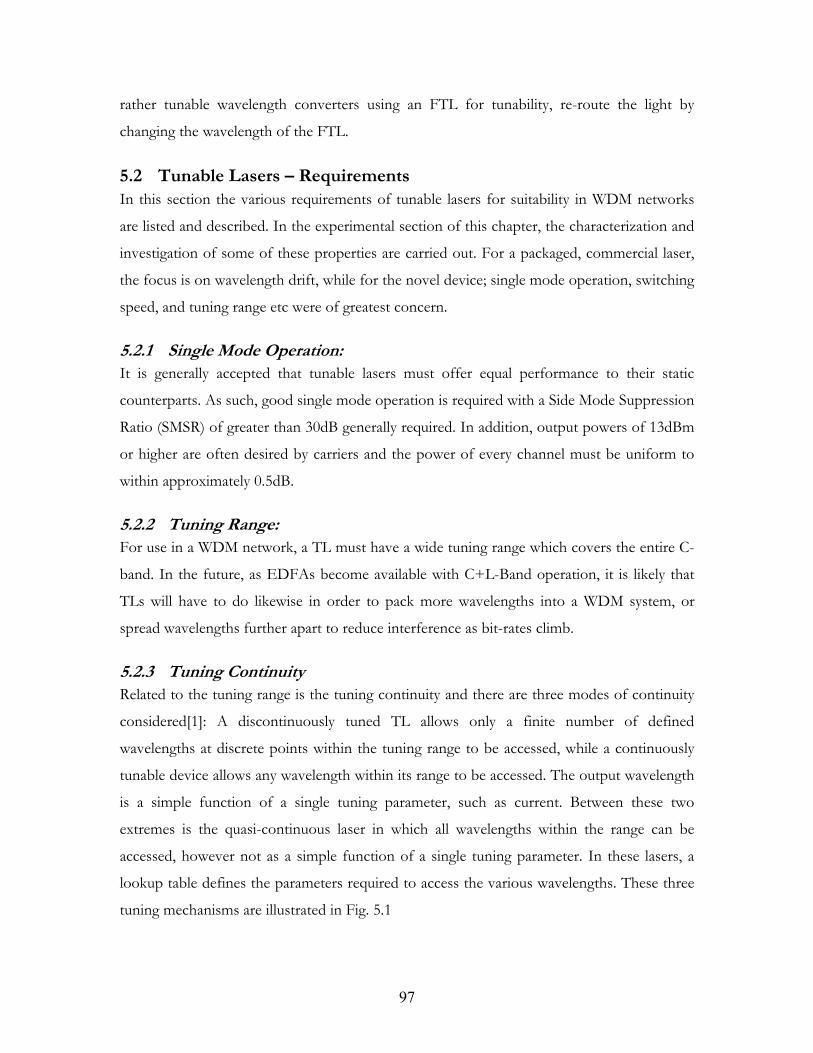
97
rather tunable wavelength converters using an FTL for tunability, re-route the light by
changing the wavelength of the FTL.
5.2 Tunable Lasers – Requirements In this section the various requirements of tunable lasers for suitability in WDM networks
are listed and described. In the experimental section of this chapter, the characterization and
investigation of some of these properties are carried out. For a packaged, commercial laser,
the focus is on wavelength drift, while for the novel device; single mode operation, switching
speed, and tuning range etc were of greatest concern.
5.2.1 Single Mode Operation: It is generally accepted that tunable lasers must offer equal performance to their static
counterparts. As such, good single mode operation is required with a Side Mode Suppression
Ratio (SMSR) of greater than 30dB generally required. In addition, output powers of 13dBm
or higher are often desired by carriers and the power of every channel must be uniform to
within approximately 0.5dB.
5.2.2 Tuning Range: For use in a WDM network, a TL must have a wide tuning range which covers the entire C-
band. In the future, as EDFAs become available with C+L-Band operation, it is likely that
TLs will have to do likewise in order to pack more wavelengths into a WDM system, or
spread wavelengths further apart to reduce interference as bit-rates climb.
5.2.3 Tuning Continuity Related to the tuning range is the tuning continuity and there are three modes of continuity
considered[1]: A discontinuously tuned TL allows only a finite number of defined
wavelengths at discrete points within the tuning range to be accessed, while a continuously
tunable device allows any wavelength within its range to be accessed. The output wavelength
is a simple function of a single tuning parameter, such as current. Between these two
extremes is the quasi-continuous laser in which all wavelengths within the range can be
accessed, however not as a simple function of a single tuning parameter. In these lasers, a
lookup table defines the parameters required to access the various wavelengths. These three
tuning mechanisms are illustrated in Fig. 5.1
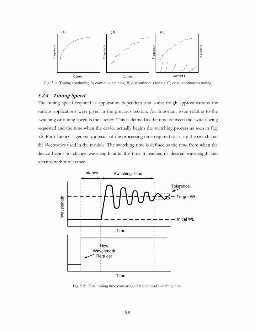
98
Fig. 5.1: Tuning continuity; A) continuous tuning; B) discontinuous tuning; C) quasi-continuous tuning
5.2.4 Tuning Speed The tuning speed required is application dependent and some rough approximations for
various applications were given in the previous section. An important issue relating to the
switching or tuning speed is the latency. This is defined as the time between the switch being
requested and the time when the device actually begins the switching process as seen in Fig.
5.2. Poor latency is generally a result of the processing time required to set up the switch and
the electronics used in the module. The switching time is defined as the time from when the
device begins to change wavelength until the time it reaches its desired wavelength and
remains within tolerance.
Fig. 5.2: Total tuning time consisting of latency and switching time.
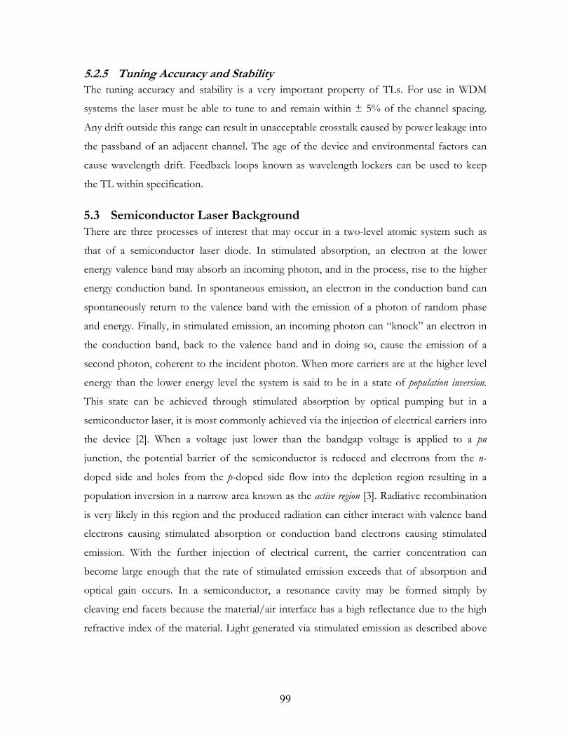
99
5.2.5 Tuning Accuracy and Stability The tuning accuracy and stability is a very important property of TLs. For use in WDM
systems the laser must be able to tune to and remain within ± 5% of the channel spacing.
Any drift outside this range can result in unacceptable crosstalk caused by power leakage into
the passband of an adjacent channel. The age of the device and environmental factors can
cause wavelength drift. Feedback loops known as wavelength lockers can be used to keep
the TL within specification.
5.3 Semiconductor Laser Background There are three processes of interest that may occur in a two-level atomic system such as
that of a semiconductor laser diode. In stimulated absorption, an electron at the lower
energy valence band may absorb an incoming photon, and in the process, rise to the higher
energy conduction band. In spontaneous emission, an electron in the conduction band can
spontaneously return to the valence band with the emission of a photon of random phase
and energy. Finally, in stimulated emission, an incoming photon can “knock” an electron in
the conduction band, back to the valence band and in doing so, cause the emission of a
second photon, coherent to the incident photon. When more carriers are at the higher level
energy than the lower energy level the system is said to be in a state of population inversion.
This state can be achieved through stimulated absorption by optical pumping but in a
semiconductor laser, it is most commonly achieved via the injection of electrical carriers into
the device [2]. When a voltage just lower than the bandgap voltage is applied to a pn
junction, the potential barrier of the semiconductor is reduced and electrons from the n-
doped side and holes from the p-doped side flow into the depletion region resulting in a
population inversion in a narrow area known as the active region [3]. Radiative recombination
is very likely in this region and the produced radiation can either interact with valence band
electrons causing stimulated absorption or conduction band electrons causing stimulated
emission. With the further injection of electrical current, the carrier concentration can
become large enough that the rate of stimulated emission exceeds that of absorption and
optical gain occurs. In a semiconductor, a resonance cavity may be formed simply by
cleaving end facets because the material/air interface has a high reflectance due to the high
refractive index of the material. Light generated via stimulated emission as described above
100
gets reflected by the facets back into the cavity and can stimulate further emission of
photons leading to amplification [4].
In semiconductor lasers the resonance cavity can generally support a number of longitudinal
modes, the spacing of which depends on the length of the cavity. Although lasing will only
occur at modes which lie within the gain spectrum of the material as shown in Fig. 5.3,
generally the gain spectrum is wide enough and the longitudinal mode spacing narrow
enough that the result is a multi-mode laser output. Lasers with multi-mode outputs suffer
badly from dispersion and are unsuitable for WDM systems. Methods have been developed,
therefore to encourage single mode output and these will be described in section 5.4.
Fig. 5.3: A number of longitudinal modes are present but lasing only occurs for modes which lie within the
gain spectrum of the material
5.4 Single Mode Operation Theoretically, the simplest way to achieve single mode operation is to reduce the cavity
length until only a single longitudinal mode is supported. The main problem with this
technique in practice is that short cavity lengths result in low output powers. Vertical cavity
surface emitting lasers (VCSELs) employ the short cavity technique but to less of an
extreme. The cavity is generally long enough to support multiple modes, but short enough
that these modes are widely spaced, such that only a single mode will sit under the gain curve
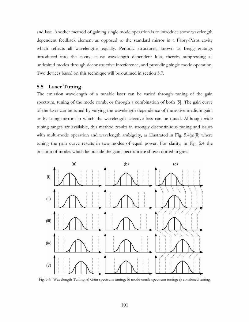
101
and lase. Another method of gaining single mode operation is to introduce some wavelength
dependent feedback element as opposed to the standard mirror in a Fabry-Pérot cavity
which reflects all wavelengths equally. Periodic structures, known as Bragg gratings
introduced into the cavity, cause wavelength dependent loss, thereby suppressing all
undesired modes through deconstructive interference, and providing single mode operation.
Two devices based on this technique will be outlined in section 5.7.
5.5 Laser Tuning The emission wavelength of a tunable laser can be varied through tuning of the gain
spectrum, tuning of the mode comb, or through a combination of both [5]. The gain curve
of the laser can be tuned by varying the wavelength dependence of the active medium gain,
or by using mirrors in which the wavelength selective loss can be tuned. Although wide
tuning ranges are available, this method results in strongly discontinuous tuning and issues
with multi-mode operation and wavelength ambiguity, as illustrated in Fig. 5.4(a)(ii) where
tuning the gain curve results in two modes of equal power. For clarity, in Fig. 5.4 the
position of modes which lie outside the gain spectrum are shown dotted in grey.
Fig. 5.4: Wavelength Tuning; a) Gain spectrum tuning; b) mode-comb spectrum tuning; c) combined tuning.
102
The second method of tuning is achieved by varying the spectrum of the mode comb. This
is achieved by varying the phase condition in the cavity via adjustments to the length of the
cavity, which is the method used in an External Cavity Laser (ECL), or via adjustments to
the refractive index in the cavity. This method is shown in Fig. 5.4(b). It results in
continuous tuning with a tuning range equal to the mode spacing. Tuning further than one
mode spacing results in a mode hop that cancels out the wavelength shift. Clearly this
method offers the advantage of continuous tuning but is limited in the range it can tune over
due to the shape of the static gain curve. Through simultaneous variation of both the gain
spectrum and the mode-comb spectrum, quasi-continuous tuning over a wide range can be
achieved as depicted in Fig. 5.4(c). Here, the dashed lines between Fig. 5.4(c) (i) - (v) show
that the mode has been tuned across to the point of a mode hop. Between these points,
continuous tuning is available giving quasi-continuous tuning across the entire band.
5.6 Laser Diode Tuning Methods As discussed in the previous section, variation of the gain spectrum, together with variation
of the mode comb spectrum allows for quasi-continuous tuning of the laser across a large
range of wavelengths. The mode comb is varied by changing the phase condition in the
cavity, either via a change in cavity length, or via a change in the refractive index in the
cavity. In external cavity lasers (ECLs) the cavity length is varied mechanically in order to
achieve this phase condition change. However this results in relatively slow tuning times. In
order to achieve very fast tuning times, the refractive index method must be used. With
regard to the gain spectrum variation, in general a Bragg grating is used to give wavelength
selective loss such that lasing only occurs at the wavelength of minimum loss. This
wavelength is set by the pitch of the grating, and the effective refractive index of the grating.
Because the pitch of the grating is fixed in the fabrication process, only the refractive index
can be easily used to tune the gain spectrum. Therefore in order to tune the output
wavelength, it is necessary to vary the refractive index of a phase element and/or an
amplitude element of the laser. In semiconductors refractive index tuning can be achieved
using field effects, thermal control and carrier injection.
The electric field method, although extremely fast, only causes a small change in the
refractive index of a semiconductor, and as such limits the tuning range available. Thermal
refractive index changes allow wider tuning than are available with electric field variation,
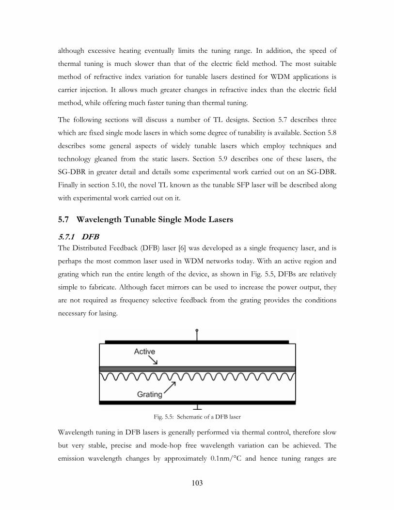
103
although excessive heating eventually limits the tuning range. In addition, the speed of
thermal tuning is much slower than that of the electric field method. The most suitable
method of refractive index variation for tunable lasers destined for WDM applications is
carrier injection. It allows much greater changes in refractive index than the electric field
method, while offering much faster tuning than thermal tuning.
The following sections will discuss a number of TL designs. Section 5.7 describes three
which are fixed single mode lasers in which some degree of tunability is available. Section 5.8
describes some general aspects of widely tunable lasers which employ techniques and
technology gleaned from the static lasers. Section 5.9 describes one of these lasers, the
SG-DBR in greater detail and details some experimental work carried out on an SG-DBR.
Finally in section 5.10, the novel TL known as the tunable SFP laser will be described along
with experimental work carried out on it.
5.7 Wavelength Tunable Single Mode Lasers
5.7.1 DFB The Distributed Feedback (DFB) laser [6] was developed as a single frequency laser, and is
perhaps the most common laser used in WDM networks today. With an active region and
grating which run the entire length of the device, as shown in Fig. 5.5, DFBs are relatively
simple to fabricate. Although facet mirrors can be used to increase the power output, they
are not required as frequency selective feedback from the grating provides the conditions
necessary for lasing.
Fig. 5.5: Schematic of a DFB laser
Wavelength tuning in DFB lasers is generally performed via thermal control, therefore slow
but very stable, precise and mode-hop free wavelength variation can be achieved. The
emission wavelength changes by approximately 0.1nm/°C and hence tuning ranges are
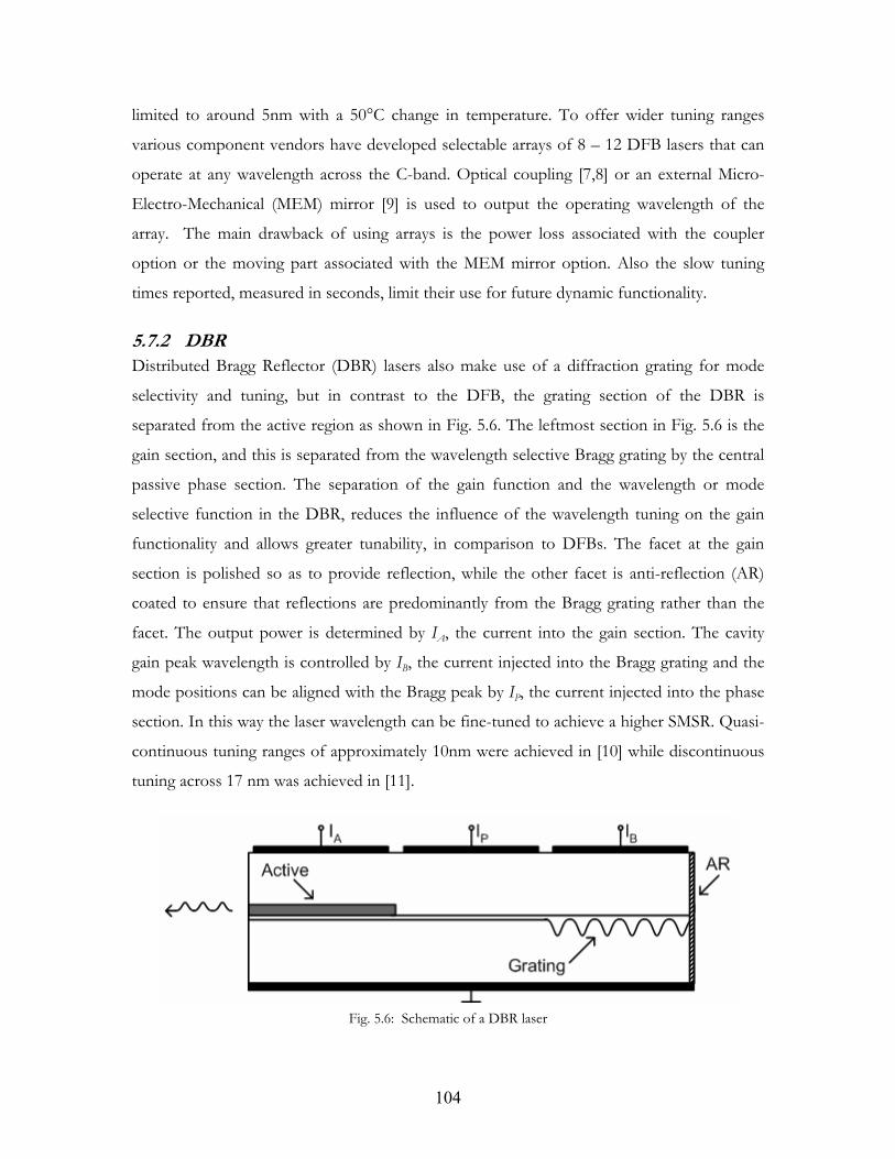
104
limited to around 5nm with a 50°C change in temperature. To offer wider tuning ranges
various component vendors have developed selectable arrays of 8 – 12 DFB lasers that can
operate at any wavelength across the C-band. Optical coupling [7,8] or an external Micro-
Electro-Mechanical (MEM) mirror [9] is used to output the operating wavelength of the
array. The main drawback of using arrays is the power loss associated with the coupler
option or the moving part associated with the MEM mirror option. Also the slow tuning
times reported, measured in seconds, limit their use for future dynamic functionality.
5.7.2 DBR Distributed Bragg Reflector (DBR) lasers also make use of a diffraction grating for mode
selectivity and tuning, but in contrast to the DFB, the grating section of the DBR is
separated from the active region as shown in Fig. 5.6. The leftmost section in Fig. 5.6 is the
gain section, and this is separated from the wavelength selective Bragg grating by the central
passive phase section. The separation of the gain function and the wavelength or mode
selective function in the DBR, reduces the influence of the wavelength tuning on the gain
functionality and allows greater tunability, in comparison to DFBs. The facet at the gain
section is polished so as to provide reflection, while the other facet is anti-reflection (AR)
coated to ensure that reflections are predominantly from the Bragg grating rather than the
facet. The output power is determined by IA, the current into the gain section. The cavity
gain peak wavelength is controlled by IB, the current injected into the Bragg grating and the
mode positions can be aligned with the Bragg peak by IP, the current injected into the phase
section. In this way the laser wavelength can be fine-tuned to achieve a higher SMSR. Quasi-
continuous tuning ranges of approximately 10nm were achieved in [10] while discontinuous
tuning across 17 nm was achieved in [11].
Fig. 5.6: Schematic of a DBR laser
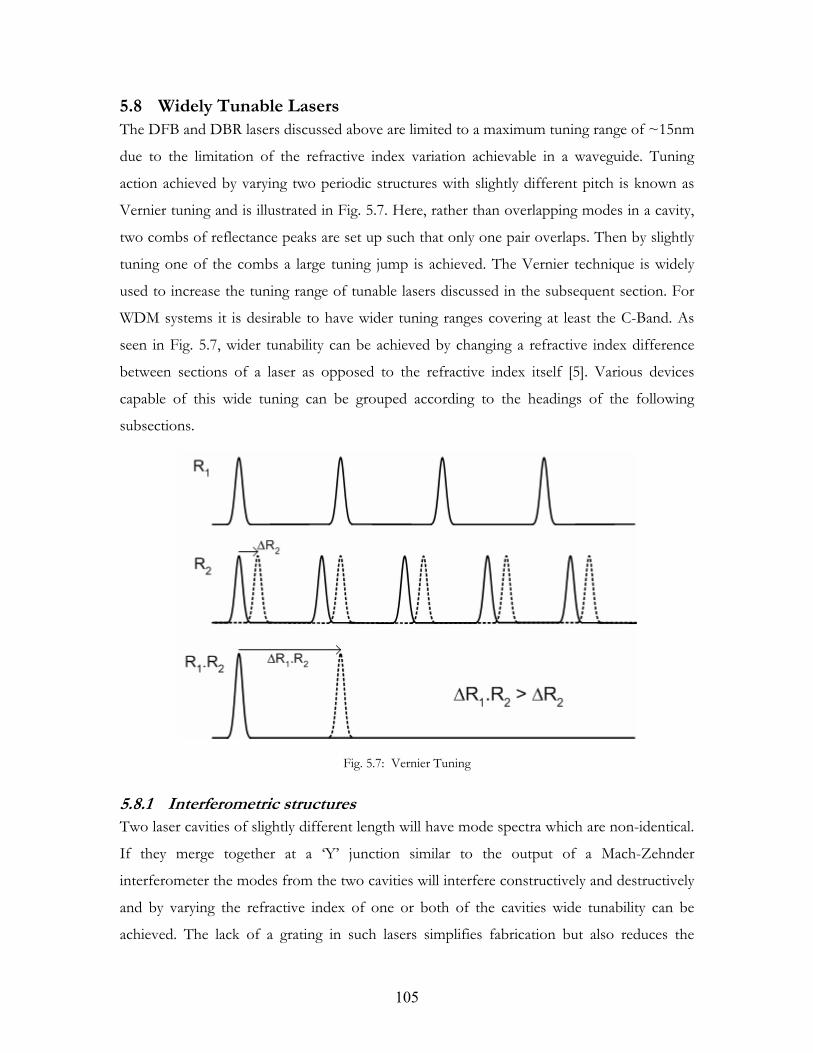
105
5.8 Widely Tunable Lasers The DFB and DBR lasers discussed above are limited to a maximum tuning range of ~15nm
due to the limitation of the refractive index variation achievable in a waveguide. Tuning
action achieved by varying two periodic structures with slightly different pitch is known as
Vernier tuning and is illustrated in Fig. 5.7. Here, rather than overlapping modes in a cavity,
two combs of reflectance peaks are set up such that only one pair overlaps. Then by slightly
tuning one of the combs a large tuning jump is achieved. The Vernier technique is widely
used to increase the tuning range of tunable lasers discussed in the subsequent section. For
WDM systems it is desirable to have wider tuning ranges covering at least the C-Band. As
seen in Fig. 5.7, wider tunability can be achieved by changing a refractive index difference
between sections of a laser as opposed to the refractive index itself [5]. Various devices
capable of this wide tuning can be grouped according to the headings of the following
subsections.
Fig. 5.7: Vernier Tuning
5.8.1 Interferometric structures Two laser cavities of slightly different length will have mode spectra which are non-identical.
If they merge together at a ‘Y’ junction similar to the output of a Mach-Zehnder
interferometer the modes from the two cavities will interfere constructively and destructively
and by varying the refractive index of one or both of the cavities wide tunability can be
achieved. The lack of a grating in such lasers simplifies fabrication but also reduces the
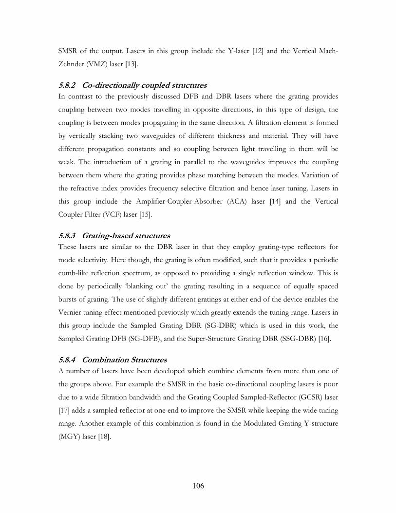
106
SMSR of the output. Lasers in this group include the Y-laser [12] and the Vertical Mach-
Zehnder (VMZ) laser [13].
5.8.2 Co-directionally coupled structures In contrast to the previously discussed DFB and DBR lasers where the grating provides
coupling between two modes travelling in opposite directions, in this type of design, the
coupling is between modes propagating in the same direction. A filtration element is formed
by vertically stacking two waveguides of different thickness and material. They will have
different propagation constants and so coupling between light travelling in them will be
weak. The introduction of a grating in parallel to the waveguides improves the coupling
between them where the grating provides phase matching between the modes. Variation of
the refractive index provides frequency selective filtration and hence laser tuning. Lasers in
this group include the Amplifier-Coupler-Absorber (ACA) laser [14] and the Vertical
Coupler Filter (VCF) laser [15].
5.8.3 Grating-based structures These lasers are similar to the DBR laser in that they employ grating-type reflectors for
mode selectivity. Here though, the grating is often modified, such that it provides a periodic
comb-like reflection spectrum, as opposed to providing a single reflection window. This is
done by periodically ‘blanking out’ the grating resulting in a sequence of equally spaced
bursts of grating. The use of slightly different gratings at either end of the device enables the
Vernier tuning effect mentioned previously which greatly extends the tuning range. Lasers in
this group include the Sampled Grating DBR (SG-DBR) which is used in this work, the
Sampled Grating DFB (SG-DFB), and the Super-Structure Grating DBR (SSG-DBR) [16].
5.8.4 Combination Structures A number of lasers have been developed which combine elements from more than one of
the groups above. For example the SMSR in the basic co-directional coupling lasers is poor
due to a wide filtration bandwidth and the Grating Coupled Sampled-Reflector (GCSR) laser
[17] adds a sampled reflector at one end to improve the SMSR while keeping the wide tuning
range. Another example of this combination is found in the Modulated Grating Y-structure
(MGY) laser [18].
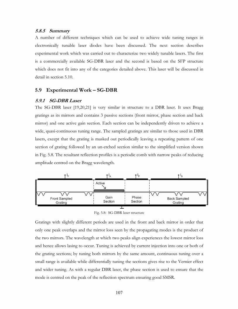
107
5.8.5 Summary A number of different techniques which can be used to achieve wide tuning ranges in
electronically tunable laser diodes have been discussed. The next section describes
experimental work which was carried out to characterize two widely tunable lasers. The first
is a commercially available SG-DBR laser and the second is based on the SFP structure
which does not fit into any of the categories detailed above. This laser will be discussed in
detail in section 5.10.
5.9 Experimental Work – SG-DBR
5.9.1 SG-DBR Laser The SG-DBR laser [19,20,21] is very similar in structure to a DBR laser. It uses Bragg
gratings as its mirrors and contains 3 passive sections (front mirror, phase section and back
mirror) and one active gain section. Each section can be independently driven to achieve a
wide, quasi-continuous tuning range. The sampled gratings are similar to those used in DBR
lasers, except that the grating is masked out periodically leaving a repeating pattern of one
section of grating followed by an un-etched section similar to the simplified version shown
in Fig. 5.8. The resultant reflection profiles is a periodic comb with narrow peaks of reducing
amplitude centred on the Bragg wavelength.
Fig. 5.8: SG-DBR laser structure
Gratings with slightly different periods are used in the front and back mirror in order that
only one peak overlaps and the mirror loss seen by the propagating modes is the product of
the two mirrors. The wavelength at which two peaks align experiences the lowest mirror loss
and hence allows lasing to occur. Tuning is achieved by current injection into one or both of
the grating sections; by tuning both mirrors by the same amount, continuous tuning over a
small range is available while differentially tuning the sections gives rise to the Vernier effect
and wider tuning. As with a regular DBR laser, the phase section is used to ensure that the
mode is centred on the peak of the reflection spectrum ensuring good SMSR.
108
The mid-chip positioning of the active gain section of SG-DBR lasers reduces the output
power achievable from them. In addition, because the front mirror may require high drive
currents to reach the outer wavelengths, a wavelength dependent loss can occur in this
section leading to an output power which varies for different channels. Uniform output
power can achieved through tuning of the gain section however gain section variations can
also affect the wavelength so more often a semiconductor optical amplifier (SOA) is
integrated with the SG-DBR for power control [22]. This SOA also serves as an output
blanking mechanism which blocks the laser emission and ensures that spurious modes are
not transmitted during a tuning/switching event.
5.9.2 Lookup Table The complex tuning current arrangements required to obtain quasi-continuous tuning from
an SG-DBR laser generally dictates that the laser tuning is controlled by a micro-processor
that accesses a lookup table containing the currents required for the three sections in order
to tune to a desired wavelength. A block diagram typical of a commercially available SG-
DBR laser is shown in Fig. 5.9.
Fig. 5.9: SG-DBR TL module with wavelength and power feedback control block diagram
The lookup table can be generated using simple experiments in which the light output is
coupled directly into an optical spectrum analyser (OSA). The gain and phase section
currents are then kept constant and the mirror currents are varied in order to obtain
information about the peak wavelength, output power and SMSR at each pair of mirror
currents. A sample wavelength map is shown in Fig. 5.10. Generally, such maps are
generated for a number of phase currents until each wavelength channel on the ITU grid can
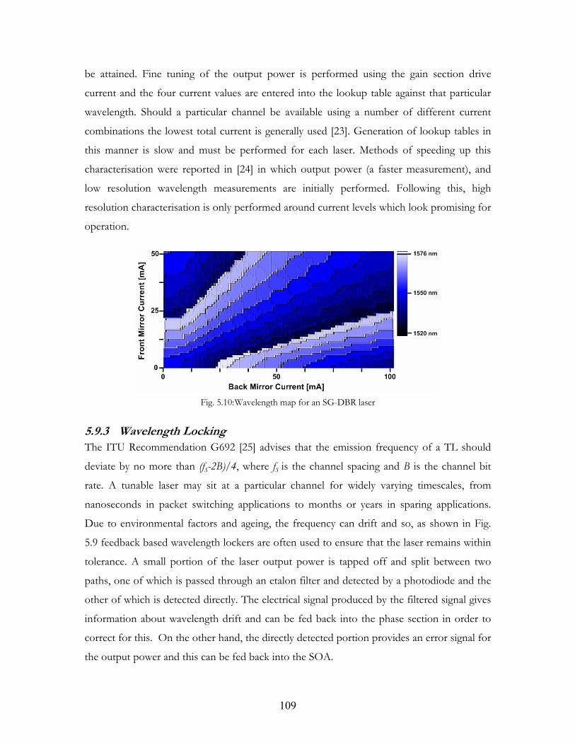
109
be attained. Fine tuning of the output power is performed using the gain section drive
current and the four current values are entered into the lookup table against that particular
wavelength. Should a particular channel be available using a number of different current
combinations the lowest total current is generally used [23]. Generation of lookup tables in
this manner is slow and must be performed for each laser. Methods of speeding up this
characterisation were reported in [24] in which output power (a faster measurement), and
low resolution wavelength measurements are initially performed. Following this, high
resolution characterisation is only performed around current levels which look promising for
operation.
Fig. 5.10: Wavelength map for an SG-DBR laser
5.9.3 Wavelength Locking The ITU Recommendation G692 [25] advises that the emission frequency of a TL should
deviate by no more than (fS-2B)/4, where fS is the channel spacing and B is the channel bit
rate. A tunable laser may sit at a particular channel for widely varying timescales, from
nanoseconds in packet switching applications to months or years in sparing applications.
Due to environmental factors and ageing, the frequency can drift and so, as shown in Fig.
5.9 feedback based wavelength lockers are often used to ensure that the laser remains within
tolerance. A small portion of the laser output power is tapped off and split between two
paths, one of which is passed through an etalon filter and detected by a photodiode and the
other of which is detected directly. The electrical signal produced by the filtered signal gives
information about wavelength drift and can be fed back into the phase section in order to
correct for this. On the other hand, the directly detected portion provides an error signal for
the output power and this can be fed back into the SOA.
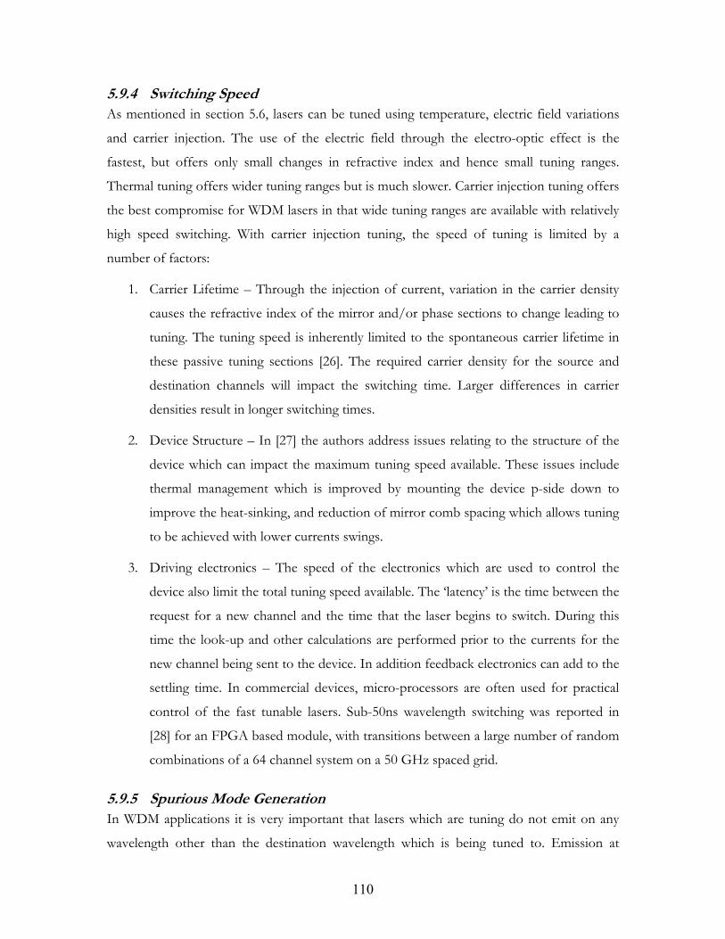
110
5.9.4 Switching Speed As mentioned in section 5.6, lasers can be tuned using temperature, electric field variations
and carrier injection. The use of the electric field through the electro-optic effect is the
fastest, but offers only small changes in refractive index and hence small tuning ranges.
Thermal tuning offers wider tuning ranges but is much slower. Carrier injection tuning offers
the best compromise for WDM lasers in that wide tuning ranges are available with relatively
high speed switching. With carrier injection tuning, the speed of tuning is limited by a
number of factors:
1. Carrier Lifetime – Through the injection of current, variation in the carrier density
causes the refractive index of the mirror and/or phase sections to change leading to
tuning. The tuning speed is inherently limited to the spontaneous carrier lifetime in
these passive tuning sections [26]. The required carrier density for the source and
destination channels will impact the switching time. Larger differences in carrier
densities result in longer switching times.
2. Device Structure – In [27] the authors address issues relating to the structure of the
device which can impact the maximum tuning speed available. These issues include
thermal management which is improved by mounting the device p-side down to
improve the heat-sinking, and reduction of mirror comb spacing which allows tuning
to be achieved with lower currents swings.
3. Driving electronics – The speed of the electronics which are used to control the
device also limit the total tuning speed available. The ‘latency’ is the time between the
request for a new channel and the time that the laser begins to switch. During this
time the look-up and other calculations are performed prior to the currents for the
new channel being sent to the device. In addition feedback electronics can add to the
settling time. In commercial devices, micro-processors are often used for practical
control of the fast tunable lasers. Sub-50ns wavelength switching was reported in
[28] for an FPGA based module, with transitions between a large number of random
combinations of a 64 channel system on a 50 GHz spaced grid.
5.9.5 Spurious Mode Generation In WDM applications it is very important that lasers which are tuning do not emit on any
wavelength other than the destination wavelength which is being tuned to. Emission at
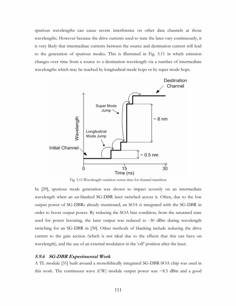
111
spurious wavelengths can cause severe interference on other data channels at those
wavelengths. However because the drive currents used to tune the laser vary continuously, it
is very likely that intermediate currents between the source and destination current will lead
to the generation of spurious modes. This is illustrated in Fig. 5.11 in which emission
changes over time from a source to a destination wavelength via a number of intermediate
wavelengths which may be reached by longitudinal mode hops or by super mode hops.
Fig. 5.11: Wavelength variation versus time for channel transition
In [29], spurious mode generation was shown to impact severely on an intermediate
wavelength when an un-blanked SG-DBR laser switched across it. Often, due to the low
output power of SG-DBRs already mentioned, an SOA is integrated with the SG-DBR in
order to boost output power. By reducing the SOA bias condition, from the saturated state
used for power boosting, the laser output was reduced to -30 dBm during wavelength
switching for an SG-DBR in [30]. Other methods of blanking include reducing the drive
current to the gain section (which is not ideal due to the effects that this can have on
wavelength), and the use of an external modulator in the ‘off’ position after the laser.
5.9.6 SG-DBR Experimental Work A TL module [31] built around a monolithically integrated SG-DBR-SOA chip was used in
this work. The continuous wave (CW) module output power was ~8.5 dBm and a good
112
SMSR (>40dB) was measured for all channels. The tuning range was 33.4 nm and within this
range 85 channels spaced by 50 GHz were available as shown in Fig. 5.12. The module could
be programmed to switch between any set of these 50GHz channels. For the first 50ns after
a switch was initiated the emission on spurious wavelengths was possible and so the SOA
was used for blanking for 60ns after the switch is initiated. After this time the laser was
guaranteed to be within ±15GHz of its intended frequency. The wavelength locker was then
used to reduce the frequency variation and after 200ns the emission frequency was
guaranteed to be, and to stay within ±2.5GHz of the target frequency.
Fig. 5.12: Overlaid channel spectra from the SG-DBR module showing 85 50GHz spaced channels with SMSR
> 40dB
5.9.7 Frequency Drift Experiment As carriers try to pack more data into less bandwidth by reducing the WDM channel spacing
or increasing the data rate per channel, the wavelength drift requirements of tunable lasers
used in the system become increasingly stringent. In systems with channel spacing of 50GHz
or less even a small drift could cause the laser to enter the pass-band of an adjacent channel
leading to cross-channel interference. In this section, experimental analysis of the frequency
drift of one of the SG-DBR laser modules described above is detailed. The instantaneous
frequency drift of a TL module immediately after the blanking period is measured with high
resolution using two different techniques. Initial characterisation is performed using an
optical filter as a frequency discriminator. The results obtained are then verified using an
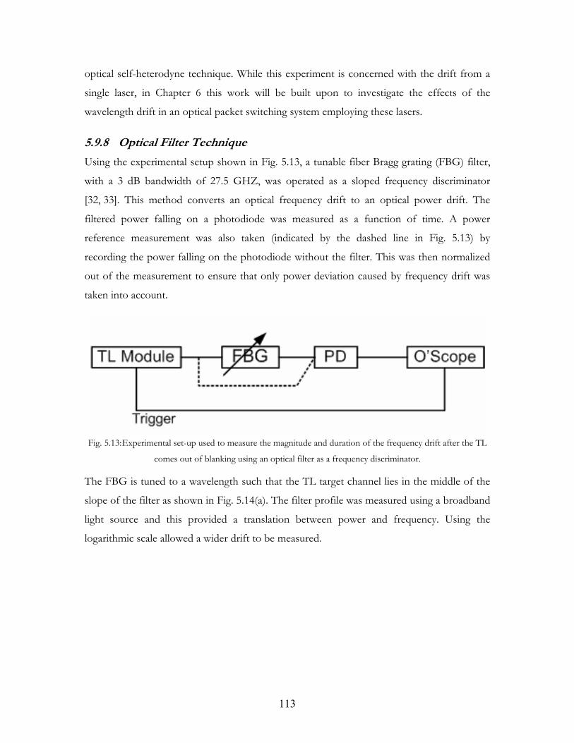
113
optical self-heterodyne technique. While this experiment is concerned with the drift from a
single laser, in Chapter 6 this work will be built upon to investigate the effects of the
wavelength drift in an optical packet switching system employing these lasers.
5.9.8 Optical Filter Technique Using the experimental setup shown in Fig. 5.13, a tunable fiber Bragg grating (FBG) filter,
with a 3 dB bandwidth of 27.5 GHZ, was operated as a sloped frequency discriminator
[32, 33]. This method converts an optical frequency drift to an optical power drift. The
filtered power falling on a photodiode was measured as a function of time. A power
reference measurement was also taken (indicated by the dashed line in Fig. 5.13) by
recording the power falling on the photodiode without the filter. This was then normalized
out of the measurement to ensure that only power deviation caused by frequency drift was
taken into account.
Fig. 5.13: Experimental set-up used to measure the magnitude and duration of the frequency drift after the TL
comes out of blanking using an optical filter as a frequency discriminator.
The FBG is tuned to a wavelength such that the TL target channel lies in the middle of the
slope of the filter as shown in Fig. 5.14(a). The filter profile was measured using a broadband
light source and this provided a translation between power and frequency. Using the
logarithmic scale allowed a wider drift to be measured.
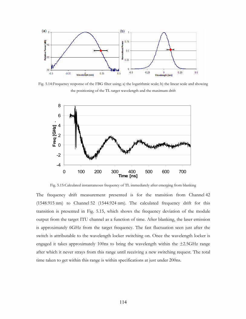
114
Fig. 5.14: Frequency response of the FBG filter using; a) the logarithmic scale; b) the linear scale and showing
the positioning of the TL target wavelength and the maximum drift
-4
-2
0
2
4
6
8
0 100 200 300 400 500 600 700Time [ns]
Freq
[GH
z] .
Fig. 5.15: Calculated instantaneous frequency of TL immediately after emerging from blanking
The frequency drift measurement presented is for the transition from Channel 42
(1548.915 nm) to Channel 52 (1544.924 nm). The calculated frequency drift for this
transition is presented in Fig. 5.15, which shows the frequency deviation of the module
output from the target ITU channel as a function of time. After blanking, the laser emission
is approximately 6GHz from the target frequency. The fast fluctuation seen just after the
switch is attributable to the wavelength locker switching on. Once the wavelength locker is
engaged it takes approximately 100ns to bring the wavelength within the ±2.5GHz range
after which it never strays from this range until receiving a new switching request. The total
time taken to get within this range is within specifications at just under 200ns.
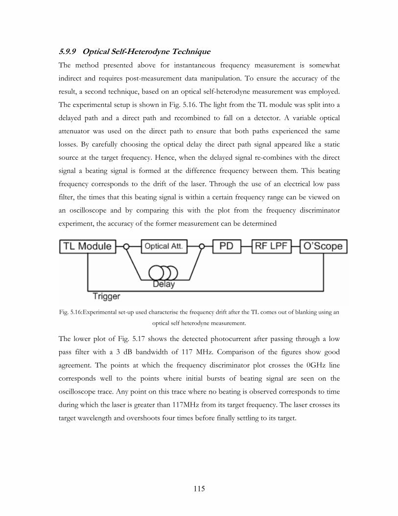
115
5.9.9 Optical Self-Heterodyne Technique The method presented above for instantaneous frequency measurement is somewhat
indirect and requires post-measurement data manipulation. To ensure the accuracy of the
result, a second technique, based on an optical self-heterodyne measurement was employed.
The experimental setup is shown in Fig. 5.16. The light from the TL module was split into a
delayed path and a direct path and recombined to fall on a detector. A variable optical
attenuator was used on the direct path to ensure that both paths experienced the same
losses. By carefully choosing the optical delay the direct path signal appeared like a static
source at the target frequency. Hence, when the delayed signal re-combines with the direct
signal a beating signal is formed at the difference frequency between them. This beating
frequency corresponds to the drift of the laser. Through the use of an electrical low pass
filter, the times that this beating signal is within a certain frequency range can be viewed on
an oscilloscope and by comparing this with the plot from the frequency discriminator
experiment, the accuracy of the former measurement can be determined
Fig. 5.16: Experimental set-up used characterise the frequency drift after the TL comes out of blanking using an
optical self heterodyne measurement.
The lower plot of Fig. 5.17 shows the detected photocurrent after passing through a low
pass filter with a 3 dB bandwidth of 117 MHz. Comparison of the figures show good
agreement. The points at which the frequency discriminator plot crosses the 0GHz line
corresponds well to the points where initial bursts of beating signal are seen on the
oscilloscope trace. Any point on this trace where no beating is observed corresponds to time
during which the laser is greater than 117MHz from its target frequency. The laser crosses its
target wavelength and overshoots four times before finally settling to its target.
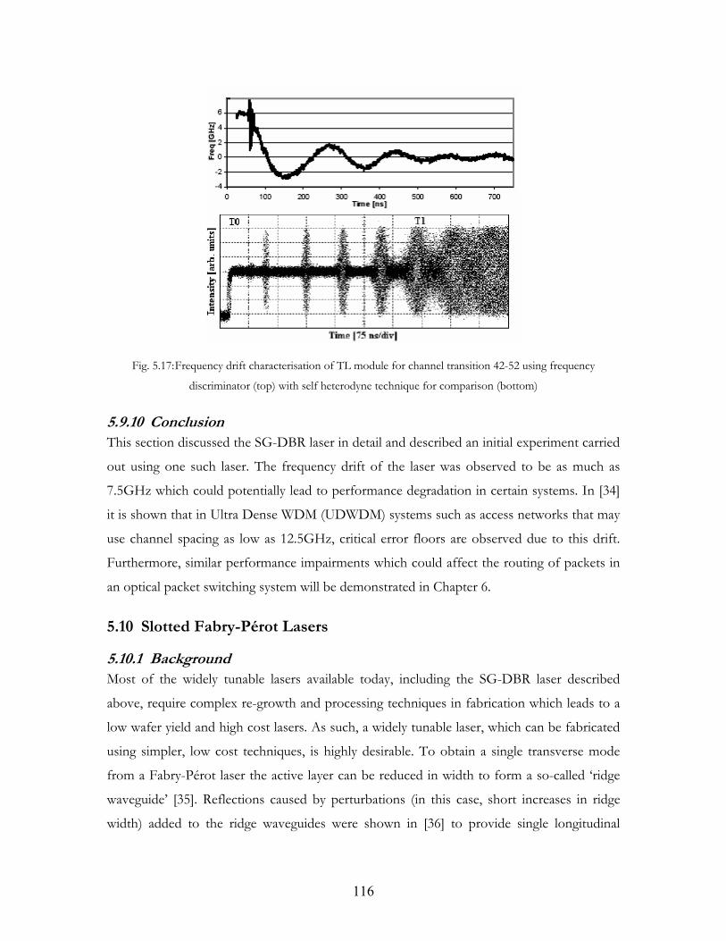
116
Fig. 5.17: Frequency drift characterisation of TL module for channel transition 42-52 using frequency
discriminator (top) with self heterodyne technique for comparison (bottom)
5.9.10 Conclusion This section discussed the SG-DBR laser in detail and described an initial experiment carried
out using one such laser. The frequency drift of the laser was observed to be as much as
7.5GHz which could potentially lead to performance degradation in certain systems. In [34]
it is shown that in Ultra Dense WDM (UDWDM) systems such as access networks that may
use channel spacing as low as 12.5GHz, critical error floors are observed due to this drift.
Furthermore, similar performance impairments which could affect the routing of packets in
an optical packet switching system will be demonstrated in Chapter 6.
5.10 Slotted Fabry-Pérot Lasers
5.10.1 Background Most of the widely tunable lasers available today, including the SG-DBR laser described
above, require complex re-growth and processing techniques in fabrication which leads to a
low wafer yield and high cost lasers. As such, a widely tunable laser, which can be fabricated
using simpler, low cost techniques, is highly desirable. To obtain a single transverse mode
from a Fabry-Pérot laser the active layer can be reduced in width to form a so-called ‘ridge
waveguide’ [35]. Reflections caused by perturbations (in this case, short increases in ridge
width) added to the ridge waveguides were shown in [36] to provide single longitudinal
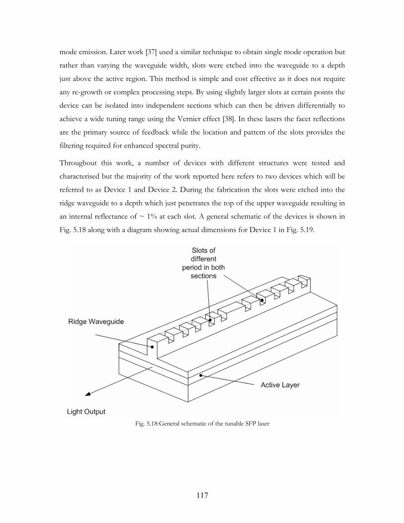
117
mode emission. Later work [37] used a similar technique to obtain single mode operation but
rather than varying the waveguide width, slots were etched into the waveguide to a depth
just above the active region. This method is simple and cost effective as it does not require
any re-growth or complex processing steps. By using slightly larger slots at certain points the
device can be isolated into independent sections which can then be driven differentially to
achieve a wide tuning range using the Vernier effect [38]. In these lasers the facet reflections
are the primary source of feedback while the location and pattern of the slots provides the
filtering required for enhanced spectral purity.
Throughout this work, a number of devices with different structures were tested and
characterised but the majority of the work reported here refers to two devices which will be
referred to as Device 1 and Device 2. During the fabrication the slots were etched into the
ridge waveguide to a depth which just penetrates the top of the upper waveguide resulting in
an internal reflectance of ~ 1% at each slot. A general schematic of the devices is shown in
Fig. 5.18 along with a diagram showing actual dimensions for Device 1 in Fig. 5.19.
Fig. 5.18: General schematic of the tunable SFP laser
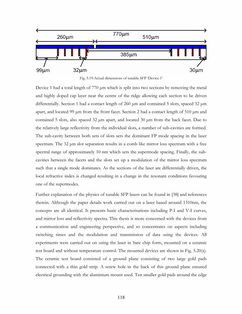
118
Fig. 5.19: Actual dimensions of tunable SFP ‘Device 1’
Device 1 had a total length of 770 µm which is split into two sections by removing the metal
and highly doped cap layer near the centre of the ridge allowing each section to be driven
differentially. Section 1 had a contact length of 260 µm and contained 5 slots, spaced 32 µm
apart, and located 99 µm from the front facet. Section 2 had a contact length of 510 µm and
contained 5 slots, also spaced 32 µm apart, and located 30 µm from the back facet. Due to
the relatively large reflectivity from the individual slots, a number of sub-cavities are formed.
The sub-cavity between both sets of slots sets the dominant FP mode spacing in the laser
spectrum. The 32 µm slot separation results in a comb like mirror loss spectrum with a free
spectral range of approximately 10 nm which sets the supermode spacing. Finally, the sub-
cavities between the facets and the slots set up a modulation of the mirror loss spectrum
such that a single mode dominates. As the sections of the laser are differentially driven, the
local refractive index is changed resulting in a change in the resonant conditions favouring
one of the supermodes.
Further explanation of the physics of tunable SFP lasers can be found in [38] and references
therein. Although the paper details work carried out on a laser based around 1310nm, the
concepts are all identical. It presents basic characterisations including P-I and V-I curves,
and mirror loss and reflectivity spectra. This thesis is more concerned with the devices from
a communication and engineering perspective, and so concentrates on aspects including
switching times and the modulation and transmission of data using the devices. All
experiments were carried out on using the laser in bare chip form, mounted on a ceramic
test board and without temperature control. The mounted devices are shown in Fig. 5.20(a).
The ceramic test board consisted of a ground plane consisting of two large gold pads
connected with a thin gold strip. A screw hole in the back of this ground plane ensured
electrical grounding with the aluminium mount used. Ten smaller gold pads around the edge
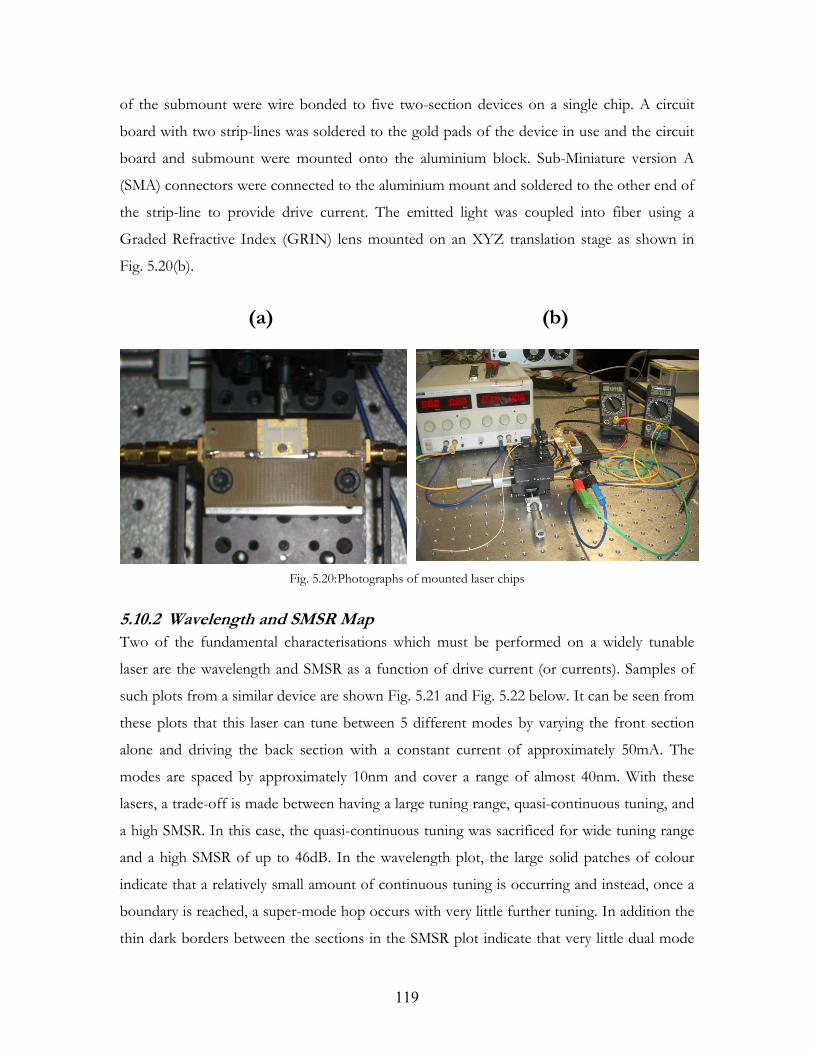
119
of the submount were wire bonded to five two-section devices on a single chip. A circuit
board with two strip-lines was soldered to the gold pads of the device in use and the circuit
board and submount were mounted onto the aluminium block. Sub-Miniature version A
(SMA) connectors were connected to the aluminium mount and soldered to the other end of
the strip-line to provide drive current. The emitted light was coupled into fiber using a
Graded Refractive Index (GRIN) lens mounted on an XYZ translation stage as shown in
Fig. 5.20(b).
(a) (b)
Fig. 5.20: Photographs of mounted laser chips
5.10.2 Wavelength and SMSR Map Two of the fundamental characterisations which must be performed on a widely tunable
laser are the wavelength and SMSR as a function of drive current (or currents). Samples of
such plots from a similar device are shown Fig. 5.21 and Fig. 5.22 below. It can be seen from
these plots that this laser can tune between 5 different modes by varying the front section
alone and driving the back section with a constant current of approximately 50mA. The
modes are spaced by approximately 10nm and cover a range of almost 40nm. With these
lasers, a trade-off is made between having a large tuning range, quasi-continuous tuning, and
a high SMSR. In this case, the quasi-continuous tuning was sacrificed for wide tuning range
and a high SMSR of up to 46dB. In the wavelength plot, the large solid patches of colour
indicate that a relatively small amount of continuous tuning is occurring and instead, once a
boundary is reached, a super-mode hop occurs with very little further tuning. In addition the
thin dark borders between the sections in the SMSR plot indicate that very little dual mode
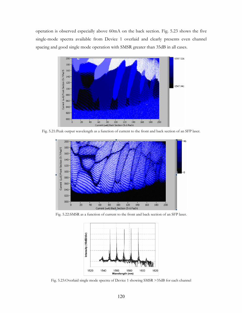
120
operation is observed especially above 60mA on the back section. Fig. 5.23 shows the five
single-mode spectra available from Device 1 overlaid and clearly presents even channel
spacing and good single mode operation with SMSR greater than 35dB in all cases.
Fig. 5.21: Peak output wavelength as a function of current to the front and back section of an SFP laser.
Fig. 5.22: SMSR as a function of current to the front and back section of an SFP laser.
Fig. 5.23: Overlaid single mode spectra of Device 1 showing SMSR >35dB for each channel
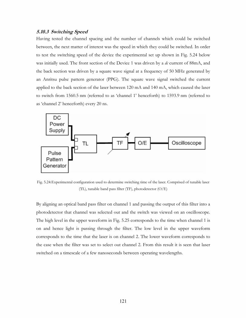
121
5.10.3 Switching Speed Having tested the channel spacing and the number of channels which could be switched
between, the next matter of interest was the speed in which they could be switched. In order
to test the switching speed of the device the experimental set up shown in Fig. 5.24 below
was initially used. The front section of the Device 1 was driven by a dc current of 88mA, and
the back section was driven by a square wave signal at a frequency of 50 MHz generated by
an Anritsu pulse pattern generator (PPG). The square wave signal switched the current
applied to the back section of the laser between 120 mA and 140 mA, which caused the laser
to switch from 1560.5 nm (referred to as ‘channel 1’ henceforth) to 1593.9 nm (referred to
as ‘channel 2’ henceforth) every 20 ns.
Fig. 5.24: Experimental configuration used to determine switching time of the laser. Comprised of tunable laser
(TL), tunable band pass filter (TF), photodetector (O/E)
By aligning an optical band pass filter on channel 1 and passing the output of this filter into a
photodetector that channel was selected out and the switch was viewed on an oscilloscope.
The high level in the upper waveform in Fig. 5.25 corresponds to the time when channel 1 is
on and hence light is passing through the filter. The low level in the upper waveform
corresponds to the time that the laser is on channel 2. The lower waveform corresponds to
the case when the filter was set to select out channel 2. From this result it is seen that laser
switched on a timescale of a few nanoseconds between operating wavelengths.
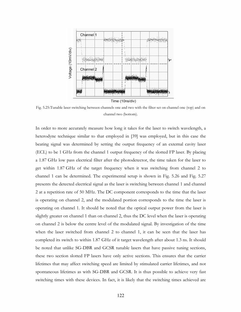
122
Fig. 5.25: Tunable laser switching between channels one and two with the filter set on channel one (top) and on
channel two (bottom).
In order to more accurately measure how long it takes for the laser to switch wavelength, a
heterodyne technique similar to that employed in [39] was employed, but in this case the
beating signal was determined by setting the output frequency of an external cavity laser
(ECL) to be 1 GHz from the channel 1 output frequency of the slotted FP laser. By placing
a 1.87 GHz low pass electrical filter after the photodetector, the time taken for the laser to
get within 1.87 GHz of the target frequency when it was switching from channel 2 to
channel 1 can be determined. The experimental setup is shown in Fig. 5.26 and Fig. 5.27
presents the detected electrical signal as the laser is switching between channel 1 and channel
2 at a repetition rate of 50 MHz. The DC component corresponds to the time that the laser
is operating on channel 2, and the modulated portion corresponds to the time the laser is
operating on channel 1. It should be noted that the optical output power from the laser is
slightly greater on channel 1 than on channel 2, thus the DC level when the laser is operating
on channel 2 is below the centre level of the modulated signal. By investigation of the time
when the laser switched from channel 2 to channel 1, it can be seen that the laser has
completed its switch to within 1.87 GHz of it target wavelength after about 1.3 ns. It should
be noted that unlike SG-DBR and GCSR tunable lasers that have passive tuning sections,
these two section slotted FP lasers have only active sections. This ensures that the carrier
lifetimes that may affect switching speed are limited by stimulated carrier lifetimes, and not
spontaneous lifetimes as with SG-DBR and GCSR. It is thus possible to achieve very fast
switching times with these devices. In fact, it is likely that the switching times achieved are
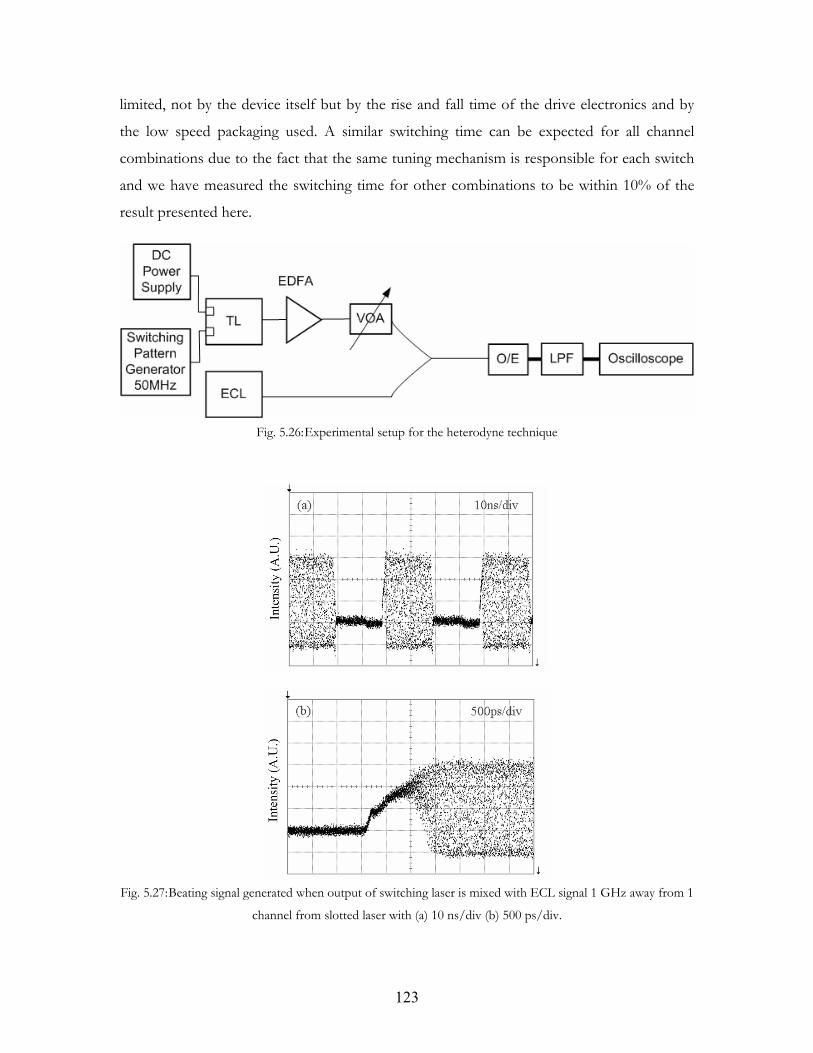
123
limited, not by the device itself but by the rise and fall time of the drive electronics and by
the low speed packaging used. A similar switching time can be expected for all channel
combinations due to the fact that the same tuning mechanism is responsible for each switch
and we have measured the switching time for other combinations to be within 10% of the
result presented here.
Fig. 5.26: Experimental setup for the heterodyne technique
Fig. 5.27: Beating signal generated when output of switching laser is mixed with ECL signal 1 GHz away from 1
channel from slotted laser with (a) 10 ns/div (b) 500 ps/div.
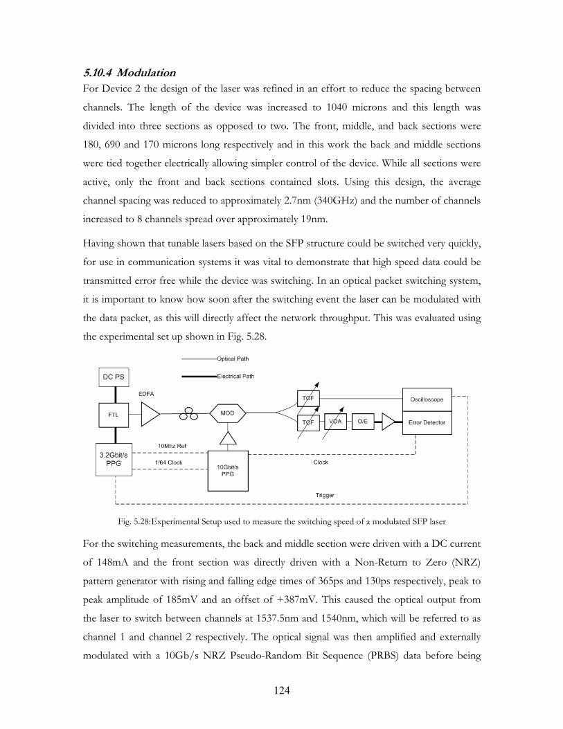
124
5.10.4 Modulation For Device 2 the design of the laser was refined in an effort to reduce the spacing between
channels. The length of the device was increased to 1040 microns and this length was
divided into three sections as opposed to two. The front, middle, and back sections were
180, 690 and 170 microns long respectively and in this work the back and middle sections
were tied together electrically allowing simpler control of the device. While all sections were
active, only the front and back sections contained slots. Using this design, the average
channel spacing was reduced to approximately 2.7nm (340GHz) and the number of channels
increased to 8 channels spread over approximately 19nm.
Having shown that tunable lasers based on the SFP structure could be switched very quickly,
for use in communication systems it was vital to demonstrate that high speed data could be
transmitted error free while the device was switching. In an optical packet switching system,
it is important to know how soon after the switching event the laser can be modulated with
the data packet, as this will directly affect the network throughput. This was evaluated using
the experimental set up shown in Fig. 5.28.
Fig. 5.28: Experimental Setup used to measure the switching speed of a modulated SFP laser
For the switching measurements, the back and middle section were driven with a DC current
of 148mA and the front section was directly driven with a Non-Return to Zero (NRZ)
pattern generator with rising and falling edge times of 365ps and 130ps respectively, peak to
peak amplitude of 185mV and an offset of +387mV. This caused the optical output from
the laser to switch between channels at 1537.5nm and 1540nm, which will be referred to as
channel 1 and channel 2 respectively. The optical signal was then amplified and externally
modulated with a 10Gb/s NRZ Pseudo-Random Bit Sequence (PRBS) data before being
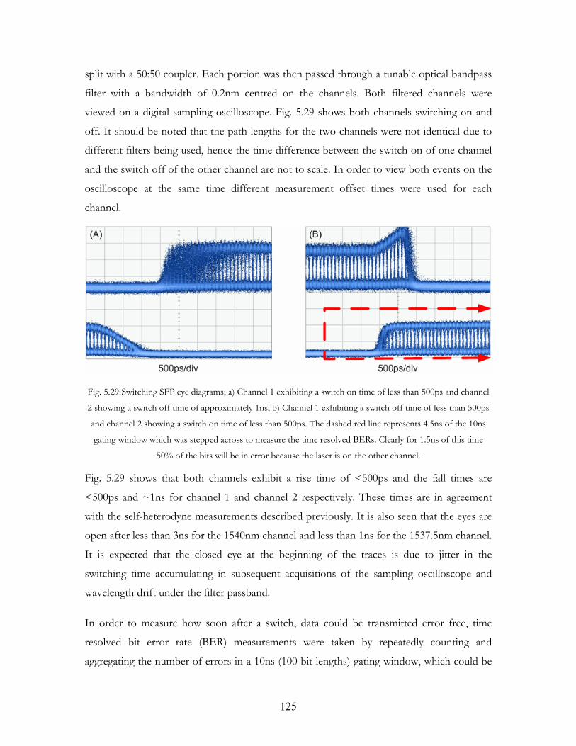
125
split with a 50:50 coupler. Each portion was then passed through a tunable optical bandpass
filter with a bandwidth of 0.2nm centred on the channels. Both filtered channels were
viewed on a digital sampling oscilloscope. Fig. 5.29 shows both channels switching on and
off. It should be noted that the path lengths for the two channels were not identical due to
different filters being used, hence the time difference between the switch on of one channel
and the switch off of the other channel are not to scale. In order to view both events on the
oscilloscope at the same time different measurement offset times were used for each
channel.
Fig. 5.29: Switching SFP eye diagrams; a) Channel 1 exhibiting a switch on time of less than 500ps and channel
2 showing a switch off time of approximately 1ns; b) Channel 1 exhibiting a switch off time of less than 500ps
and channel 2 showing a switch on time of less than 500ps. The dashed red line represents 4.5ns of the 10ns
gating window which was stepped across to measure the time resolved BERs. Clearly for 1.5ns of this time
50% of the bits will be in error because the laser is on the other channel.
Fig. 5.29 shows that both channels exhibit a rise time of <500ps and the fall times are
<500ps and ~1ns for channel 1 and channel 2 respectively. These times are in agreement
with the self-heterodyne measurements described previously. It is also seen that the eyes are
open after less than 3ns for the 1540nm channel and less than 1ns for the 1537.5nm channel.
It is expected that the closed eye at the beginning of the traces is due to jitter in the
switching time accumulating in subsequent acquisitions of the sampling oscilloscope and
wavelength drift under the filter passband.
In order to measure how soon after a switch, data could be transmitted error free, time
resolved bit error rate (BER) measurements were taken by repeatedly counting and
aggregating the number of errors in a 10ns (100 bit lengths) gating window, which could be
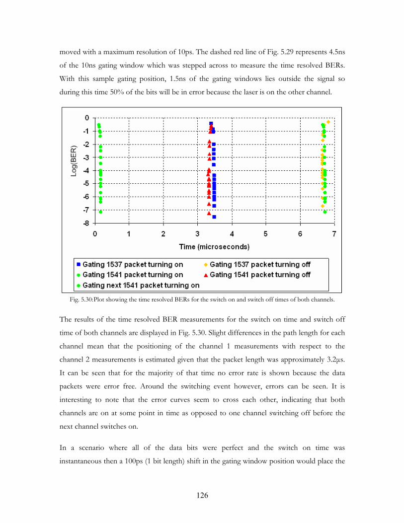
126
moved with a maximum resolution of 10ps. The dashed red line of Fig. 5.29 represents 4.5ns
of the 10ns gating window which was stepped across to measure the time resolved BERs.
With this sample gating position, 1.5ns of the gating windows lies outside the signal so
during this time 50% of the bits will be in error because the laser is on the other channel.
Fig. 5.30: Plot showing the time resolved BERs for the switch on and switch off times of both channels.
The results of the time resolved BER measurements for the switch on time and switch off
time of both channels are displayed in Fig. 5.30. Slight differences in the path length for each
channel mean that the positioning of the channel 1 measurements with respect to the
channel 2 measurements is estimated given that the packet length was approximately 3.2µs.
It can be seen that for the majority of that time no error rate is shown because the data
packets were error free. Around the switching event however, errors can be seen. It is
interesting to note that the error curves seem to cross each other, indicating that both
channels are on at some point in time as opposed to one channel switching off before the
next channel switches on.
In a scenario where all of the data bits were perfect and the switch on time was
instantaneous then a 100ps (1 bit length) shift in the gating window position would place the
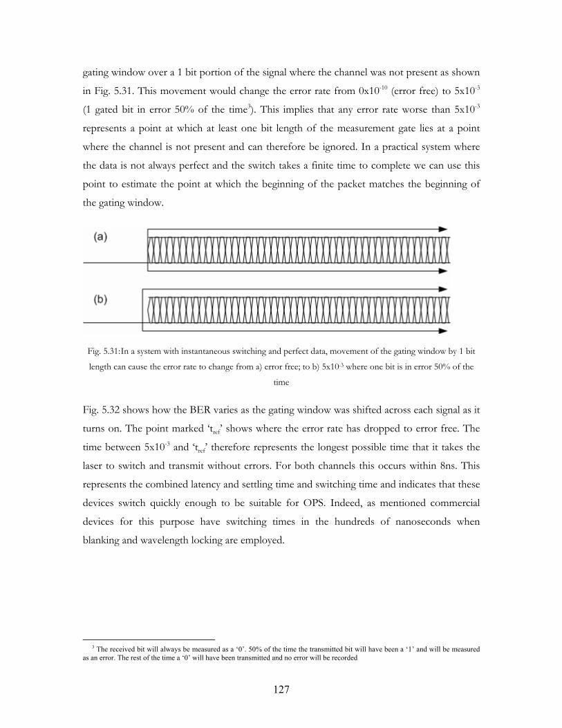
127
gating window over a 1 bit portion of the signal where the channel was not present as shown
in Fig. 5.31. This movement would change the error rate from 0x10-10 (error free) to 5x10⁻³
(1 gated bit in error 50% of the time3). This implies that any error rate worse than 5x10⁻³
represents a point at which at least one bit length of the measurement gate lies at a point
where the channel is not present and can therefore be ignored. In a practical system where
the data is not always perfect and the switch takes a finite time to complete we can use this
point to estimate the point at which the beginning of the packet matches the beginning of
the gating window.
Fig. 5.31: In a system with instantaneous switching and perfect data, movement of the gating window by 1 bit
length can cause the error rate to change from a) error free; to b) 5x10⁻³ where one bit is in error 50% of the
time
Fig. 5.32 shows how the BER varies as the gating window was shifted across each signal as it
turns on. The point marked ‘tref’ shows where the error rate has dropped to error free. The
time between 5x10⁻³ and ‘tref’ therefore represents the longest possible time that it takes the
laser to switch and transmit without errors. For both channels this occurs within 8ns. This
represents the combined latency and settling time and switching time and indicates that these
devices switch quickly enough to be suitable for OPS. Indeed, as mentioned commercial
devices for this purpose have switching times in the hundreds of nanoseconds when
blanking and wavelength locking are employed.
3 The received bit will always be measured as a ‘0’. 50% of the time the transmitted bit will have been a ‘1’ and will be measured
as an error. The rest of the time a ‘0’ will have been transmitted and no error will be recorded
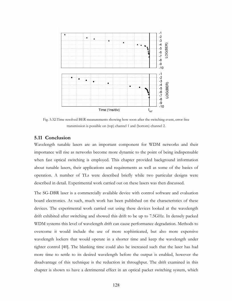
128
Fig. 5.32: Time resolved BER measurements showing how soon after the switching event, error free
transmission is possible on (top) channel 1 and (bottom) channel 2.
5.11 Conclusion Wavelength tunable lasers are an important component for WDM networks and their
importance will rise as networks become more dynamic to the point of being indispensable
when fast optical switching is employed. This chapter provided background information
about tunable lasers, their applications and requirements as well as some of the basics of
operation. A number of TLs were described briefly while two particular designs were
described in detail. Experimental work carried out on these lasers was then discussed.
The SG-DBR laser is a commercially available device with control software and evaluation
board electronics. As such, much work has been published on the characteristics of these
devices. The experimental work carried out using these devices looked at the wavelength
drift exhibited after switching and showed this drift to be up to 7.5GHz. In densely packed
WDM systems this level of wavelength drift can cause performance degradation. Methods to
overcome it would include the use of more sophisticated, but also more expensive
wavelength lockers that would operate in a shorter time and keep the wavelength under
tighter control [40]. The blanking time could also be increased such that the laser has had
more time to settle to its desired wavelength before the output is enabled, however the
disadvantage of this technique is the reduction in throughput. The drift examined in this
chapter is shown to have a detrimental effect in an optical packet switching system, which
129
would ultimately cause packets to be routed to incorrect destinations. This issue is examined
in the next chapter.
The second laser which was examined was the tunable SFP laser, a simple, inexpensive
device which was shown to provide extremely fast wavelength switching with good accuracy
over a wide tuning range without the use of temperature control, output blanking or
wavelength locking. It is expected that the extremely fast switching times are enabled
because the device has no passive sections which would limit the switching time to the
spontaneous carrier lifetime. This technology is not yet mature so the experimental work
described involved initial characterisation of the device including wavelength and SMSR
maps and channel switching times. The devices examined had channel spacing of 1THz and
340GHz and it is expected that the design could be further refined in order to achieve higher
channel counts with channel spacing suitable for WDM systems. The fast switching times
suggest that devices based on the SFP design may be suitable for use in OPS systems.
Chapter 3 examined aspects of a slow form of optical switching where lightpaths may remain
in place for long periods of time. This chapter looked at the tunable laser as a key device to
enable the evolution of optical switching. TLs will be employed more and more as WDM
networks change from static networks to dynamic optical switching networks. The following
chapter examines the SG-DBR laser studied here in a systems role. The system studied
represents what is currently viewed as the final step in the evolution of optical switching in
WDM networks: optical packet switching.
130
References [1] G. Sarlet et al, “Tunable Laser Diodes”, in WDM Technologies: Active Optical
Components, A. K. Dutta, N. K. Dutta, M. Fujiwara, eds. Associated Press, San Diego, USA,
2002.
[2] G. Keiser, Optical Fiber Communication (2nd
Edition), McGraw-Hill, 1991.
[3] S.O. Kasap, “Stimulated Emission Devices - LASERS” in Optoelectronics and Photoncs:
Principles and Practices, Prentice Hall, NJ, USA, 2001.
[4] J. Wilson, J Hawkes “Lasers I” in Optoelectronics: An Introduction, Prentice Hall Europe,
1998
[5] J. Buus, M.-C. Amann and D. J. Blumenthal, Tunable Laser Diodes and Related Optical
Sources, Wiley-Interscience, 2005.
[6] H. Kogelnik, C. V. Shank, “Coupled-wave theory of distributed feedback lasers”,
Journal of Applied Physics, Vol. 43, 1972, pp 2327 – 2335.
[7] T. Mukaihara, Y. Nakagawa, H. Nasu, H. Kambayashi, M. Oike, S. Yoshimi, T.
Kurobe, T. Kimoto, K. Muranushi, T. Nomura and A. Kasukawa, “High power, low noise,
low power consumption, 25 GHz × 180 ch thermally tunable DFB laser module integrated
with stable wavelength monitor,” in Proc. Eur. Conf. Optical Commun. (ECOC03), Rimini,
Sep. 2003, paper We.4.P.81, pp. 718-719.
[8] M. Bouda, M. Matsuda, K. Morito, S. Hara, T. Watanabe, T. Fujii and Y. Kotaki,
“Compact high-power wavelength selectable lasers for WDM applications,” in Proc. Optical
Fiber Commun. Conf. (OFC 2000), Baltimore, Mar. 2000, vol. 1, pp. 178-180.
[9] B. Pezeshki, E. Vail, J. Kubicky, G. Yoffe, S. Zou, J. Heanue, P. Epp, S. Rishton, D.
Ton, B. Faraji, M. Emanuel, X. Hong, M. Sherback, V. Agrawal, C. Chipman, and T.
Razazan “20-mW widely tunable laser module using DFB array and MEMS Selection,”
IEEE Photon. Technol. Lett., vol. 14, pp. 1457-1459, Oct. 2002.
[10] S. Murata, I. Mito and K. Kobayashi, “Tuning ranges for 1.5 µm wavelength tunable
DBR lasers,” Electron. Lett., vol. 24, pp. 577-579, May 1988.
131
[11] F. Delorme, G. Alibert, P. Boulet, S. Grosmaire, S. Slempkes, and A. Ougazzaden,
“High reliability of high-power and widely tunable 1.55- m distributed Bragg reflector lasers
for WDM applications,” IEEE J. Sel. Topics Quant. Electron., vol. 3, pp 193-202 Apr. 1997.
[12] O. Hildebrand et al, “The Y-laser: A multifunctional device for optical
communications systems and switching networks”, IEEE Journal of Lightwave Technology, Vol.
11, 1993, pp 2066-2075
[13] B. Borchert, S. Illek, T. Wolf, J. Reiger, M. C. Amann, “Vertically Integrated Mach-
Zehnder interferometer (VMZ) widely tunable laser diode with improved wavelength
access”, Electronics Letters, Vol. 30, 1994, pp 2047 – 2049.
[14] S. Illek, W. Thulke, M.-C. Amann, “Codirectionally coupled twin-guide laser diode
for broadband electronic wavelength tuning” Electronics Letters, Vol. 27, 1991, pp 2007-2209
[15] R.C. Alferness et al, “Broadly Tunable InGaAsP/InP laser based on a vertical
coupler filter with 57nm tuning range”, Applied Physics Letters, Vol. 60, 1992, pp. 3209 – 3211.
[16] Y. Tohmori, et al, “Broad-range wavelength tunable superstructure grating (SSG)
DBR lasers”, IEEE Journal of Quantum Electronics, Vol. 29, 1993, pp 1817 – 1823.
[17] P.-J. Rigole, et al, “114nm wavelength tuning range of a vertical grating assisted
codirectional coupler laser with a super structure grating distributed Bragg reflector” IEEE
Photonics Technology Letters, Vol 7, 1995, pp 697 – 699.
[18] J.-O. Wesström, G. Sarlet, S. Hammerfeldt, L. Lundqvist, P. Szabo, P. Rigole, ”State
of the art performance of widely tunable modulated grating Y-branch lasers”, in Optical Fiber
Communications (OFC 2004), Paper TuE2, Los Angeles, CA, 2004.
[19] V. Jayaraman, D.A. Cohen and L.A. Coldren, “Extended tuning range
semiconductor lasers with sampled gratings,” in Lasers and Electro-Optics Society Ann. Meet.
(LEOS 1991), San Jose, Nov. 1991, Paper No. SDL15.5.
[20] V. Jayaraman, A. Mathur, L.A. Coldren and P.D. Dapkus, “Very wide tuning range
in a sampled grating DBR laser,” in Proc. 13th IEEE Int. Semiconductor Laser Conf., Takamatsu,
Japan , Sep. 1992 , pp. 108-109.
132
[21] V. Jayaraman, D.A. Cohen and L.A. Coldren, “Demonstration of broadband
tunability in a semiconductor laser using sampled gratings,” Applied Physics Letters. , vol. 60,
(19), pp. 2321-2323, May 1992.
[22] B. Mason, J. Barton, G. A. Fish, L. A. Coldren and S. P. DenBaars “Design
ofsampled grating DBR lasers with integrated semiconductor optical amplifiers,” IEEE
Photon. Technol. Lett., vol. 12, pp. 1-3, Jul. 2000.
[23] G. Sarlet, G. Morthier,and R. Baets, “Control of widely tunable SSG-DBR lasers for
dense wavelength division multiplexing,” J. Lightw. Technol., vol. 18, pp. 1128-1138, Aug.
2000.
[24] J. Dunne, T. Farrell and R. O'Dowd, "Fast generation of optimum operating points
for tunable SG-DBR laser over 1535-1565 nm range,” in Proc. Conf. on Lasers and Electro-Optics
(CLEO99), Baltimore, May 1999, pp. 147-148.
[25] ITU-T, Recommendation G.692, “Optical interfaces for multichannel systems with
optical amplifiers,” Oct. 1998.
[26] Y. Yu, R. O'Dowd, “Influence of mode competition on the fast wavelength
switching of an SG-DBR laser,” J. Lightw. Technol., vol. 20, pp. 700-704, Apr. 2002.
[27] J.E. Simsarian M.C. Larson H.E. Garrett Hong Xu and T.A. Strand, “Less than
5-ns wavelength switching with an SG-DBR laser,” IEEE Photon. Technol. Lett., vol.18, pp.
565-567, Feb. 2006.
[28] J.E. Simsarian and Liming Zhang, “Wavelength locking a fast-switching tunable
laser,” IEEE Photon. Technol. Lett., vol. 16, pp. 1745-1747, Jul. 2004.
[29] A. Dantcha, L.P. Barry, J. Murphy, J.Dunne, T. Mullane, and D. McDonald, “BER
performance in wavelength packet awitched WDM systems during nano-second wavelength
switching events,” Elsevier Journal of Optics Commun., vol. 242, pp. 171-177, Aug. 2004.
[30] T. Wipiejewski, et al, “Performance and reliability of widely tunable laser diodes” in
Proc. Electron. Compon. and Technol. Conf., New Orleans, May 2003, pp. 789 – 795.
[31] Intune AltoNet 1200 FTL Tx Module [Online] http://www.intunenetworks.eu/site/
133
[32] J.E. Simsarian L. Zhang, “Wavelength locking a fast-switching tunable laser,” IEEE
Photon. Technol. Lett., vol. 16, pp.1745-1747, Jul. 2004.
[33] V. Polo, A. Ausiro, J. Prat and G. Junyent, “GCSR laser frequency drift
compensation using optimized current waveform on one single electrode,” in Proc. 7th Inter.
Conf Transparent Optical Networks (ICTON 2005), Barcelona , Jul. 2005, vol. 2, pp. 17-20.
[34] E. Connolly, F. Smyth, A.K. Mishra, A. Kaszubowska-Anandarajah, L.P. Barry,
"Cross-Channel Interference Due to Wavelength Drift of Tunable Lasers in DWDM
Networks," Photonics Technology Letters, IEEE , vol.19, no.8, pp.616-618, April15, 2007
[35] I.P. Kaminow, R.E. Nahory, M.A. Pollack, L.W. Stulz, J.C. Dewinter, "Single-mode
c.w. ridge-waveguide laser emitting at 1.55 µm," Electronics Letters , vol.15, no.23, pp.763-765,
November 8 1979
[36] J.E. Bowers, L.A. Coldren, B.R. Hemenway, B.I. Miller, R.J. Martin, "1.55 ¿m
multisection ridge lasers," Electronics Letters , vol.19, no.14, pp.523-525, July 7 1983
[37] B. Corbett, D. McDonald, "Single longitudinal mode ridge waveguide 1.3 µm Fabry-
Pérot laser by modal perturbation," Electronics Letters , vol.31, no.25, pp.2181-2182, 7 Dec
1995
[38] R. Phelan, W.-H. Guo, Q. Lu; D. Byrne, B. Roycroft, P. Lambkin, B. Corbett, F.
Smyth, L.P. Barry, B. Kelly, J. O'Gorman, J.F. Donegan, "A Novel Two-Section Tunable
Discrete Mode Fabry-PÉrot Laser Exhibiting Nanosecond Wavelength Switching," Quantum
Electronics, IEEE Journal of , vol.44, no.4, pp.331-337, April 2008
[39] H. Joseph, D. Sadot, “A Novel, Self-Heterodyne Method for Combined Temporal
and Spectral High Resolution Measurement of Wavelength Transients in Tunable Lasers”,
IEEE Photonics Technology Letters, vol 16, pp 1921-1923 Aug 2004.
[40] C. C. Renaud, M. Duser, C. F. C. Silva, B. Puttnam, T. Lovell, P. Bayvel, and A. J.
Seeds, “Nanosecond channel-switching exact optical frequency synthesizer using an optical
injection phase-locked loop (OIPLL),” IEEE Photon. Technol. Lett., vol. 16, pp. 903–905, Mar.
2004.
134
Chapter 6 – A Novel Optical Label Switching Scheme based on a Fast
Tunable SG-DBR Laser
6.1 Introduction Chapter 4 described experimental work which studied aspects of slow reconfigurable optical
networks in which lightpaths are reconfigured on slow timescales for bandwidth
provisioning or traffic management for example. This chapter moves a number of years later
down the evolutionary path of optical switching and explores an Optical Packet Switching
(OPS) system based upon the Sampled Grating Distributed Bragg Reflector (SG-DBR) laser
detailed in Chapter 5. OPS was introduced in section 3.11 and the concept of Optical Label
Switching (OLS) was briefly described. OLS will be discussed in greater detail in the initial
sections of this chapter with the focus on the form used in this work: Sub-Carrier
Multiplexed (SCM) OLS. The experimental work will be explained over a number of
sections beginning with the concept of the labelling scheme designed. Next the transmitter
and receiver will be discussed, followed by the actual packet switching system experiments
employing, first a single OPS channel, and later a pair of channels switching on timescales
typical of OPS.
6.2 Optical Label Switching In ‘conventional’ optical packet switching the packet header and data are transmitted
together and at the same data rate in much the same way as packets are transmitted in the
electrical domain [1]. In such a scenario, the routing and forwarding of packets may prove to
be a bottleneck as fiber link rates approach 1TBit/s. OLS is a more practical approach to
packet switching in the optical domain given the technology which is currently available. It is
based on the concepts of Multi-Protocol Label Switching (MPLS), an extension of the
Internet Protocol (IP), designed to allow the Internet to support multiple service types and
simplify traffic management, which has begun to replace legacy protocols such as
Asynchronous Transfer Mode (ATM) and Frame Relay.
135
In OLS, the routing information is separated from the data and placed in a ‘label’. The label
is much smaller than a data payload, and therefore can be transmitted at a much slower data
rate and still arrive in the same time slot as the faster, but larger payload. As payload speeds
continue to rise above what can be readily handled by electronic means, a slower label can
still be processed. The IP header is only examined once, at the edge of the network and the
information that it contains is used to create a label which gets attached to the optical
payload. The payload consists of the IP packet and IP header in optical format and it remain
in the optical domain and gets routed transparently through the network. Although the
optical label is created using information from the IP header, it is smaller and simpler than
an IP header. It contains routing information such as the source, the destination, and may
contain control information such as the priority, the Time-To-Live (TTL) and the length of
the packet. IP addresses are mapped into labels and corresponding wavelengths and ports
and distributed across the network as routing tables. When an optical packet reaches a node,
its label is examined and the switch fabric and wavelength converters are arranged according
to the routing table, in order to forward the packet onward towards its destination.
Label swapping has received a lot of attention in the literature. It involves erasing the “local
significant” label at intermediate nodes throughout the network and attaching a new updated
label before forwarding the packet on through the network [2,3]. While label swapping can
improve the flexibility and scalability of a network, it significantly increases the cost and
complexity of the node and is not a required function in a label switched network.
Deterministic labels can be used [4] and provided the label data rate is reasonably high, and
hence a large number of addresses are available, scalability should not be overly affected.
The main advantages over of label switched OPS over ‘conventional’ OPS are as follows:
1) Optical circuits and bursts can be labelled just as easily as packets, therefore
OLS offers better interoperability between circuit, burst and packet
switching. It seems likely that the future Internet will be based on a
combination of protocols and this is well suited to OLS
2) OLS offers protocol and format independent transparency, which is not
offered by conventional packet switching because the header and payload are
essentially transmitted as a single entity. In order for a conventional OPS
header to be readable, the label must be of the same defined format.
136
3) OLS was developed based on MPLS and this gives excellent backwards
compatibility with legacy networks such as MPLS, MPLambdaS, IP and
SONET via GMPLS.
4) OLS is interoperable with GMPLS, which provides a simple and effective
control plane without tight timing and synchronization
These points, along with the fact that the technology required to read headers at
ever-increasing payload data rates would prove prohibitively expensive, means that
‘conventional’ OPS has been abandoned in favour of OLS based OPS.
Many methods have been studied for the labelling of optical packets but, as mentioned in
Chapter 3, three methods have received the most attention: bit-serial, orthogonal, and SCM
labelling. Other, less widely studied methods include Wavelength Division Multiplexed
(WDM) labelling and Optical Code Division Multiplexed (OCDM) labelling, which is based
on work from the late 1980s [5,6] and has seen renewed interest in more recent years. In this
section four of these techniques are discussed, with the fifth, SCM labelling, the basis of this
chapter, receiving particular attention in a dedicated section following this.
With bit serial labelling, the label and payload are separated in the time domain. This is
similar to ‘conventional’ OPS [1] except that the label is transmitted at a slower data rate
than the payload, a technique that was first suggested in [7]. A guard band between the label
and payload simplifies the extraction of the label, however tight timing and synchronisation
is still required and this represents the major drawback with serial labelling. Nevertheless, in
[8] packet rates of 160Gb/s with 10Gb/s labels were reported using Time Division
Multiplexing (TDM).
Orthogonal labelling schemes separate the payload and label by modulating them onto
different dimensions of the optical carrier and using different modulation formats. For
example the payload could be modulated onto the intensity with a Frequency Shift Keyed
(FSK) label [9] or vice versa [10]. Other methods use Differential Phase Shift Keyed (DPSK)
[11] or Polarization Shift Keyed (PolSK) labels [12]. The advantages of orthogonal labelling
lie in the fact that timing is not strict like with serial labelling and spectral efficiency is better
than SCM forms, however crosstalk between payload and label can be severe. In addition,
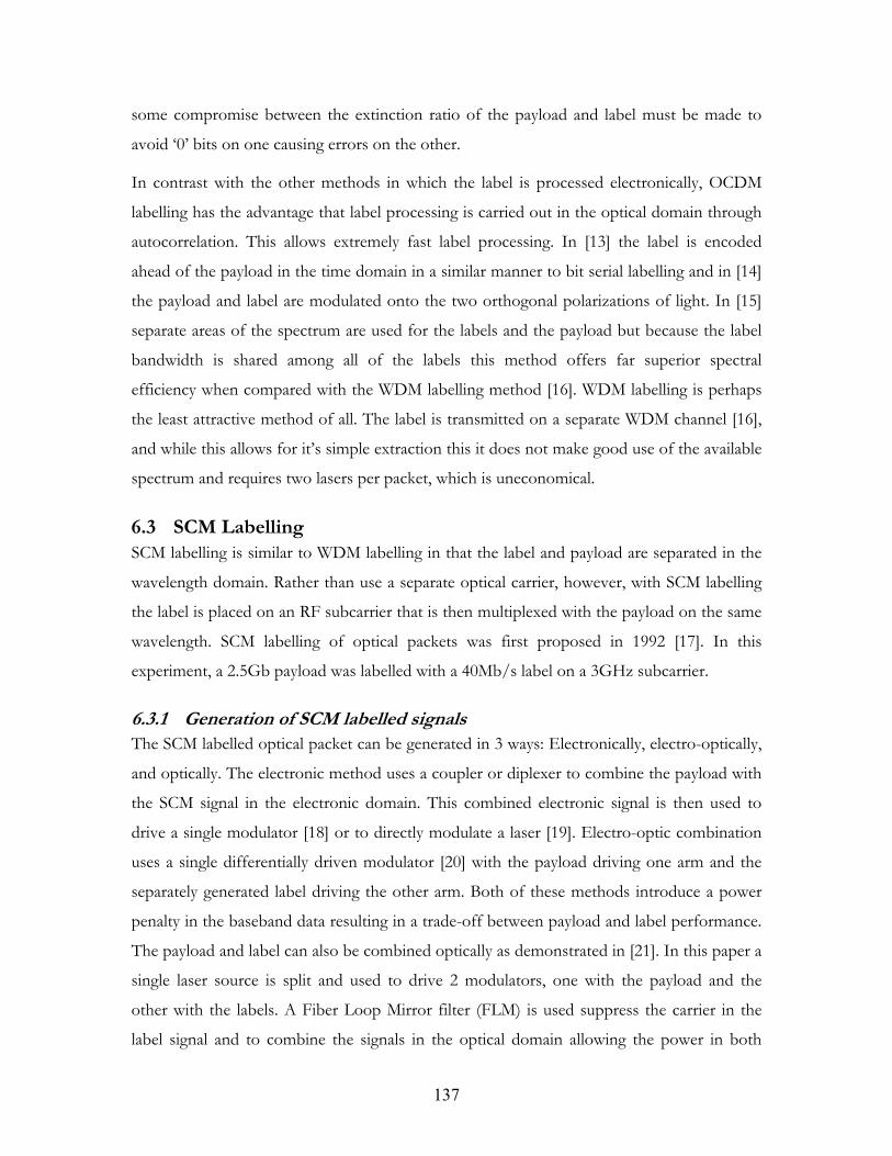
137
some compromise between the extinction ratio of the payload and label must be made to
avoid ‘0’ bits on one causing errors on the other.
In contrast with the other methods in which the label is processed electronically, OCDM
labelling has the advantage that label processing is carried out in the optical domain through
autocorrelation. This allows extremely fast label processing. In [13] the label is encoded
ahead of the payload in the time domain in a similar manner to bit serial labelling and in [14]
the payload and label are modulated onto the two orthogonal polarizations of light. In [15]
separate areas of the spectrum are used for the labels and the payload but because the label
bandwidth is shared among all of the labels this method offers far superior spectral
efficiency when compared with the WDM labelling method [16]. WDM labelling is perhaps
the least attractive method of all. The label is transmitted on a separate WDM channel [16],
and while this allows for it’s simple extraction this it does not make good use of the available
spectrum and requires two lasers per packet, which is uneconomical.
6.3 SCM Labelling SCM labelling is similar to WDM labelling in that the label and payload are separated in the
wavelength domain. Rather than use a separate optical carrier, however, with SCM labelling
the label is placed on an RF subcarrier that is then multiplexed with the payload on the same
wavelength. SCM labelling of optical packets was first proposed in 1992 [17]. In this
experiment, a 2.5Gb payload was labelled with a 40Mb/s label on a 3GHz subcarrier.
6.3.1 Generation of SCM labelled signals The SCM labelled optical packet can be generated in 3 ways: Electronically, electro-optically,
and optically. The electronic method uses a coupler or diplexer to combine the payload with
the SCM signal in the electronic domain. This combined electronic signal is then used to
drive a single modulator [18] or to directly modulate a laser [19]. Electro-optic combination
uses a single differentially driven modulator [20] with the payload driving one arm and the
separately generated label driving the other arm. Both of these methods introduce a power
penalty in the baseband data resulting in a trade-off between payload and label performance.
The payload and label can also be combined optically as demonstrated in [21]. In this paper a
single laser source is split and used to drive 2 modulators, one with the payload and the
other with the labels. A Fiber Loop Mirror filter (FLM) is used suppress the carrier in the
label signal and to combine the signals in the optical domain allowing the power in both
138
label and payload to be maximized without affecting the other. The disadvantage of this
technique is that it is bulky and requires two modulators.
Generally, the labels are placed at a subcarrier frequency which is equal to or higher than the
clock frequency of the payload signal. To improve the spectral efficiency, an in-band SCM
technique was presented in [22]. This method uses a combination of orthogonal and SCM
labelling. A 40Gb/s DPSK payload was combined with 3GHz subcarrier labels at 25Mb/s.
A major advantage of this technique is that the RF components required to generate 3GHz
subcarriers are much less costly than those required for 40GHz or beyond. However the
system is more complicated due to the coherent detection required and the need for two
modulators in the transmitter.
6.3.2 OCSS One form of SCM labelling is known as optical carrier suppression and separation (OCSS)
[23]. Here, a sine wave RF clock and its inverse are used to drive a differential modulator
with a CW input. The resulting spectrum consists of two subcarriers spaced by twice the RF
clock frequency with the optical carrier suppressed between them. The two modes can then
be filtered and modulated independently, one with the payload and the other with the label.
Good extinction and low crosstalk make this method attractive but the main problems with
method are the complicated transmitter and node design that require three modulators in the
transmitter and two in every node.
6.3.3 Reading SCM labels An SCM label can be read by direct detection of the entire optical channel, and then
downconversion using the RF carrier [17]. Downconversion is not ideal because it requires
additional high frequency components. In addition RF fading caused by double sidebands
experiencing different phase shifts due to fiber dispersion occurs [24]. An alternative method
[25], allows direct detection of the labels. Providing that the subcarriers are Amplitude Shift
Keyed (ASK), they can be optically band pass filtered and detected directly, because the filter
blocks the energy from the other optical carriers and subcarriers with the effect that the
photodiode appears to be illuminated by a single intensity modulated signal. This technique
removes the need for high frequency components and additionally overcomes the fading
problem [26,27]. The fading problem has also been overcome using a more complex

139
modulation technique to give single sideband (SSB) SCM [28] which also allows for greater
spectral efficiency but is more complex to generate.
6.3.4 Swapping Once the label and payload have been separated it is relatively simple to swap the labels with
new ones if required. A modulator in the node, driven with the subcarrier data only will add
the new labels to the existing payload prior to retransmission. A sub-optimal extinction ratio
is required however to ensure that light is always present to modulate onto.
6.3.5 Advantages of SCM Labelling The advantages that SCM labelling offer over other forms include:
1. Simple bookkeeping since the same wavelength channel is used for the payload and
label. This is in contrast to WDM labelling systems, and systems which use dedicated
bandwidth for labelling.
2. In contrast to bit serial labelling in which tight timing and synchronization is
required, with SCM the label and payload arrive together in time but can be
processed asynchronously. This greatly simplifies the node architectures.
3. Label extraction is very simple, requiring only optical filters, and label swapping is
also easily available.
6.3.6 Disadvantages of SCM Labelling 1. The RF fading problem discussed previously is a potential disadvantage of SCM
labelling but it can be easily overcome using filtration and direct detection, or SSB
modulation.
2. Poor spectral efficiency is achieved when using an out of band subcarrier, however
as we show in the next section, the use of the data clock as the RF subcarrier results
in good spectral efficiency. In addition, advanced modulation formats can be used to
narrow the spectrum further. Finally, in-band SCM labelling has also been
demonstrated.
3. Nonlinearities due to imperfect components can cause Inter-Modulation Distortion
(IMD) between adjacent labels leading to the creation of spectral components which
may lie under and interfere with the payload.
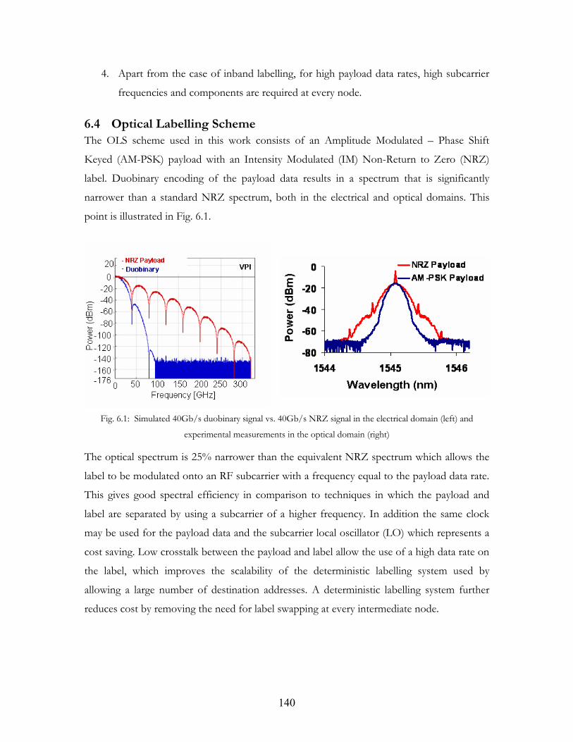
140
4. Apart from the case of inband labelling, for high payload data rates, high subcarrier
frequencies and components are required at every node.
6.4 Optical Labelling Scheme The OLS scheme used in this work consists of an Amplitude Modulated – Phase Shift
Keyed (AM-PSK) payload with an Intensity Modulated (IM) Non-Return to Zero (NRZ)
label. Duobinary encoding of the payload data results in a spectrum that is significantly
narrower than a standard NRZ spectrum, both in the electrical and optical domains. This
point is illustrated in Fig. 6.1.
Fig. 6.1: Simulated 40Gb/s duobinary signal vs. 40Gb/s NRZ signal in the electrical domain (left) and
experimental measurements in the optical domain (right)
The optical spectrum is 25% narrower than the equivalent NRZ spectrum which allows the
label to be modulated onto an RF subcarrier with a frequency equal to the payload data rate.
This gives good spectral efficiency in comparison to techniques in which the payload and
label are separated by using a subcarrier of a higher frequency. In addition the same clock
may be used for the payload data and the subcarrier local oscillator (LO) which represents a
cost saving. Low crosstalk between the payload and label allow the use of a high data rate on
the label, which improves the scalability of the deterministic labelling system used by
allowing a large number of destination addresses. A deterministic labelling system further
reduces cost by removing the need for label swapping at every intermediate node.
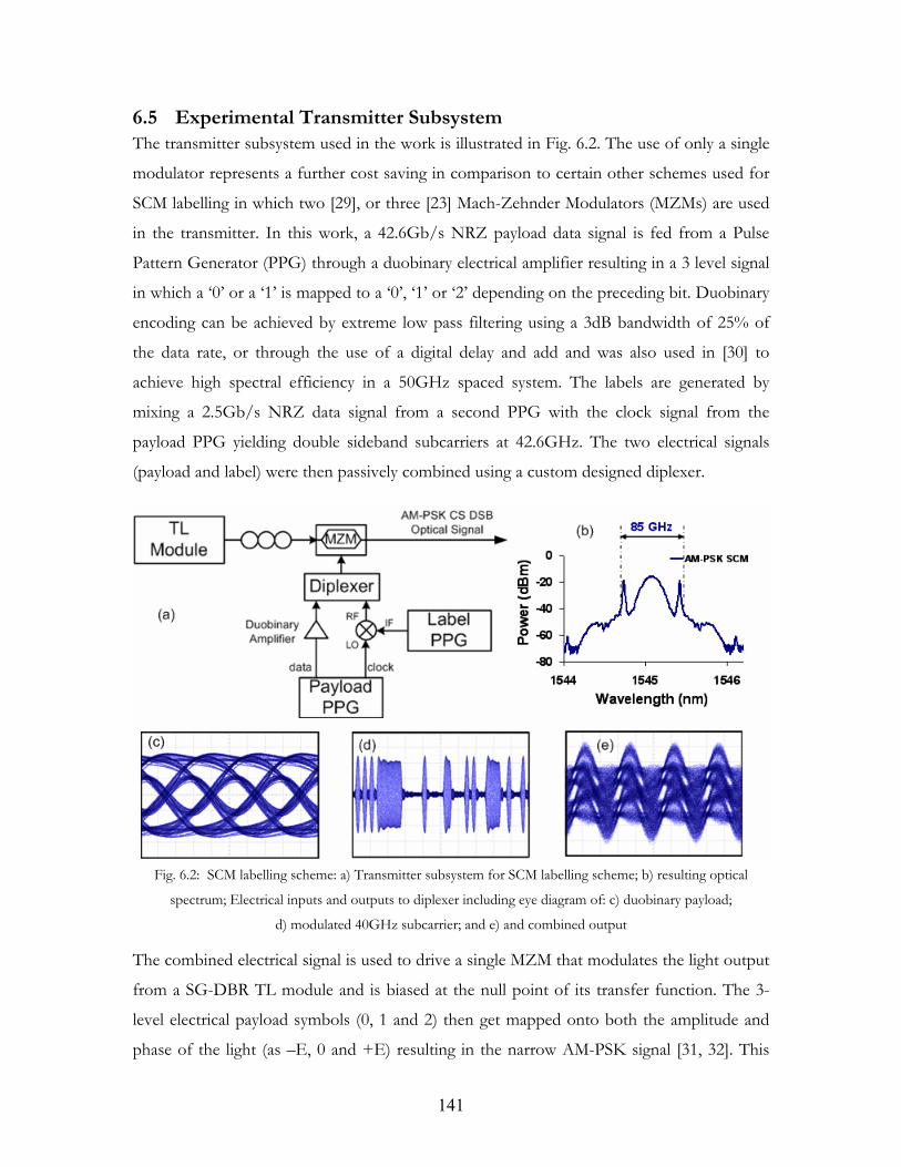
141
6.5 Experimental Transmitter Subsystem The transmitter subsystem used in the work is illustrated in Fig. 6.2. The use of only a single
modulator represents a further cost saving in comparison to certain other schemes used for
SCM labelling in which two [29], or three [23] Mach-Zehnder Modulators (MZMs) are used
in the transmitter. In this work, a 42.6Gb/s NRZ payload data signal is fed from a Pulse
Pattern Generator (PPG) through a duobinary electrical amplifier resulting in a 3 level signal
in which a ‘0’ or a ‘1’ is mapped to a ‘0’, ‘1’ or ‘2’ depending on the preceding bit. Duobinary
encoding can be achieved by extreme low pass filtering using a 3dB bandwidth of 25% of
the data rate, or through the use of a digital delay and add and was also used in [30] to
achieve high spectral efficiency in a 50GHz spaced system. The labels are generated by
mixing a 2.5Gb/s NRZ data signal from a second PPG with the clock signal from the
payload PPG yielding double sideband subcarriers at 42.6GHz. The two electrical signals
(payload and label) were then passively combined using a custom designed diplexer.
Fig. 6.2: SCM labelling scheme: a) Transmitter subsystem for SCM labelling scheme; b) resulting optical
spectrum; Electrical inputs and outputs to diplexer including eye diagram of: c) duobinary payload;
d) modulated 40GHz subcarrier; and e) and combined output
The combined electrical signal is used to drive a single MZM that modulates the light output
from a SG-DBR TL module and is biased at the null point of its transfer function. The 3-
level electrical payload symbols (0, 1 and 2) then get mapped onto both the amplitude and
phase of the light (as –E, 0 and +E) resulting in the narrow AM-PSK signal [31, 32]. This
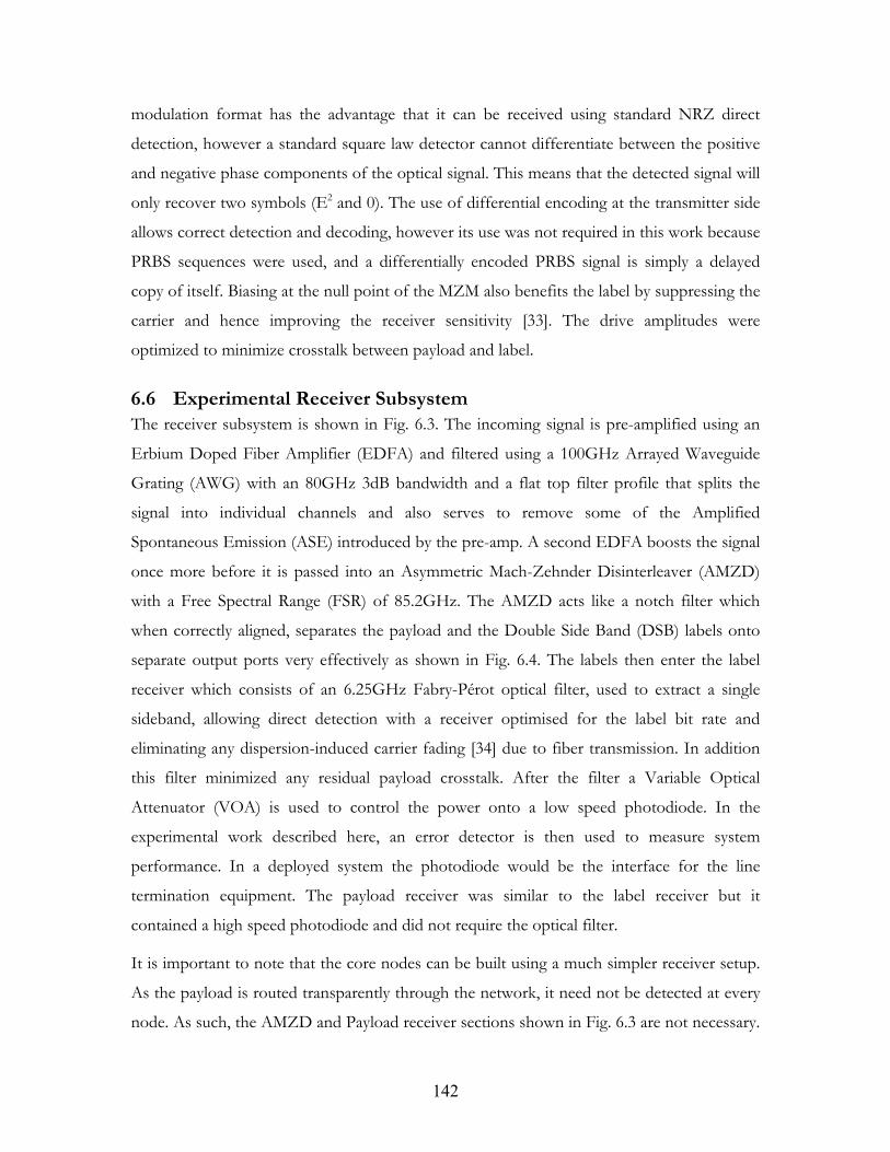
142
modulation format has the advantage that it can be received using standard NRZ direct
detection, however a standard square law detector cannot differentiate between the positive
and negative phase components of the optical signal. This means that the detected signal will
only recover two symbols (E2 and 0). The use of differential encoding at the transmitter side
allows correct detection and decoding, however its use was not required in this work because
PRBS sequences were used, and a differentially encoded PRBS signal is simply a delayed
copy of itself. Biasing at the null point of the MZM also benefits the label by suppressing the
carrier and hence improving the receiver sensitivity [33]. The drive amplitudes were
optimized to minimize crosstalk between payload and label.
6.6 Experimental Receiver Subsystem The receiver subsystem is shown in Fig. 6.3. The incoming signal is pre-amplified using an
Erbium Doped Fiber Amplifier (EDFA) and filtered using a 100GHz Arrayed Waveguide
Grating (AWG) with an 80GHz 3dB bandwidth and a flat top filter profile that splits the
signal into individual channels and also serves to remove some of the Amplified
Spontaneous Emission (ASE) introduced by the pre-amp. A second EDFA boosts the signal
once more before it is passed into an Asymmetric Mach-Zehnder Disinterleaver (AMZD)
with a Free Spectral Range (FSR) of 85.2GHz. The AMZD acts like a notch filter which
when correctly aligned, separates the payload and the Double Side Band (DSB) labels onto
separate output ports very effectively as shown in Fig. 6.4. The labels then enter the label
receiver which consists of an 6.25GHz Fabry-Pérot optical filter, used to extract a single
sideband, allowing direct detection with a receiver optimised for the label bit rate and
eliminating any dispersion-induced carrier fading [34] due to fiber transmission. In addition
this filter minimized any residual payload crosstalk. After the filter a Variable Optical
Attenuator (VOA) is used to control the power onto a low speed photodiode. In the
experimental work described here, an error detector is then used to measure system
performance. In a deployed system the photodiode would be the interface for the line
termination equipment. The payload receiver was similar to the label receiver but it
contained a high speed photodiode and did not require the optical filter.
It is important to note that the core nodes can be built using a much simpler receiver setup.
As the payload is routed transparently through the network, it need not be detected at every
node. As such, the AMZD and Payload receiver sections shown in Fig. 6.3 are not necessary.
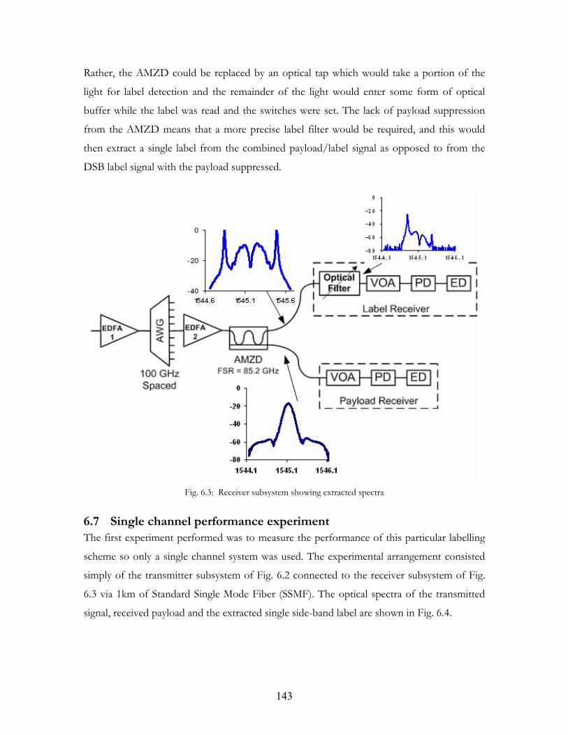
143
Rather, the AMZD could be replaced by an optical tap which would take a portion of the
light for label detection and the remainder of the light would enter some form of optical
buffer while the label was read and the switches were set. The lack of payload suppression
from the AMZD means that a more precise label filter would be required, and this would
then extract a single label from the combined payload/label signal as opposed to from the
DSB label signal with the payload suppressed.
Fig. 6.3: Receiver subsystem showing extracted spectra
6.7 Single channel performance experiment The first experiment performed was to measure the performance of this particular labelling
scheme so only a single channel system was used. The experimental arrangement consisted
simply of the transmitter subsystem of Fig. 6.2 connected to the receiver subsystem of Fig.
6.3 via 1km of Standard Single Mode Fiber (SSMF). The optical spectra of the transmitted
signal, received payload and the extracted single side-band label are shown in Fig. 6.4.
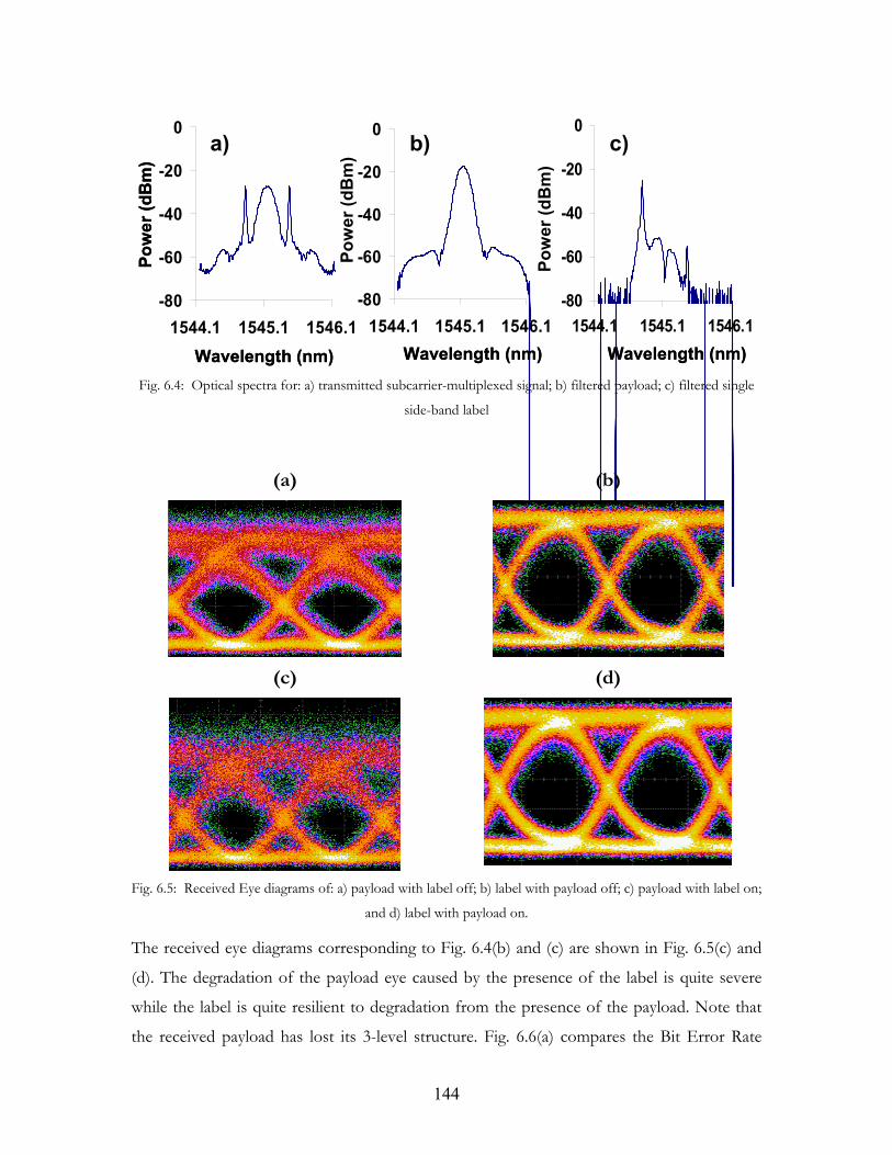
144
Wavelength (nm) Wavelength (nm)
Pow
er (d
Bm
)
-80
-60
-40
-20
0
1544.1 1545.1 1546.1-80
-60
-40
-20
0
1544.1 1545.1 1546.1-80
-60
-40
-20
0
1544.1 1545.1 1546.1
c)
Pow
er (d
Bm
)
Pow
er (d
Bm
)
Wavelength (nm)
b)a)
Wavelength (nm) Wavelength (nm)
Pow
er (d
Bm
)
-80
-60
-40
-20
0
1544.1 1545.1 1546.1-80
-60
-40
-20
0
1544.1 1545.1 1546.1-80
-60
-40
-20
0
1544.1 1545.1 1546.1
c)
Pow
er (d
Bm
)
Pow
er (d
Bm
)
Wavelength (nm)
b)a)
Fig. 6.4: Optical spectra for: a) transmitted subcarrier-multiplexed signal; b) filtered payload; c) filtered single
side-band label
(a)
(b)
(c)
(d)
Fig. 6.5: Received Eye diagrams of: a) payload with label off; b) label with payload off; c) payload with label on;
and d) label with payload on.
The received eye diagrams corresponding to Fig. 6.4(b) and (c) are shown in Fig. 6.5(c) and
(d). The degradation of the payload eye caused by the presence of the label is quite severe
while the label is quite resilient to degradation from the presence of the payload. Note that
the received payload has lost its 3-level structure. Fig. 6.6(a) compares the Bit Error Rate
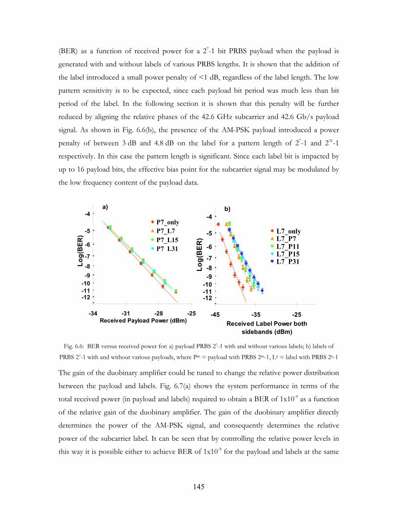
145
(BER) as a function of received power for a 27-1 bit PRBS payload when the payload is
generated with and without labels of various PRBS lengths. It is shown that the addition of
the label introduced a small power penalty of <1 dB, regardless of the label length. The low
pattern sensitivity is to be expected, since each payload bit period was much less than bit
period of the label. In the following section it is shown that this penalty will be further
reduced by aligning the relative phases of the 42.6 GHz subcarrier and 42.6 Gb/s payload
signal. As shown in Fig. 6.6(b), the presence of the AM-PSK payload introduced a power
penalty of between 3 dB and 4.8 dB on the label for a pattern length of 27-1 and 231-1
respectively. In this case the pattern length is significant. Since each label bit is impacted by
up to 16 payload bits, the effective bias point for the subcarrier signal may be modulated by
the low frequency content of the payload data.
-12-11-10
-9-8-7
-6
-5
-4
-45 -35 -25Received Label Power both
sidebands (dBm)
Log(
BER
)
L7_onlyL7_P7L7_P11L7_P15L7_P31
-4
-5
-6
-7-8-9
-10-11-12
-34 -31 -28 -25Received Payload Power (dBm)
Log(
BER
)
P7_onlyP7_L7P7_L15P7_L31
a) b)
-12-11-10
-9-8-7
-6
-5
-4
-45 -35 -25Received Label Power both
sidebands (dBm)
Log(
BER
)
L7_onlyL7_P7L7_P11L7_P15L7_P31
-4
-5
-6
-7-8-9
-10-11-12
-34 -31 -28 -25Received Payload Power (dBm)
Log(
BER
)
P7_onlyP7_L7P7_L15P7_L31
a) b)
Fig. 6.6: BER versus received power for: a) payload PRBS 27-1 with and without various labels; b) labels of
PRBS 27-1 with and without various payloads, where Pm = payload with PRBS 2m-1, Ln = label with PRBS 2n-1
The gain of the duobinary amplifier could be tuned to change the relative power distribution
between the payload and labels. Fig. 6.7(a) shows the system performance in terms of the
total received power (in payload and labels) required to obtain a BER of 1x10⁻⁹ as a function
of the relative gain of the duobinary amplifier. The gain of the duobinary amplifier directly
determines the power of the AM-PSK signal, and consequently determines the relative
power of the subcarrier label. It can be seen that by controlling the relative power levels in
this way it is possible either to achieve BER of 1x10⁻⁹ for the payload and labels at the same
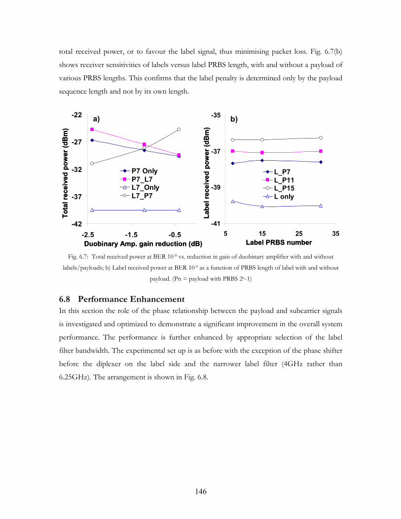
146
total received power, or to favour the label signal, thus minimising packet loss. Fig. 6.7(b)
shows receiver sensitivities of labels versus label PRBS length, with and without a payload of
various PRBS lengths. This confirms that the label penalty is determined only by the payload
sequence length and not by its own length.
-42
-37
-32
-27
-22
-2.5 -1.5 -0.5
P7 OnlyP7_L7L7_OnlyL7_P7
-41
-39
-37
-35
5 15 25 35
L_P7L_P11L_P15L only
Duobinary Amp. gain reduction (dB) Label PRBS number
Tota
l rec
eive
d po
wer
(dB
m)
Labe
l rec
eive
d po
wer
(dB
m)
a) b)
-42
-37
-32
-27
-22
-2.5 -1.5 -0.5
P7 OnlyP7_L7L7_OnlyL7_P7
-41
-39
-37
-35
5 15 25 35
L_P7L_P11L_P15L only
Duobinary Amp. gain reduction (dB) Label PRBS number
Tota
l rec
eive
d po
wer
(dB
m)
Labe
l rec
eive
d po
wer
(dB
m)
a) b)
Fig. 6.7: Total received power at BER 10-9 vs. reduction in gain of duobinary amplifier with and without
labels/payloads; b) Label received power at BER 10-9 as a function of PRBS length of label with and without
payload. (Pn = payload with PRBS 2n-1)
6.8 Performance Enhancement In this section the role of the phase relationship between the payload and subcarrier signals
is investigated and optimized to demonstrate a significant improvement in the overall system
performance. The performance is further enhanced by appropriate selection of the label
filter bandwidth. The experimental set up is as before with the exception of the phase shifter
before the diplexer on the label side and the narrower label filter (4GHz rather than
6.25GHz). The arrangement is shown in Fig. 6.8.
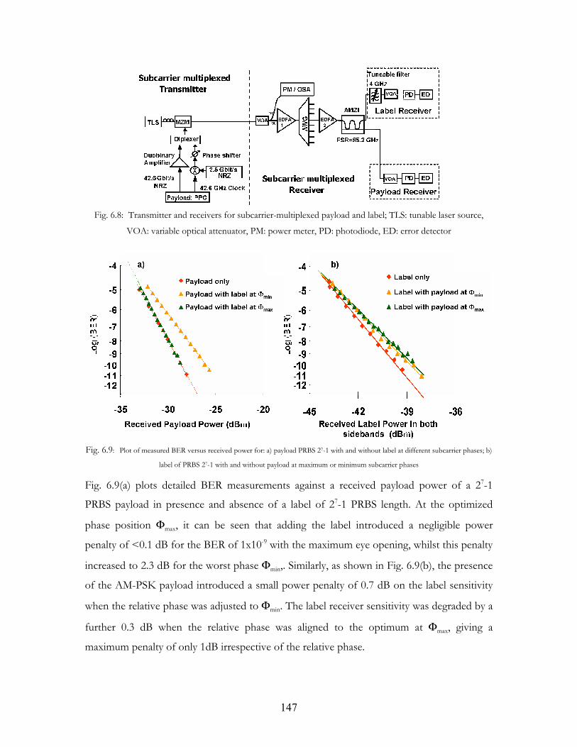
147
Fig. 6.8: Transmitter and receivers for subcarrier-multiplexed payload and label; TLS: tunable laser source,
VOA: variable optical attenuator, PM: power meter, PD: photodiode, ED: error detector
Fig. 6.9: Plot of measured BER versus received power for: a) payload PRBS 27-1 with and without label at different subcarrier phases; b)
label of PRBS 27-1 with and without payload at maximum or minimum subcarrier phases
Fig. 6.9(a) plots detailed BER measurements against a received payload power of a 27-1
PRBS payload in presence and absence of a label of 27-1 PRBS length. At the optimized
phase position Φmax, it can be seen that adding the label introduced a negligible power
penalty of <0.1 dB for the BER of 1x10⁻⁹ with the maximum eye opening, whilst this penalty
increased to 2.3 dB for the worst phase Φmin,. Similarly, as shown in Fig. 6.9(b), the presence
of the AM-PSK payload introduced a small power penalty of 0.7 dB on the label sensitivity
when the relative phase was adjusted to Φmin. The label receiver sensitivity was degraded by a
further 0.3 dB when the relative phase was aligned to the optimum at Φmax, giving a
maximum penalty of only 1dB irrespective of the relative phase.
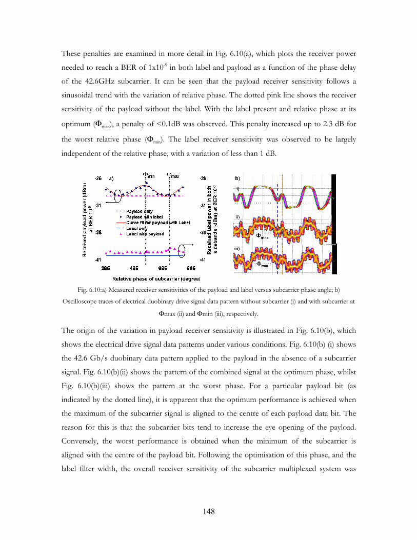
148
These penalties are examined in more detail in Fig. 6.10(a), which plots the receiver power
needed to reach a BER of 1x10⁻⁹ in both label and payload as a function of the phase delay
of the 42.6GHz subcarrier. It can be seen that the payload receiver sensitivity follows a
sinusoidal trend with the variation of relative phase. The dotted pink line shows the receiver
sensitivity of the payload without the label. With the label present and relative phase at its
optimum (Φmax), a penalty of <0.1dB was observed. This penalty increased up to 2.3 dB for
the worst relative phase (Φmin). The label receiver sensitivity was observed to be largely
independent of the relative phase, with a variation of less than 1 dB.
Fig. 6.10: a) Measured receiver sensitivities of the payload and label versus subcarrier phase angle; b)
Oscilloscope traces of electrical duobinary drive signal data pattern without subcarrier (i) and with subcarrier at
Φmax (ii) and Φmin (iii), respectively.
The origin of the variation in payload receiver sensitivity is illustrated in Fig. 6.10(b), which
shows the electrical drive signal data patterns under various conditions. Fig. 6.10(b) (i) shows
the 42.6 Gb/s duobinary data pattern applied to the payload in the absence of a subcarrier
signal. Fig. 6.10(b)(ii) shows the pattern of the combined signal at the optimum phase, whilst
Fig. 6.10(b)(iii) shows the pattern at the worst phase. For a particular payload bit (as
indicated by the dotted line), it is apparent that the optimum performance is achieved when
the maximum of the subcarrier signal is aligned to the centre of each payload data bit. The
reason for this is that the subcarrier bits tend to increase the eye opening of the payload.
Conversely, the worst performance is obtained when the minimum of the subcarrier is
aligned with the centre of the payload bit. Following the optimisation of this phase, and the
label filter width, the overall receiver sensitivity of the subcarrier multiplexed system was
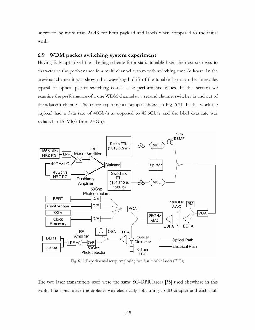
149
improved by more than 2.0dB for both payload and labels when compared to the initial
work.
6.9 WDM packet switching system experiment Having fully optimized the labelling scheme for a static tunable laser, the next step was to
characterize the performance in a multi-channel system with switching tunable lasers. In the
previous chapter it was shown that wavelength drift of the tunable lasers on the timescales
typical of optical packet switching could cause performance issues. In this section we
examine the performance of a one WDM channel as a second channel switches in and out of
the adjacent channel. The entire experimental setup is shown in Fig. 6.11. In this work the
payload had a data rate of 40Gb/s as opposed to 42.6Gb/s and the label data rate was
reduced to 155Mb/s from 2.5Gb/s.
Fig. 6.11: Experimental setup employing two fast tunable lasers (FTLs)
The two laser transmitters used were the same SG-DBR lasers [35] used elsewhere in this
work. The signal after the diplexer was electrically split using a 6dB coupler and each path
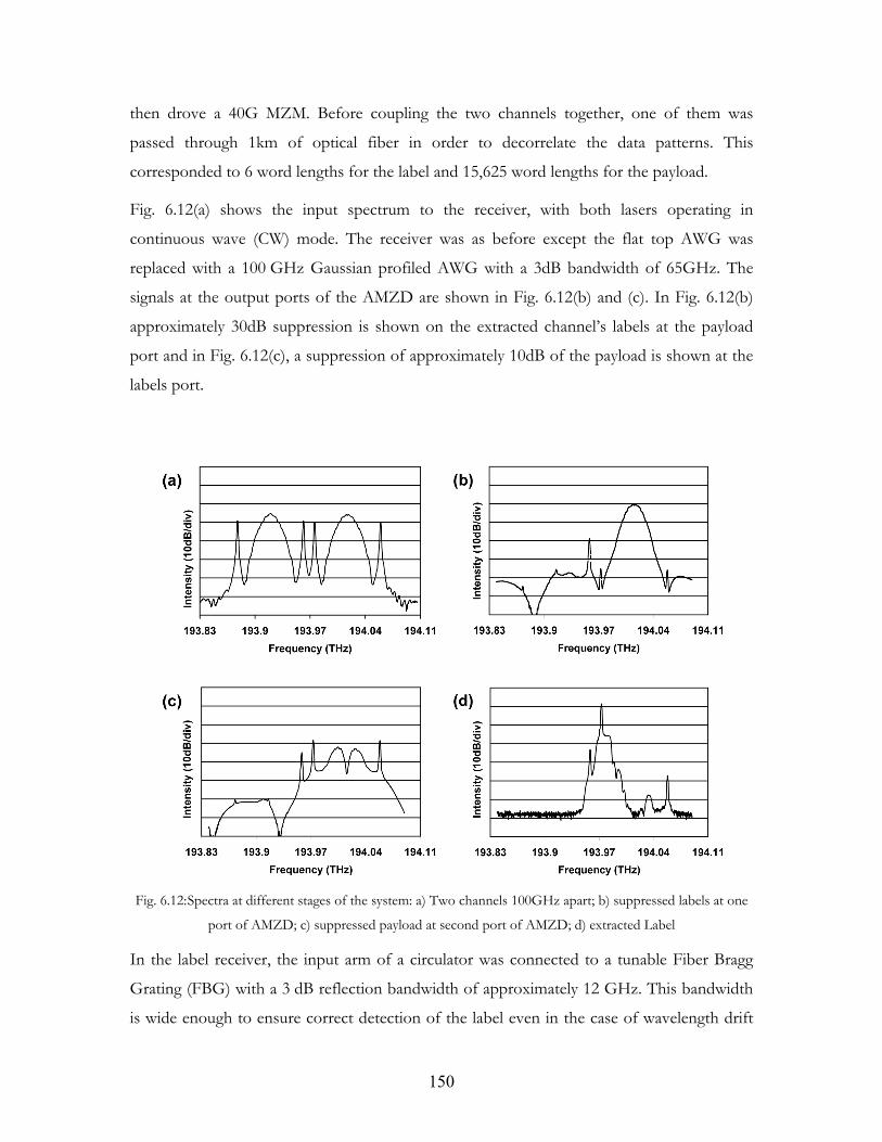
150
then drove a 40G MZM. Before coupling the two channels together, one of them was
passed through 1km of optical fiber in order to decorrelate the data patterns. This
corresponded to 6 word lengths for the label and 15,625 word lengths for the payload.
Fig. 6.12(a) shows the input spectrum to the receiver, with both lasers operating in
continuous wave (CW) mode. The receiver was as before except the flat top AWG was
replaced with a 100 GHz Gaussian profiled AWG with a 3dB bandwidth of 65GHz. The
signals at the output ports of the AMZD are shown in Fig. 6.12(b) and (c). In Fig. 6.12(b)
approximately 30dB suppression is shown on the extracted channel’s labels at the payload
port and in Fig. 6.12(c), a suppression of approximately 10dB of the payload is shown at the
labels port.
Fig. 6.12: Spectra at different stages of the system: a) Two channels 100GHz apart; b) suppressed labels at one
port of AMZD; c) suppressed payload at second port of AMZD; d) extracted Label
In the label receiver, the input arm of a circulator was connected to a tunable Fiber Bragg
Grating (FBG) with a 3 dB reflection bandwidth of approximately 12 GHz. This bandwidth
is wide enough to ensure correct detection of the label even in the case of wavelength drift
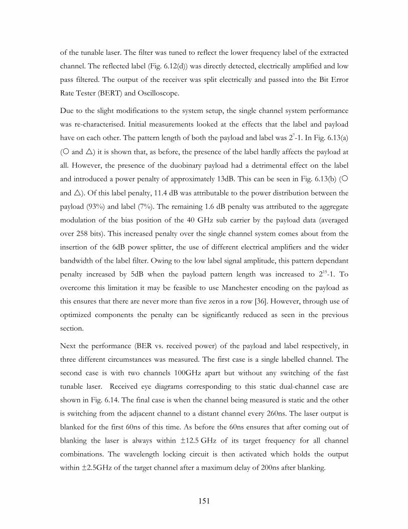
151
of the tunable laser. The filter was tuned to reflect the lower frequency label of the extracted
channel. The reflected label (Fig. 6.12(d)) was directly detected, electrically amplified and low
pass filtered. The output of the receiver was split electrically and passed into the Bit Error
Rate Tester (BERT) and Oscilloscope.
Due to the slight modifications to the system setup, the single channel system performance
was re-characterised. Initial measurements looked at the effects that the label and payload
have on each other. The pattern length of both the payload and label was 27-1. In Fig. 6.13(a)
( and ) it is shown that, as before, the presence of the label hardly affects the payload at
all. However, the presence of the duobinary payload had a detrimental effect on the label
and introduced a power penalty of approximately 13dB. This can be seen in Fig. 6.13(b) (
and ). Of this label penalty, 11.4 dB was attributable to the power distribution between the
payload (93%) and label (7%). The remaining 1.6 dB penalty was attributed to the aggregate
modulation of the bias position of the 40 GHz sub carrier by the payload data (averaged
over 258 bits). This increased penalty over the single channel system comes about from the
insertion of the 6dB power splitter, the use of different electrical amplifiers and the wider
bandwidth of the label filter. Owing to the low label signal amplitude, this pattern dependant
penalty increased by 5dB when the payload pattern length was increased to 215-1. To
overcome this limitation it may be feasible to use Manchester encoding on the payload as
this ensures that there are never more than five zeros in a row [36]. However, through use of
optimized components the penalty can be significantly reduced as seen in the previous
section.
Next the performance (BER vs. received power) of the payload and label respectively, in
three different circumstances was measured. The first case is a single labelled channel. The
second case is with two channels 100GHz apart but without any switching of the fast
tunable laser. Received eye diagrams corresponding to this static dual-channel case are
shown in Fig. 6.14. The final case is when the channel being measured is static and the other
is switching from the adjacent channel to a distant channel every 260ns. The laser output is
blanked for the first 60ns of this time. As before the 60ns ensures that after coming out of
blanking the laser is always within ±12.5 GHz of its target frequency for all channel
combinations. The wavelength locking circuit is then activated which holds the output
within ±2.5GHz of the target channel after a maximum delay of 200ns after blanking.
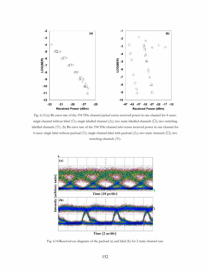
152
Fig. 6.13: (a) Bit error rate of the 194 THz channel payload versus received power in one channel for 4 cases:
single channel without label ( ); single labelled channel ( ); two static labelled channels ( ); two switching
labelled channels ( ). (b) Bit error rate of the 194 THz channel label versus received power in one channel for
4 cases: single label without payload ( ); single channel label with payload ( ); two static channels ( ); two
switching channels ( ).
Fig. 6.14: Received eye diagrams of the payload (a) and label (b) for 2 static channel case
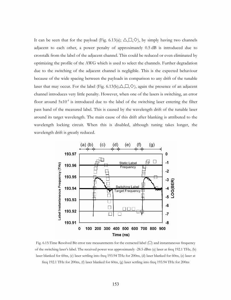
153
It can be seen that for the payload (Fig. 6.13(a); , , ), by simply having two channels
adjacent to each other, a power penalty of approximately 0.5 dB is introduced due to
crosstalk from the label of the adjacent channel. This could be reduced or even eliminated by
optimizing the profile of the AWG which is used to select the channels. Further degradation
due to the switching of the adjacent channel is negligible. This is the expected behaviour
because of the wide spacing between the payloads in comparison to any drift of the tunable
laser that may occur. For the label (Fig. 6.13(b); , , ), again the presence of an adjacent
channel introduces very little penalty. However, when one of the lasers is switching, an error
floor around 5x10⁻⁴ is introduced due to the label of the switching laser entering the filter
pass band of the measured label. This is caused by the wavelength drift of the tunable laser
around its target wavelength. The main cause of this drift after blanking is attributed to the
wavelength locking circuit. When this is disabled, although tuning takes longer, the
wavelength drift is greatly reduced.
Fig. 6.15: Time Resolved Bit error rate measurements for the extracted label ( ) and instantaneous frequency
of the switching laser’s label. The received power was approximately -28.5 dBm (a) laser at freq 192.1 THz, (b)
laser blanked for 60ns, (c) laser settling into freq 193.94 THz for 200ns, (d) laser blanked for 60ns, (e) laser at
freq 192.1 THz for 200ns, (f) laser blanked for 60ns, (g) laser settling into freq 193.94 THz for 200ns

154
This effect is further illustrated in Fig. 6.15, which shows time resolved bit error rate
measurements with a received power of -28.5 dBm along with the instantaneous frequency
of the label of the switching laser. The instantaneous frequency was extracted from
complimentary outputs of the 85GHz AMZD biased at quadrature for the target frequency
by using the measured frequency response of the AMZD to resolve the laser output
frequency. The gating interval used for the time resolved BER measurements was 8ns and
this gating window could be stepped across the signal with a maximum resolution of 500ps..
The time in the plot is divided into 7 sections labelled (a) to (g).
1) During time (a) the switching laser is at the distant channel hence no errors
are observed in the measured label and no instantaneous frequency is
present.
2) During time (b) the switching laser has switched to the channel adjacent to
the measured channel but it is blanked for 60ns so again, no errors are
observed.
3) During time (c) the laser comes out of blanking, hence there are now two
adjacent labels, one at the frequency marked “static label frequency” and the
other settling into the frequency marked “switching label target frequency”.
It can be seen that during this time, the instantaneous frequency of the
switching label comes within 10GHz of the measured label and accordingly,
a burst of errors are seen during this time with the error rate at its worst
when the two labels are closest together and then reducing as the switching
laser settles into it’s target frequency.
4) During time (d) the laser is laser has switched to the distant channel again
and is blanked for another 60ns and no errors are seen.
5) During times (e) the laser comes out of blanking on the distant channel and
the errors seen on the label during this time are caused by its own payload.
6) During times (f) and (g) the cycle is repeated once again.
It can clearly be seen that the switching events in the tunable laser correspond to the time
intervals when there are significant errors on the received label data. While the laser is
blanked and also while it sits at the distant channel, the error rate of the measured channel
155
drops considerably. However as the laser tunes towards and begins settling on the 193.94
THz channel the error rate increases dramatically.
6.10 Conclusions This chapter described the development of transmitter and receiver subsystems for a label
switched OPS system. The transmitter was based on a fast tunable SG-DBR laser module
and work was carried out that explored the system effects of the wavelength drift of lasers,
which had been characterised in the previous chapter.
A number of OLS schemes and methods were described in the early part of the chapter with
the focus then turning to the particular labelling method used in this work, SCM labelling.
Some of the literature on this topic was then reviewed before the experimental work was
described. Three experiments were detailed: The first was the basic design and
characterisation of label switching scheme which aside from the common benefits of SCM
labels, also offers good spectral efficiency with low payload/label crosstalk. The second set
of experiments involved further refinement and improvement of the transmission
characteristics of the labelling method by optimization of the amplitude and phase of the
label and payload relative to each other. The third experiment expanded the work from a
single static channel to a two channel dynamic system. To date, much of the literature on
OLS has looked primarily at static single channel systems. Work has focused on the labelling
techniques and schemes but the use of these schemes in a system employing multiple
switching channels has been somewhat neglected. Error free transmission for both payload
and label in a static dual-channel system with 0.4b/s/Hz spectral efficiency was achieved.
However, it was shown that in WDM systems when the lasers employed in the transmitters
were switching, the labels were severely impaired and a bit error floor was observed. By time
resolving the error measurements it was shown that this error floor corresponded to and was
due to the wavelength switching effects of the tunable lasers. Clearly, this interference must
be overcome to avoid routing errors and possible methods include increasing the blanking
time and/or channel spacing. However both of these solutions reduce network throughput.
More attractive solutions include optimised channel and label filter profiles, the use of single
side band subcarrier generation to eliminate interference between labels of adjacent channels,
and optimisation of the transient laser dynamics including operation of wavelength locking
technique during the existing blanking period.
156
References [1] X. Dai, L.N. Binh, Y.H. Ja, "Novel realtime time-division-multiplex optical packet
switching, using nonlinear effect," Optoelectronics [see also IEE Proceedings-Optoelectronics], IEE
Proceedings J , vol.137, no.3, pp.141-146, Jun 1990
[2] D.J Blumenthal, A. Carena, L. Rau, V. Curri, S. Humphries, "All-optical label
swapping with wavelength conversion for WDM-IP networks with subcarrier multiplexed
addressing," Photonics Technology Letters, IEEE , vol.11, no.11, pp.1497-1499, Nov 1999
[3] J. Capmany, D. Pastor, S. Sales, B. Ortega, 'Subcarrier Multiplexed Optical Labels
Swapping Based on Subcarrier Multiplexing: A Network Paradigm for the Implementation
of Optical Internet'. ICTON 2003
[4] S. J. B Yoo, 'Optical Label Switching, MPLS, MPLambdaS and GMPLS'. Optical
Networks Magazine, May/June 2003, p 17-31
[5] P. Pruncal, M. Santoro, T. R Fan, “Spread-spectrum fibre optic local area network
using optical processing” J Lighw. Technol., Vol LT-4, no. 5, pp 547-554, May 1986.
[6] P. Pruncal, D. J. Blumenthal, P. A. Perrier, “Photonic switch with optically self-
routed bit switching”, IEEE Commun. Mag. Vol 25, no 5., pp 50-55, May 1987
[7] W. L. Ha, R. M. Fortenberry, R. S. Tucker, ”Demonstration of photonic fast packet
switching at 700Mb/s data rate” Electron Lett, vol 27. no 10. pp 789 – 790., May 1991
[8] W. Wang, L. G. Rau, D. J Blumenthal, “160Gb/s variable length packet/10Gb/s
label all-optical label switching with wavelength conversion and unicast/multicast
operation”, J. Lightw. Technol., vol 23, no 1. pp 211 – 218, Jan 2005
[9] N Chi, et al, “Experimental Demonstration of cascaded transmission and all-optical
label swapping of orthogonal IM/FSK labelled signal”, Electron Lett. Vol 39, no. 8, pp 676-
678, Apr 2003
[10] N. Deng, Y. Yang, C.K Chan, W. Hung, L.K Chen, “Intensity Modulated Labelling
and all optical label swapping on angle-modulated packets”, IEEE Photon. Technol. Lett., vol
16. no 4, pp 1218 – 1220, Apr. 2004.
157
[11] N. Chi et al. Optical label swapping and packet transmission based on ASK/DPSK
orthogonal modulation format in IP-over- WDM Networks, presented at the Optical Fiber
Communications Conf. (OFC 2003), Atlanta, GA, Paper FS2.
[12] C. Chow and H. K. Tsang, Optical packet label using polarization shift keying
(PolSK) label and amplitude shift keying (ASK) payload, presented at Optical Fiber
Communications Conf. (OFC 2005), Anaheim, CA, Paper OME73.
[13] W.-H. Yang; C.-S. Wu, "Optical CDMA Label Encoding for Optical Packet
Switching in All-Optical Networks," Networks, 2006. ICON '06. 14th IEEE International
Conference on , vol.2, no., pp.1-5, Sept. 2006
[14] D.-Z. Hsu, "A novel photonic label switching based on optical code division
multiplexing," Telecommunications, 2003. ICT 2003. 10th International Conference on , vol.1, no.,
pp. 634-640 vol.1, 23 Feb.-1 March 2003
[15] A. Teixeira, P. Andre, P. Monteiro, M. Lima, R. Nogucira, and J. da Rocha, “All-
optical routing based on OCDMA headers,” in Proc. 16th Annual Meeting IEEE LEOS,
2003, vol. 2, pp. 1046–1047.
[16] S.-C. Lee, R. Varrazza, I.B. Djordjevic, S. Yu, "Optical label detection and packet
switching using a 4/spl times/4 optical crosspoint switch matrix," Optical Fiber Communication
Conference, 2004. OFC 2004 , vol.1, no., pp.-, 23-27 Feb. 2004
[17] A. Budman, E. Eichen, J. Schlafer, R. Olshansky, F. McAleavy, ”Multigigabit Optical
Packet Switch for self-routing networks with subcarrier addressing”, in Proc. Optical Fiber
Commun. Conf. (OFC 1992), San Jose, CA, USA, Feb. 1992, paper TUO4.
[18] M. Jeon, Z. Pan, J. Cao, S.J.B. Yoo, "All-optical sub-carrier label swapping with 2R
regeneration," Optical Fiber Communications Conference, 2003. OFC 2003 , vol., no., pp. 277-279
vol.1, 23-28 March 2003
[19] E. Park, A.E. Willner, "Network demonstration of self-routing wavelength packets
using an all-optical wavelength shifter and QPSK subcarrier routing control," Optical Fiber
Communications, 1996. OFC '96 , vol., no., pp. 114-115, 25 Feb.-1 March 1996
158
[20] R. Gaudino; D.J. Blumenthal, "A novel transmitter architecture for combined
baseband data and subcarrier-multiplexed control links using differential Mach-Zehnder
external modulators," Photonics Technology Letters, IEEE , vol.9, no.10, pp.1397-1399, Oct.
1997
[21] T. Dimmick, R. Doshi, R. Rajaduray, D. Blumenthal, '”Optically Multiplexed
Transmitter for hybrid baseband and subcarrier multiplexed signals”. European Conference on
Optical Communications (ECOC ‘00), 2000
[22] T. Flarup, C. Peucheret, J. J. V. Olmos, Y. Geng, J. Zhang, I. T. Monroy, P.
Jeppesen, 'Labeling of 40Gb/s DPSK Payload using In-Band Subcarrier Multiplexing'. Proc.
Optical Fiber Communications Conference (OFC) 2005, Vol. 3 p 3
[23] G.-K. Chang; J. Yu; A. Chowdhury, Y.-K. Yeo, "Optical carrier suppression and
separation label-switching techniques," Lightwave Technology, Journal of , vol.23, no.10, pp.
3372-3387, Oct. 2005
[24] G.H. Smith, D. Novak, "Broad-band millimeter-wave (38 GHz) fiber-wireless
transmission system using electrical and optical SSB modulation to overcome dispersion
effects," Photonics Technology Letters, IEEE , vol.10, no.1, pp.141-143, Jan 1998
[25] P.A. Greenhalgh, R.D. Abel, P.A. Davies, "Optical prefiltering in subcarrier
systems," Electronics Letters , vol.28, no.19, pp.1850-1852, 10 Sept. 1992
[26] M. Popov, A. Martinez, J. Capmany, D. Pastor, P.-Y. Fonjallaz, B. Ortega, "Fiber-
Bragg-grating-based device for payload and label separation in highly packed subcarrier-
multiplexed optical label swapping," Photonics Technology Letters, IEEE , vol.17, no.11, pp.
2445-2447, Nov. 2005
[27] H.-J. Lee; S.J.B. Yoo, V.K. Tsui, S.K.H Fong, "A simple all-optical label detection
and swapping technique incorporating a fiber Bragg grating filter," Photonics Technology Letters,
IEEE , vol.13, no.6, pp.635-637, Jun 2001
[28] Y.M. Lin, W.I. Way, G.K. Chang, "A novel optical label swapping technique using
erasable optical single-sideband subcarrier label," Photonics Technology Letters, IEEE , vol.12,
no.8, pp.1088-1090, Aug 2000
159
[29] N. Chi, J. Zhang and P. Jeppesen, “All-optical subcarrier labeling based on the
carrier suppression of the payload,” IEEE Photonics Technol. Lett., vol.15, pp. 781-783, May
2003.
[30] M. Deulk, J. Gripp, J. Simsarian, A. Bhardwaj, P. Bernasconi, M. Zirngibl, and O.
Laznicka, “Fast packet routing in a 2.5 Tb/s optical switch fabric with 40 Gb/s duobinary
signals at 0.8 b/s/Hz spectral efficiency” in Proc. Optical Fiber Commun. Conf. (OFC 2003) ,
Georgia, Mar. 2003, vol. 3, postdeadline paper PD8-1-3.
[31] P. J. Winzer and R.-J. Essiambre, “Advanced modulation formats for high-capacity
optical transport networks,” J. Lightw. Technol., vol. 24, pp. 4711-4728, Dec. 2006
[32] G. Charlet, “Progress in optical modulation formats for high-bit rate WDM
transmissions,” IEEE J. Sel. Topics Quant. Electron., vol. 12, pp. 469-483, Jul./Aug. 2006.
[33] R. Hui, B. Zhu, R. Huang, C. T. Allen, K. R. Demarest, D. Richards, “Subcarrier
multiplexing for high-speed optical transmission,” J. Lightw. Technol.,vol. 20, pp. 417-427,
Mar. 2002.
[34] GH. Smith, D. Novak, D., Z. Ahmed, ‘Overcoming chromatic dispersion effects in
fibre-wireless systems incorporating external modulators’, IEEE Trans. Microw. Theory
Tech., 1997, 45, pp. 1410–1415
[35] J. Buus, M.-C. Amann, D. J. Blumenthal, “Widely Tunable Monolithic Laser Diodes”
in Tunable Laser Diodes and Related Optical Sources, Wiley, New Jersey, 2005.
[36] J. Zhang, N. Chi, P. V. Holm-Nielsen, C. Peucheret, P. Jeppesen, “Performance of
Manchester-Coded Payload in an Optical FSK labelling scheme”. IEEE Photonics Technology
Letters, vol 15, pp 1174-1176, Aug 2003.
160
Chapter 7 – Discussion and Conclusion
Optical networks are constantly evolving; from single channel point to point Synchronous
Optical Network/Synchronous Digital Hierarchy (SONET/SDH) links, they have grown to
multi-channel Wavelength Division Multiplexed (WDM) networks carrying terabits of data
every second. Now, as the first true optical switching components are being deployed, the
next step in the evolution is from optical transport networks to optical switching networks.
In their earliest forms these networks will be somewhat analogous to early telephone
switching networks, in which a user will request some bandwidth, and a network manager
will meet the request by reconfiguring the network. Gradually, the majority of manual
intervention will be removed from the network as systems are put in place to enable
automatic self-reconfiguration in response to changing network conditions. The network will
recognise network faults or traffic congestion and automatically re-route high priority data
around them. The beginnings of this automated optical circuit switched network are already
being seen with the deployment of the Generalized Multi-Protocol Label Switching
(GMPLS) control plane as described in Chapter 2 of this thesis.
Optical Circuit Switching (OCS) is desirable for telecommunication carriers because it
provides significant cost saving without requiring a total overhaul of the network. Network
flexibility without the need to deploy personnel to each node site, and the removal of
Optical-Electrical-Optical (OEO) conversions in the node together represent a huge cost
saving. In addition these cost savings come without requiring a total overhaul of the
network. Current transport networks can be relatively easily upgraded to optical switching
networks with the replacement of electronic switching components in the node with their
optical counterparts.
In order to move to the next stage of in the evolutionary chain of optical networks however,
the capital investment may be much higher, and as such carriers will need to see a significant
cost saving or revenue gain before they will be willing to make that investment. While the
nodes in an OCS network simply switch data transparently without regard for its contents
optical burst and packet switching networks will route data transparently, meaning that nodes
will need to examine the data (or at least the label) passing through. In addition tunability is
161
required in the nodes raising the possibility that every laser transmitter in the network would
require replacement. The upgrade from OCS to Optical Burst Switching (OBS) or Optical
Packet Switching (OPS) ,therefore is not straightforward and certainly, if their current
network can provide the services they want to offer, then carriers will not invest simply
because the technology is available. Nevertheless, as component costs drop and the
technology matures it seems likely that OBS and OPS will be deployed in the network due to
the massive flexibility and efficiency that it offers. Indeed, OBS networks are already being
offered commercially for the access and metro spaces. The wide range of services that can be
offered by optical networks mean that it is quite possible that the network of the future will
consists of a combination of OCS, OBS and OPS all controlled by Optical Label Switching
(OLS).
At each stage of the evolution a whole host of new issues arise. Problems solved to enable
the previous stage of evolution often arise again in more complicated forms. The experience
and knowledge gained from the first time around is then built upon to come up with novel
solutions. An example of this would be dispersion management; now well understood for
point to point optical transport networks. However as optical switching emerges, and greater
connectivity between nodes is seen, dispersion management becomes a whole new problem
due to the diversity of paths that signals can travel to their destination. This thesis dealt
experimentally with a small fraction of the vast range of issues affecting future optical
switching networks.
The first two chapters provided background information regarding optical networks, WDM
and optical switching. While not intended to be a complete reference, the chapters and the
references therein were aimed to give the reader the knowledge required to understand the
motivation behind the experimental work and to provide a starting point for further reading
on topics of interest. Two of the most important sections of Chapter 2 dealt with the
primary switching techniques of interest in this work: OCS and OPS, however both sections
were dealt with quite differently. Because OCS, is for the most part a mature technology, at
least in terms of hardware and understanding, this section was concerned with higher level
topics such as the control plane and the applications enabled by OCS. In contrast, OPS is
still a long way from maturity and as such, its section discussed the possible implementations
of OPS, and the technological obstacles.
162
Chapters 3 – 5 were the experimental chapters and the three were similarly structured.
Detailed background information and a review of the literature on the topic was given
initially, followed by a description of the experiment, the results and some concluding
remarks. In all cases the actual numerical results obtained are specific to the system used in
the experiment. However, more important than these are the conclusions which are drawn
from these results and which apply to all similar systems.
Chapter 3 reported on experiments carried out to investigate the effect of channel
reconfiguration on network performance. A circulating loop based WDM testbed was used
for this work which involved measuring the transmission performance of channels as the
channel configuration changed and the network was then re-optimized for the new
configuration. The technique of Applied Constant Gain (ACG) was used to enable the study
of constant-gain based systems in a constant-power based circulating loop.
A number of issues were investigated including the performance of channels at different
launch powers, and with different dispersion maps. The main lesson learned from the work
however, is that wavelength dependent gain of the amplifiers results in a network
arrangement that is optimized for a certain channel configuration, but sub-optimal for
others. Reconfiguring the network therefore, can cause channel power divergence, which
may causing severe transmission penalties. In the worst case studied, the transmission reach
for the channel in question was reduced by nearly 1000km simply by changing the
wavelength of the other 4 channels in the configuration from a uniformly spread channel
configuration to a banded configuration. Clearly such penalties will have a considerable
impact on network throughput as transmission cannot begin until the network is re-
optimized for the new configuration, a process which can take anywhere from seconds to
minutes.
The set of experiments performed was intended to stimulate further study of these effects in
order that control mechanisms can be developed to avoid the penalties. An investigation of
different approaches to reconfiguration is required and one of the first tests would be to
return the system to a known state prior to reconfiguration. For example, in this work the
per channel attenuators were not adjusted prior to reconfiguration but if they were returned
to a known state (for example the fully loaded arrangement) it is possible that the effects of
gain error would be reduced. Another prospect for further work would be the development
163
of techniques which predict the response of the EDFA to a new channel configuration
based on the current configuration and known EDFA models. The system could then be
arranged using the predicted response during re-configuration and then fine tuned over time.
Furthermore, the gain error could be automatically accounted for with the use of dynamic
GEFs within the EDFA. A control circuit which monitored the wavelength dependent gain,
rather than the total gain would be required and this could feed back into the dynamic GEF
to keep the EDFA gain flat at all times. Finally, work should be carried out which
investigates the time resolved system performance as channels configurations are switched.
In such an experiment, transient EDFA gain effects will affect performance as well as steady
state effects.
Chapter 4 and 5 moved away from the relatively slow switching speeds typical of OCS and
toward the much faster form of optical switching: OPS. With wavelength switching taking
place so quickly in an OPS network, it is likely that the work from Chapter 3 would be
rendered redundant because the EDFAs would never reach a steady state; rather they would
experience constant gain transients.
In Chapter 4 fast tunable lasers were the subjects of the experiments. A novel tunable laser
design based on the slotted Fabry-Pérot (SFP) laser was shown to exhibit extremely fast
wavelength switching despite a very simple and inexpensive fabrication process. In most
commercially available fast tunable lasers the switching speed is limited by the spontaneous
carrier lifetime in the passive sections however all of the sections in these devices are active
and therefore switching times can be expected to be much faster. The devices are crudely
packaged and it is expected that the switching times measured are in fact limited by the drive
circuitry and crude packaging rather than by the devices themselves. These devices were fully
characterised and modulated with 10Gb/s data and it was shown that error free data
transmission was possible within a few nanoseconds. This indicates that devices based on
the SFP structure may be suitable for use in OPS systems.
Further advances in the design of the tunable SFPs have resulted in increased channel counts
and reduced channel spacing. Recently the SFP devices have been packaged in a high speed
butterfly package. Further work in this area would include the integration of such a device
into a system module employing control electronics and a lookup table which ensured
accurate and reliable wavelength switching between any of the available wavelengths. This
164
would allow the use of the devices in full systems-based experiments which are difficult
currently due to the crude packaging and control employed.
A commercially available SG-DBR laser was the subject of experiments detailed in chapters
4 and 5. Although the devices met their design specifications, initial work focussed on the
wavelength drift of these devices and the effect that it may have in an SCM labelled OPS
system. A wavelength drift of up to 7.5GHz was reported. In densely packed WDM systems
this level of wavelength drift can cause performance degradation. The drift can be improved
by increasing the blanking time or using more sophisticated wavelength lockers but the
disadvantages are reduced throughput and increase expense, respectively. Having
characterised the drift the TL was used in a novel SCM labelling scheme which offered
excellent spectral efficiency. The problem that the wavelength drift of the lasers can cause
was then investigated in a two channel system using the labelling technique. Severe
performance problems were observed which in a real system would cause incorrect routing
of packets.
Further work in this area would include the expansion of the WDM system from 2 lasers up
to 4 or 8 and to perform measurements while all of these lasers were switching between
channels concurrently, including the channel being measured. While significant errors were
seen with the measured laser in static mode it is expected that the performance would be
even worse when switching, due mainly to the static filters employed and the drift of the
lasers. In addition the labelling scheme could be developed to investigate single sideband
(SSB) operation or in band labelling. The technique could be modified to include label
swapping and in this case, a transmitter – node – receiver experiment could be designed.
The ongoing evolution of optical switching brings up new challenges and obstacles with
every new idea formed. The experiments reported in this thesis yielded important
conclusions, relevant to any researcher working in the areas studied and should stimulate
further investigation of the issues covered.

i
Appendix A – List of Publications
Refereed Journals
1) F. Smyth, E. Connolly, A.K. Mishra, A.D. Ellis, D. Cotter, A. Kaszubowska, L.P.
Barry, "Effects of Crosstalk in WDM Optical Label Switching Networks Due to
Wavelength Switching of a Tunable Laser," IEEE Photonics Technology Letters,
vol.18, no.20, pp.2177-2179, Oct. 2006
2) F. Smyth, E. Connolly, B. Roycroft, B. Corbett, P. Lambkin, L.P. Barry, "Fast
Wavelength Switching Lasers Using Two-Section Slotted Fabry-Pérot
Structures," IEEE Photonics Technology Letters, vol.18, no.20, pp.2105-2107, Oct.
2006
3) A.K. Mishra, A.D. Ellis, D. Cotter, F. Smyth, E. Connolly, L.P. Barry, "Spectrally
compact optical subcarrier multiplexing with 42.6 Gb/s AM-PSK payload and
2.5 Gb/s NRZ labels," Electronics Letters, vol.42, no.22, pp.1303-1304, Oct. 26
2006
4) E. Connolly, F. Smyth, A.K. Mishra, A. Kaszubowska-Anandarajah, L.P. Barry,
"Cross-Channel Interference Due to Wavelength Drift of Tunable Lasers in
DWDM Networks," IEEE Photonics Technology Letters, vol.19, no.8, pp.616-618,
April15, 2007
5) R. Phelan, W-H Guo, Q. Lu, D. Byrne, B. Roycroft, P. Lambkin, B. Corbett, F.
Smyth, L.P. Barry, B. Kelly, J. O'Gorman, J.F. Donegan, "A Novel Two-Section
Tunable Discrete Mode Fabry-Pérot Laser Exhibiting Nanosecond Wavelength
Switching," IEEE Journal of Quantum Electronics, vol.44, no.4, pp.331-337, April
2008
6) F. Smyth, D.C. Kilper, L.P. Barry, S. Chandrasekhar, “Applied Constant Gain
Amplification in Circulating Loop Experiments”, Submitted to IEEE Journal of
Lightwave Technology
ii
Reviewed Conferences
1) F. Smyth, L.P. Barry "Performance Issues in SCM label switched networks due
to tunable laser switching events", International Conference on Applications of Photonic
Technology (Photonics North 2006), pp 170, Quebec, 5-8 June 2006
2) G. Mulvihill, M. Ruffini, F. Smyth, L.P. Barry, L. Doyle, D. O'Mahony, "Optical
IP Switching a Solution to Dynamic Lightpath Establishment in Disaggregated
Network Architectures," International Conference on Transparent Optical Networks,
2006, vol.3, pp.78-81, June 2006
3) F. Smyth, B. Roycroft, B. Corbett, P. Lambkin, L.P. Barry, "Fast Wavelength
Switching Lasers Using Two-section Slotted FP Structures", European Conference
on Optical Communications (ECOC 2006), Paper We3.P.42 Cannes, France, 24 – 28
September 2006
4) A.K. Mishra, A.D. Ellis, D. Cotter, F. Smyth, E. Connolly, L.P. Barry, ‘Spectrally
Compact Optical Subcarrier Multiplexing for Label-Switched Networks with 42.6
Gb/s Duobinary Payload and 2.5Gb/s NRZ Labels’, European Conference on
Optical Communications (ECOC ‘06), Paper We2.4.4, Cannes, France, 24-28
September, 2006
5) F. Smyth, A.K. Mishra, E. Connolly, A.D. Ellis, D. Cotter, A. Kaszubowska, L.P.
Barry, "SCM optical label switching scheme in a WDM packet transmitter
employing a switching SG-DBR laser," International Conference on Photonics in
Switching, 2006. PS '06., pp.1-3, 16-18 Oct. 2006
6) R. Phelan, D. Byrne, W.-H. Guo, Q.Y. Lu, B. Roycroft, F. Smyth, L.P. Barry, J.F.
Donegan, "A Novel Two-Section Tunable Slotted Fabry-Pérot Laser Exhibiting
ns Wavelength Switching," Optical Fiber Communication and the National Fiber Optic
Engineers Conference, 2007. OFC/NFOEC 2007. pp.1-3, 25-29 March 2007
7) B. Roycroft, S.K. Mondal, P. Lambkin, P. Engelstaedter, B. Corbett, F.H. Peters,
F. Smyth, L.P. Barry, R. Phelan, J.F. Donegan, A.D. Ellis, "Fast Switching
Tunable Laser Sources for Wavelength Division Multiplexing in Passive Optical
Access Networks," IEEE 19th International Conference on Indium Phosphide & Related
Materials, 2007. IPRM '07., pp.606-609, 14-18 May 2007
iii
8) F. Smyth, J. O'Dowd, D.C. Kilper, J.E. Simsarian, L.P. Barry, B. Roycroft, B.
Corbett, "10Gbit/s Modulation of a Fast Switching Slotted Fabry-Pérot Tunable
laser," European Conference on Lasers and Electro-Optics, 2007 and the International
Quantum Electronics Conference. CLEOE-IQEC 2007, 17-22 June 2007
9) D. C. Kilper, S. Chandrasekhar, F. Smyth, L. P. Barry, “Dynamic Circulating-
Loop Methods for Transmission Experiments in Optically Transparent
Networks” 10th International Conference on Transparent Optical Networks (ICTON),
Invited Paper, June 22-26, 2008 - Athens, Greece
10) D. C. Kilper, F. Smyth, L. Barry, S. Chandrasekhar “Power Divergence Due to
Wavelength Re-routing in Long Haul Circulating Loop Experiments”, accepted
for presentation, European Conference on Optical Communication (ECOC 08), Brussels,
Belgium, Sept 21st – 25th 2008