Embed Size (px)
Citation preview
IPC-7530A Guidelines for Temperature Profiling for Mass Soldering Processes (Reflow & Wave)
Final Draft for Industry Review August 2016 Deadline for comments: September 17, 2016 Email comments to [email protected].
IPC-7530A Draft Document for Industry Consensus Only August 2016
1
IPC-7530A
Guidelines for Temperature Profiling for Mass Soldering Processes (Reflow & Wave)
Final Draft for Industry Review – August 2016
Table of Contents 1 SCOPE ......................................................................................................................................................................... 5
1.2 Purpose ................................................................................................................................................................ 5 1.3 Background .......................................................................................................................................................... 5 1.4 Terms and Definitions .......................................................................................................................................... 6
1.4.1 Thermal Profile ............................................................................................................................................. 6 1.4.3 Pasty Range ................................................................................................................................................... 6 1.4.3 Ramp Rate .................................................................................................................................................... 7 1.4.4 Soak (Dwell) .................................................................................................................................................. 7 1.4.5 Peak .............................................................................................................................................................. 7 1.4.6 Melting Point ................................................................................................................................................ 7 1.4.7 Liquidus, Solidus and Eutectic....................................................................................................................... 7 1.4.8 Time Above Melting Point (TAMP) ............................................................................................................... 7 1.4.9 Time Above Liquidus (TAL) ........................................................................................................................... 7 1.4.11 True TAL ...................................................................................................................................................... 7 1.4.12 Delta T (profile or equipment) .................................................................................................................... 7 1.4.13 Phase Diagram ............................................................................................................................................ 7 1.4.14 Superheat ................................................................................................................................................... 7 1.4.15 Cooldown .................................................................................................................................................... 7 1.4.16 Preheat ....................................................................................................................................................... 8 1.4.17 Class 1 Radiant IR-Dominant Systems ........................................................................................................ 8 1.4.18 Class 2 Convection/IR Systems ................................................................................................................... 8 1.4.19 Class 3 Convection-Dominant Systems ....................................................................................................... 8 1.4.20 Profile Zones ............................................................................................................................................... 8
2 APPLICABLE DOCUMENTS........................................................................................................................................... 8 2.1 IPC1 ....................................................................................................................................................................... 8 2.2 Joint Industry Standard2 ...................................................................................................................................... 8 2.3 Other Industry Standard ...................................................................................................................................... 8
3 CONVECTION REFLOW PROFILING ............................................................................................................................. 8 3.1 Time/Temperature Profiles ................................................................................................................................. 8
3.1.1 Preheat Zone .............................................................................................................................................. 14
IPC-7530A Draft Document for Industry Consensus Only August 2016
2
3.1.2 Thermocouple Attachment......................................................................................................................... 14 3.1.3 Soak Zone.................................................................................................................................................... 17 3.1.4 Reflow Zone ................................................................................................................................................ 17 3.1.5 Cooling Zone ............................................................................................................................................... 18 3.1.6 Thermal Profile for Backward Compatibility ............................................................................................... 18 3.1.7 Unique Profile for Each PWBA .................................................................................................................... 18 3.1.8 Flux.............................................................................................................................................................. 19
3.2 Material Issues ................................................................................................................................................... 19 3.3 Reflow Soldering ................................................................................................................................................ 19
3.3.1 True Time Above Liquidus (TAL) ................................................................................................................. 20 3.4 Equipment Settings ............................................................................................................................................ 22
3.4.1 Reflow Oven Selection ................................................................................................................................ 22 3.4.2 IR vs Convection .......................................................................................................................................... 23 3.4.3 Heating Zone Selection ............................................................................................................................... 23 3.4.4 Clearance Height/Conveyor Belt Type/Conveyor Belt Width/Edge-Rail Support....................................... 23 3.4.5 Cover Gas .................................................................................................................................................... 23 3.4.6 Profiling ....................................................................................................................................................... 23 3.4.7 Product Trackers ......................................................................................................................................... 23
4 Vapor Phase Reflow Profiling ................................................................................................................................... 24 4.1 Vapor-Phase Reflow........................................................................................................................................... 26
5 Wave Soldering Profiling .......................................................................................................................................... 27 5.1 Machine Considerations .................................................................................................................................... 29 5.2 Conveyor Considerations ................................................................................................................................... 29 5.3 Preheat Considerations ..................................................................................................................................... 29 5.4 Solder Pot Considerations ................................................................................................................................. 29 5.5 Profile Development Steps ................................................................................................................................ 30 5.7 Design for Mass Wave Soldering Considerations .............................................................................................. 31
6 Selective Soldering Profiling ..................................................................................................................................... 32 6.1 Solder Pot .......................................................................................................................................................... 32
6.1.2 Machine Considerations ............................................................................................................................ 32 6.1.3 Preheat Considerations ............................................................................................................................. 32 6.1.4 Solder Pot and Nozzle Considerations ...................................................................................................... 33 6.1.5 Profile Development Steps ........................................................................................................................ 33 6.1.7 Design for Manufacturing (DfM) for Selective Soldering ......................................................................... 34 6.1.9 Alternatives to Selective Soldering (Paste-in-Hole) .................................................................................. 34
6.2 Alternatives to Selective Soldering (Laser)....................................................................................................... 35 7 Temperature Profiling Tools ..................................................................................................................................... 35

IPC-7530A Draft Document for Industry Consensus Only August 2016
3
7.1 Product Profilers ................................................................................................................................................ 35 7.1.1 Thermal Profilers ........................................................................................................................................ 36 7.1.2 Thermal Profiler Specifications ................................................................................................................... 37 7.1.3 Thermal Barrier ........................................................................................................................................... 37 7.1.4 Statistical Process Control (SPC) ................................................................................................................. 37
7.2 Machine Profilers ............................................................................................................................................... 37 7.2.1 Purpose ....................................................................................................................................................... 37 7.2.2 Measurement Parameters .......................................................................................................................... 37 7.2.3 Machine Verification................................................................................................................................... 38 7.2.4 Continuous Real-Time Convection Oven Profilers ...................................................................................... 39
7.3 Thermocouple Definition/Selection .................................................................................................................. 39 7.3.1 Thermocouple Type .................................................................................................................................... 39 7.3.1.1 Type K ...................................................................................................................................................... 39 7.3.1.2 Type T ...................................................................................................................................................... 40 7.3.1.3 Type J ....................................................................................................................................................... 40 7.3.1.4 Type N ...................................................................................................................................................... 40 7.3.2 Thermocouple Wire Gauge ......................................................................................................................... 40 7.3.3 Insulation .................................................................................................................................................... 40 7.3.4 Wire Length ................................................................................................................................................ 40
7.4 Thermocouple Junction ..................................................................................................................................... 40 7.5 Calibration and Test ........................................................................................................................................... 40 7.6 Thermocouple Attachment................................................................................................................................ 40
7.6.1 High-Temperature Solder ........................................................................................................................... 40 7.6.2 Adhesives .................................................................................................................................................... 41 7.6.3 Aluminum/Copper Tape ............................................................................................................................. 41 7.6.4 Embedded Thermocouple .......................................................................................................................... 42 7.6.5 Thermally Conductive Adhesive ................................................................................................................. 42 7.6.6 Mechanical Attachment ............................................................................................................................. 42
8 Troubleshooting ........................................................................................................................................................ 42 8.1 Solder Reflow Defects ........................................................................................................................................ 43
8.1.1 Voids ........................................................................................................................................................... 43 8.1.2 Head on Pillow ............................................................................................................................................ 44 8.1.3 Bridging ....................................................................................................................................................... 44 8.1.4 Solder Balls ................................................................................................................................................. 45 8.1.5 Cold Solder/Incomplete Solder ................................................................................................................... 46 8.1.6 Solder Beading (Squeeze Balls) ................................................................................................................... 47 8.1.7 Grainy Solder .............................................................................................................................................. 47

IPC-7530A Draft Document for Industry Consensus Only August 2016
4
8.1.8 Tombstone .................................................................................................................................................. 48 8.1.9 Solder Wicking ............................................................................................................................................ 49 8.1.10 Blow Holes Pin Holes ................................................................................................................................ 49
8.2 Solder Joint Accept/Reject Criteria .................................................................................................................... 52 8.4 Control of Wave Soldering Defects .................................................................................................................... 52
IPC-7530A Draft Document for Industry Consensus Only August 2016
5
IPC-7530A
Guidelines for Temperature Profiling for Mass Soldering Processes (Reflow & Wave)
Final Draft for Industry Review – August 2016
1 SCOPE Thermal profile is a unique temperature vs time plot for each fully populated board using thermocouples attached with high temperature solder or copper or aluminum tapes to selected representative components of a given board as that board travels through an oven or soldering system through various temperature zones at a given belt speed. This document describes thermal profile requirements and practical guidelines to meet those requirements to produce acceptable solder joints in mass soldering processes, including but not limited to reflow and wave soldering processes.
1.2 Purpose The purpose of this document is to provide useful and practical information to those responsible for developing thermal profiles to produce acceptable tin-lead and lead-free electronics assemblies. The target audiences for this document are managers, design and process engineers and technicians who deal with mass soldering processes.
1.3 Background During mass soldering, it is important that all solder joints reach the minimum soldering temperature. The minimum soldering temperature is the minimum temperature necessary to assure metallurgical bonding of the solder alloy and the base metals to be soldered. Metallurgical bonding requires that both surfaces to be soldered, as well as the solder, reach this minimum soldering temperature for a sufficient time to allow the wetting of the solder surfaces and the formation of a layer(s) of intermetallic compound(s) of some of the base metal(s) with one or more constituents of the solder alloy.
As a practical matter, the minimum soldering temperature is somewhat (~ 25 °C) above the liquidus temperature of the solder alloy. The solder joint on a given assembly that last reaches the minimum soldering temperature (typically on or underneath one of the most massive components) has to be the one that determines the temperature profile setting for a given assembly and a given soldering process/machine, but at the same time the process engineer needs to make sure smaller and temperature-sensitive components do not get overheated or damaged. Developing a good profile is a balancing act on the part of the process engineer.
Reflow soldering requires controlled rates of heating and subsequent cooling. However, too rapid a heating rate can damage printed wiring boards (PWBs) as well as components. High cooling rates can damage components and can result in temperature gradients of sufficient magnitude to warp PWBs and larger components and may fracture solder joints.
It is for these reasons that appropriate temperature profiling is essential to assure high-quality solder joints.
Even though different products, based on their thermal mass, require different amounts of thermal input, all products must achieve the minimum temperature (temperature above liquidus) without exceeding the maximum temperature (without damage to any components) within a defined time period (thermal profile). This is the key reason for developing unique profile for each product. The thermal input is determined by temperature/gas flow settings in each zone, the number of zones and the belt speed which stays the same in each zone. The minimum and maximum temperatures and duration in a given zone is established to ensure formation of intermetallic bonding between the lead of the components and their corresponding footprint or land patterns on those pads. The biggest challenge for the person responsible for developing the profile is that all components, even though their thermal masses are different, must meet the same minimum and maximum temperature requirements. So developing a thermal profile of an assembly populated with very large thermal mass components (such as a large

IPC-7530A Draft Document for Industry Consensus Only August 2016
6
BGA) and small thermal mass components (such as 0201 or even smaller chip resistors and capacitors) is a balancing act. Additional complexity is added because different heating and cooling rates have various effects on different types of defects. For example, a slower heating rate will help reduce voids in a BGA but it will increase the potential for head on pillow (HoP) in the same BGA.
1.4 Terms and Definitions Other than those terms listed below, the definitions of terms used in this standard are in accordance with IPC-T-50.
1.4.1 Thermal Profile Thermal profile is a unique temperature vs time plot for each fully populated board using thermocouples attached with high-temperature solder or copper or aluminum tapes to selected representative components of a given board as that board travels through an oven or soldering system through various temperature zones at a given belt speed. Each product requires unique oven settings and belt speed (Recipe) to achieve the desired profile on the PWBA.
1.4.2. Recipe
Oven settings and belt speed based on Thermal Profile of the Product. Each product requires unique oven settings and belt speed (Recipe) to achieve the desired profile on the PWBA.
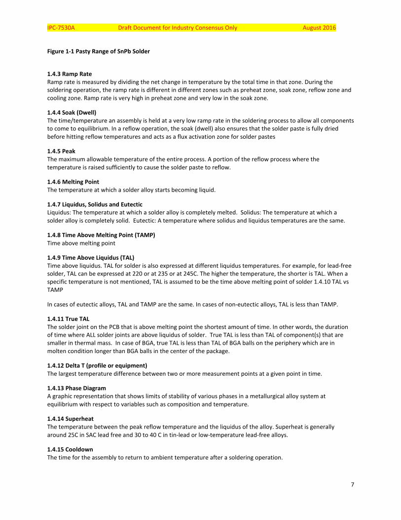
1.4.3 Pasty Range The semiliquid state between liquidus and solidus as the solder begins to solidify but is not yet completely solid and also when solder begins to melt but is not yet completely molten.
Figure 3.4 shows Eutectic temperature, super heat and pasty range. Eutectic temperature the lowest melting point possible for the alloy. It is lower than the melting point of any of the metals in the alloy. Even though eutectic is an alloy, it behaves like a metal in the sense that it has only one melting point just like a metal.
Pasty range is the temperature between the liquidus and solidus temperatures of an alloy. The range can be very small or very large depending on the composition of the alloy. As seen in Figure 1-1, either to the left or right of eutectic temperature, the pasty range is very small but it grows as the composition changes in either direction with changes in tin or lead content.
IPC-7530A Draft Document for Industry Consensus Only August 2016
7
Figure 1-1 Pasty Range of SnPb Solder
1.4.3 Ramp Rate Ramp rate is measured by dividing the net change in temperature by the total time in that zone. During the soldering operation, the ramp rate is different in different zones such as preheat zone, soak zone, reflow zone and cooling zone. Ramp rate is very high in preheat zone and very low in the soak zone.
1.4.4 Soak (Dwell) The time/temperature an assembly is held at a very low ramp rate in the soldering process to allow all components to come to equilibrium. In a reflow operation, the soak (dwell) also ensures that the solder paste is fully dried before hitting reflow temperatures and acts as a flux activation zone for solder pastes
1.4.5 Peak The maximum allowable temperature of the entire process. A portion of the reflow process where the temperature is raised sufficiently to cause the solder paste to reflow.
1.4.6 Melting Point The temperature at which a solder alloy starts becoming liquid.
1.4.7 Liquidus, Solidus and Eutectic Liquidus: The temperature at which a solder alloy is completely melted. Solidus: The temperature at which a solder alloy is completely solid. Eutectic: A temperature where solidus and liquidus temperatures are the same.
1.4.8 Time Above Melting Point (TAMP) Time above melting point
1.4.9 Time Above Liquidus (TAL) Time above liquidus. TAL for solder is also expressed at different liquidus temperatures. For example, for lead-free solder, TAL can be expressed at 220 or at 235 or at 245C. The higher the temperature, the shorter is TAL. When a specific temperature is not mentioned, TAL is assumed to be the time above melting point of solder 1.4.10 TAL vs TAMP
In cases of eutectic alloys, TAL and TAMP are the same. In cases of non-eutectic alloys, TAL is less than TAMP.
1.4.11 True TAL The solder joint on the PCB that is above melting point the shortest amount of time. In other words, the duration of time where ALL solder joints are above liquidus of solder. True TAL is less than TAL of component(s) that are smaller in thermal mass. In case of BGA, true TAL is less than TAL of BGA balls on the periphery which are in molten condition longer than BGA balls in the center of the package.
1.4.12 Delta T (profile or equipment) The largest temperature difference between two or more measurement points at a given point in time.
1.4.13 Phase Diagram A graphic representation that shows limits of stability of various phases in a metallurgical alloy system at equilibrium with respect to variables such as composition and temperature.
1.4.14 Superheat The temperature between the peak reflow temperature and the liquidus of the alloy. Superheat is generally around 25C in SAC lead free and 30 to 40 C in tin-lead or low-temperature lead-free alloys.
1.4.15 Cooldown The time for the assembly to return to ambient temperature after a soldering operation.
IPC-7530A Draft Document for Industry Consensus Only August 2016
8
1.4.16 Preheat The section of the soldering equipment which establishes the ramp rate for an assembly before the soak.
A profile zone where the assembly is heated from room temperature to the beginning of the soak zone temperature and is characterized by the ramp slope measurement.
1.4.17 Class 1 Radiant IR-Dominant Systems Heating of the assembly is accomplished predominantly by infrared (IR) radiation with little or no convection.
1.4.18 Class 2 Convection/IR Systems Heating of the assembly is accomplished by a combination of IR radiation and convection in varying ratios.
1.4.19 Class 3 Convection-Dominant Systems Heating of the assembly is accomplished predominantly by convection with little or no IR.
1.4.20 Profile Zones The profile is divided into distinct time periods which represent portions of the thermal process. Each zone is characterized by one or more measurements extracted from each zone (e.g., temperature, slope or time value).
2 APPLICABLE DOCUMENTS 2.1 IPC1 IPC-T-50 Terms and Definitions for Interconnecting and Packaging Electronic Circuits
IPC-CA-821 General Requirements for Thermally Conductive Adhesives
IPC-2222 Sectional Design Standard for Rigid Organic Printed Boards
IPC-9501 PWB Assembly Process Simulation for Evaluation of Electronic Components
IPC-9502 PWB Assembly Soldering Process Guideline for Electronic Components
IPC-9504 Assembly Process Simulation for Evaluation of Non-IC Components (Preconditioning Non-IC Components)
2.2 Joint Industry Standard2 J-STD-001 Requirements for Soldered Electrical and Electronic Assemblies
J-STD-002 Solderability Tests for Component Leads, Terminations, Lugs, Terminals and Wires
2.3 Other Industry Standard JEP 140 Beaded Thermocouple Temperature Measurement of Semiconductor Packages
3 CONVECTION REFLOW PROFILING
3.1 Time/Temperature Profiles The solder profile, also known as thermal profile, is one of the key variables in the manufacturing process that
IPC-7530A Draft Document for Industry Consensus Only August 2016
9
significantly impacts product yield, quality and reliability. Conveyor speed and panel temperatures are two variables in solder profile development. The solder profile is not only product specific; it is also flux and solder alloy dependent. Different pastes require different profiles for optimum performance, so it is important to consult the paste manufacturer before developing the solder profile.
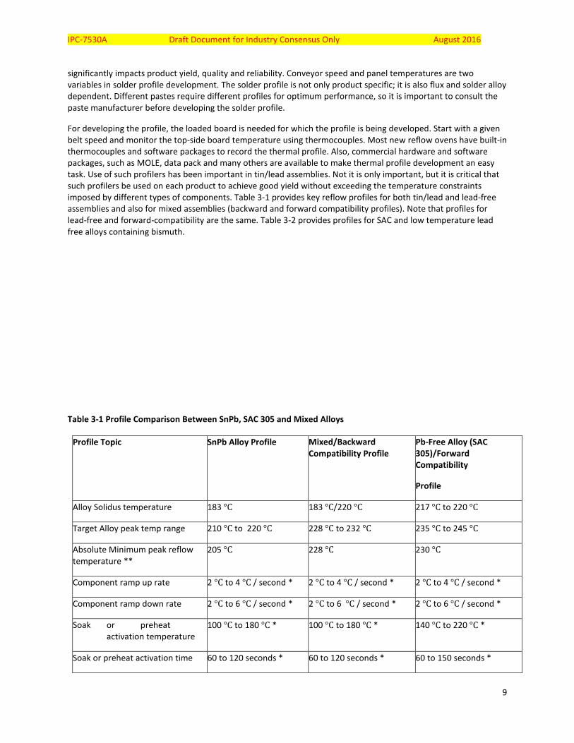
For developing the profile, the loaded board is needed for which the profile is being developed. Start with a given belt speed and monitor the top-side board temperature using thermocouples. Most new reflow ovens have built-in thermocouples and software packages to record the thermal profile. Also, commercial hardware and software packages, such as MOLE, data pack and many others are available to make thermal profile development an easy task. Use of such profilers has been important in tin/lead assemblies. Not it is only important, but it is critical that such profilers be used on each product to achieve good yield without exceeding the temperature constraints imposed by different types of components. Table 3-1 provides key reflow profiles for both tin/lead and lead-free assemblies and also for mixed assemblies (backward and forward compatibility profiles). Note that profiles for lead-free and forward-compatibility are the same. Table 3-2 provides profiles for SAC and low temperature lead free alloys containing bismuth.
Table 3-1 Profile Comparison Between SnPb, SAC 305 and Mixed Alloys
Profile Topic SnPb Alloy Profile Mixed/Backward Compatibility Profile
Pb-Free Alloy (SAC 305)/Forward Compatibility
Profile
Alloy Solidus temperature 183 °C 183 °C/220 °C 217 °C to 220 °C
Target Alloy peak temp range 210 °C to 220 °C 228 °C to 232 °C 235 °C to 245 °C
Absolute Minimum peak reflow temperature **
205 °C 228 °C 230 °C
Component ramp up rate 2 °C to 4 °C / second * 2 °C to 4 °C / second * 2 °C to 4 °C / second *
Component ramp down rate 2 °C to 6 °C / second * 2 °C to 6 °C / second * 2 °C to 6 °C / second *
Soak or preheat activation temperature
100 °C to 180 °C * 100 °C to 180 °C * 140 °C to 220 °C *
Soak or preheat activation time 60 to 120 seconds * 60 to 120 seconds * 60 to 150 seconds *
IPC-7530A Draft Document for Industry Consensus Only August 2016
10
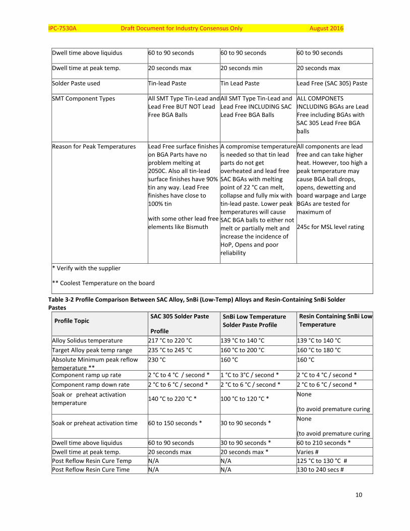
Dwell time above liquidus 60 to 90 seconds 60 to 90 seconds 60 to 90 seconds
Dwell time at peak temp. 20 seconds max 20 seconds min 20 seconds max
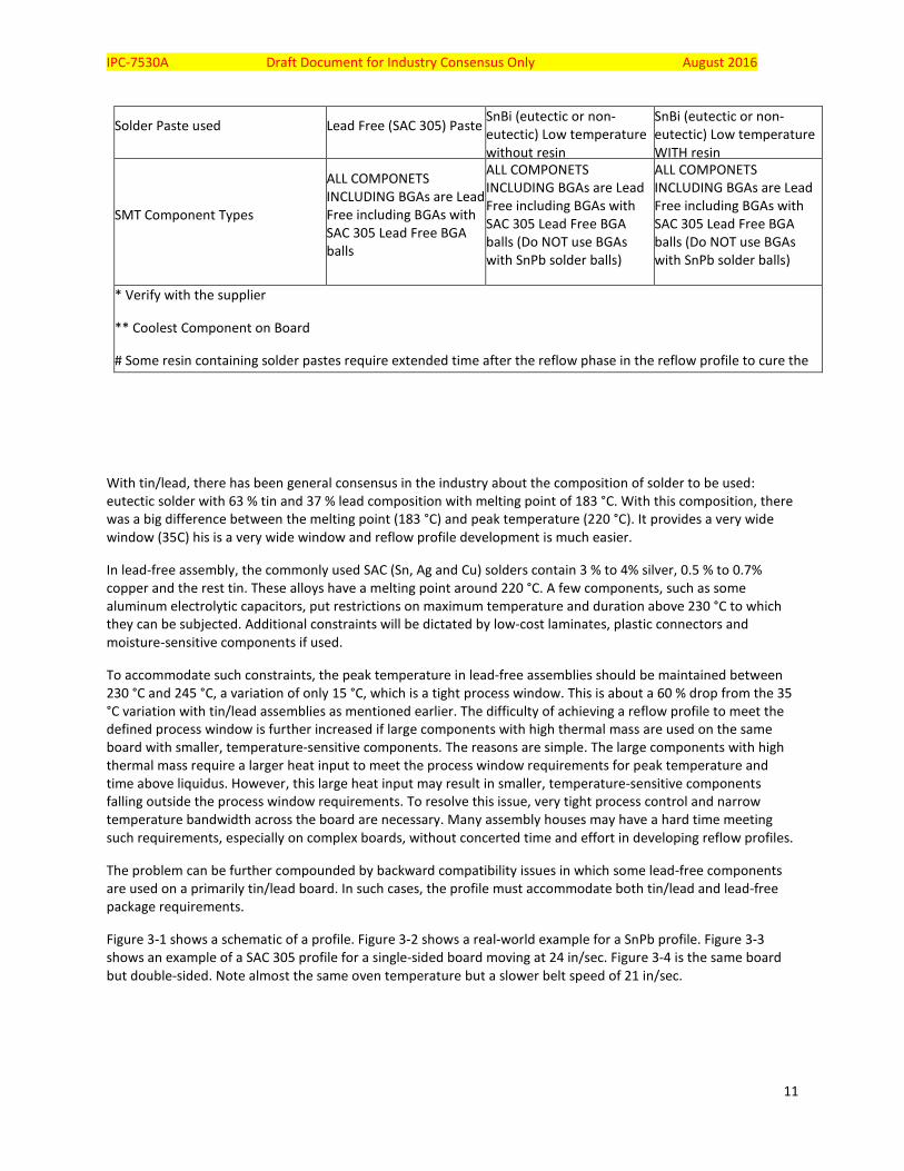
Solder Paste used Tin-lead Paste Tin Lead Paste Lead Free (SAC 305) Paste
SMT Component Types All SMT Type Tin-Lead and Lead Free BUT NOT Lead Free BGA Balls
All SMT Type Tin-Lead and Lead Free INCLUDING SAC Lead Free BGA Balls
ALL COMPONETS INCLUDING BGAs are Lead Free including BGAs with SAC 305 Lead Free BGA balls
Reason for Peak Temperatures Lead Free surface finishes on BGA Parts have no problem melting at 2050C. Also all tin-lead surface finishes have 90% tin any way. Lead Free finishes have close to 100% tin
with some other lead free elements like Bismuth
A compromise temperature is needed so that tin lead parts do not get overheated and lead free SAC BGAs with melting point of 22 °C can melt, collapse and fully mix with tin-lead paste. Lower peak temperatures will cause SAC BGA balls to either not melt or partially melt and increase the incidence of HoP, Opens and poor reliability
All components are lead free and can take higher heat. However, too high a peak temperature may cause BGA ball drops, opens, dewetting and board warpage and Large BGAs are tested for maximum of
245c for MSL level rating
* Verify with the supplier
** Coolest Temperature on the board
Table 3-2 Profile Comparison Between SAC Alloy, SnBi (Low-Temp) Alloys and Resin-Containing SnBi Solder Pastes
Profile Topic SAC 305 Solder Paste
Profile
SnBi Low Temperature Solder Paste Profile
Resin Containing SnBi Low Temperature
Alloy Solidus temperature 217 °C to 220 °C 139 °C to 140 °C 139 °C to 140 °C Target Alloy peak temp range 235 °C to 245 °C 160 °C to 200 °C 160 °C to 180 °C Absolute Minimum peak reflow temperature **
230 °C 160 °C 160 °C
Component ramp up rate 2 °C to 4 °C / second * 1 °C to 3°C / second * 2 °C to 4 °C / second * Component ramp down rate 2 °C to 6 °C / second * 2 °C to 6 °C / second * 2 °C to 6 °C / second * Soak or preheat activation temperature 140 °C to 220 °C * 100 °C to 120 °C *
None
(to avoid premature curing
Soak or preheat activation time 60 to 150 seconds * 30 to 90 seconds * None
(to avoid premature curing Dwell time above liquidus 60 to 90 seconds 30 to 90 seconds * 60 to 210 seconds *
Dwell time at peak temp. 20 seconds max 20 seconds max * Varies #
Post Reflow Resin Cure Temp N/A N/A 125 °C to 130 °C # Post Reflow Resin Cure Time N/A N/A 130 to 240 secs #
IPC-7530A Draft Document for Industry Consensus Only August 2016
11
Solder Paste used Lead Free (SAC 305) Paste SnBi (eutectic or non-eutectic) Low temperature without resin
SnBi (eutectic or non-eutectic) Low temperature WITH resin
SMT Component Types
ALL COMPONETS INCLUDING BGAs are Lead Free including BGAs with SAC 305 Lead Free BGA balls
ALL COMPONETS INCLUDING BGAs are Lead Free including BGAs with SAC 305 Lead Free BGA balls (Do NOT use BGAs with SnPb solder balls)
ALL COMPONETS INCLUDING BGAs are Lead Free including BGAs with SAC 305 Lead Free BGA balls (Do NOT use BGAs with SnPb solder balls)
* Verify with the supplier
** Coolest Component on Board
# Some resin containing solder pastes require extended time after the reflow phase in the reflow profile to cure the
With tin/lead, there has been general consensus in the industry about the composition of solder to be used: eutectic solder with 63 % tin and 37 % lead composition with melting point of 183 °C. With this composition, there was a big difference between the melting point (183 °C) and peak temperature (220 °C). It provides a very wide window (35C) his is a very wide window and reflow profile development is much easier.
In lead-free assembly, the commonly used SAC (Sn, Ag and Cu) solders contain 3 % to 4% silver, 0.5 % to 0.7% copper and the rest tin. These alloys have a melting point around 220 °C. A few components, such as some aluminum electrolytic capacitors, put restrictions on maximum temperature and duration above 230 °C to which they can be subjected. Additional constraints will be dictated by low-cost laminates, plastic connectors and moisture-sensitive components if used.
To accommodate such constraints, the peak temperature in lead-free assemblies should be maintained between 230 °C and 245 °C, a variation of only 15 °C, which is a tight process window. This is about a 60 % drop from the 35 °C variation with tin/lead assemblies as mentioned earlier. The difficulty of achieving a reflow profile to meet the defined process window is further increased if large components with high thermal mass are used on the same board with smaller, temperature-sensitive components. The reasons are simple. The large components with high thermal mass require a larger heat input to meet the process window requirements for peak temperature and time above liquidus. However, this large heat input may result in smaller, temperature-sensitive components falling outside the process window requirements. To resolve this issue, very tight process control and narrow temperature bandwidth across the board are necessary. Many assembly houses may have a hard time meeting such requirements, especially on complex boards, without concerted time and effort in developing reflow profiles.
The problem can be further compounded by backward compatibility issues in which some lead-free components are used on a primarily tin/lead board. In such cases, the profile must accommodate both tin/lead and lead-free package requirements.
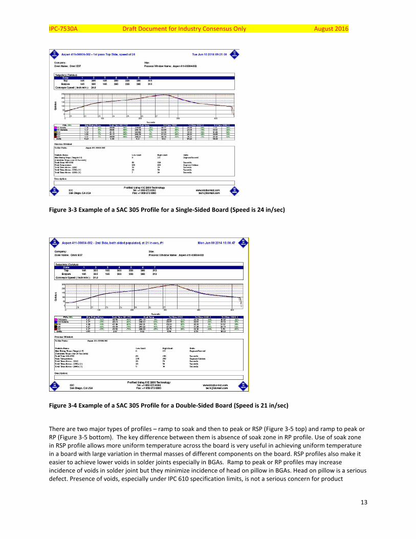
Figure 3-1 shows a schematic of a profile. Figure 3-2 shows a real-world example for a SnPb profile. Figure 3-3 shows an example of a SAC 305 profile for a single-sided board moving at 24 in/sec. Figure 3-4 is the same board but double-sided. Note almost the same oven temperature but a slower belt speed of 21 in/sec.

IPC-7530A Draft Document for Industry Consensus Only August 2016
12
Figure 3-1 Schematic of Reflow Profile
Figure 3-2 SnPb Profile With Multiple Thermocouples
IPC-7530A Draft Document for Industry Consensus Only August 2016
13
Figure 3-3 Example of a SAC 305 Profile for a Single-Sided Board (Speed is 24 in/sec)
Figure 3-4 Example of a SAC 305 Profile for a Double-Sided Board (Speed is 21 in/sec)
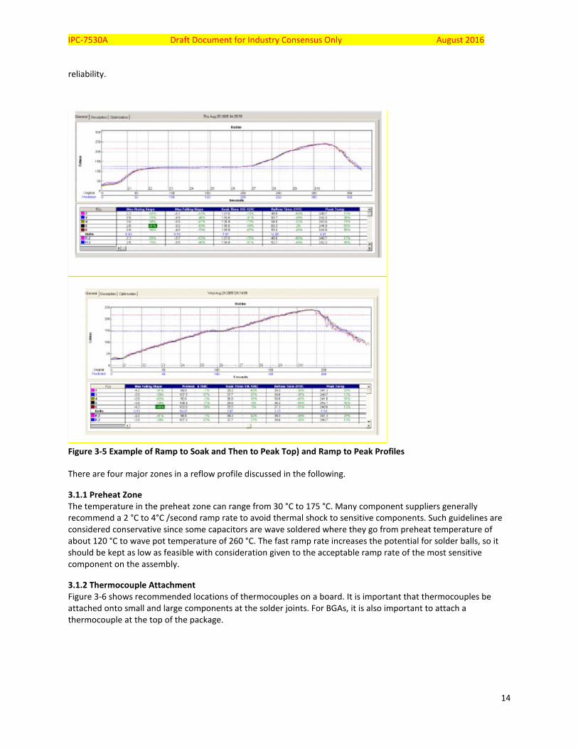
There are two major types of profiles – ramp to soak and then to peak or RSP (Figure 3-5 top) and ramp to peak or RP (Figure 3-5 bottom). The key difference between them is absence of soak zone in RP profile. Use of soak zone in RSP profile allows more uniform temperature across the board is very useful in achieving uniform temperature in a board with large variation in thermal masses of different components on the board. RSP profiles also make it easier to achieve lower voids in solder joints especially in BGAs. Ramp to peak or RP profiles may increase incidence of voids in solder joint but they minimize incidence of head on pillow in BGAs. Head on pillow is a serious defect. Presence of voids, especially under IPC 610 specification limits, is not a serious concern for product
IPC-7530A Draft Document for Industry Consensus Only August 2016
14
reliability.
Figure 3-5 Example of Ramp to Soak and Then to Peak Top) and Ramp to Peak Profiles There are four major zones in a reflow profile discussed in the following.
3.1.1 Preheat Zone The temperature in the preheat zone can range from 30 °C to 175 °C. Many component suppliers generally recommend a 2 °C to 4°C /second ramp rate to avoid thermal shock to sensitive components. Such guidelines are considered conservative since some capacitors are wave soldered where they go from preheat temperature of about 120 °C to wave pot temperature of 260 °C. The fast ramp rate increases the potential for solder balls, so it should be kept as low as feasible with consideration given to the acceptable ramp rate of the most sensitive component on the assembly.
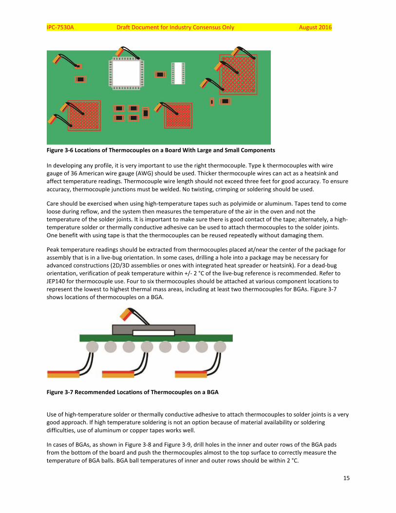
3.1.2 Thermocouple Attachment Figure 3-6 shows recommended locations of thermocouples on a board. It is important that thermocouples be attached onto small and large components at the solder joints. For BGAs, it is also important to attach a thermocouple at the top of the package.
IPC-7530A Draft Document for Industry Consensus Only August 2016
15
Figure 3-6 Locations of Thermocouples on a Board With Large and Small Components In developing any profile, it is very important to use the right thermocouple. Type k thermocouples with wire gauge of 36 American wire gauge (AWG) should be used. Thicker thermocouple wires can act as a heatsink and affect temperature readings. Thermocouple wire length should not exceed three feet for good accuracy. To ensure accuracy, thermocouple junctions must be welded. No twisting, crimping or soldering should be used.
Care should be exercised when using high-temperature tapes such as polyimide or aluminum. Tapes tend to come loose during reflow, and the system then measures the temperature of the air in the oven and not the temperature of the solder joints. It is important to make sure there is good contact of the tape; alternately, a high-temperature solder or thermally conductive adhesive can be used to attach thermocouples to the solder joints. One benefit with using tape is that the thermocouples can be reused repeatedly without damaging them.
Peak temperature readings should be extracted from thermocouples placed at/near the center of the package for assembly that is in a live-bug orientation. In some cases, drilling a hole into a package may be necessary for advanced constructions (2D/3D assemblies or ones with integrated heat spreader or heatsink). For a dead-bug orientation, verification of peak temperature within +/- 2 °C of the live-bug reference is recommended. Refer to JEP140 for thermocouple use. Four to six thermocouples should be attached at various component locations to represent the lowest to highest thermal mass areas, including at least two thermocouples for BGAs. Figure 3-7 shows locations of thermocouples on a BGA.
Figure 3-7 Recommended Locations of Thermocouples on a BGA
Use of high-temperature solder or thermally conductive adhesive to attach thermocouples to solder joints is a very good approach. If high temperature soldering is not an option because of material availability or soldering difficulties, use of aluminum or copper tapes works well.
In cases of BGAs, as shown in Figure 3-8 and Figure 3-9, drill holes in the inner and outer rows of the BGA pads from the bottom of the board and push the thermocouples almost to the top surface to correctly measure the temperature of BGA balls. BGA ball temperatures of inner and outer rows should be within 2 °C.
IPC-7530A Draft Document for Industry Consensus Only August 2016
16
Proper attachment is critical to ensure an accurate temperature measurement is achieved. There are various methods for attaching thermocouples to assemblies for profiling.
Figure 3-8 Example of TC on Inner and Outer Rows – Drilling From Bottom of BGA and Other Components

IPC-7530A Draft Document for Industry Consensus Only August 2016
17
Figure 3-9 Example of TC on Inner and Outer Rows – Drilling From Bottom of BGA and Other Components
3.1.3 Soak Zone The soak zone is intended to bring the temperature of the entire board up to a uniform temperature. The ramp rate in this zone (100 to 180 C for tin lead and 140 to 220 C for SAC lead free) is much slower. The soak zone also acts as the flux activation zone for solder paste. The consequences of having too high a temperature in the soak zone can include: solder balls, solder splatter due to excessive oxidation of paste and spent flux activation capability. The purpose of long soak zone is to minimize voids, especially in BGAs. It is also common practice not to use soak zone but to steadily ramp the temperature from preheat zone to peak reflow. However, the likelihood of voids may be increased when ramping steadily to peak reflow temperature.
3.1.4 Reflow Zone The peak temperature in the reflow zone should be high enough to obtain good wetting, and create a strong metallurgical bond. It should not be so high as to cause component or board damage or discoloration or, in worst case, delamination or charring of the board. Too low temperature may result in cold and grainy solder joints, nonmelted solder or poor intermetallic bonding. As shown in Table 7-3, the peak temperature in this zone should be maintained between 210 °C to 220 °C for tin lead and 230 °C to 245 °C for lead-free solder alloy. TAL should be
IPC-7530A Draft Document for Industry Consensus Only August 2016
18
60 to 90 seconds but closer to 60 seconds. Extended duration above the solder melting point or TAL will damage temperature-sensitive components. It also results in excessive intermetallic growth, which makes the solder joint brittle and reduces solder joint fatigue resistance.
3.1.5 Cooling Zone The typical cooling rate for most assemblies has been 4 °C to 6 °C per second, driven primarily by throughput and SnPb intermetallic thickness concerns. With the transition to Pb-free solders the pad cratering defect has become more common due to the increased stiffness of SAC solders and the reduction in the flexure resistance and fracture toughness of laminates. Pad cratering has been identified directly after the reflow process, leading to several experiments designed to understand the impact of cooling rate. Among others such as package warpage, pad cratering is one of the reasons for many companies using lower temperature lead free solders containing bismuth (Table 3-1)
During the cooling phase, the various materials will cool at different rates. The BGA package typically will cool faster than the solder joint and much faster than the PCB. This differential cooling can create mechanical strain on the weakest spot in the interconnect, the laminate below the BGA pad. By slowing the cooling rate significantly, to as low as 1.5 °C per second, all of the materials will cool more slowly and will reduce the strain placed on the laminate. Experimental work performed by consortia has shown that this slowed cooling does not appear to negatively impact solder joint intermetallics nor the grain structure of the joint. If pad cratering is found immediately after reflow or if the assembly is determined to be at risk for cratering, then the cooling rate of the PCBA should be slowed to reduce strain.
3.1.6 Thermal Profile for Backward Compatibility Developing a reflow profile is made difficult when dealing with backward compatibility issues in which some lead-free components are used on a primarily tin/lead board. Backward compatibility is a scenario in which some components are available only with lead-free surface finishes. Such a scenario arises since it may not be economical for many component suppliers to supply both tin/lead and lead-free versions of the same component. It is not an issue when using leaded components such as small outline integrated circuit (SOIC), plastic leaded chip carrier (PLCC) or fine pitch with lead-free surface finishes. Most tin/lead components primarily have 85 % tin surface finish with about 15 % lead.
The real problem arises when using lead-free BGAs on a primarily tin/lead board. If the tin/lead profile with maximum peak temperature of 220 °C is used, the lead-free BGA balls will not reflow at all or will partially reflow, creating a serious solder joint reliability problem.
If tin/lead components are soldered along with some lead-free BGAs in the same oven (since tin/lead versions are not available), a peak temperature must be used that is not damaging to all the tin/lead components, but is also sufficient to reflow the lead-free BGAs. Using tin/lead solder paste is appropriate, since most of the components on the board are tin/lead. As shown in Table 3-1, peak temperature of 210 °C to 220 °C will be fine for tin/lead but inadequate for lead-free BGA balls with a melting point of 217 °C to 221 °C. But a peak temperature of 228 °C to 232 °C with 60 to 90 seconds TAL will be sufficient to reflow lead-free BGAs without seriously damaging all the tin/lead components on the same board.
If the tight reflow temperature band of 228 °C to 232 °C is difficult to achieve to solder both tin/lead and lead-free BGAs in backward compatibility scenarios, then consider selective laser soldering to solder lead-free BGAs after other tin lead components have been soldered in a convection reflow oven or find an alternative source for BGAs with tin/lead balls.
3.1.7 Unique Profile for Each PWBA A reflow program is not the same as a reflow profile. A reflow program is the combination of machine settings and conveyor speed, while a reflow profile is the visual representation of the time and temperature that a thermocouple sees during a PWBA’s travel through the reflow oven. Every unique PWBA needs to be profiled to show that all locations on the board meet the various requirements for creating acceptable solder joints. A single program will produce very different profiles for different, unique PWBAs. There is some misunderstanding that one
IPC-7530A Draft Document for Industry Consensus Only August 2016
19
oven profile will work for all boards, so there is no need to develop unique profiles for each board. This is not true, because each board has a unique thermal mass or different loading patterns (distance between boards as they are loaded in the oven). A double-sided board, depending on component placement and distribution of copper planes, will require a different profile for each side. Profiles may look the same for many PWBAs but will generally require different machine programs to create these similar profiles. It is common to have a small number of standard machine programs, but it must be shown that a specific program produces an acceptable profile.
Once the program has been optimized to create the desired profile, it is recommended that an actual production board with solder paste and components for reflow be created. After reflow, inspect the quality of the solder joints to verify that the solder joints across all of the various components meet the requirements of the IPC-A-610 and any customer specific requirements. A random problem only in a specific section of the board may be related to solderability; a consistent problem in a given section may be related to the solder profile due to nonuniform heating (wide bandwidth). Consistent problems may also be related to paste quality and land pattern design.
Once the program is found to give the desired results (assuming design and other material variables have been optimized), document the program. After this point, no changes should be allowed in the program and the resulting profile.
3.1.8 Flux Flux has two key functions. First it must remove contamination and oxides from the PCB and component surfaces and create a suitable nonoxidized metal surface. Second it must protect that metal surface from reoxidation during heating. A common mistake is to use a time/temperature profile that consumes the flux before the solder melts. Ideally, the flux would be activated just as the solder begins to melt. Activation time should range from 90 to 120 seconds. Flux usually becomes active at around 130 °C for tin/lead solder pastes. Typically, solder paste activation for lead-free solder will be higher (in the 150 °C range); however, it is recommended to review the data sheet from solder paste supplier. It is important to select a flux and solder alloy that works well with the lead finish being used.
3.2 Material Issues Components can be damaged by the incorrect application of heat. All components have a heat exposure limit. Most tin/lead surface mount components should tolerate a peak temperature of 220 °C for up to 60 seconds. Lead-free BGAs will be rated to a higher temperature, which is approximately 240 °C to 260 °C. Thermal shock, caused by the rapid application of heat, can crack certain components. However, since the peak temperature of reflow ovens varies, the intent is to heat the solder in a controlled established profile to a solder joint temperature of 210 °C to 220 °C for tin/lead products and for 235 °C to 245 °C for lead-free products.
Refer to J-STD-020 for further information on reflow sensitivity of nonhermetic solid state surface mount devices.
Component lead finish will affect solderability. There are a number of lead finishes being used today, including tin/lead, gold, tin and palladium. It is important to select a flux and solder alloy that works well with the lead finish being used.
3.3 Reflow Soldering When profiling assemblies for solder reflow and adhesive cure, the following areas shall be monitored as seen earlier in Figure 3-1 for solder paste.
Note: An example of adhesive, underfill or other material curing profile is shown in Figure 3-10.
Ramp: This is the portion of the profile where the assembly is heated from ambient temperature at a predetermined rate. Controlling the ramp is necessary to prevent component damage. It also allows the flux solvents to evaporate prior to the flux being fully active.
IPC-7530A Draft Document for Industry Consensus Only August 2016
20
Figure 3-10 Curing Profile Soak Time: The time is monitored to ensure temperature equilibrium across the assembly. This portion of the profile also allows time to drive off volatile ingredients within the solder paste and activate the paste’s flux to remove oxides. CAUTION: Use of a soak zone in a reflow profile is helpful for reducing voids in BGA solder joints but may increase the incidence of HoP in BGAs. Ramp to peak profile should be considered to minimize HoP.
which the solder alloy is liquidus. The assembly must spend enough time in this state to ensure all areas of the assembly reach soldering temperature. TAL for eutectic solder may be shorter than TAL for noneutectic solder since noneutectic alloys have both solidus and liquidus temperatures but eutectic solders have the same solidus and liquidus temperatures.
Peak/Spike Temperature: Peak temperature is the maximum temperature recorded by the thermocouple for the monitored location. Excessive temperatures could result in component and PWB damage.
Cure Period: Cure period is monitored to ensure proper curing of the adhesive.
3.3.1 True Time Above Liquidus (TAL) It is important to understand the difference between TAL and true TAL to minimize incidence of Head on Pillow in BGAs. See Figure 3-11 and Figure 3-12. When we attach thermocouples to the inner and out balls of BGA, it is common to find that the temperature of the outer row of BGA balls are higher than the temperature of inner row balls, resulting in time delay (LTD, Figure 3-11) between outer and inner row balls melting.

IPC-7530A Draft Document for Industry Consensus Only August 2016
21
Figure 3-11 Role of Liquidus Time Delay in Head on Pillow Note: True TAL (in green) is less than total TAL. Liquidus time delay is the time that some balls were not above liquidus temperature.
Figure 3-12 Standard TAL vs True TAL Note: True TAL is less than TAL.
Another way to describe true TAL is the time at which every component, no matter how large, is above the melting point of solder. True TAL is also the time when all the points of measure are above liquidus at the same time, or the smaller number. This is critical, especially with large BGAs, in which outer balls have longer TAL and inner balls may have lower TAL.
It is only during this time that the component is free to self-align. Any one location's TAL does not measure the actual time the entire component is free to self-align, hence the need for true TAL measurement.
IPC-7530A Draft Document for Industry Consensus Only August 2016
22
The time difference between inner and outer balls becoming liquidus is called Liquidus Time Delay (LTD), and plays a critical role in HoP. Hence True TAL must be sufficient for ALL balls (60 seconds). Also to minimize HoP, avoid too long soak and ensure min 235oC Peak for all balls. When dealing with backward compatibility situations, (lead free BGAs being soldered with predominantly tin lead components and solder paste because tin lead BGAs may not be available) strive for 232oC minimum peak. To minimize HoP, use ramp to peak profile instead of ramp to soak profile but do understand that ramp to peak profile may result in more voids in BGAs. It is a balancing act but voids are not serious defects, but HoPs are. Here are some specific Reflow Guidelines for Lead Free, Peak and TAL
1. Peak Target 235 to 245 C but aim for 240+/- 2C 2. TAL Target above 220C: 60 to 90 Seconds. Shoot for 70 Seconds 3. True TAL Target: 60 Seconds for All BGA Balls 4. TAL Target above 235: 20-30 Seconds. Shoot for 20 Seconds 5. TAL Target above 240 C: 5 to 15 Seconds. Shoot for 10 Seconds
Fine point note: It is understood that over the area of large components not all locations of that component will reach liquidus at the same time; some later than others.
3.4 Equipment Settings
3.4.1 Reflow Oven Selection Reflow ovens are available in various sizes and configurations. When selecting the most appropriate reflow oven for a particular purpose, many variables should be taken into account in terms of types of devices being assembled and types of configurations/options. Such options that should be reviewed in terms of a product application include:
• Size of product
• Desired throughput
• Types of solders
• Types of fluxes
• Cost of assembly
Such options to be considered regarding ovens include:
• IR or convection number of heating zones
• Clearance height
• Cover gas
• Conveyor belt type
• Belt width
• On-board profiling ability
• Product tracking

IPC-7530A Draft Document for Industry Consensus Only August 2016
23
• Edge-rail or center-support capability
Some of these options will be discussed in 3.4.2 through 3.4.7.
3.4.2 IR vs Convection Reflow ovens are typically either IR or convection reflow. In an IR oven, ceramic heaters are used to transfer heat to the assembly using radiation. In a convection reflow process, fans are used to force heated air to the assembly. Recent advances in reflow processes and oven configurations have evolved the use of vacuum reflow. Vacuum reflow helps in applications which require very low levels of solder voiding in the attachment of a device.
3.4.3 Heating Zone Selection The number of heating zones in standard reflow ovens range anywhere from seven to 12 and possibly more. There are usually top and bottom heaters that can be set independently when setting up a reflow profile. For lead-free applications, a minimum of seven heating zones should be selected. For reflow ovens that are being put in line with other pieces of equipment, throughput may be another consideration in terms of length of the oven and number of heating zones needed to balance throughput with an optimal reflow profile.
3.4.4 Clearance Height/Conveyor Belt Type/Conveyor Belt Width/Edge-Rail Support In terms of a clearance height selection, normally the oven clearance height is kept to a minimum to maintain consistent heating within and between zones. The height of the product needs to be taken into account when defining the clearance height required for a particular oven. The type of product being assembled also impacts whether the conveyor belt is fine-mesh or not. If a device is fairly small, a fine-mesh belt may be needed to eliminate the use of added fixturing to transfer the part through the oven. The necessary belt width also is determined by the size of the assembly passing through the oven. If an assembly is double-sided, edge rails can be added to the oven so additional fixturing may not be required to support the assembly above the conveyor belt and to allow for better airflow around the assembly.
3.4.5 Cover Gas Standard reflow ovens can be configured in such a way that either the oven is run in an open-atmosphere environment or with a cover gas such as nitrogen being used during reflow. Determining the need for using nitrogen gas is related to the type of flux in the solder paste for the particular application. It also depends on the plating on the PWB and the terminals of the ICs being assembled.
Nitrogen helps to slow oxidation or prevent reoxidation on metal surfaces. It also promotes better wetting during the reflow process, especially when soldering to NiAu and bare-copper lands. With advances in solder paste, the need for nitrogen has reduced, especially if an aggressive flux is used in the solder paste selected. This, however, can be a trade-off on whether a cleaning process is needed to remove flux residues. The major drawback of adding a nitrogen package to an oven is not only the initial cost of adding the feature but also the long-term cost of ownership of having house gas plumbed to the oven.
3.4.6 Profiling In most cases, reflow ovens are configured such that on-board reflow profiling can be accomplished. In this, one end of a thermal couple is attached to the oven, and the other end of the thermal couple is attached to the product traveling through the oven. This option eliminates the need for the purchase of an added data recorder for profiling capability.
3.4.7 Product Trackers Ovens can also be configured with product trackers to allow for traceability of parts through a reflow oven. These trackers have sensors mounted at the entrance and exit of an oven to sense when a product enters and exits the oven.
IPC-7530A Draft Document for Industry Consensus Only August 2016
24
4 VAPOR PHASE REFLOW PROFILING There are many driving forces for the use of vapor-phase soldering (VPS), also known as condensation soldering:
• Fixed peak temperature (215 °C or 230 °C) o Includes very large and small components with wide variances in thermal mass o Large and small components both achieve almost the same peak temperature
• Temperature-sensitive components • Pb-free alloys with higher melting points • Excellent heat-transfer capability • Inert environment • Vacuum capability (in some machines) • Preheat as an integral part of the machine • Possibility for lower intermetallic (IMC) thickness due to lower peak temperature • Potential for lower voids if vacuum capability is used • Better PWBA cleanliness • Higher surface insulation values • VPS liquids can access tighter spaces to remove flux residues
Even with these driving forces, VPS has gone through changes in popularity. It was the process of choice in the early 1980s, but its use declined considerably for several reasons, including problems with the VPS process itself and improvements in IR processes. Convection-dominant IR system have been known to provide efficient heating without the inherent problems of VPS.
By the late 1980s, VPS almost disappeared entirely due to excessive incidences of wicking on leads of J- and gull-wing devices, which led to solder opens. This wicking was caused by the lead and the land heating at different rates during VPS; it was exacerbated by noncoplanarity (the failure of the lead to touch the land). The surface of the lead reached the solder melting point a few seconds before the surface of the land, which caused the solder paste to melt, wet and wick up the lead before the land became hot enough for the molten solder to wet it. By the time the land reached the melting point of the solder paste, there was not enough solder left on the land to form a good solder joint. In addition to wicking in leaded parts, especially J-lead devices, VPS has also been known to cause tombstoning in chip components.
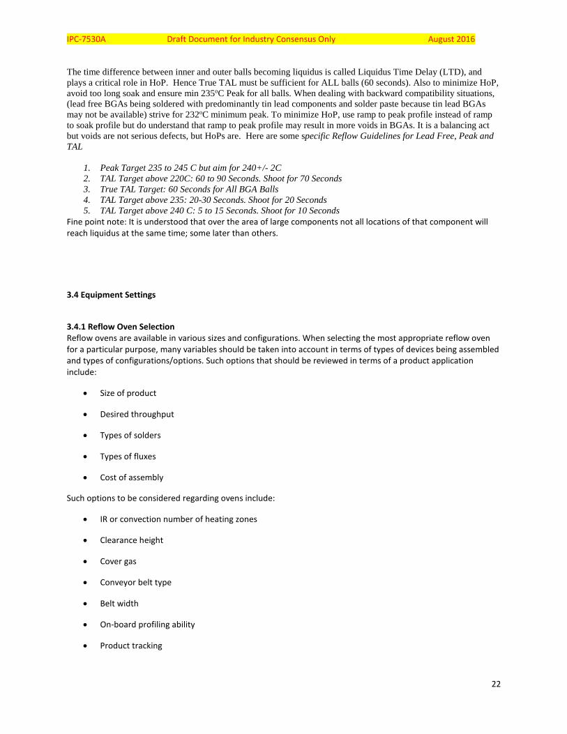
Figure 4-1 shows a VPS profile showing the leads reaching melting point temperature sooner than the pad. This time delay in reaching melting point for J-leaded components caused wicking and opens in solder joints. Newer VPS systems with built-in preheat have made this wicking less of a concern (see Figure 4-2). Additionally, the superheat (temperature between melting point and Peak Reflow) is significantly reduced in Pb-free processes to around 40 °C in SnPb alloys and around 20 °C in SAC Pb-free alloys.
VPS uses the latent heat of liquid vaporization to provide heat for soldering. This latent heat is released as the vapor of the inert liquid condenses on component leads and PCB lands. This liquid produces a dense, saturated vapor that displaces air and moisture. The temperature of the saturated vapor zone is the same as the boiling point of the vapor phase liquid. This fluid does not have any environmental concerns.
IPC-7530A Draft Document for Industry Consensus Only August 2016
25
Figure 4-1 VPS Profile Showing Wicking and Opens
IPC-7530A Draft Document for Industry Consensus Only August 2016
26
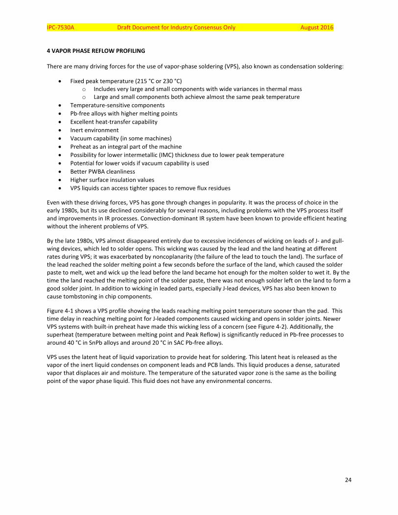
Figure 4-2 Profile for VPS With Preheat Resembles Convection Profile
Vapor-phase reflow can be operated as a single- or two-fluid system, utilizing a primary and a secondary fluid. The process was developed using the two-fluid approach in batch equipment, but modern in-line systems are normally operated with only one fluid. Whichever system is used, the maximum temperature reached by assemblies in VPS reflow depends on the choice of the primary fluid. Primary fluids are available in a number of temperature ranges, with 218 °C to 222 °C being common with SnPb solder and 235 °C to 245 ºC being common with lead-free solder. While all the primary fluids can be classified as perfluorocarbons, the basic structure (amine, cyclic or ether) will determine the key properties of in-use stability, solder paste chemical solubility and overall process economics. The choice of a fluid is normally based on the melting point of the solder alloy to be reflowed.
For the range cited, lower temperatures are suitable for the typical SnPb or SnPbAg alloys used for standard attachment processes. The upper end of the range will permit reflow of high-Pb alloys, which are used to attach pins to PGA packages. Users faced with specialty alloy reflows have been successful in mixing two primary fluids to tailor a VPS for a specific stable boiling point. They have found that higher temperatures will permit shorter times, which may be advantageous with some solder pastes.
VPS heats uniformly, so no part on the board (irrespective of its geometry) exceeds the fluid-boiling temperature. This is suitable for soldering odd-shaped parts, flexible circuits, pins and connectors, as well as for reflowing SnPb and Pb-free surface-mount package leads.
It is important to note that the soak zone for convection is almost impossible to duplicate in VPS, and convection pastes with soak zone for activation may not work in VPS. Users typically address this issues by adding secondary cooling coils to VPS. This controls the rise in temperature by increasing the water circulation when the PCB enters the VPS chamber. Pastes for ramp-to-peak are also common for both of these systems.
The use of nitrogen in convection systems for soldering in an inert environment has increased due to the widespread use of low-solids and no-clean fluxes and solder pastes.
It is difficult to provide uniform heating in larger ceramic and plastic BGAs–even with convection-dominant systems–VPS is being considered because of its efficient and uniform heating characteristics. In the case of backward compatibility, you cannot go to a higher reflow temperature for just a few Pb-free components, as the majority of SnPb components are likely to be adversely affected. VPS is being considered as a solution to provide a middle-of-the-road compromise reflow profile to produce acceptable solder joints in both SnPb and Pb-free components.
Because VPS provides an inert soldering environment without the use of nitrogen, users are giving it another look. They have found VPS to be a suitable option for Pb-free soldering, low-volume niche applications or for boards with numerous large ceramic BGAs with practically no leaded or chip components. Although VPS has very efficient and uniform heating characteristics, it is unlikely it will reclaim its status from years ago.
4.1 Vapor-Phase Reflow Vapor-phase reflow can be operated as a single- or two-fluid system, utilizing a primary and a secondary fluid. The process was developed using the two-fluid approach in batch equipment; but modern in-line systems normally operate with only one fluid. Whichever system is used, the maximum temperature reached by assemblies in vapor-phase reflow depends on the choice of the primary fluid. Primary fluids are available in a number of temperature ranges, with 218 °C to 222 °C being common with tin-lead products and 235 °C to 245 °C for lead-free products.

IPC-7530A Draft Document for Industry Consensus Only August 2016
27
While all the primary fluids can be classed as perfluorocarbons, the basic structure (amine, cyclic or ether) will determine the key properties of in-use stability, solder paste chemicals solubility and overall process economics. The choice of a fluid is normally based on the melting point of the solder alloy to be reflowed.
For the range cited, the lower temperatures are suitable for the typical tin-lead or tin-lead-silver alloys used for standard attachment processes. The upper end of the range will permit reflow of high-lead alloys, which are used to attach pins to pin grid array (PGA) packages. Users faced with reflow of a specialty alloy have been successful in mixing two primary fluids to tailor a vapor-phase system for a specific stable boiling point. Higher temperatures will permit shorter times, which may be advantageous with some solder pastes.
The primary vapor phase should be inert and not introduce contaminants that must be removed later. Solder paste chemicals that dissolve in the fluid are carried in the high-boiling vapor then deposited onto the surface of the boards. Such residues tend to be difficult to remove. Minimizing solder paste residue in the primary fluid will maximize the lifetime of the fluid, prevent boiling point elevation due to dissolved paste ingredients and simplify cleaning.
The secondary vapor blanket was originally CFC-113, a lower-boiling fluorinated material, which formed a low-cost sacrificial “lid” over the costlier primary fluid. The constant exposure to the high-boiling primary fluid at the interface of the two fluids would cause the secondary fluid to undergo thermal decomposition at the interface, generating HCl (hydrochloric) and HF (hydrofluoric) acid vapors. These corrosive vapors often attacked the soldering equipment over time. While in theory the vapors could be absorbed in flux residues and cause problems for high-reliability products, this was rare in comparison to the attack on the equipment. With the phase-out of CFC-113, a low-boiling perfluorocarbon was introduced to replace it. This second-generation secondary blanket fluid was more stable than CFC-113 for prolonged exposure to the high-boiling vapor-phase fluids.
As surface mount technology grew, most users converted to the higher throughput in-line machines, which used the single-fluid approach. Defluxing after vapor-phase reflow should be done with either a polar solvent formulation or include an aqueous cleaning formulation that can ensure removal of all solder paste residues, with the choice of cleaning process based on the composition of the solder paste. Secondary factors influencing the decision would be compatibility and the component-to-PWB surface spacing. In addition, most companies gave serious thought to considering the potential chemical loss from using this type of equipment since many perfluorinated compounds are very long-lived global warming compounds.
5 WAVE SOLDERING PROFILING By definition, mass wave soldering implies creating many solder connections simultaneously in a semiautomated or automated process. Equipment designed for this task generally has four basic characteristics:
• Product conveyance
• Fluxing capability
• Preheating capability
• Molten pot of solder with a nozzle
The key feature of the wave soldering machine is the type of wave nozzle that is used, this will determine the quality of solder for both through-hole and surface-mount components. Solder waves commonly used are single-wave, or dual-wave where the first wave is turbulent either rough and also or oscillating-wave. The other key feature of a solder wave is whether the solder falls in one direction or in both directions back into the solder pot. In general, the number of defects (e.g., icicles or bridging) are much lower in waves where the solder falls only in one direction – backward.
IPC-7530A Draft Document for Industry Consensus Only August 2016
28
The differences between manufacturers are in the application of these basic concepts and the equipment controls. Each machine has unique characteristics that need to be taken into account when developing a thermal profile. Traditional wave soldering machines are used for mass soldering of through-hole and some surface-mount components (typically chip resistors and capacitors). When bottom-side surface-mount components are soldered, they are secured in place with a cured adhesive prior to soldering.
The wave soldering system automatically performs the soldering process, which is flux application, heating of the area to be soldered, application of molten solder and solidification, as all of these characteristics act together to ensure proper soldering. A solder recipe is developed by recording the optimum process parameters selected for conveyor speed, flux application, preheaters and solder temperature.
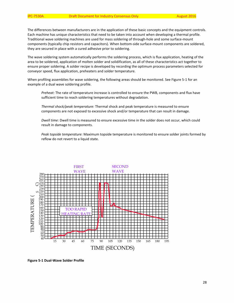
When profiling assemblies for wave soldering, the following areas should be monitored. See Figure 5-1 for an example of a dual wave soldering profile.
Preheat: The rate of temperature increase is controlled to ensure the PWB, components and flux have sufficient time to reach soldering temperatures without degradation. Thermal shock/peak temperature: Thermal shock and peak temperature is measured to ensure components are not exposed to excessive shock and/or temperature that can result in damage. Dwell time: Dwell time is measured to ensure excessive time in the solder does not occur, which could result in damage to components. Peak topside temperature: Maximum topside temperature is monitored to ensure solder joints formed by reflow do not revert to a liquid state.
Figure 5-1 Dual-Wave Solder Profile
15 30 45 60 75 90 105 120 135 150 165 180 195 TIME (SECONDS)
40 50 60 70
280 270 260 250 240 230 220 210 200 190 180 170 160 150 140 130 120 110 100
90 80
TOO RAPID HEATING RATE
TEM
PERA
TURE
§
C)
(
FIRST WAVE
SECOND WAVE
IPC-7530A Draft Document for Industry Consensus Only August 2016
29
5.1 Machine Considerations Each part of a wave soldering machine has a unique function to perform, but they must be considered as a whole system because of the interrelationships and dependencies of the fluxer, preheaters and solder pot. Of particular concern is the correlation of the time/temperature relationships. Molten solder temperature is usually a constant; the variables are preheater temperatures, conveyor speed and preheat/solder pot dwell times. Dwell time in preheat and over the solder pot are the prime thermal profile variables.
5.2 Conveyor Considerations The conveyor in a wave soldering machine is a transport and control device. Conveyor speed controls the time/temperature relationships during preheat and solder contact and the amount of time the lead stays in the solder. The conveyor also controls the distance and angle between the PWB and the fluxer, preheaters and solder pot. For a given PWB assembly (PWBA), the final soldering results are a function of effectiveness of flux application, conveyor speed, preheat temperature and solder pot temperature.
5.3 Preheat Considerations PWBAs are preheated during wave soldering for various reasons including:
a) Dry-off the volatile solvents in the flux b) Achieve the optimum flux-activity level c) Reduce the thermal shock to the PWBA when it passes over the solder wave d) Reduce the amount of heat required from the solder pot to raise the metals being joined to soldering
temperature e) Permit the use of a higher conveyor speed to minimize cycle time f) Reduce the incidence of icicle and bridging formation
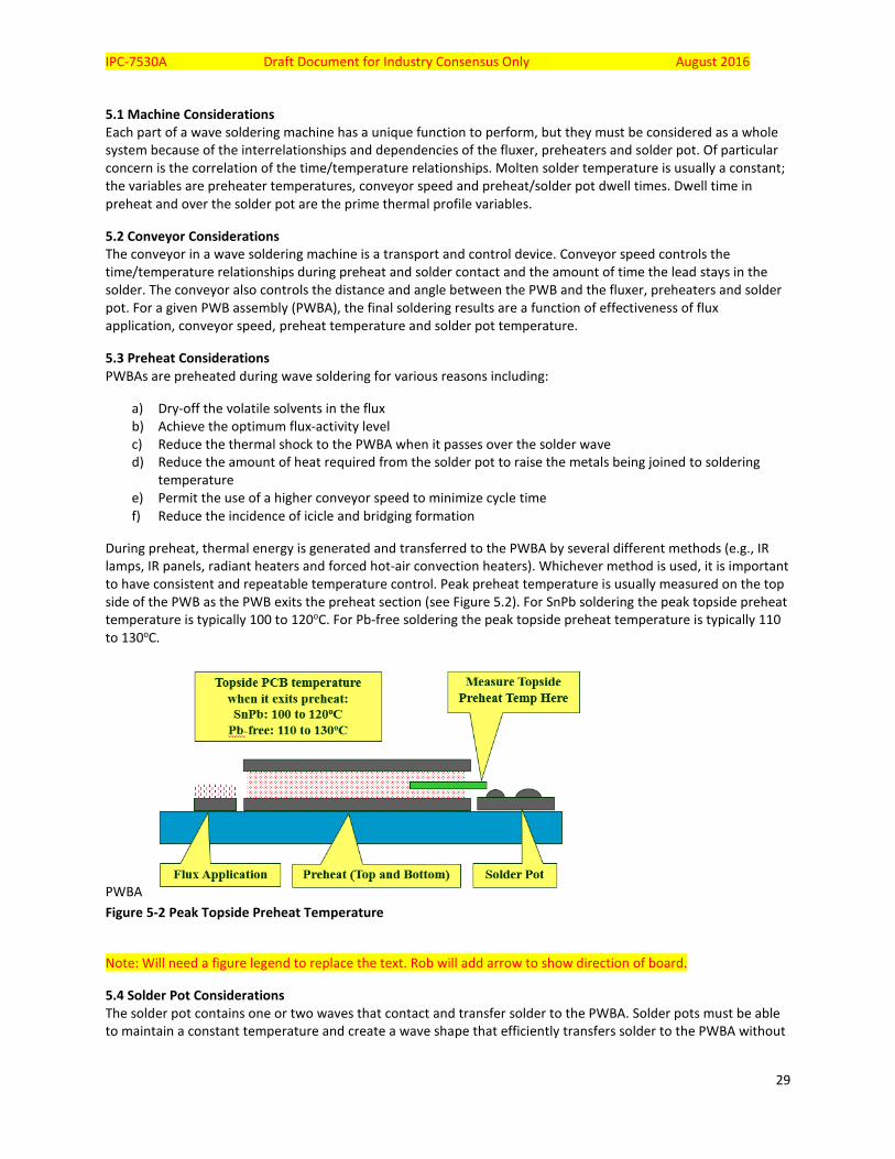
During preheat, thermal energy is generated and transferred to the PWBA by several different methods (e.g., IR lamps, IR panels, radiant heaters and forced hot-air convection heaters). Whichever method is used, it is important to have consistent and repeatable temperature control. Peak preheat temperature is usually measured on the top side of the PWB as the PWB exits the preheat section (see Figure 5.2). For SnPb soldering the peak topside preheat temperature is typically 100 to 120oC. For Pb-free soldering the peak topside preheat temperature is typically 110 to 130oC.
PWBA Figure 5-2 Peak Topside Preheat Temperature
Note: Will need a figure legend to replace the text. Rob will add arrow to show direction of board.
5.4 Solder Pot Considerations The solder pot contains one or two waves that contact and transfer solder to the PWBA. Solder pots must be able to maintain a constant temperature and create a wave shape that efficiently transfers solder to the PWBA without
IPC-7530A Draft Document for Industry Consensus Only August 2016
30
creating defects (e.g., bridging, icicles or opens). Wave shape and width are important variables to keep in mind when creating a thermal profile because they influence defects such as icicles and bridging and to some extent dwell time, which is also determined by the conveyor speed.
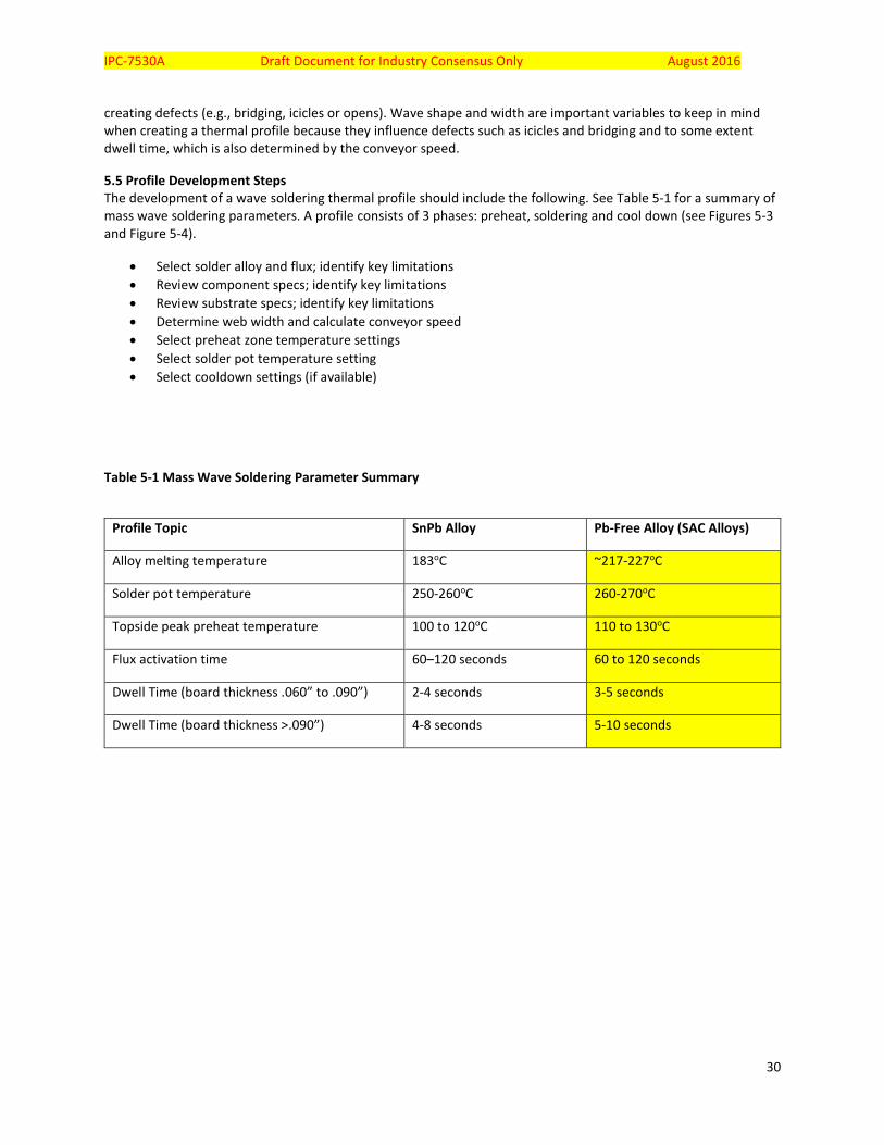
5.5 Profile Development Steps The development of a wave soldering thermal profile should include the following. See Table 5-1 for a summary of mass wave soldering parameters. A profile consists of 3 phases: preheat, soldering and cool down (see Figures 5-3 and Figure 5-4).
• Select solder alloy and flux; identify key limitations • Review component specs; identify key limitations • Review substrate specs; identify key limitations • Determine web width and calculate conveyor speed • Select preheat zone temperature settings • Select solder pot temperature setting • Select cooldown settings (if available)
Table 5-1 Mass Wave Soldering Parameter Summary
Profile Topic SnPb Alloy Pb-Free Alloy (SAC Alloys)
Alloy melting temperature 183oC ~217-227oC
Solder pot temperature 250-260oC 260-270oC
Topside peak preheat temperature 100 to 120oC 110 to 130oC
Flux activation time 60–120 seconds 60 to 120 seconds
Dwell Time (board thickness .060” to .090”) 2-4 seconds 3-5 seconds
Dwell Time (board thickness >.090”) 4-8 seconds 5-10 seconds

IPC-7530A Draft Document for Industry Consensus Only August 2016
31
Figure 5-3 Mass Wave Soldering Thermal Profile Illustration for a Single Wave Solder Pot
Figure 5-4 Mass Wave Soldering Thermal Profile Illustration for a Dual Wave Solder Pot
5.7 Design for Mass Wave Soldering Considerations The design of the PWBA is a critical factor that affects the solderability, reliability and quality of the soldered PWBA. For successful mass wave soldering, the following should be carefully considered:
a) Ratio of the size of a printed board hole to the diameter of a through-hole lead (IPC 2222) b) Distance from solder connections to the edge of a PWB c) Rigidity of the PWB at peak soldering temperature d) Retention of large components (e.g., connectors, sockets, etc.) to prevent movement during soldering e) Thermal relief of large metal planes (e.g., ground planes) to minimize “heat-sinking” effects f) Adequate clearance for proper solder wetting when using selective wave solder pallets
For wave soldering of surface mount components glued to the bottom of the board, it is necessary to align them parallel to the wave to prevent solder skips.
In selective pallet wave soldering of through-hole components, when surface mount components are reflow soldered on both top and bottom sides, adequate space is necessary between surface mount and through-hole
IPC-7530A Draft Document for Industry Consensus Only August 2016
32
components. This space allows the wave fixture to hide surface mount components from the wave while selectively soldering through-hole components.
6 SELECTIVE SOLDERING PROFILING
6.1 Solder Pot By definition, selective soldering implies creating multiple solder connections sequentially or in mass in a semi-automated or automated process.
Equipment designed for this task generally has four basic characteristics:
• PWB conveyance (if PWB moves)
• Pot and fluxer conveyance (if PWB is stationary)
• Fluxing capability
• Preheating capability
• Molten pot of solder with a single nozzle (sequential soldering)
• Molten pot of solder with a nozzle fixture (mass soldering)
The differences between manufacturers are in the application of these basic concepts and the equipment controls. Each machine has unique characteristics that need to be taken into account when developing a thermal profile.
Sequential selective soldering machines solder through-hole components in a sequence. The advantage of sequential selective soldering is that PWBs with bottom-side surface mount components can have through-hole components soldered without PWB fixturing and masking. The disadvantage is speed because the process uses sequential soldering instead of mass soldering (i.e. wave soldering).
Mass selective soldering machines solder through-hole components simultaneously using a custom nozzle fixture. The advantage of mass selective soldering is that PWBs with bottom-side surface mount components can have through-hole components soldered without PWB fixturing and masking. The disadvantage is the need for a custom nozzle fixture for each PWB. The selective soldering system automatically performs the soldering process, which is flux application, preheating of the area to be soldered, application of molten solder and solidification. All of these characteristics act together to ensure proper soldering. A solder recipe is developed by recording the optimum process parameters selected for conveyance speed, flux application, preheaters and solder temperature.
6.1.2 Machine Considerations Each part of a selective soldering machine has a unique function to perform but they must be considered as a whole system because of the interrelationships and dependencies of the fluxer, preheaters, nozzles and solder pot. Of particular concern is the correlation of the time/temperature/volume relationships. The molten solder temperature is usually a constant; the variables are preheater temperatures, preheat/solder pot dwell times and volume of solder over the nozzle. Dwell time in preheat and over the solder pot are the prime thermal profile variables.
6.1.3 Preheat Considerations PWBAs are preheated during selective soldering for various reasons. These include:
IPC-7530A Draft Document for Industry Consensus Only August 2016
33
a) Dry-off the volatile solvents in the flux b) Achieve optimum flux-activity level c) Reduce the thermal shock to the PWBA during soldering d) PWBA e) Reduce the amount of heat required from the solder pot to raise the metals being joined to soldering
temperature f) Permit the use of a higher conveyance speeds to minimize cycle time g) Reduce the incidence of icicle and bridging formation
During preheat thermal energy is generated and transferred to the PWBA by several different methods (e.g., IR lamps, IR panels, radiant heaters and forced hot-air convection heaters). Whichever method is used, it is important to have consistent and repeatable temperature control. The best control of preheat will be with machines that have closed loop control. Peak preheat temperature is usually measured on the top side of the PWB before soldering begins. For SnPb soldering the peak topside preheat temperature is typically 100 to 120oC. For Pb-free soldering the peak topside preheat temperature is typically 110 to 130oC.
6.1.4 Solder Pot and Nozzle Considerations Solder pots use a nozzle to transfer solder to the PWBA, so solder pots must maintain constant temperatures and pump speeds to efficiently transfer the solder to the PWBA without creating defects (e.g. bridging, icicles or opens). Different nozzle sizes can be used depending on the clearance the nozzle has to adjacent components. Some nozzles can create different solder wave shapes. Increasing or decreasing the pump speed can also change the shape and height of the solder wave over the nozzle.
Solder pot temperature for SnPb and lead-free may vary depending on the design of the selective soldering machine. Some suppliers recommend using a pot temperature higher than what is typically used for wave soldering because the solder volume coming in contact with the PWB is considerably smaller than in wave soldering. The molten solder temperature may be a few degrees higher than wave soldering or 20 to 30oC higher than wave soldering.
For selective soldering, a temperature of 270 °C is preferable to 290 °C (255 °C to 270 °C for wave soldering) to minimize oxidation in the solder pot. However, if the system comes with a nitrogen inerting option, 290 °C is acceptable.
6.1.5 Profile Development Steps The development of a selective soldering thermal profile should include the following. See Table 6-1 for a summary of selective soldering parameters. A profile consists of 3 phases: preheat, soldering and cool down (see Figure 6-1).
• Select solder alloy and flux; identify key limitations • Review component specs; identify key limitations • Review substrate specs; identify key limitations • Determine conveyance speed (machine or PWB) • Select preheat zone temperature settings • Select solder pot temperature setting • Select cool down settings
Table 6-1 Selective Soldering Parameter Summary
Profile Topic SnPb Alloy Pb-Free Alloy
Alloy melting temperature 183 °C ~217 °C (SAC 305), 227 °C
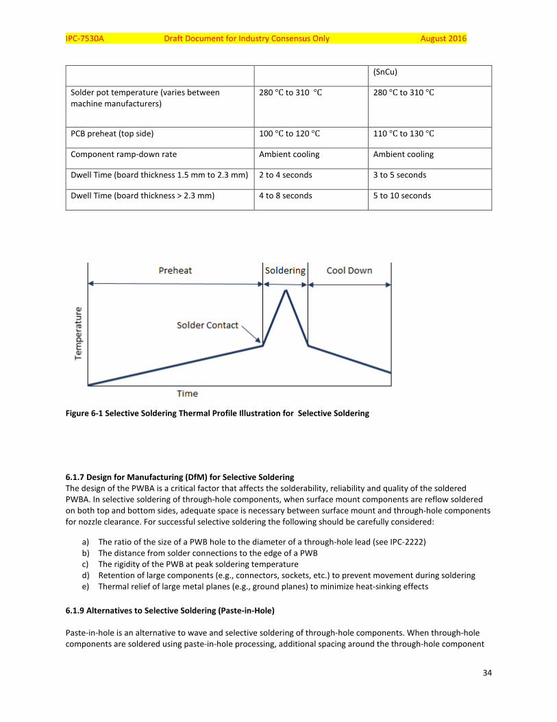
IPC-7530A Draft Document for Industry Consensus Only August 2016
34
(SnCu)
Solder pot temperature (varies between machine manufacturers)
280 °C to 310 °C
280 °C to 310 °C
PCB preheat (top side) 100 °C to 120 °C 110 °C to 130 °C
Component ramp-down rate Ambient cooling Ambient cooling
Dwell Time (board thickness 1.5 mm to 2.3 mm) 2 to 4 seconds 3 to 5 seconds
Dwell Time (board thickness > 2.3 mm) 4 to 8 seconds 5 to 10 seconds
Figure 6-1 Selective Soldering Thermal Profile Illustration for Selective Soldering
6.1.7 Design for Manufacturing (DfM) for Selective Soldering The design of the PWBA is a critical factor that affects the solderability, reliability and quality of the soldered PWBA. In selective soldering of through-hole components, when surface mount components are reflow soldered on both top and bottom sides, adequate space is necessary between surface mount and through-hole components for nozzle clearance. For successful selective soldering the following should be carefully considered:
a) The ratio of the size of a PWB hole to the diameter of a through-hole lead (see IPC-2222) b) The distance from solder connections to the edge of a PWB c) The rigidity of the PWB at peak soldering temperature d) Retention of large components (e.g., connectors, sockets, etc.) to prevent movement during soldering e) Thermal relief of large metal planes (e.g., ground planes) to minimize heat-sinking effects
6.1.9 Alternatives to Selective Soldering (Paste-in-Hole) Paste-in-hole is an alternative to wave and selective soldering of through-hole components. When through-hole components are soldered using paste-in-hole processing, additional spacing around the through-hole component
IPC-7530A Draft Document for Industry Consensus Only August 2016
35
is necessary to allow desired volume of solder paste around the through-hole pads to achieve 100 % solder fillets. In addition, it is important to allow the right gap between the lead and the hole. For example, the plated through-hole (PTH) diameter should be about 3mm larger than the lead diameter to allow capillary action to fill solder in the PTH. If the gap is too large, paste-in-hole processing may not provide acceptable solder fillets.
6.2 Alternatives to Selective Soldering (Laser) Laser soldering is performed at a very high temperature for a very short time. For through-hole leads, the time for each solder joint is about one second. There are laser soldering systems that require a half a second or even less per joint for selective soldering of surface mount leads.
The lasers solder exposed solder joints such as the leads of through-hole and gull wing devices but also to solder hidden solder joints of packages such as BGAs and micro BGAs.
In laser soldering, the solder for though-hole components is applied as wire and as solder paste by dispending or printing for surface mount components. For surface mount components, solder paste is dispensed or printed.
Since soldering time in laser soldering is very short (as short as quarter of a second), the potential for formation of solder balls is very high when using solder paste. It is very important to find paste supplier who can formulate paste specifically for laser soldering.
Laser soldering uses diode lasers to heat the component lead and PTH pad while automatically feeding solder wire to achieve the desired fillet. The wire has flux inside its core.
Laser soldering for through-hole components is a point-to-point soldering process similar to hand soldering, but it is faster and produces consistent quality, a key concern in hand soldering. Another laser soldering benefit, transitions from tin/lead to lead-free take minutes, requiring only that operators replace the solder wire spool.
The key elements of a laser solder profile are laser power that varies from 20 watts to 100 watts, soldering time that can vary from 200 milliseconds to 4 to 5 minutes for large BGAs with hidden solder joints under the package. Heat is applied by laser in a defocused manner, and the entire package is heated, thus transferring the heat to the balls (i.e., as is the case in hot-air soldering). Use of preheat is highly recommended to achieve better solder joints in shorter time.
7 TEMPERATURE PROFILING TOOLS
7.1 Product Profilers A product thermal profiler, also called remote pass-through thermal profiler, is a hardware/software kit that can travel with the Printed Wiring Board through the soldering equipment, and that records the temperatures measured by temperature sensors affixed to the PWB. Temperature sensors are attached to the thermal profiler, the thermal profiler is inserted into a thermal barrier to protect it from the process temperatures, and is mounted to the PCB using a carrier. After the run, the temperature data/profile can be downloaded to PC for analysis. Figure 7-1 shows an example for a thermal profiler kit with the profiler, thermocouples, a thermal barrier and a carrier.
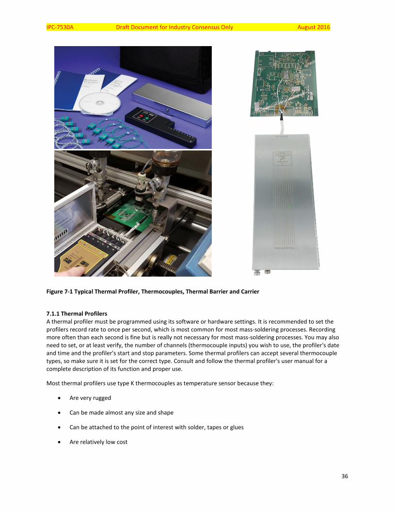
IPC-7530A Draft Document for Industry Consensus Only August 2016
36
Figure 7-1 Typical Thermal Profiler, Thermocouples, Thermal Barrier and Carrier
7.1.1 Thermal Profilers A thermal profiler must be programmed using its software or hardware settings. It is recommended to set the profilers record rate to once per second, which is most common for most mass-soldering processes. Recording more often than each second is fine but is really not necessary for most mass-soldering processes. You may also need to set, or at least verify, the number of channels (thermocouple inputs) you wish to use, the profiler's date and time and the profiler's start and stop parameters. Some thermal profilers can accept several thermocouple types, so make sure it is set for the correct type. Consult and follow the thermal profiler's user manual for a complete description of its function and proper use.
Most thermal profilers use type K thermocouples as temperature sensor because they:
• Are very rugged
• Can be made almost any size and shape
• Can be attached to the point of interest with solder, tapes or glues
• Are relatively low cost
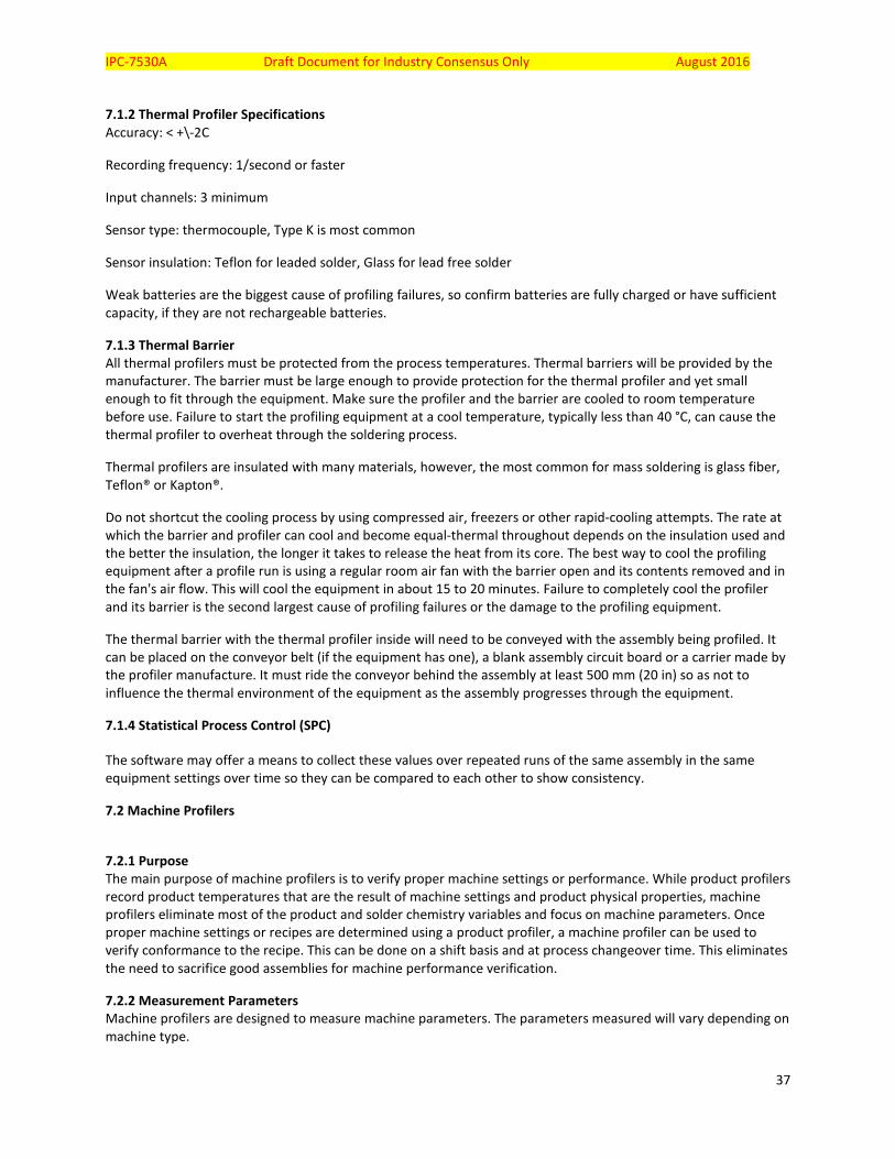
IPC-7530A Draft Document for Industry Consensus Only August 2016
37
7.1.2 Thermal Profiler Specifications Accuracy: < +\-2C
Recording frequency: 1/second or faster
Input channels: 3 minimum
Sensor type: thermocouple, Type K is most common
Sensor insulation: Teflon for leaded solder, Glass for lead free solder
Weak batteries are the biggest cause of profiling failures, so confirm batteries are fully charged or have sufficient capacity, if they are not rechargeable batteries.
7.1.3 Thermal Barrier All thermal profilers must be protected from the process temperatures. Thermal barriers will be provided by the manufacturer. The barrier must be large enough to provide protection for the thermal profiler and yet small enough to fit through the equipment. Make sure the profiler and the barrier are cooled to room temperature before use. Failure to start the profiling equipment at a cool temperature, typically less than 40 °C, can cause the thermal profiler to overheat through the soldering process.
Thermal profilers are insulated with many materials, however, the most common for mass soldering is glass fiber, Teflon® or Kapton®.
Do not shortcut the cooling process by using compressed air, freezers or other rapid-cooling attempts. The rate at which the barrier and profiler can cool and become equal-thermal throughout depends on the insulation used and the better the insulation, the longer it takes to release the heat from its core. The best way to cool the profiling equipment after a profile run is using a regular room air fan with the barrier open and its contents removed and in the fan's air flow. This will cool the equipment in about 15 to 20 minutes. Failure to completely cool the profiler and its barrier is the second largest cause of profiling failures or the damage to the profiling equipment.
The thermal barrier with the thermal profiler inside will need to be conveyed with the assembly being profiled. It can be placed on the conveyor belt (if the equipment has one), a blank assembly circuit board or a carrier made by the profiler manufacture. It must ride the conveyor behind the assembly at least 500 mm (20 in) so as not to influence the thermal environment of the equipment as the assembly progresses through the equipment.
7.1.4 Statistical Process Control (SPC) The software may offer a means to collect these values over repeated runs of the same assembly in the same equipment settings over time so they can be compared to each other to show consistency.
7.2 Machine Profilers
7.2.1 Purpose The main purpose of machine profilers is to verify proper machine settings or performance. While product profilers record product temperatures that are the result of machine settings and product physical properties, machine profilers eliminate most of the product and solder chemistry variables and focus on machine parameters. Once proper machine settings or recipes are determined using a product profiler, a machine profiler can be used to verify conformance to the recipe. This can be done on a shift basis and at process changeover time. This eliminates the need to sacrifice good assemblies for machine performance verification.
7.2.2 Measurement Parameters Machine profilers are designed to measure machine parameters. The parameters measured will vary depending on machine type.

IPC-7530A Draft Document for Industry Consensus Only August 2016
38
Reflow oven profilers may record conveyor speeds, zone sizes, zone air temperatures or heat flow. Heat flow is the product of zone temperature and air flow or the ability of the oven to deliver heat to the assembly. Some machine profiling equipment measures airflow in the oven or even ultraviolet (UV) and IR radiation.
Wave solder profilers record conveyor speeds, preheat temperatures and a number of chip and main solder wave parameters. Wave parameters may include contact length, wave height, wave parallelism, wave temperature and change in temperature at the wave. Wave machine profilers may also measure top- and bottom-side board temperatures as measured on a coupon designed to simulate a typical circuit board. Some wave solder machine profilers can provide a digitized representation of the contact area between the board and the wave.
7.2.3 Machine Verification Thermal profiling must be performed on equipment that has been first verified for proper function. The equipment must be first powered and set to the desired settings and allowed to reach thermal stability. Most equipment can inform the operator when it has reached its settings. In general, this will take 20 to 30 minutes. Do not attempt to short cut this process by forced venting of heat or altering the equipment’s acceptable limits. Give the equipment enough time to reach thermal stability.
Verification of the equipment's function is typically done using thermally stable materials that have been instrumented with thermocouples and passed through the equipment, in the same manner as an assembly, to verify the equipment produces the same thermal profile. There are several commercially available verification tools specifically designed to preform equipment verification. Or you may develop your own using thermally stable materials like aluminum, stainless steel or titanium, machined into plates or blocks suspended in a fixture or pallet which allows some thermal isolation between measurements points. Thermocouples should be permanently attached by welding, brazing or mechanically securing into the core of or onto the surface of the plate or block. Two mm to 4 mm thick material typically will produce verification profile zone values similar to assemble profiles. Thicker materials may not reach the same temperatures as assembly profiles, but can be equally as useful for equipment verification profiles. Measurement points must cover the width of the conveyor in at least three locations evenly spaced across the conveyor width. Clearly, the equipment being verified, whether reflow, wave, selective, vapor phase, or rework, to name a few, will dictate the basic shape and of the verification fixture and the number of measurement points. All must be able to withstand the process temperatures and cover the processing area of the equipment. It does not matter the exact shape or size of this fixture provided it fits the equipment, can withstand the temperatures and you use it in a consistent and repeatable manor.
Verification must be done using the same equipment settings as the previous verification. These settings may be specific set used only for this equipment verification profile or the same settings you plan to use for a specific assembly. It does not matter, so long as you have a previous verification profile at these settings for comparison, unless this is the first verification at these equipment settings. Using the same settings you plan to use for an assembly profile will save time since you do not need to wait for the equipment to reach two different settings: once for the verification profile and again for the assembly profile.
The equipment settings used for verification should include the measurement values from the same profile zones used for the desired assembly profile. For reflow these zones include:
Preheat - slope to a temperature
Soak - time between the end of the preheat and the liquidus temperature
Reflow - time above the liquidus temperature
Cooling - slope from peak temperature and the liquidus temperature
Verifying that the values for each of these profile zones are consistent with the previous verification profile will confirm the equipment is consistent and ready to profile the assembly or run production. Additional values may be taken from the verification profile depending on the process or equipment type.
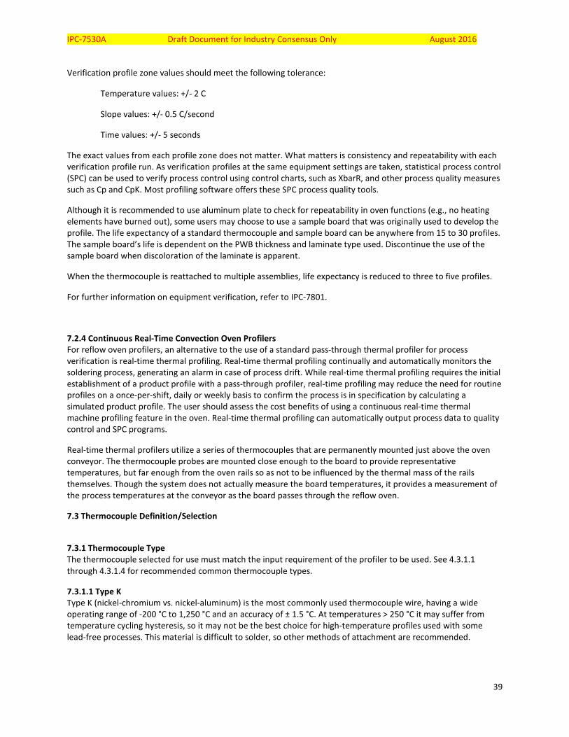
IPC-7530A Draft Document for Industry Consensus Only August 2016
39
Verification profile zone values should meet the following tolerance:
Temperature values: +/- 2 C
Slope values: +/- 0.5 C/second
Time values: +/- 5 seconds
The exact values from each profile zone does not matter. What matters is consistency and repeatability with each verification profile run. As verification profiles at the same equipment settings are taken, statistical process control (SPC) can be used to verify process control using control charts, such as XbarR, and other process quality measures such as Cp and CpK. Most profiling software offers these SPC process quality tools.
Although it is recommended to use aluminum plate to check for repeatability in oven functions (e.g., no heating elements have burned out), some users may choose to use a sample board that was originally used to develop the profile. The life expectancy of a standard thermocouple and sample board can be anywhere from 15 to 30 profiles. The sample board’s life is dependent on the PWB thickness and laminate type used. Discontinue the use of the sample board when discoloration of the laminate is apparent.
When the thermocouple is reattached to multiple assemblies, life expectancy is reduced to three to five profiles.
For further information on equipment verification, refer to IPC-7801.
7.2.4 Continuous Real-Time Convection Oven Profilers For reflow oven profilers, an alternative to the use of a standard pass-through thermal profiler for process verification is real-time thermal profiling. Real-time thermal profiling continually and automatically monitors the soldering process, generating an alarm in case of process drift. While real-time thermal profiling requires the initial establishment of a product profile with a pass-through profiler, real-time profiling may reduce the need for routine profiles on a once-per-shift, daily or weekly basis to confirm the process is in specification by calculating a simulated product profile. The user should assess the cost benefits of using a continuous real-time thermal machine profiling feature in the oven. Real-time thermal profiling can automatically output process data to quality control and SPC programs.
Real-time thermal profilers utilize a series of thermocouples that are permanently mounted just above the oven conveyor. The thermocouple probes are mounted close enough to the board to provide representative temperatures, but far enough from the oven rails so as not to be influenced by the thermal mass of the rails themselves. Though the system does not actually measure the board temperatures, it provides a measurement of the process temperatures at the conveyor as the board passes through the reflow oven.
7.3 Thermocouple Definition/Selection
7.3.1 Thermocouple Type The thermocouple selected for use must match the input requirement of the profiler to be used. See 4.3.1.1 through 4.3.1.4 for recommended common thermocouple types.
7.3.1.1 Type K Type K (nickel-chromium vs. nickel-aluminum) is the most commonly used thermocouple wire, having a wide operating range of -200 °C to 1,250 °C and an accuracy of ± 1.5 °C. At temperatures > 250 °C it may suffer from temperature cycling hysteresis, so it may not be the best choice for high-temperature profiles used with some lead-free processes. This material is difficult to solder, so other methods of attachment are recommended.
IPC-7530A Draft Document for Industry Consensus Only August 2016
40
7.3.1.2 Type T Type T (copper vs. copper-nickel) has an operating range of -200 °C to 350 °C and good solderability, making it easy to attach by soldering. The copper arm has high thermal conductivity, so thinner wire gauges are preferred. It has an accuracy of ± 0.5 °C.
7.3.1.3 Type J Type J (iron vs. copper-nickel) has an operating range from 0 °C to 750 °C and an accuracy of ± 1.5 °C. This material is difficult to solder, so other methods of attachment are recommended. It is prone to rusting in humid atmospheres, which will shorten its working life.
7.3.1.4 Type N Type N (nickel-14.2 % chromium-1.4 % silicon vs. nickel-4.4 % silicon-0.1 % magnesium) has an operating range of - 270 °C to 1300 °C. This material is difficult to solder, so other methods of attachment are recommended. It is one of the most stable thermocouple materials and is available with an accuracy of ± 1.1 °C or 0.4%.
7.3.2 Thermocouple Wire Gauge The most commonly used wire for profiling is 36 AWG. 38 AWG may offer greater sensitivity, but it is more fragile and will have a shorter operational life. 34 AWG offers greater operational life, but it may affect the temperature of the measurement site by conducting heat into or from the thermocouple wire.
7.3.3 Insulation Insulation of the thermocouple is dependent on the environment and temperature extremes to which it will be exposed. For most soldering applications, glass-braid insulation is used.
Note: Glass braid offers good high-temperature stability, but it has poor flexibility which may make handling more difficult. Polytetrafluoroethylene (PTFE) offers better flexibility, but will degrade more quickly with repeated heat cycles.
7.3.4 Wire Length It is recommended that thermocouple lengths not exceed approximately 1 m (36 in). Long thermocouple wires can introduce measurement error; the thermocouple wire should be as short as practical to reduce the effects of noise and resistance and to prevent mechanical damage.
7.4 Thermocouple Junction The formation of the thermocouple should be a welded junction. It is recommended that whenever the original junction weld is broken the thermocouple be replaced. In the event that the weld or a wire is broken, one should never consider twisting the thermocouple wires together to form a junction. This can result in an incorrect temperature measurement.
7.5 Calibration and Test Calibration of the data logger should be performed as required by the OEM or in accordance to the equipment manufacturer specifications. In the absence of OEM or manufacturer’s recommendation, calibration and testing every six months of operation may be established. A noncalibrated data logger should never be used.
Thermocouples should be verified for proper operation whenever they have been used more than once. This can be achieved by comparing temperature measurements of the used thermocouple to a calibrated thermocouple with the use of a calibrated data logger.
7.6 Thermocouple Attachment
7.6.1 High-Temperature Solder High temperature solder attachment should be considered for a sample board that will be profiled multiple times.
IPC-7530A Draft Document for Industry Consensus Only August 2016
41
It provides a consistent reproducible thermal connection. Figure 7-2 shows attachment of a thermocouple using solder. Care should be taken not to use high temperature solder attachment too close to the melting point of the solder.
Figure 7-2 Thermocouple Attachment (Solder Method)
7.6.2 Adhesives There are many types of adhesives used for thermocouple attachment, all of which have different curing mechanisms (e.g., heat, air and UV). Whichever type of adhesive is used, it is important that it is thermally conductive. More information about thermally conductive adhesive can be obtained from IPC-CA-821, General Requirements for Thermally Conductive Adhesives. This method of attachment should be considered for a sample board and will be profiled multiple times, but the process temperatures are too high for high temperature solder. Attachment of a thermocouple using adhesive is shown in Figure 7-3.
Figure 7-3 Thermocouple Attachment (Adhesive Method)
7.6.3 Aluminum/Copper Tape Aluminum/copper tape provides a securely connected thermocouple with good thermal conductivity, is nondestructive and leaves no scars or residuals. Using aluminum/copper tape reduces the amount of effort and
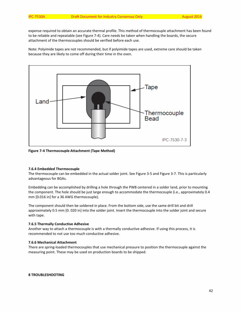
IPC-7530A Draft Document for Industry Consensus Only August 2016
42
expense required to obtain an accurate thermal profile. This method of thermocouple attachment has been found to be reliable and repeatable (see Figure 7-4). Care needs be taken when handling the boards, the secure attachment of the thermocouples should be verified before each use.
Note: Polyimide tapes are not recommended, but if polyimide tapes are used, extreme care should be taken because they are likely to come off during their time in the oven.
Figure 7-4 Thermocouple Attachment (Tape Method)
7.6.4 Embedded Thermocouple The thermocouple can be embedded in the actual solder joint. See Figure 3-5 and Figure 3-7. This is particularly advantageous for BGAs.
Embedding can be accomplished by drilling a hole through the PWB centered in a solder land, prior to mounting the component. The hole should be just large enough to accommodate the thermocouple (i.e., approximately 0.4 mm [0.016 in] for a 36 AWG thermocouple).
The component should then be soldered in place. From the bottom side, use the same drill bit and drill approximately 0.5 mm [0. 020 in] into the solder joint. Insert the thermocouple into the solder joint and secure with tape.
7.6.5 Thermally Conductive Adhesive Another way to attach a thermocouple is with a thermally conductive adhesive. If using this process, it is recommended to not use too much conductive adhesive.
7.6.6 Mechanical Attachment There are spring-loaded thermocouples that use mechanical pressure to position the thermocouple against the measuring point. These may be used on production boards to be shipped.
8 TROUBLESHOOTING
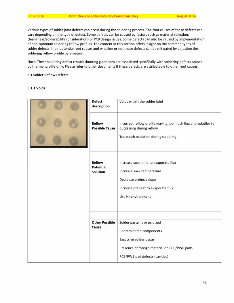
IPC-7530A Draft Document for Industry Consensus Only August 2016
43
Various types of solder joint defects can occur during the soldering process. The root causes of these defects can vary depending on the type of defect. Some defects can be caused by factors such as material selection, cleanliness/solderability considerations or PCB design issues. Some defects can also be caused by implementation of non-optimum soldering reflow profiles. The content in this section offers insight on the common types of solder defects, their potential root causes and whether or not these defects can be mitigated by adjusting the soldering reflow profile parameters.
Note: These soldering defect troubleshooting guidelines are associated specifically with soldering defects caused by thermal profile only. Please refer to other documents if these defects are attributable to other root causes.
8.1 Solder Reflow Defects
8.1.1 Voids
Defect description
Voids within the solder joint
Reflow Possible Cause
Incorrect reflow profile leaving too much flux and volatiles to outgassing during reflow
Too much oxidation during soldering
Reflow Potential Solution
Increase soak time to evaporate flux
Increase soak temperature
Decrease preheat slope
Increase preheat to evaporate flux
Use N2 environment
Other Possible Cause
Solder paste have oxidized
Contaminated components
Excessive solder paste
Presence of foreign material on PCB/PWB pads
PCB/PWB pad defects (cavities)
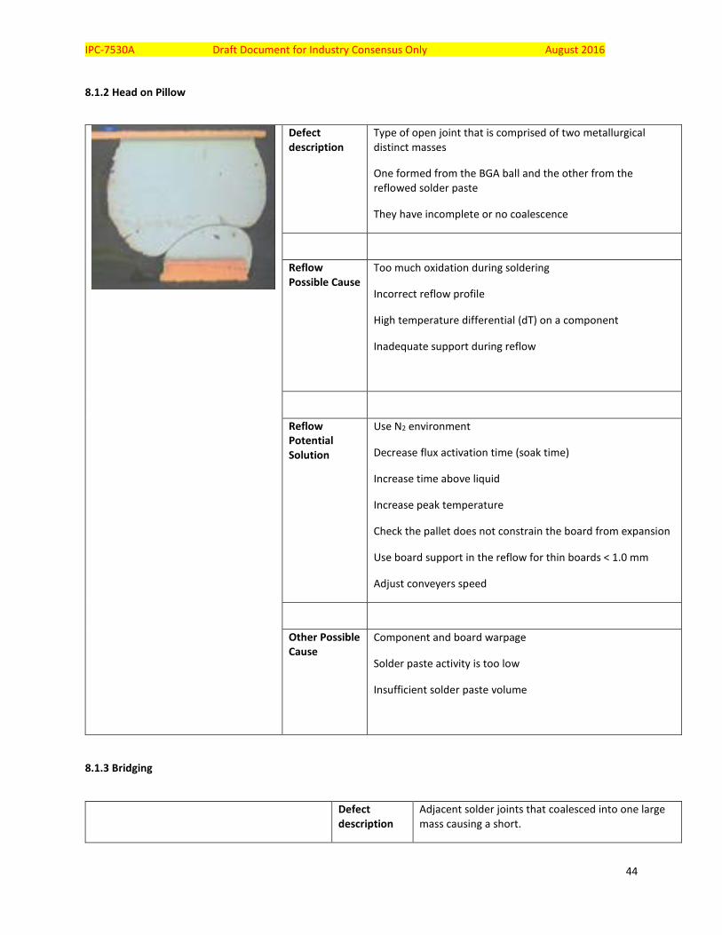
IPC-7530A Draft Document for Industry Consensus Only August 2016
44
8.1.2 Head on Pillow
Defect description
Type of open joint that is comprised of two metallurgical distinct masses
One formed from the BGA ball and the other from the reflowed solder paste
They have incomplete or no coalescence
Reflow Possible Cause
Too much oxidation during soldering
Incorrect reflow profile
High temperature differential (dT) on a component
Inadequate support during reflow
Reflow Potential Solution
Use N2 environment
Decrease flux activation time (soak time)
Increase time above liquid
Increase peak temperature
Check the pallet does not constrain the board from expansion
Use board support in the reflow for thin boards < 1.0 mm
Adjust conveyers speed
Other Possible Cause
Component and board warpage
Solder paste activity is too low
Insufficient solder paste volume
8.1.3 Bridging
Defect description
Adjacent solder joints that coalesced into one large mass causing a short.
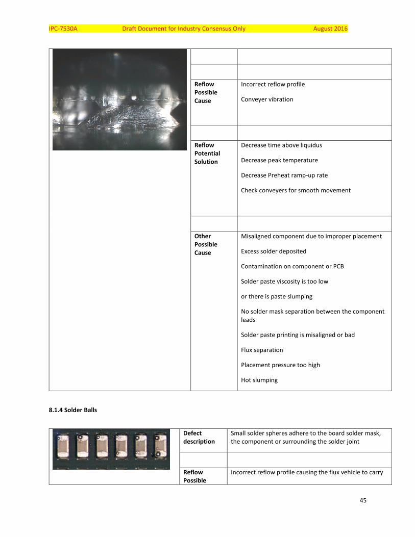
IPC-7530A Draft Document for Industry Consensus Only August 2016
45
Reflow Possible Cause
Incorrect reflow profile
Conveyer vibration
Reflow Potential Solution
Decrease time above liquidus
Decrease peak temperature
Decrease Preheat ramp-up rate
Check conveyers for smooth movement
Other Possible Cause
Misaligned component due to improper placement
Excess solder deposited
Contamination on component or PCB
Solder paste viscosity is too low
or there is paste slumping
No solder mask separation between the component leads
Solder paste printing is misaligned or bad
Flux separation
Placement pressure too high
Hot slumping
8.1.4 Solder Balls
Defect description
Small solder spheres adhere to the board solder mask, the component or surrounding the solder joint
Reflow Possible
Incorrect reflow profile causing the flux vehicle to carry
IPC-7530A Draft Document for Industry Consensus Only August 2016
46
Cause solder particle away from the joint
Too much oxidation during soldering solder particle cannot coalesces together
Reflow Potential Solution
Increase preheat to evaporate flux
Reduce preheat ramp rate
Other Possible Cause
Solder particles in the solder paste have oxidized
Solder paste viscosity is too low resulting in slumping onto the mask
Misalignment of paste print on the solder mask
Solder paste is contaminated with oxidized particles
Solder paste misprint
Circuit boards not properly cleaned
Insufficient flux content in the solder paste
Solder paste stencils are dirty
Small solder particles
Excess pressure pushing solder paste onto the mask
Entrapped volatiles causing solder splattering
8.1.5 Cold Solder/Incomplete Solder
Defect description
Solder look grainy and incomplete.
Reflow Possible Cause
The solder did not reach the required temperature and time to create a joint
Improper oven temperatures
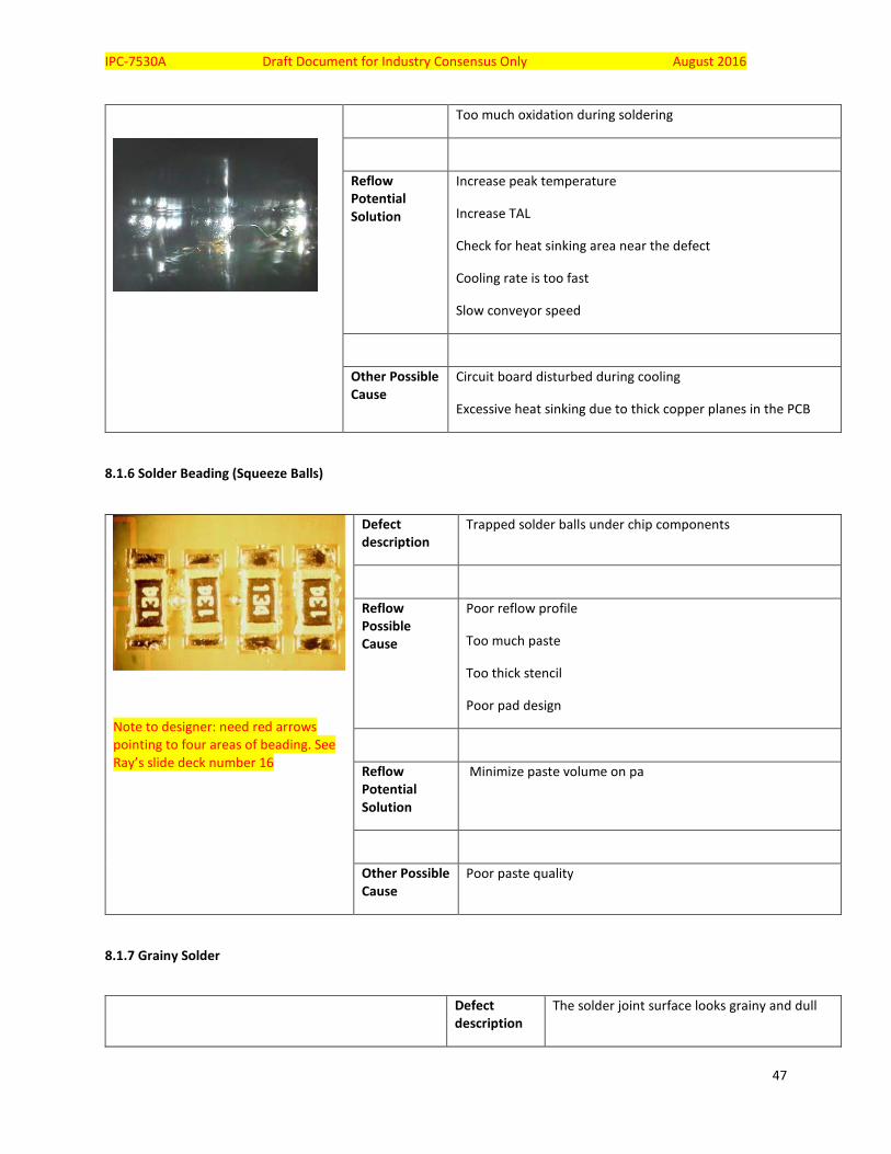
IPC-7530A Draft Document for Industry Consensus Only August 2016
47
Too much oxidation during soldering
Reflow Potential Solution
Increase peak temperature
Increase TAL
Check for heat sinking area near the defect
Cooling rate is too fast
Slow conveyor speed
Other Possible Cause
Circuit board disturbed during cooling
Excessive heat sinking due to thick copper planes in the PCB
8.1.6 Solder Beading (Squeeze Balls)
Note to designer: need red arrows pointing to four areas of beading. See Ray’s slide deck number 16
Defect description
Trapped solder balls under chip components
Reflow Possible Cause
Poor reflow profile
Too much paste
Too thick stencil
Poor pad design
Reflow Potential Solution
Minimize paste volume on pa
Other Possible Cause
Poor paste quality
8.1.7 Grainy Solder
Defect description
The solder joint surface looks grainy and dull
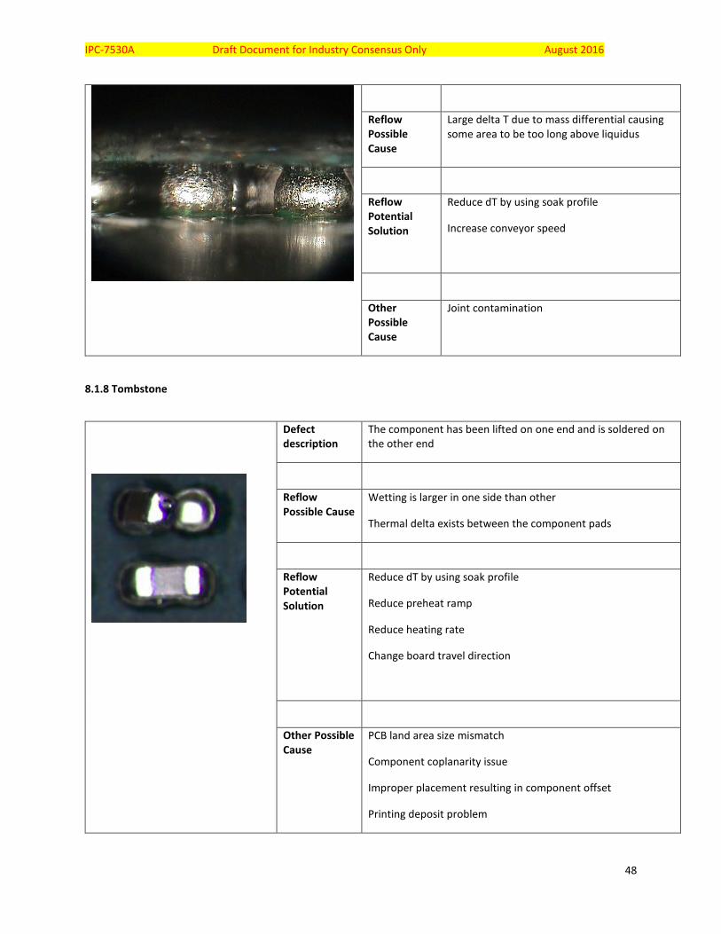
IPC-7530A Draft Document for Industry Consensus Only August 2016
48
Reflow Possible Cause
Large delta T due to mass differential causing some area to be too long above liquidus
Reflow Potential Solution
Reduce dT by using soak profile
Increase conveyor speed
Other Possible Cause
Joint contamination
8.1.8 Tombstone
Defect description
The component has been lifted on one end and is soldered on the other end
Reflow Possible Cause
Wetting is larger in one side than other
Thermal delta exists between the component pads
Reflow Potential Solution
Reduce dT by using soak profile
Reduce preheat ramp
Reduce heating rate
Change board travel direction
Other Possible Cause
PCB land area size mismatch
Component coplanarity issue
Improper placement resulting in component offset
Printing deposit problem
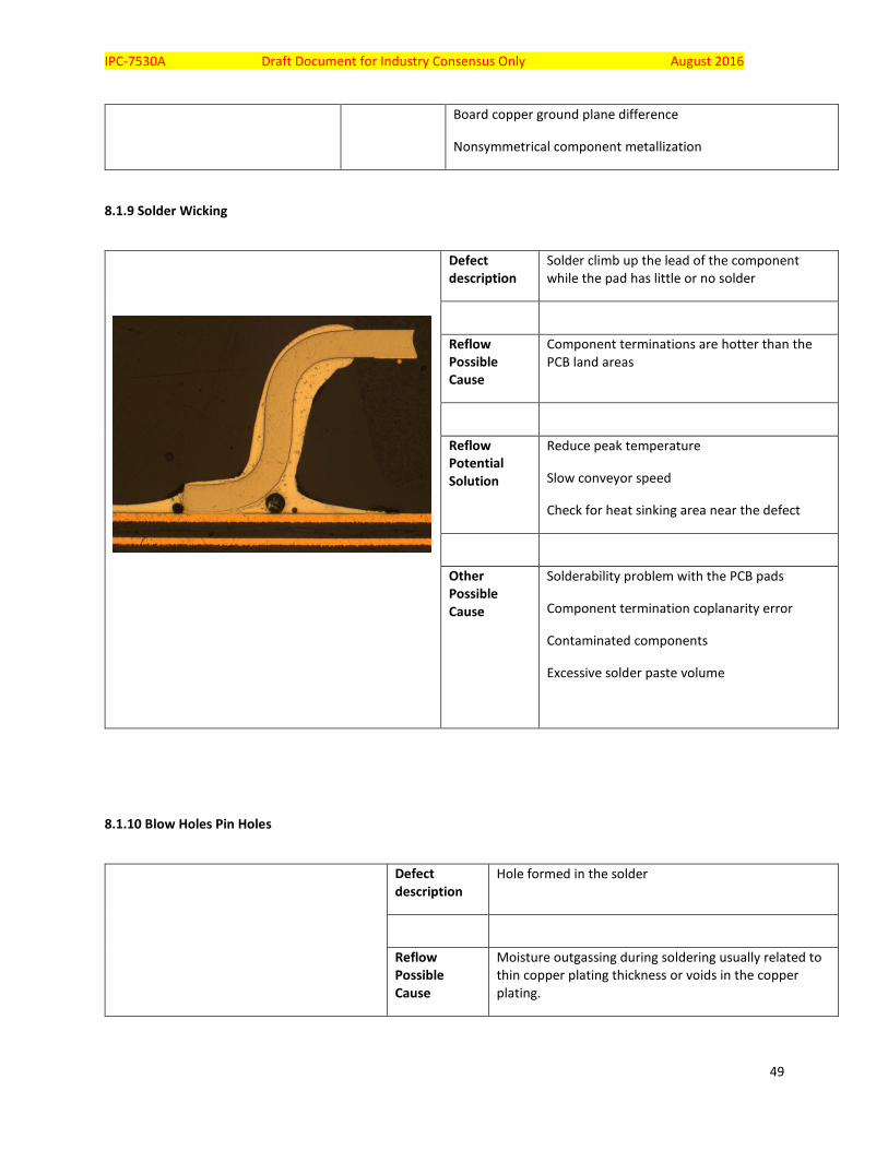
IPC-7530A Draft Document for Industry Consensus Only August 2016
49
Board copper ground plane difference
Nonsymmetrical component metallization
8.1.9 Solder Wicking
Defect description
Solder climb up the lead of the component while the pad has little or no solder
Reflow Possible Cause
Component terminations are hotter than the PCB land areas
Reflow Potential Solution
Reduce peak temperature
Slow conveyor speed
Check for heat sinking area near the defect
Other Possible Cause
Solderability problem with the PCB pads
Component termination coplanarity error
Contaminated components
Excessive solder paste volume
8.1.10 Blow Holes Pin Holes
Defect description
Hole formed in the solder
Reflow Possible Cause
Moisture outgassing during soldering usually related to thin copper plating thickness or voids in the copper plating.
IPC-7530A Draft Document for Industry Consensus Only August 2016
50
Reflow Potential Solution
Reflow temperature is too low
Preheat ramp-up rate is too high
Other Possible Cause
Contamination present
Excess volatile content in the solder paste
Table 8-1 Root Causes of Defects in Solder Joints
Type of Defect Soldering Profile Related Root Causes
Other Root Causes
Bridging 1. Preheat ramp-up rate is too high 1. Misaligned component due to improper placement 2. Excess solder deposited 3. Contamination on component or PCB 4. Solder paste viscosity is too low or there is paste slumping 5. No solder mask separation between the component leads 6. Solder paste printing is misaligned or bad 7. Flux separation 8. Placement pressure too high 9. Hot slumping
Solder Balling 1. Heating rate is too high causing evaporation of the flux. 2. Preheat ramp rate is too high. 3. Preheat temperature is too high
1. Solder particles in the solder paste have oxidized 2. Solder paste viscosity is too low resulting in slumping onto the mask 3. Misalignment of paste print on the solder mask 4. Solder paste is contaminated with oxidized particles 5. Solder paste misprint 6. Circuit boards not properly cleaned 7. Insufficient flux content in the solder paste 8. Solder paste stencils are dirty 9. Small solder particles 10. Excess pressure pushing solder paste onto the mask 11. Entrapped volatiles causing solder splattering

IPC-7530A Draft Document for Industry Consensus Only August 2016
51
Solder Beading (Squeeze Balls)
1. Not a contributor to the defect
2. <inconsistent w/ the 6.1.6>
3. Poor reflow profile 4. Too much paste 5. Too thick stencil 6. Poor pad design
1. Too much solder paste under small components
Tombstoning 1. Heating rate is too high 1. PCB land area size mismatch 2. Component coplanarity issue 3. Improper placement resulting in component offset
Wicking of Solder
1. Peak temperature is too high
2. Component terminations are hotter than the PCB land areas
1. Component terminations are hotter than the PCB land areas 2. Component termination coplanarity error 3. Contaminated components
Cold Solder Joints 1. Cooling rate is too fast 2. Peak temperature is too low 3. TAL is too low 4. Improper oven temperatures 5. Conveyor speed is too fast
1. Circuit board disturbed during cooling 2. Excessive heat sinking due to thick copper planes in the PCB
Hot Slumping 1. Preheat ramp-up rate is too high 2. Reflow cycle time is too long
1. None identified
Grainy or Large Grain Size Solder Joints
1. Cool down rate is too low. 2. Reflow temperature is too low
1. Circuit board or components contaminated
Cracked Components 1. Improper profile settings resulting in thermal shock to the components 2. reheat ramp rate is too high
1. Bad components 2. Component placement pressure is too high 3. Improper circuit board supports 4. Bad feeders/shutter jam
Cracked Solder Joints 1. Cooling rate is too fast 2. Improper profile settings resulting in thermal shock to components 3. TAL is too high or peak temperature is too high resulting in excessive IMC
1. CTE mismatch 2. Poor handling practice 3. Localized PCB warpage
Popcorn Delamination 1. Preheat ramp-up rate is too high 1. Components are absorbing
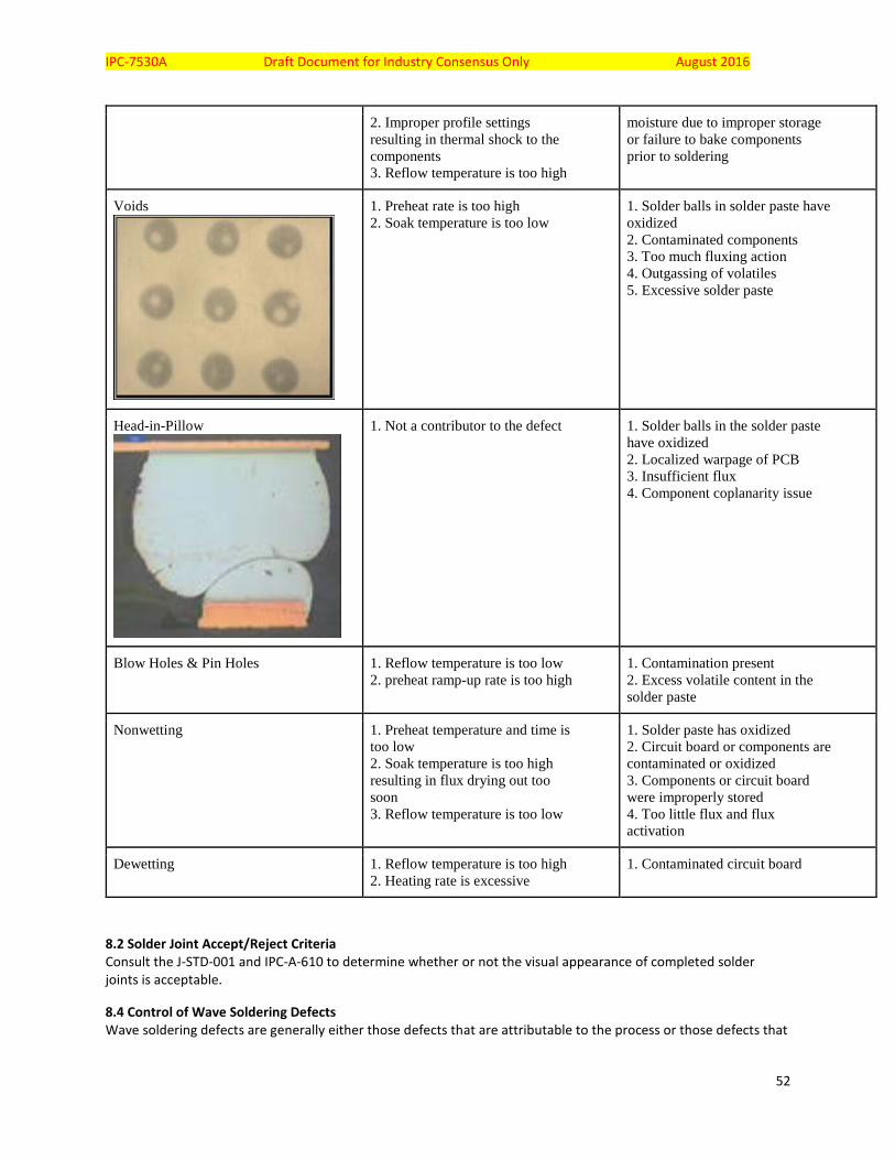
IPC-7530A Draft Document for Industry Consensus Only August 2016
52
2. Improper profile settings resulting in thermal shock to the components 3. Reflow temperature is too high
moisture due to improper storage or failure to bake components prior to soldering
Voids
1. Preheat rate is too high 2. Soak temperature is too low
1. Solder balls in solder paste have oxidized 2. Contaminated components 3. Too much fluxing action 4. Outgassing of volatiles 5. Excessive solder paste
Head-in-Pillow
1. Not a contributor to the defect 1. Solder balls in the solder paste have oxidized 2. Localized warpage of PCB 3. Insufficient flux 4. Component coplanarity issue
Blow Holes & Pin Holes 1. Reflow temperature is too low 2. preheat ramp-up rate is too high
1. Contamination present 2. Excess volatile content in the solder paste
Nonwetting 1. Preheat temperature and time is too low 2. Soak temperature is too high resulting in flux drying out too soon 3. Reflow temperature is too low
1. Solder paste has oxidized 2. Circuit board or components are contaminated or oxidized 3. Components or circuit board were improperly stored 4. Too little flux and flux activation
Dewetting 1. Reflow temperature is too high 2. Heating rate is excessive
1. Contaminated circuit board
8.2 Solder Joint Accept/Reject Criteria Consult the J-STD-001 and IPC-A-610 to determine whether or not the visual appearance of completed solder joints is acceptable.
8.4 Control of Wave Soldering Defects Wave soldering defects are generally either those defects that are attributable to the process or those defects that

IPC-7530A Draft Document for Industry Consensus Only August 2016
53
are beyond wave soldering system control (i.e., they are inherent in the components, printed boards and assembly design). Thus, with proper process control and the use of a well-designed assembly and printed boards and components with good solderability, a modern well-controlled wave soldering process will be virtually defect-free.


![de partido a su piscina… - BINDER · Tipo BGA 160 BGA 215 BGA 275 BGA 320 BGA 430 BGA 550 BGA 600 BGA 1200 Tensión de conexión [VAC] 230 230 230 230 230 230 230 230 Rango de frecuencia](https://img.pdfslide.net/doc/110x75/5c132e8509d3f26c7c8c5e0d/de-partido-a-su-piscina-binder-tipo-bga-160-bga-215-bga-275-bga-320-bga-430.jpg)