Embed Size (px)
Citation preview

ARTICLE IN PRESS
*Correspond
E-mail addr
1369-8001/$ - se
doi:10.1016/j.m
Materials Science in Semiconductor Processing 6 (2003) 277–279
Isochronal annealing study of hydrogen interaction withimplantation-induced point defects in p-type silicon
Yutaka Tokuda*, Hisanori Sato
Department of Electronics, Aichi Institute of Technology, Yakusa, Toyota 470-0392, Japan
Abstract
Isochronal annealing with zero and reverse bias applied to Schottky diodes was used to monitor the evolution of
hydrogen interaction with point defects observed in hydrogen-implanted p-type silicon, i.e., divacancy (VV), carbon–
oxygen interstitial pair (CiOi) and two levels at Ev þ 0:28 and Ev+0.50 eV. The VV and CiOi are passivated by
hydrogen liberated from hydrogen-containing defects during annealing in the temperature range 90–150�C and
reappear upon annealing above 180�C under reverse bias due to hydrogen liberation and its field drift. Two levels at
Ev þ 0:50 and Ev+0.28 eV are ascribed to irradiation-induced and hydrogen-related defects, respectively.
r 2003 Elsevier Ltd. All rights reserved.
PACS: 71.55.Cn
Keywords: Silicon; Hydrogen; Point defects; Annealing; DLTS
1. Introduction
Hydrogen in silicon is known to interact with dopants
and various defects [1]. Many studies have been done by
deep level transient spectroscopy (DLTS) on the
hydrogen interaction with irradiation-induced point
defects in silicon such as divacancy (VV), vacancy–
oxygen (VO) pair and carbon–oxygen interstitial pair
(CiOi) [1–6].
The VV is well recognized to be passivated by
hydrogen [2–4,6]. Recent DLTS measurements reveal
that hydrogen interaction with VO results in the
formation of the hydrogen-related complex (VOH) with
the energy level of Ec�0.32 eV [3–5]. Further addition of
hydrogen to VOH leads to the complete passivation of
electrical activity of VO [3,4]. The formation of the
complex of CiOi and hydrogen (Ec�0.36 eV) has beenshown to occur in electron-irradiated n-type silicon by
hydrogen incorporation together with the concentration
decrease of CiOi in p-type silicon [3]. Isochronal
annealing experiments have indicated that VV and CiOi
ing author. Fax: +81-565-48-0020.
ess: [email protected] (Y. Tokuda).
e front matter r 2003 Elsevier Ltd. All rights reserve
ssp.2003.05.006
annihilate upon annealing around 160�C in hydroge-
nated p-type silicon followed by electron irradiation [2],
which again indicates hydrogen interaction with these
defects. However, the comparison of hydrogen- and
silicon-implanted p-type silicon has revealed that hydro-
gen is not involved in annihilation of CiOi by thermal
annealing [6]. There seems some discrepancy on the
effect of hydrogen on CiOi.
In order to clear the effect of hydrogen on CiOi, we
tried to study the isochronal annealing behavior of
defects in hydrogen-implanted p-type silicon with
DLTS. It will be shown that isochronal annealing
experiments with zero bias and reverse bias applied to
Schottky diodes are very useful to study interaction of
defects with hydrogen.
2. Experimental procedure
Wafers used were prepared from boron-doped, p-type
(1 0 0) Czochralski-grown silicon crystals with a resistiv-
ity of between 6 and 8Ocm: Hydrogen implantation
was performed at an energy of 150 keV to a dose of
2� 1010 cm�2 at room temperature.
d.
ARTICLE IN PRESSY. Tokuda, H. Sato / Materials Science in Semiconductor Processing 6 (2003) 277–279278
Schottky contacts were fabricated by evaporation of
Ti on the implanted side of samples. Isochronal
annealing for 20min was carried out in 30�C steps from
60�C to 240�C with zero bias and reverse bias applied to
Schottky diodes. When the zero bias was applied during
annealing, the damaged region was in the neutral region
(zero bias annealing). The reverse bias was changed to
include the damaged region in the depletion region at
each annealing temperature (reverse bias annealing).
DLTS measurements were performed with the reverse
bias of 5V and the filling pulse amplitude of 5V in the
temperature range 80–290K. This bias condition enables
us to probe the damaged region by the present
implantation with DLTS. Concentration depth profiles
of defects were evaluated with DLTS by changing the
bias conditions.
3. Experimental results and discussion
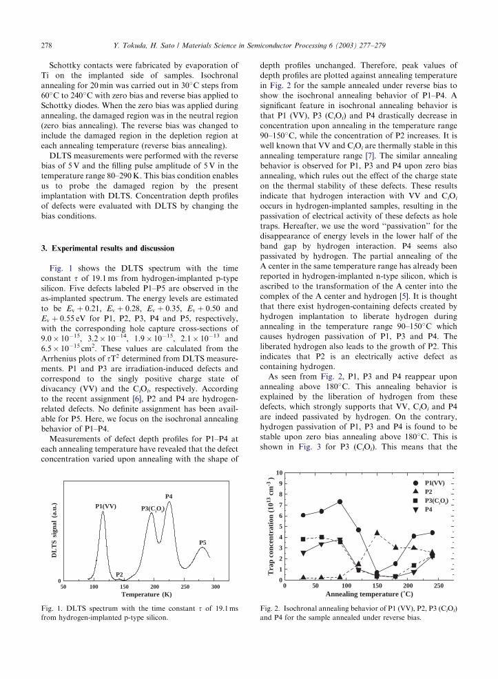
Fig. 1 shows the DLTS spectrum with the time
constant t of 19.1ms from hydrogen-implanted p-type
silicon. Five defects labeled P1–P5 are observed in the
as-implanted spectrum. The energy levels are estimated
to be Ev þ 0:21; Ev þ 0:28; Ev þ 0:35; Ev þ 0:50 and
Ev þ 0:55 eV for P1, P2, P3, P4 and P5, respectively,
with the corresponding hole capture cross-sections of
9.0� 10�15, 3.2� 10�14, 1.9� 10�15, 2.1� 10�13 and
6.5� 10�15 cm2. These values are calculated from the
Arrhenius plots of tT2 determined from DLTS measure-
ments. P1 and P3 are irradiation-induced defects and
correspond to the singly positive charge state of
divacancy (VV) and the CiOi, respectively. According
to the recent assignment [6], P2 and P4 are hydrogen-
related defects. No definite assignment has been avail-
able for P5. Here, we focus on the isochronal annealing
behavior of P1–P4.
Measurements of defect depth profiles for P1–P4 at
each annealing temperature have revealed that the defect
concentration varied upon annealing with the shape of
50 100 150 200 250 3000
P5
P4
P3(CiOi)
P2
P1(VV)
Temperature (K)
DL
TS
sign
al (
a.u.
)
Fig. 1. DLTS spectrum with the time constant t of 19.1ms
from hydrogen-implanted p-type silicon.
depth profiles unchanged. Therefore, peak values of
depth profiles are plotted against annealing temperature
in Fig. 2 for the sample annealed under reverse bias to
show the isochronal annealing behavior of P1–P4. A
significant feature in isochronal annealing behavior is
that P1 (VV), P3 (CiOi) and P4 drastically decrease in
concentration upon annealing in the temperature range
90–150�C, while the concentration of P2 increases. It is
well known that VV and CiOi are thermally stable in this
annealing temperature range [7]. The similar annealing
behavior is observed for P1, P3 and P4 upon zero bias
annealing, which rules out the effect of the charge state
on the thermal stability of these defects. These results
indicate that hydrogen interaction with VV and CiOi
occurs in hydrogen-implanted samples, resulting in the
passivation of electrical activity of these defects as hole
traps. Hereafter, we use the word ‘‘passivation’’ for the
disappearance of energy levels in the lower half of the
band gap by hydrogen interaction. P4 seems also
passivated by hydrogen. The partial annealing of the
A center in the same temperature range has already been
reported in hydrogen-implanted n-type silicon, which is
ascribed to the transformation of the A center into the
complex of the A center and hydrogen [5]. It is thought
that there exist hydrogen-containing defects created by
hydrogen implantation to liberate hydrogen during
annealing in the temperature range 90–150�C which
causes hydrogen passivation of P1, P3 and P4. The
liberated hydrogen also leads to the growth of P2. This
indicates that P2 is an electrically active defect as
containing hydrogen.
As seen from Fig. 2, P1, P3 and P4 reappear upon
annealing above 180�C. This annealing behavior is
explained by the liberation of hydrogen from these
defects, which strongly supports that VV, CiOi and P4
are indeed passivated by hydrogen. On the contrary,
hydrogen passivation of P1, P3 and P4 is found to be
stable upon zero bias annealing above 180�C. This is
shown in Fig. 3 for P3 (CiOi). This means that the
0 50 100 150 200 2500
1
2
3
4
5
6
7
8
9
10
Annealing temperature ( ̊C)
P1(VV)P2P3(CiOi)P4
Tra
p co
ncen
trat
ion
(1013
cm
-3 )
Fig. 2. Isochronal annealing behavior of P1 (VV), P2, P3 (CiOi)
and P4 for the sample annealed under reverse bias.

ARTICLE IN PRESS
0 50 100 150 200 2500
1
2
3
4
5
Tra
p co
ncen
trat
ion
(1013
cm
-3 ) P3(CiOi)
revers bias annealingzero bias annealing
Annealing temperature (˚C)
Fig. 3. Isochronal annealing behavior of P3 (CiOi) under zero
and reverse bias.
Y. Tokuda, H. Sato / Materials Science in Semiconductor Processing 6 (2003) 277–279 279
reappearance of P1, P3 and P4 upon reverse bias
annealing is due to the field drift of hydrogen dissociated
from these defects as positively charged species. It is
thought that the dissociated hydrogen from irradiation-
induced defects again associates with these defects under
no electric field.
The occurrence of hydrogen passivation of VV is
consistent with the previous reports [2–4,6]. However, as
pointed out earlier, there is some discrepancy in the
literature on the effect of hydrogen on CiOi [2,3,6].
Comparison of our isochronal annealing behavior under
zero and reverse bias supports that the CiOi pair is
indeed passivated by hydrogen. On the other hand, the
isochronal annealing behavior of P2 confirms the
previous assignment that this level is the hydrogen-
related defect [6]. It is noted from Fig. 2 that the
annealing behavior of P4 is similar to that for VV and
CiOi. This seems to suggest that P4 is the irradiation-
induced defect rather than the hydrogen-related defect,
which is inconsistent with the previous assignment by
Fatima et al. [6]. In fact, a defect corresponding to P4
has been observed in boron-implanted samples [6,8].
However, no production of this defect has been revealed
in carbon- and helium-implanted samples [6]. Further
study is necessary to identify P4.
4. Summary
Comparison of zero and reverse bias annealing in
hydrogen-implanted p-type silicon indicates that hydro-
gen interaction with CiOi pair occurs together with VV,
resulting in their passivation. These defects remain
passivated at least around 240�C under no electric field.
The hydrogen interaction with levels at Ev þ 0:50 and
Ev þ 0:28 eV suggests that these are irradiation-induced
and hydrogen-related defects, respectively.
References
[1] Pearton SJ, Coebett JW, Stavola M. Hydrogen in crystalline
semiconductors. Berlin: Springer; 1992.
[2] Qun GG, Du YC, Yao XC. Hydrogen behavior and
hydrogen-related defects in single crystal silicon. Mater Sci
For 1986;10–12:563.
[3] Feklisova OV, Yarykin NA. Transformation of deep-level
spectrum of irradiated silicon due to hydrogenation under
wet chemical etching. Semicond Sci Technol 1997;12:742.
[4] Tokuda Y. Deep-level transient spectroscopy study of
hydrogen-related traps formed by wet chemical etching in
electron-irradiated n-type silicon. Jpn J Appl Phys
1998;37:1815.
[5] Tokuda Y, Ito A. Annihilation and formation of electron
traps in hydrogen-implanted n-type silicon by light illumi-
nation. Mater Sci Eng B 2000;71:1.
[6] Fatima S, Jagadish C, Lalita J, Svensson BG, Hallen A.
J Appl Phys 1999;85:2562.
[7] Kimerling LC. Defects states in electron-bombarded silicon:
capacitance transient analyses. Inst Phys Conf Ser
1997;31:221.
[8] Tokuda Y, Iwata H. Partial annealing of defects in boron-
implanted p-type silicon by hydrogen implantation. Mater
Res Soc Symp Proc 2002;719:341.