Embed Size (px)
Citation preview

I T ’ S T I M E F O R I N T E G R A T I O N !
NTEGRA’s name is derived from many sources.
It came from classical languages for ages associated with pure science. In Latin, word ‘integer’ means perfect, absolute, or complete. The concept of
‘completeness’ refl ects the NanoLaboratory concept: each system serves as a core for the whole laboratory. Moreover, ancient roots can be seen in the name of
every model – from Solaris and Prima to Vita and Spectra.
The fi rst two letters in NTEGRA are closely connected with our company name, NT-MDT, which in turn refers to the initial letters in word
NanoTechnology.
Copyright © NT-MDT, 20104
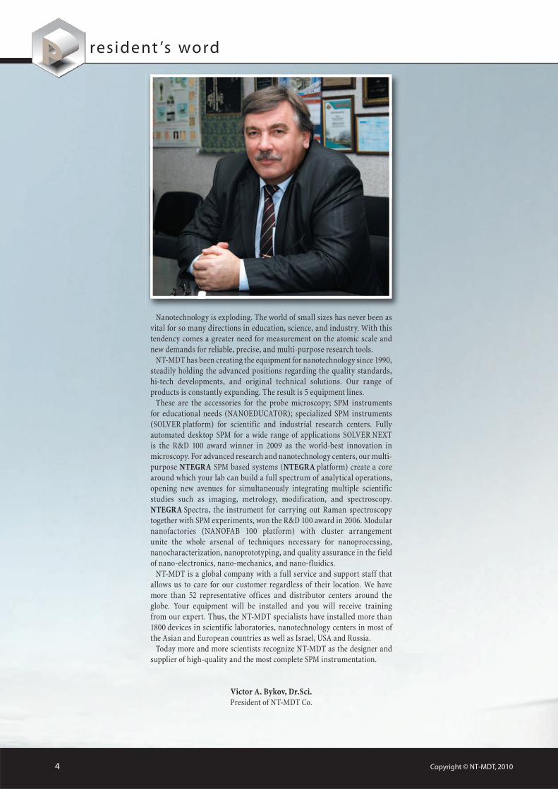
resident ’s word
Nanotechnology is exploding. The world of small sizes has never been as vital for so many directions in education, science, and industry. With this tendency comes a greater need for measurement on the atomic scale and new demands for reliable, precise, and multi-purpose research tools.
NT-MDT has been creating the equipment for nanotechnology since 1990, steadily holding the advanced positions regarding the quality standards, hi-tech developments, and original technical solutions. Our range of products is constantly expanding. The result is 5 equipment lines.
These are the accessories for the probe microscopy; SPM instruments for educational needs (NANOEDUCATOR); specialized SPM instruments (SOLVER platform) for scientific and industrial research centers. Fully automated desktop SPM for a wide range of applications SOLVER NEXT is the R&D 100 award winner in 2009 as the world-best innovation in microscopy. For advanced research and nanotechnology centers, our multi-purpose NTEGRA SPM based systems (NTEGRA platform) create a core around which your lab can build a full spectrum of analytical operations, opening new avenues for simultaneously integrating multiple scientific studies such as imaging, metrology, modification, and spectroscopy. NTEGRA Spectra, the instrument for carrying out Raman spectroscopy together with SPM experiments, won the R&D 100 award in 2006. Modular nanofactories (NANOFAB 100 platform) with cluster arrangement unite the whole arsenal of techniques necessary for nanoprocessing, nanocharacterization, nanoprototyping, and quality assurance in the field of nano-electronics, nano-mechanics, and nano-fluidics.
NT-MDT is a global company with a full service and support staff that allows us to care for our customer regardless of their location. We have more than 52 representative offices and distributor centers around the globe. Your equipment will be installed and you will receive training from our expert. Thus, the NT-MDT specialists have installed more than 1800 devices in scientific laboratories, nanotechnology centers in most of the Asian and European countries as well as Israel, USA and Russia.
Today more and more scientists recognize NT-MDT as the designer and supplier of high-quality and the most complete SPM instrumentation.
Victor A. Bykov, Dr.Sci.President of NT-MDT Co.
Copyright © NT-MDT, 2010 5
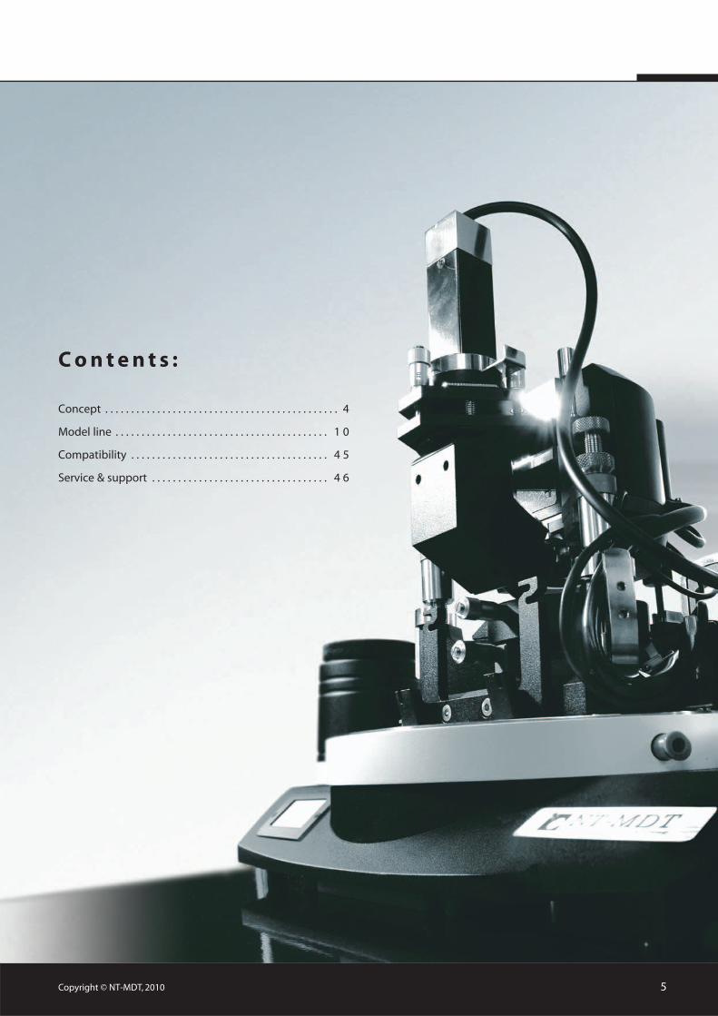
C o n t e n t s :
Concept . . . . . . . . . . . . . . . . . . . . . . . . . . . . . . . . . . . . . . . . . . . . . 4
Model line . . . . . . . . . . . . . . . . . . . . . . . . . . . . . . . . . . . . . . . . . 1 0
Compatibility . . . . . . . . . . . . . . . . . . . . . . . . . . . . . . . . . . . . . . 4 5
Service & support . . . . . . . . . . . . . . . . . . . . . . . . . . . . . . . . . . 4 6
Copyright © NT-MDT, 20106
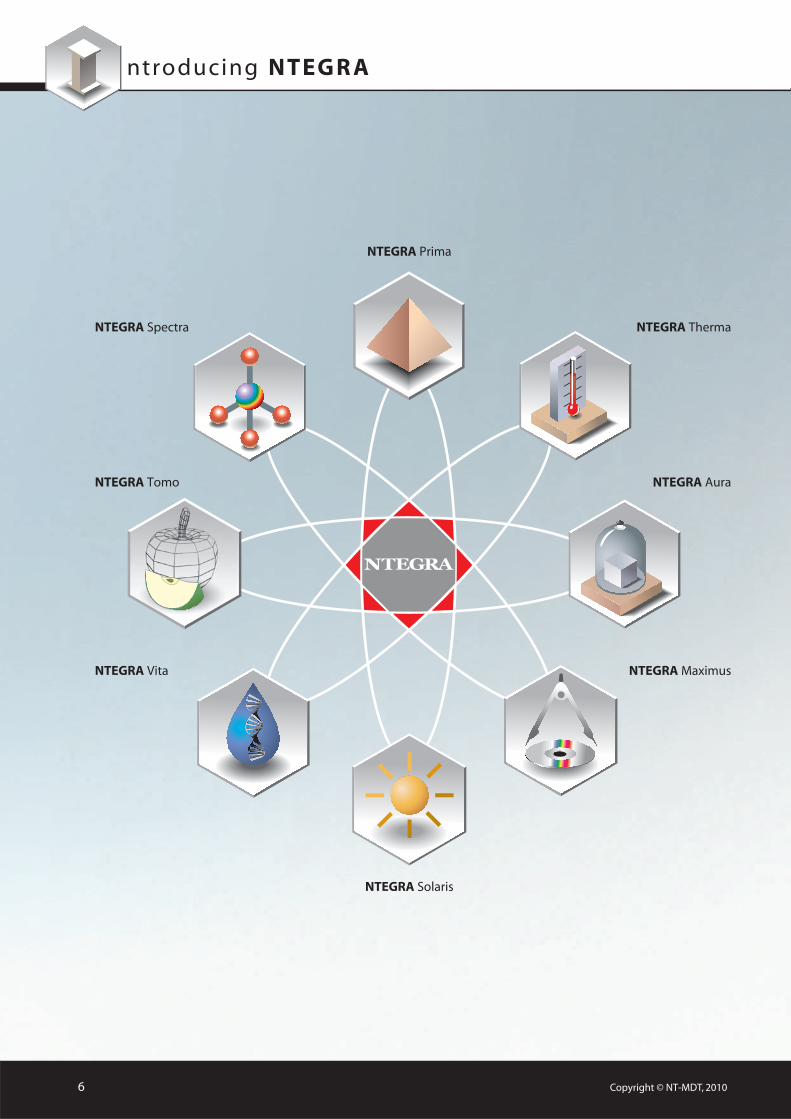
ntroducing NTEG R A
NTEGRA Spectra
NTEGRA Tomo
NTEGRA Vita
NTEGRA Therma
NTEGRA Aura
NTEGRA Maximus
NTEGRA Prima
NTEGRA Solaris
Copyright © NT-MDT, 2010 7
One integrated concept, many built-for-purpose modelsCurrently NT-MDT offers eight versions of the systems assembled on the NTEGRA platform. For
superior performance, each system has its own application specialization.
NTEGRA Prima is a high-resolution, low-noise SPM ideal for the multi-user labs. Integrated optics coupled to the SPM provides imaging of samples with almost continuous zoom from the millimeter to angstrom range.
NTEGRA Therma is an effective solution for SPM measurements either at constant temperatures from -30 °C to 300 °C or with changing temperature. Our low-drift THead™ maintains a drift of less than 10 nm/°C.
NTEGRA Aura is a high-sensitive system perfectly suited for measurements in vacuum up to 10-3 torr or under controlled atmosphere environments.
NTEGRA Maximus performs high throughput screening of multiple samples as well as measurements on large samples.
NTEGRA Solaris uses Scanning Near-Field Optical Microscopy (SNOM) to investigate optical properties beyond the diffraction limit.
NTEGRA Vita combines the strengths of the excellent SPM with perfect optical microscope for biological and medical applications.
NTEGRA Tomo, industry-leading NT-MDT invention, integrates the SPM with an ultramicrotome to perform AFM tomography and 3D reconstruction of biological and materials ultrastructure never seen before.
NTEGRA Spectra, the R&D 100 award winner in 2006, integrates the SPM with Raman spectroscopy and laser confocal microscopy to study the distribution of chemical properties with molecular resolution.
NTEGRA conceptNTEGRA is a revolutionary technological concept. It was designed specifically to form an
SPM based platform within which cutting-edge methods from other scientific analyses such as spectroscopy and sample preparation could be integrated. All the systems assembled on NTEGRA platform share the same SPM core, electronic controllers, and software. As a result, any NTEGRA base unit built for one particular application can easily be modified into a system suitable for another, very different application. The result: a complete solution for research and industry which provides a scientist with groundbreaking results.
Central to NT-MDT’s philosophy of the integrated lab is NTEGRA line
Copyright © NT-MDT, 20108
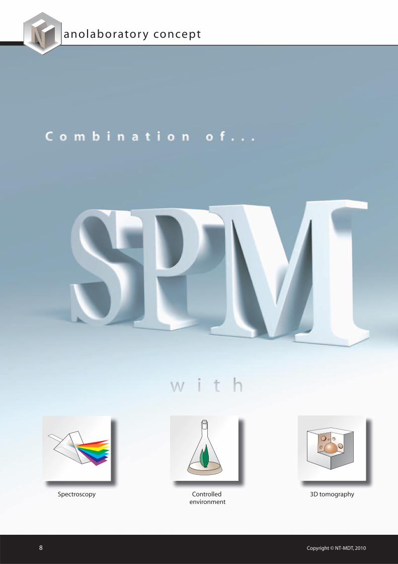
anolaborator y concept
3D tomographySpectroscopy Controlled environment
Copyright © NT-MDT, 2010 9
SPM was a method strictly oriented to a narrow sector of material sciences for many years. Times have changed. Today it is a part of the mainstream. There is hardly a branch of science from biology to chemistry, from physics to nanotechnology, where the SPM is not used. This wide-spread applicability dictates a new need for integration. The SPM has been called on to merge with the sophisticated infrastructure of the modern scientific laboratory.
Almost any of today’s serious commercial SPM can be adapted to work in vacuum or in controlled gaseous or liquid environment, but to date, none have achieved real integration of multiple methods, including non-SPM techniques, within a global and convenient interface. NT-MDT has answered the call, launching the new NTEGRA Probe NanoLaboratory. NTEGRA allows the sample of interest to be studied by powerful and up-to-the-minute non-SPM methods without compromising SPM quality. It uniquely integrates SPM with optical observation, chemical composition mapping, and even nano-tomography, opening a new universe of correlative analyses applicable to all areas of modern science. Furthermore, its open architecture in hardware, software, and signal integration provides a portal for you to customize and expand this list to fit your applications.
Optical methods High throughput screening
Other non-SPM methods
Copyright © NT-MDT, 201010
Ultratome module SPM
platform
Smart solution for instrument re-specialization
NTEGRATomo
NTEGRAMaximus
NTEGRAAura
NTEGRATherma
NTEGRAPrima
pecial iz ation
Extreme stability for long-term measurements;
wide temperature range
Large samples and/or high throughput
screening
Low vacuum and enhanced non-contact
AFM sensitivity
AFM of soft materials in 3D
Multifunctional SPM
Copyright © NT-MDT, 2010 11
Optics conjunction
module
NTEGRASolaris
NTEGRASpectra
NTEGRAVita
What do you do when your lab is involved in multiple distinct projects requiring SPM-based instruments with radically different focus? Should you invest in multiple devices? Should you spend the time learning multiple pieces of software? Relinquish space for multiple instruments? Contact multiple service teams for support and tuning? And what happens when still another researchers joins you? Add still further complexity?
NTEGRA offers an elegant solution. Universal platform design, universal electronics, universal software — all you need to convert one NTEGRA model into another is to add the necessary accessory. No matter what the configuration, NTEGRA will retain its excellent quality and performance. Find your area of interest on the pages below and contact us to set up the most versatile system for you.
NTEGRA Probe Nanolaboratory: SPM that grows as your lab grows.
Spectral analysis of the matter down to molecular resolution (SERS, TERS)
Living objects and molecules in native environment
Optical properties beyond the diffraction limits
odel l ine
12 Copyright © NT-MDT, 2010
NTEGRA Prima . . . . . . . . . . . . . . . . . . . . . . . . . . . . . . . . . . . . . . . . . . . . . . 11
NTEGRA Therma . . . . . . . . . . . . . . . . . . . . . . . . . . . . . . . . . . . . . . . . . . . 15
NTEGRA Aura . . . . . . . . . . . . . . . . . . . . . . . . . . . . . . . . . . . . . . . . . . . . . . . 19
NTEGRA Maximus . . . . . . . . . . . . . . . . . . . . . . . . . . . . . . . . . . . . . . . . . . 23
NTEGRA Solaris . . . . . . . . . . . . . . . . . . . . . . . . . . . . . . . . . . . . . . . . . . . . . 27
NTEGRA Vita . . . . . . . . . . . . . . . . . . . . . . . . . . . . . . . . . . . . . . . . . . . . . . . . 31
NTEGRA Tomo . . . . . . . . . . . . . . . . . . . . . . . . . . . . . . . . . . . . . . . . . . . . . . 35
NTEGRA Spectra . . . . . . . . . . . . . . . . . . . . . . . . . . . . . . . . . . . . . . . . . . . . 39

Benefit from precise motion
NTEGRA Prima
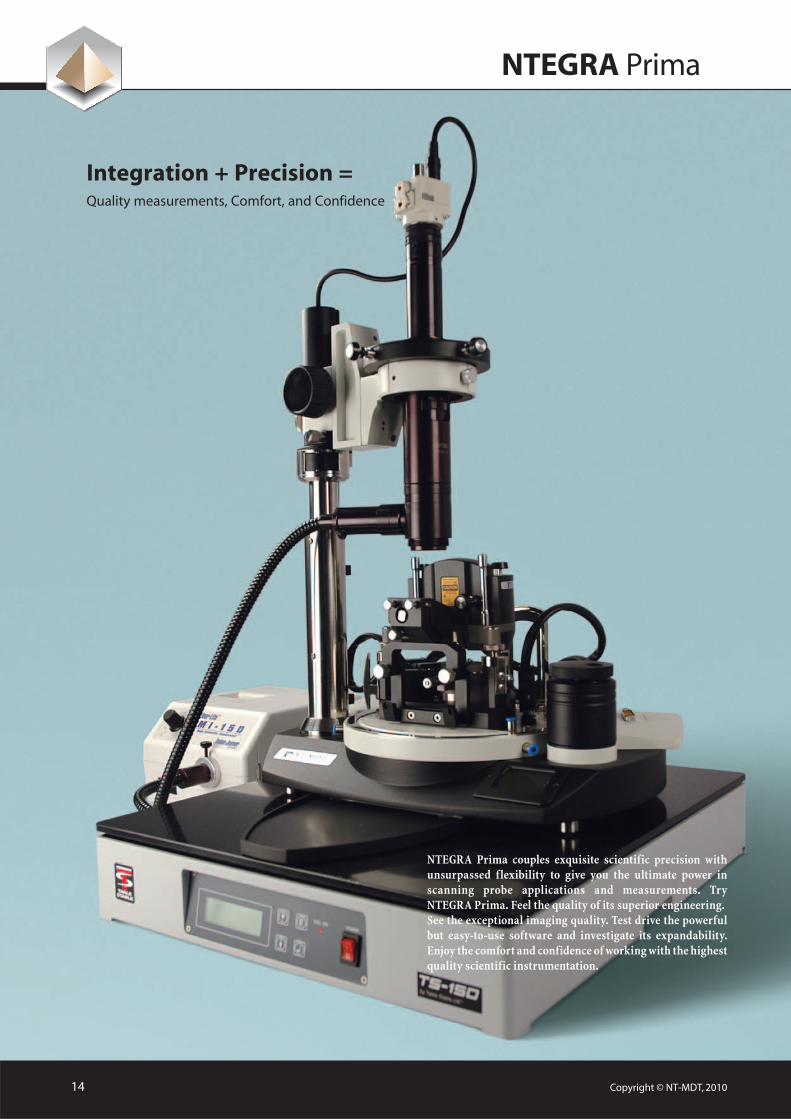
NTEGRA Prima
NTEGRA Prima couples exquisite scientific precision with unsurpassed flexibility to give you the ultimate power in scanning probe applications and measurements. Try NTEGRA Prima. Feel the quality of its superior engineering.See the exceptional imaging quality. Test drive the powerful but easy-to-use software and investigate its expandability. Enjoy the comfort and confidence of working with the highest quality scientific instrumentation.
Copyright © NT-MDT, 201014
Integration + Precision =Quality measurements, Comfort, and Confidence
NTEGRA Prima
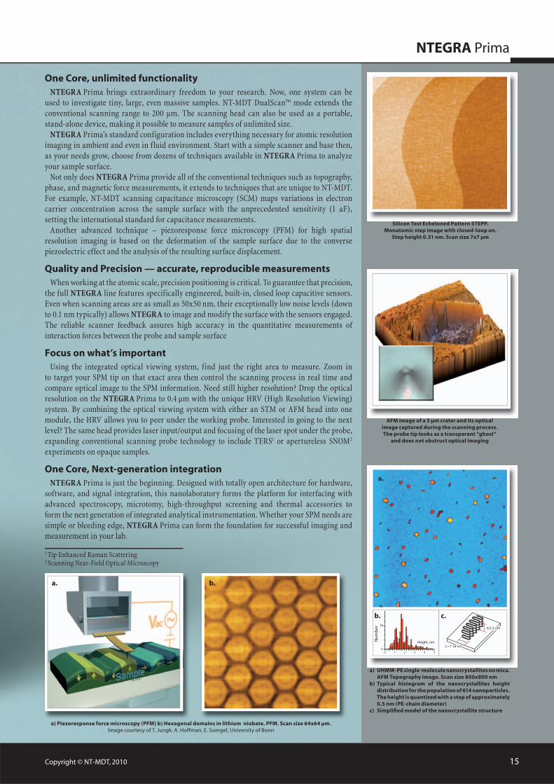
Silicon Test Echeloned Pattern STEPP. Monatomic step image with closed-loop on.
Step height 0.31 nm. Scan size 7x7 µm
a) Piezoresponse force microscopy (PFM) b) Hexagonal domains in lithium niobate. PFM. Scan size 64x64 µm.Image courtesy of T. Jungk, A. Hoffman, E. Soergel, University of Bonn
AFM image of a 5 µm crater and its optical image captured during the scanning process. The probe tip looks as a transparent “ghost”
and does not obstruct optical imaging
a) UHMW-PE single-molecule nanocrystallites on mica. AFM Topography image. Scan size 800x800 nmb) Typical histogram of the nanocrystallites height distribution for the population of 614 nanoparticles. The height is quantized with a step of approximately 0.5 nm (PE-chain diameter)c) Simplifi ed model of the nanocrystallite structure
a.
b. c.
Nu
mb
er
Height, nm
a. b.
Copyright © NT-MDT, 2010 15
One Core, unlimited functionalityNTEGRA Prima brings extraordinary freedom to your research. Now, one system can be
used to investigate tiny, large, even massive samples. NT-MDT DualScan™ mode extends the conventional scanning range to 200 µm. The scanning head can also be used as a portable, stand-alone device, making it possible to measure samples of unlimited size.
NTEGRA Prima’s standard configuration includes everything necessary for atomic resolution imaging in ambient and even in f luid environment. Start with a simple scanner and base then, as your needs grow, choose from dozens of techniques available in NTEGRA Prima to analyze your sample surface.
Not only does NTEGRA Prima provide all of the conventional techniques such as topography, phase, and magnetic force measurements, it extends to techniques that are unique to NT-MDT. For example, NT-MDT scanning capacitance microscopy (SCM) maps variations in electron carrier concentration across the sample surface with the unprecedented sensitivity (1 aF), setting the international standard for capacitance measurements.
Another advanced technique – piezoresponse force microscopy (PFM) for high spatial resolution imaging is based on the deformation of the sample surface due to the converse piezoelectric effect and the analysis of the resulting surface displacement.
Quality and Precision — accurate, reproducible measurementsWhen working at the atomic scale, precision positioning is critical. To guarantee that precision,
the full NTEGRA line features specifically engineered, built-in, closed loop capacitive sensors. Even when scanning areas are as small as 50x50 nm, their exceptionally low noise levels (down to 0.1 nm typically) allows NTEGRA to image and modify the surface with the sensors engaged.The reliable scanner feedback assures high accuracy in the quantitative measurements of interaction forces between the probe and sample surface
Focus on what’s importantUsing the integrated optical viewing system, find just the right area to measure. Zoom in
to target your SPM tip on that exact area then control the scanning process in real time and compare optical image to the SPM information. Need still higher resolution? Drop the optical resolution on the NTEGRA Prima to 0.4 µm with the unique HRV (High Resolution Viewing) system. By combining the optical viewing system with either an STM or AFM head into one module, the HRV allows you to peer under the working probe. Interested in going to the next level? The same head provides laser input/output and focusing of the laser spot under the probe, expanding conventional scanning probe technology to include TERS1 or apertureless SNOM2 experiments on opaque samples.
One Core, Next-generation integrationNTEGRA Prima is just the beginning. Designed with totally open architecture for hardware,
software, and signal integration, this nanolaboratory forms the platform for interfacing with advanced spectroscopy, microtomy, high-throughput screening and thermal accessories to form the next generation of integrated analytical instrumentation. Whether your SPM needs are simple or bleeding edge, NTEGRA Prima can form the foundation for successful imaging and measurement in your lab.
1 Tip Enhanced Raman Scattering2 Scanning Near-Field Optical Microscopy
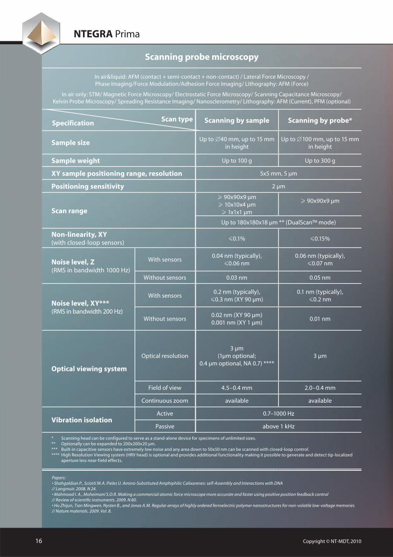
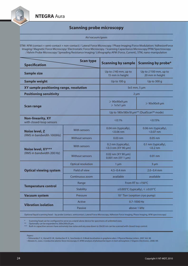
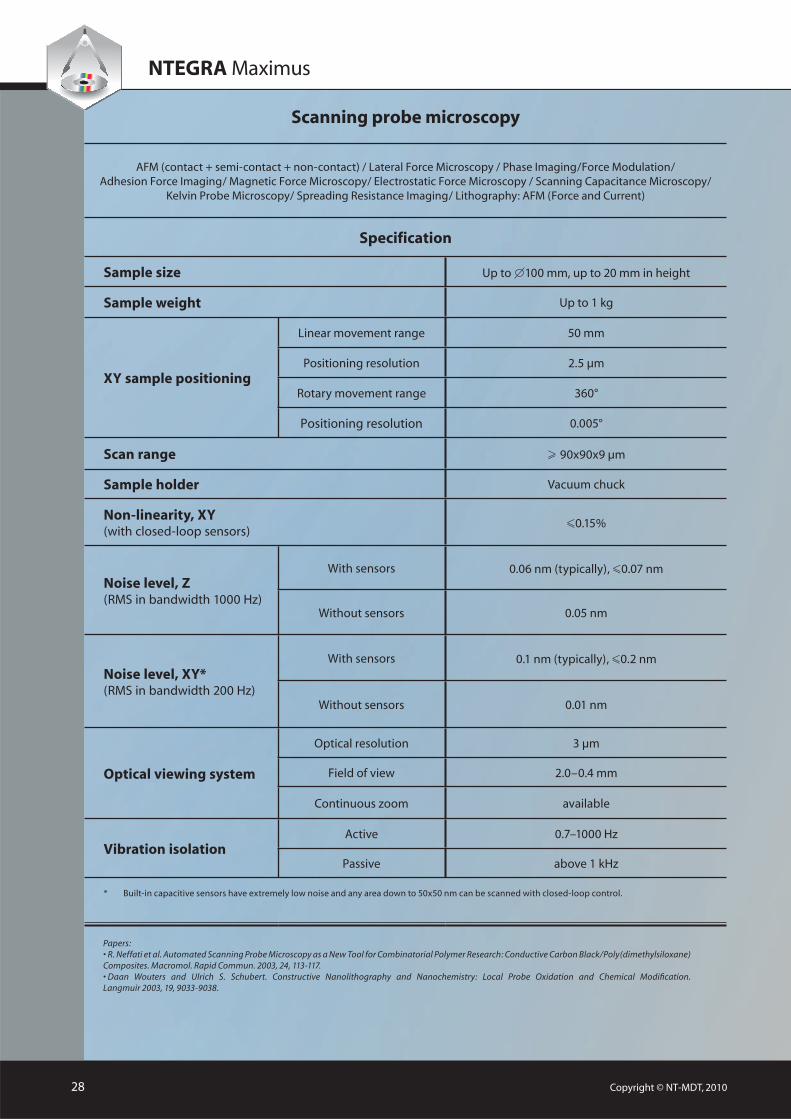
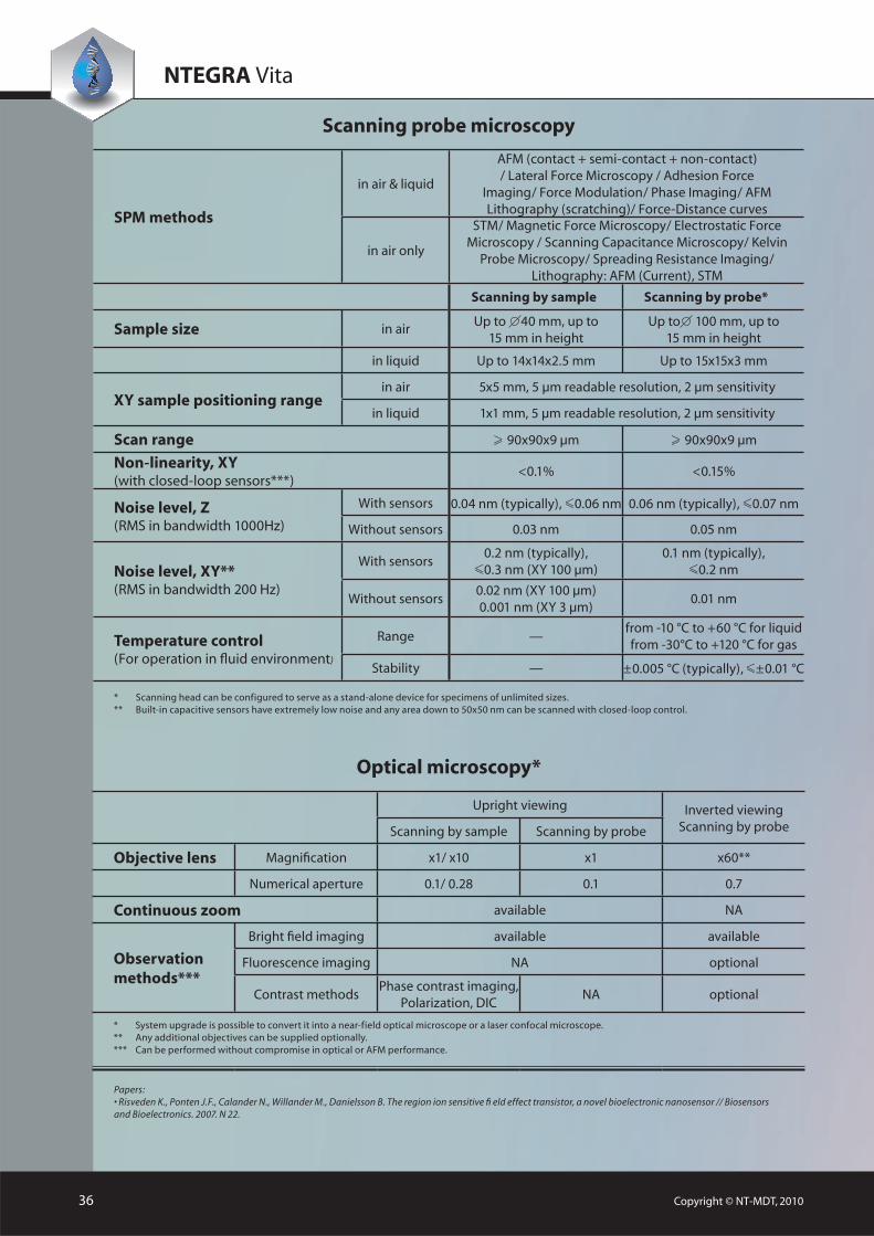
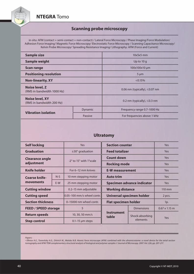
Scanning probe microscopy
In air&liquid: AFM (contact + semi-contact + non-contact) / Lateral Force Microscopy / Phase Imaging/Force Modulation/Adhesion Force Imaging/ Lithography: AFM (Force)
In air only: STM/ Magnetic Force Microscopy/ Electrostatic Force Microscopy/ Scanning Capacitance Microscopy/ Kelvin Probe Microscopy/ Spreading Resistance Imaging/ Nanosclerometry/ Lithography: AFM (Current), PFM (optional)
Specification Scan type Scanning by sample Scanning by probe*
Sample size Up to 40 mm, up to 15 mm in height
Up to 100 mm, up to 15 mm in height
Sample weight Up to 100 g Up to 300 g
XY sample positioning range, resolution 5x5 mm, 5 µm
Positioning sensitivity 2 µm
Scan range
� 90x90x9 µm� 10x10x4 µm� 1x1x1 µm
� 90x90x9 µm
Up to 180x180x18 µm ** (DualScan™ mode)
Non-linearity, XY(with closed-loop sensors)
�0.1% �0.15%
Noise level, Z (RMS in bandwidth 1000 Hz)
With sensors 0.04 nm (typically),
�0.06 nm0.06 nm (typically),
�0.07 nm
Without sensors 0.03 nm 0.05 nm
Noise level, XY***(RMS in bandwidth 200 Hz)
With sensors0.2 nm (typically),
�0.3 nm (XY 90 µm)0.1 nm (typically),
�0.2 nm
Without sensors0.02 nm (XY 90 µm)0.001 nm (XY 1 µm)
0.01 nm
Optical viewing system
Optical resolution 3 µm
(1µm optional; 0.4 µm optional, NA 0.7) ****
3 µm
Field of view 4.5–0.4 mm 2.0–0.4 mm
Continuous zoom available available
Vibration isolationActive 0.7–1000 Hz
Passive above 1 kHz
* Scanning head can be configured to serve as a stand-alone device for specimens of unlimited sizes.** Optionally can be expanded to 200x200x20 µm.*** Built-in capacitive sensors have extremely low noise and any area down to 50x50 nm can be scanned with closed-loop control.**** High Resolution Viewing system (HRV head) is optional and provides additional functionality making it possible to generate and detect tip-localized aperture less near-field effects.
Papers:• Shahgaldian P., Sciotti M.A. Pieles U. Amino-Substituted Amphiphilic Calixarenes: self-Assembly and Interactions with DNA// Langmuir. 2008. N 24.• Mahmood I. A., Moheimani S.O.R. Making a commercial atomic force microscope more accurate and faster using positive position feedback control // Review of scientifi c instruments. 2009. N 80.• Hu Zhijun, Tian Mingwen, Nysten B., and Jonas A.M. Regular arrays of highly ordered ferroelectric polymer nanostructures for non-volatile low-voltage memories// Nature materials. 2009. Vol. 8.
Copyright © NT-MDT, 201016
NTEGRA Prima

Heating and cooling
NTEGRA Therma
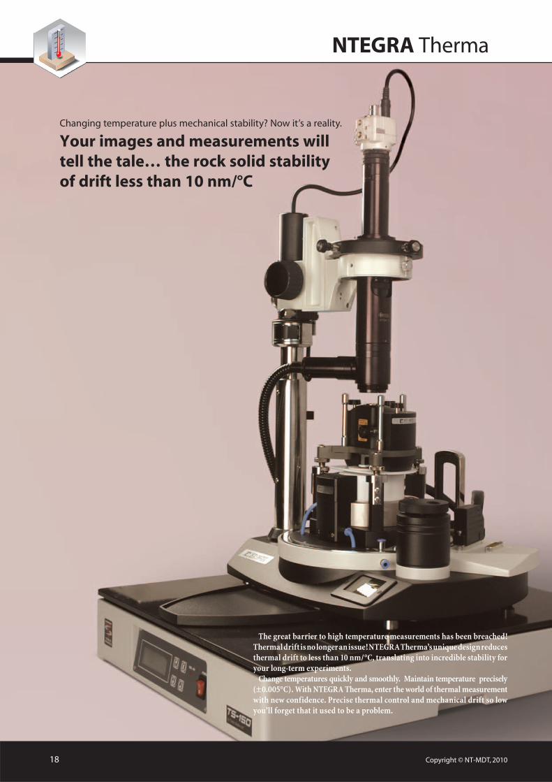
NTEGRA Therma
The great barrier to high temperature measurements has been breached! Thermal drift is no longer an issue! NTEGRA Therma’s unique design reduces thermal drift to less than 10 nm/°C, translating into incredible stability foryour long-term experiments.
Change temperatures quickly and smoothly. Maintain temperature precisely (±0.005°C). With NTEGRA Therma, enter the world of thermal measurement with new confidence. Precise thermal control and mechanical drift so low you’ll forget that it used to be a problem.
Copyright © NT-MDT, 201018
Changing temperature plus mechanical stability? Now it’s a reality.
Your images and measurements will tell the tale… the rock solid stability of drift less than 10 nm/°C
NTEGRA Therma
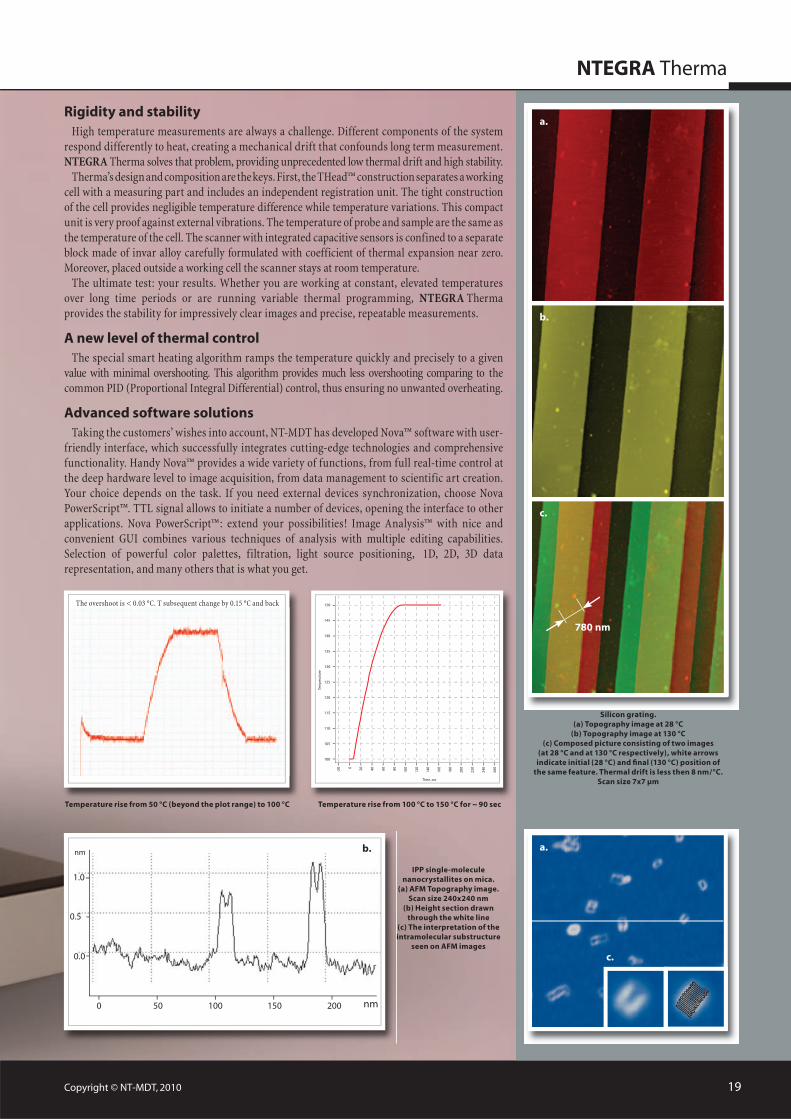
Silicon grating. (a) Topography image at 28 °C
(b) Topography image at 130 °C(c) Composed picture consisting of two images
(at 28 °C and at 130 °C respectively), white arrows indicate initial (28 °C) and fi nal (130 °C) position of
the same feature. Thermal drift is less then 8 nm/°C.Scan size 7x7 µm
Temperature rise from 100 °C to 150 °C for ~ 90 sec
a.
b.
c.
nm
nm
0.5
0.0
0 50 100 150 200
IPP single-molecule nanocrystallites on mica.
(a) AFM Topography image.Scan size 240x240 nm
(b) Height section drawn through the white line
(c) The interpretation of the intramolecular substructure
seen on AFM images
a.
c.
Temperature rise from 50 °C (beyond the plot range) to 100 °C
780 nm
1.0
The overshoot is < 0.03 °C. T subsequent change by 0.15 °C and back
b.
19Copyright © NT-MDT, 2010
Rigidity and stabilityHigh temperature measurements are always a challenge. Different components of the system
respond differently to heat, creating a mechanical drift that confounds long term measurement. NTEGRA Therma solves that problem, providing unprecedented low thermal drift and high stability.
Therma’s design and composition are the keys. First, the THead™ construction separates a working cell with a measuring part and includes an independent registration unit. The tight construction of the cell provides negligible temperature difference while temperature variations. This compact unit is very proof against external vibrations. The temperature of probe and sample are the same as the temperature of the cell. The scanner with integrated capacitive sensors is confined to a separate block made of invar alloy carefully formulated with coefficient of thermal expansion near zero. Moreover, placed outside a working cell the scanner stays at room temperature.
The ultimate test: your results. Whether you are working at constant, elevated temperatures over long time periods or are running variable thermal programming, NTEGRA Therma provides the stability for impressively clear images and precise, repeatable measurements.
A new level of thermal controlThe special smart heating algorithm ramps the temperature quickly and precisely to a given
value with minimal overshooting. This algorithm provides much less overshooting comparing to the common PID (Proportional Integral Differential) control, thus ensuring no unwanted overheating.
Advanced software solutionsTaking the customers’ wishes into account, NT-MDT has developed Nova™ software with user-
friendly interface, which successfully integrates cutting-edge technologies and comprehensive functionality. Handy Nova™ provides a wide variety of functions, from full real-time control at the deep hardware level to image acquisition, from data management to scientific art creation. Your choice depends on the task. If you need external devices synchronization, choose Nova PowerScript™. TTL signal allows to initiate a number of devices, opening the interface to other applications. Nova PowerScript™: extend your possibilities! Image Analysis™ with nice and convenient GUI combines various techniques of analysis with multiple editing capabilities. Selection of powerful color palettes, filtration, light source positioning, 1D, 2D, 3D data representation, and many others that is what you get.

Papers:• Wang W., Ciselli P., Kuznetsov E., Peijs T., Barber A.H. Effective reinforcement in carbon nanotube-polymer composites. Philos.Transact.A Math.Phys.Eng.Sci.2008; 18192168 (published online)
Scanning probe microscopy
STM/ AFM (contact + semi-contact + non-contact) / Lateral Force Microscopy / Phase Imaging/Force Modulation/ Adhesion Force Imaging/ Magnetic Force Microscopy/ Electrostatic Force Microscopy/ Lithography: AFM (Force)
Specification Scan type Scanning by sample
Sample sizeAmbient environment
Up to 40 mm, up to 15 mm in height
Heating or cooling10x10x1.5 mm15x12x1.5 mm
XY sample positioning range, resolution 5x5 mm, 5 µm
Positioning sensitivity 2 µm
Temperature controlRange From -30°C to +80°C/ from RT to +300 °C
Stability±0.005 (typically),
better than ±0.01°C
Scan range
-30 °C � +80 °C/ RT � +200 °C � 10x10x6 µm
Ambient conditions/RT � +150 °C
� 90x90x9 µm� 1x1x1 µm
RT � +300 °C � 90x90x9 µm
Thermal drift*(typically)
XY 15 nm/°C
Z 10 nm/°C
Non-linearity, XYwith closed-loop sensors
<0.2%
Noise level, Z (RMS in bandwidth 1000Hz)
With sensors 0.04 nm (typically),
�0.06 nm
Without sensors 0.03 nm
Noise level, XY**(RMS in bandwidth 200 Hz)
With sensors
0.2 nm (typically), �0.3 nm (XY 90 µm)0.025 nm (typically), �0.04 nm (XY 10 µm)
Without sensors0.02 nm (XY 90 µm)
0.002 nm (XY 10 µm)0.001 nm (XY 1 µm)
Linear dimension estimation error (with sensors) ±0.5%
Optical viewing system
Optical resolution 1 µm/ 3 µm
Field of view 4.5–0.4 mm
Continuous zoom available
Vibration isolationActive 0.7–1000 Hz
Passive above 1 kHz
* For temperature range –30 °C � +80 °C and RT � +200.** Built-in capacitive sensors have extremely low noise and any area down to 50x50 nm can be scanned with closed-loop control.
NTEGRA Therma
Copyright © NT-MDT, 201020
Pure environment
NTEGRA Aura
NTEGRA Aura
Copyright © NT-MDT, 201022
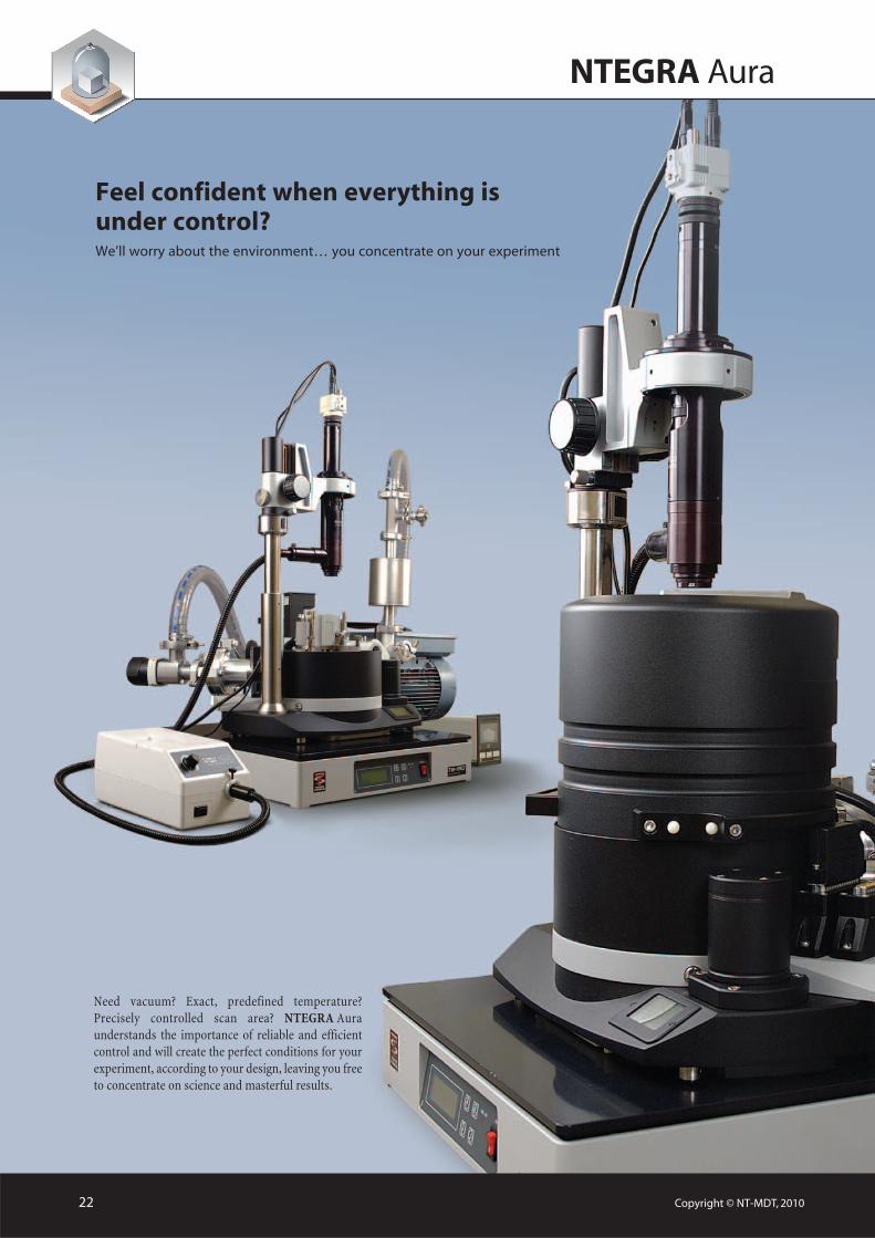
Need vacuum? Exact, predefined temperature? Precisely controlled scan area? NTEGRA Aura understands the importance of reliable and efficient control and will create the perfect conditions for your experiment, according to your design, leaving you free to concentrate on science and masterful results.
Feel confident when everything isunder control?We’ll worry about the environment… you concentrate on your experiment
NTEGRA Aura
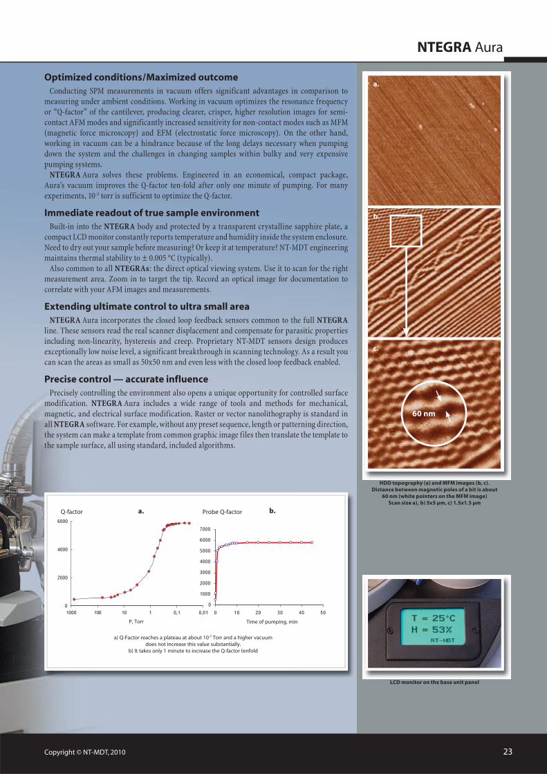
HDD topography (a) and MFM images (b, c). Distance between magnetic poles of a bit is about
60 nm (white pointers on the MFM image)Scan size a), b) 5x5 µm, c) 1.5x1.5 µm
60 nm
LCD monitor on the base unit panel
a.
b.
c.
Q-factor Probe Q-factora. b.
P, Torr Time of pumping, min
a) Q-Factor reaches a plateau at about 10-1 Torr and a higher vacuum does not increase this value substantially.
b) It takes only 1 minute to increase the Q-factor tenfold
Copyright © NT-MDT, 2010 23
Optimized conditions/Maximized outcomeConducting SPM measurements in vacuum offers significant advantages in comparison to
measuring under ambient conditions. Working in vacuum optimizes the resonance frequency or “Q-factor” of the cantilever, producing clearer, crisper, higher resolution images for semi-contact AFM modes and significantly increased sensitivity for non-contact modes such as MFM (magnetic force microscopy) and EFM (electrostatic force microscopy). On the other hand, working in vacuum can be a hindrance because of the long delays necessary when pumping down the system and the challenges in changing samples within bulky and very expensive pumping systems.
NTEGRA Aura solves these problems. Engineered in an economical, compact package, Aura’s vacuum improves the Q-factor ten-fold after only one minute of pumping. For many experiments, 10-3 torr is sufficient to optimize the Q-factor.
Immediate readout of true sample environmentBuilt-in into the NTEGRA body and protected by a transparent crystalline sapphire plate, a
compact LCD monitor constantly reports temperature and humidity inside the system enclosure. Need to dry out your sample before measuring? Or keep it at temperature? NT-MDT engineering maintains thermal stability to ± 0.005 °C (typically).
Also common to all NTEGRAs: the direct optical viewing system. Use it to scan for the right measurement area. Zoom in to target the tip. Record an optical image for documentation to correlate with your AFM images and measurements.
Extending ultimate control to ultra small area NTEGRA Aura incorporates the closed loop feedback sensors common to the full NTEGRA
line. These sensors read the real scanner displacement and compensate for parasitic properties including non-linearity, hysteresis and creep. Proprietary NT-MDT sensors design produces exceptionally low noise level, a significant breakthrough in scanning technology. As a result you can scan the areas as small as 50x50 nm and even less with the closed loop feedback enabled.
Precise control — accurate influencePrecisely controlling the environment also opens a unique opportunity for controlled surface
modification. NTEGRA Aura includes a wide range of tools and methods for mechanical, magnetic, and electrical surface modification. Raster or vector nanolithography is standard in all NTEGRA software. For example, without any preset sequence, length or patterning direction, the system can make a template from common graphic image files then translate the template to the sample surface, all using standard, included algorithms.
Scanning probe microscopy
Air/vacuum/gases
STM/ AFM (contact + semi-contact + non-contact) / Lateral Force Microscopy / Phase Imaging/Force Modulation/ AdhesionForce Imaging/ Magnetic Force Microscopy/ Electrostatic Force Microscopy / Scanning Capacitance Microscopy/PFM/Spectroscopy
/ Kelvin Probe Microscopy/ Spreading Resistance Imaging/ Lithography:AFM (Force, Current), STM, nano-manipulation
Specifi cation Scan type
Scanning by sample Scanning by probe*
Sample size Up to 40 mm, up to15 mm in height
Up to 100 mm, up to 20 mm in height
Sample weight Up to 100 g Up to 300 g
XY sample positioning range, resolution 5x5 mm, 5 µm
Positioning sensitivity 2 µm
Scan range� 90x90x9 µm
� 1x1x1 µm� 90x90x9 µm
Up to 180x180x18 µm** (DualScan™ mode)
Non-linearity, XYwith closed-loop sensors
�0.1% �0.15%
Noise level, Z (RMS in bandwidth 1000Hz)
With sensors 0.04 nm (typically),
�0.06 nm0.06 nm (typically),
�0.07 nm
Without sensors 0.03 nm 0.05 nm
Noise level, XY***(RMS in bandwidth 200 Hz)
With sensors0.2 nm (typically),
�0.3 nm (XY 90 µm)0.1 nm (typically),
�0.2 nm
Without sensors0.02 nm (XY 90 µm)0.001 nm (XY 1 µm)
0.01 nm
Optical viewing system
Optical resolution 1 µm 3 µm
Field of view 4.5–0.4 mm 2.0–0.4 mm
Continuous zoom available available
Temperature controlRange From RT to +150°C
Stability ±0.005°C (typically), � ±0.01°C
Vacuum system Pressure 10-3 Torr (sorption cryo pump)
Vibration isolationActive 0.7–1000 Hz
Passive above 1 kHz
Optional liquid scanning head – by probe (contact, semicontact, Lateral Force Microscopy, Adhesion Force Imaging, Phase Imaging, AFM spectroscopy)
* Scanning head can be configured to serve as a stand-alone device for specimens of unlimited sizes.** Optionally can be expanded to 200x200x20 µm.*** Built-in capacitive sensors have extremely low noise and any area down to 50x50 nm can be scanned with closed-loop control.
NTEGRA Aura
Papers:• Tikhonenko F. V., Horsell D. W., Gorbachev R. V., Savchenko A. K.Weak localisation in graphene akes // Physical Review Letters. 2007. Vol. 98.• Alexeev A., Loos J. Conductive atomic force microscopy (C-AFM) analysis of photoactive layers in inert atmosphere // Organic Electronics. 2008. N9.
Copyright © NT-MDT, 201024
NTEGRA Maximus
Large samples and automation
NTEGRA Maximus
Copyright © NT-MDT, 201026
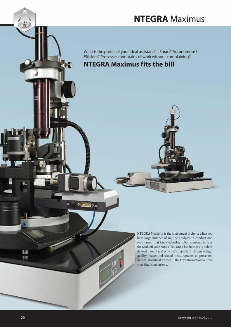
NTEGRA Maximus is the instrument of choice when you have large number of routine analyses to conduct and really need that knowledgeable robot assistant to take the work off your hands. You won’t feel how easily it does its work. You’ll just get what’s important: dozens of high quality images and related measurements, all presented in neat, statistical format… the key information to draw your final conclusions.
What is the profi le of your ideal assistant? – Smart? Autonomous? Effi cient? Processes mountains of work without complaining?
NTEGRA Maximus fits the bill
NTEGRA Maximus
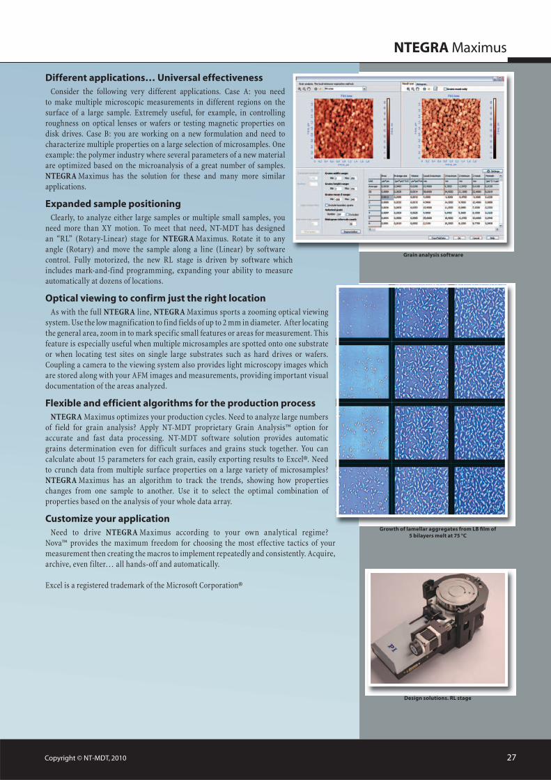
Grain analysis software
Growth of lamellar aggregates from LB fi lm of 5 bilayers melt at 75 °C
Design solutions. RL stage
Copyright © NT-MDT, 2010 27
Different applications… Universal effectiveness Consider the following very different applications. Case A: you need
to make multiple microscopic measurements in different regions on the surface of a large sample. Extremely useful, for example, in controlling roughness on optical lenses or wafers or testing magnetic properties on disk drives. Case B: you are working on a new formulation and need to characterize multiple properties on a large selection of microsamples. One example: the polymer industry where several parameters of a new material are optimized based on the microanalysis of a great number of samples. NTEGRA Maximus has the solution for these and many more similar applications.
Expanded sample positioning Clearly, to analyze either large samples or multiple small samples, you
need more than XY motion. To meet that need, NT-MDT has designed an “RL” (Rotary-Linear) stage for NTEGRA Maximus. Rotate it to any angle (Rotary) and move the sample along a line (Linear) by software control. Fully motorized, the new RL stage is driven by software which includes mark-and-find programming, expanding your ability to measure automatically at dozens of locations.
Optical viewing to confirm just the right locationAs with the full NTEGRA line, NTEGRA Maximus sports a zooming optical viewing
system. Use the low magnification to find fields of up to 2 mm in diameter. After locating the general area, zoom in to mark specific small features or areas for measurement. This feature is especially useful when multiple microsamples are spotted onto one substrate or when locating test sites on single large substrates such as hard drives or wafers. Coupling a camera to the viewing system also provides light microscopy images which are stored along with your AFM images and measurements, providing important visual documentation of the areas analyzed.
Flexible and efficient algorithms for the production processNTEGRA Maximus optimizes your production cycles. Need to analyze large numbers
of field for grain analysis? Apply NT-MDT proprietary Grain Analysis™ option for accurate and fast data processing. NT-MDT software solution provides automatic grains determination even for difficult surfaces and grains stuck together. You can calculate about 15 parameters for each grain, easily exporting results to Excel®. Need to crunch data from multiple surface properties on a large variety of microsamples? NTEGRA Maximus has an algorithm to track the trends, showing how properties changes from one sample to another. Use it to select the optimal combination of properties based on the analysis of your whole data array.
Customize your applicationNeed to drive NTEGRA Maximus according to your own analytical regime?
Nova™ provides the maximum freedom for choosing the most effective tactics of your measurement then creating the macros to implement repeatedly and consistently. Acquire, archive, even filter… all hands-off and automatically.
Excel is a registered trademark of the Microsoft Corporation®
Scanning probe microscopy
AFM (contact + semi-contact + non-contact) / Lateral Force Microscopy / Phase Imaging/Force Modulation/Adhesion Force Imaging/ Magnetic Force Microscopy/ Electrostatic Force Microscopy / Scanning Capacitance Microscopy/
Kelvin Probe Microscopy/ Spreading Resistance Imaging/ Lithography: AFM (Force and Current)
Specification
Sample size Up to 100 mm, up to 20 mm in height
Sample weight Up to 1 kg
XY sample positioning
Linear movement range 50 mm
Positioning resolution 2.5 µm
Rotary movement range 360°
Positioning resolution 0.005°
Scan range � 90x90x9 µm
Sample holder Vacuum chuck
Non-linearity, XY(with closed-loop sensors)
�0.15%
Noise level, Z (RMS in bandwidth 1000 Hz)
With sensors 0.06 nm (typically), �0.07 nm
Without sensors 0.05 nm
Noise level, XY*(RMS in bandwidth 200 Hz)
With sensors 0.1 nm (typically), �0.2 nm
Without sensors 0.01 nm
Optical viewing system
Optical resolution 3 µm
Field of view 2.0–0.4 mm
Continuous zoom available
Vibration isolationActive 0.7–1000 Hz
Passive above 1 kHz
* Built-in capacitive sensors have extremely low noise and any area down to 50x50 nm can be scanned with closed-loop control.
NTEGRA Maximus
Papers:• R. Neffati et al. Automated Scanning Probe Microscopy as a New Tool for Combinatorial Polymer Research: Conductive Carbon Black/Poly(dimethylsiloxane) Composites. Macromol. Rapid Commun. 2003, 24, 113-117.• Daan Wouters and Ulrich S. Schubert. Constructive Nanolithography and Nanochemistry: Local Probe Oxidation and Chemical Modifi cation.Langmuir 2003, 19, 9033-9038.
Copyright © NT-MDT, 201028
NTEGRA Solaris
Collect the light
Once you begin to feel the rhythm of subwave breakthroughs, you will certainly agree:NTEGRA Solaris is not only a good instrument, it is the new wave of scientific progress!
NTEGRA Solaris
Copyright © NT-MDT, 201030
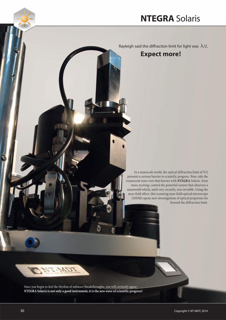
In a nanoscale world, the optical diffraction limit of /2 presents a serious barrier to scientific progress. Now, ride the
evanescent wave over that barrier with NTEGRA Solaris. Even more exciting: control the powerful system that observes a
nanoworld which, until very recently, was invisible. Using the near-field effect, this scanning near-field optical microscope
(SNOM) opens new investigations of optical properties far beyond the diffraction limit.
Rayleigh said the diffraction limit for light was /2.
Expect more!
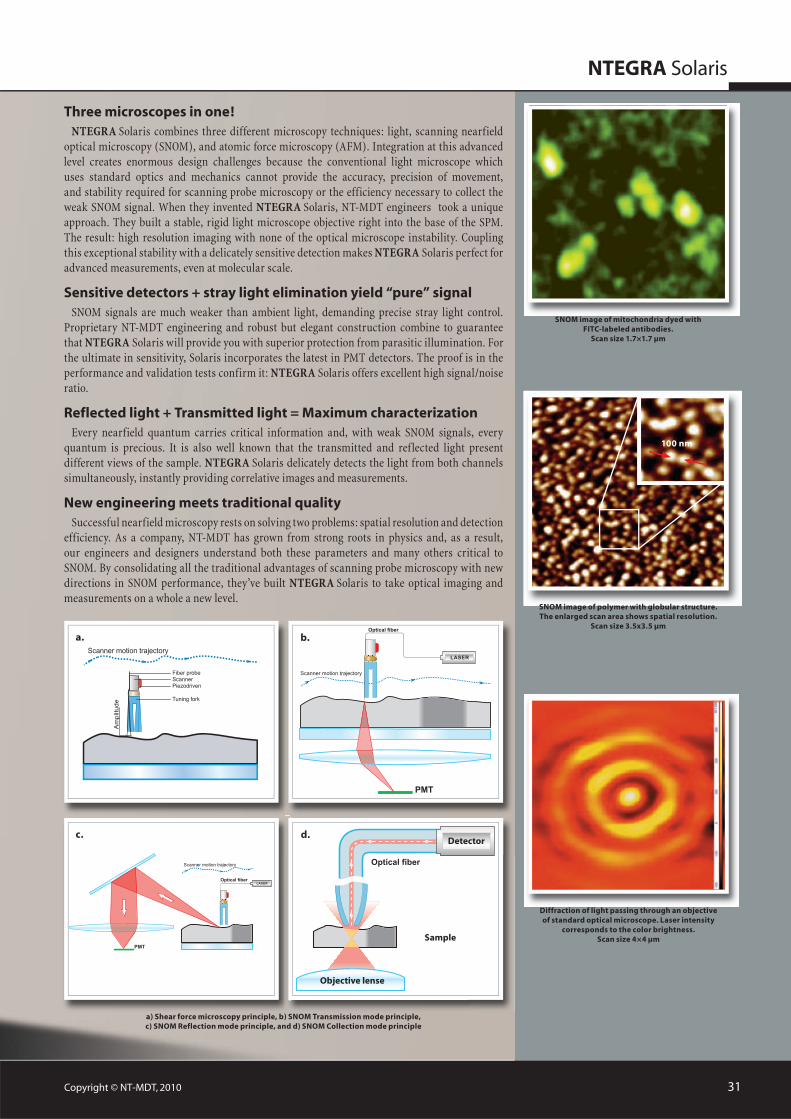
SNOM image of mitochondria dyed with FITC-labeled antibodies.
Scan size 1.7×1.7 µm
Diffraction of light passing through an objective of standard optical microscope. Laser intensity
corresponds to the color brightness. Scan size 4×4 µm
SNOM image of polymer with globular structure.The enlarged scan area shows spatial resolution.
Scan size 3.5x3.5 µm
a) Shear force microscopy principle, b) SNOM Transmission mode principle,c) SNOM Reflection mode principle, and d) SNOM Collection mode principle
a.
c. d.
100 nm
NTEGRA Solaris
b.
Copyright © NT-MDT, 2010 31
Three microscopes in one!NTEGRA Solaris combines three different microscopy techniques: light, scanning nearfield
optical microscopy (SNOM), and atomic force microscopy (AFM). Integration at this advanced level creates enormous design challenges because the conventional light microscope which uses standard optics and mechanics cannot provide the accuracy, precision of movement, and stability required for scanning probe microscopy or the efficiency necessary to collect the weak SNOM signal. When they invented NTEGRA Solaris, NT-MDT engineers took a unique approach. They built a stable, rigid light microscope objective right into the base of the SPM. The result: high resolution imaging with none of the optical microscope instability. Coupling this exceptional stability with a delicately sensitive detection makes NTEGRA Solaris perfect for advanced measurements, even at molecular scale.
Sensitive detectors + stray light elimination yield “pure” signalSNOM signals are much weaker than ambient light, demanding precise stray light control.
Proprietary NT-MDT engineering and robust but elegant construction combine to guarantee that NTEGRA Solaris will provide you with superior protection from parasitic illumination. For the ultimate in sensitivity, Solaris incorporates the latest in PMT detectors. The proof is in the performance and validation tests confirm it: NTEGRA Solaris offers excellent high signal/noise ratio.
Reflected light + Transmitted light = Maximum characterizationEvery nearfield quantum carries critical information and, with weak SNOM signals, every
quantum is precious. It is also well known that the transmitted and reflected light present different views of the sample. NTEGRA Solaris delicately detects the light from both channels simultaneously, instantly providing correlative images and measurements.
New engineering meets traditional qualitySuccessful nearfield microscopy rests on solving two problems: spatial resolution and detection
efficiency. As a company, NT-MDT has grown from strong roots in physics and, as a result, our engineers and designers understand both these parameters and many others critical to SNOM. By consolidating all the traditional advantages of scanning probe microscopy with new directions in SNOM performance, they’ve built NTEGRA Solaris to take optical imaging and measurements on a whole a new level.
Copyright © NT-MDT, 201032
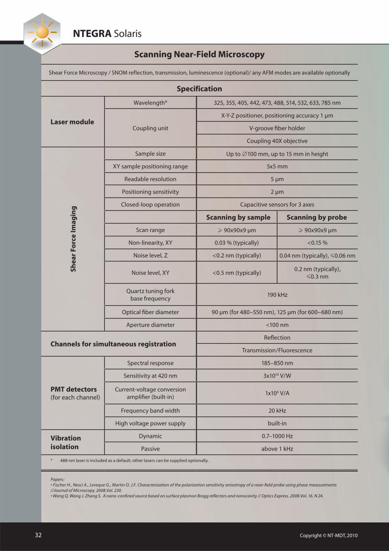
Scanning Near-Field Microscopy
Shear Force Microscopy / SNOM reflection, transmission, luminescence (optional)/ any AFM modes are available optionally
Specification
Laser module
Wavelength* 325, 355, 405, 442, 473, 488, 514, 532, 633, 785 nm
Coupling unit
X-Y-Z positioner, positioning accuracy 1 µm
V-groove fi ber holder
Coupling 40X objective
Shea
r Fo
rce
Imag
ing
Sample size Up to 100 mm, up to 15 mm in height
XY sample positioning range 5x5 mm
Readable resolution 5 µm
Positioning sensitivity 2 µm
Closed-loop operation Capacitive sensors for 3 axes
Scanning by sample Scanning by probe
Scan range � 90x90x9 µm � 90x90x9 µm
Non-linearity, XY 0.03 % (typically) <0.15 %
Noise level, Z <0.2 nm (typically) 0.04 nm (typically), �0.06 nm
Noise level, XY <0.5 nm (typically)0.2 nm (typically),
�0.3 nm
Quartz tuning forkbase frequency
190 kHz
Optical fi ber diameter 90 µm (for 480–550 nm), 125 µm (for 600–680 nm)
Aperture diameter <100 nm
Channels for simultaneous registrationRefl ection
Transmission/Fluorescence
PMT detectors (for each channel)
Spectral response 185–850 nm
Sensitivity at 420 nm 3x10¹⁰ V/W
Current-voltage conversion amplifi er (built-in)
1x10⁶ V/A
Frequency band width 20 kHz
High voltage power supply built-in
Vibration isolation
Dynamic 0.7–1000 Hz
Passive above 1 kHz
* 488 nm laser is included as a default; other lasers can be supplied optionally.
Papers:• Fischer H., Nesci A., Leveque G., Martin O. J.F. Characterization of the polarization sensitivity anisotropy of a near-fi eld probe using phase measurements //Journal of Microscopy. 2008.Vol. 230.• Wang Q. Wang J. Zhang S. A nano-confi ned source based on surface plasmon Bragg refl ectors and nanocavity // Optics Express. 2008.Vol. 16. N 24.
NTEGRA Solaris
NTEGRA Vita
Live and delicate
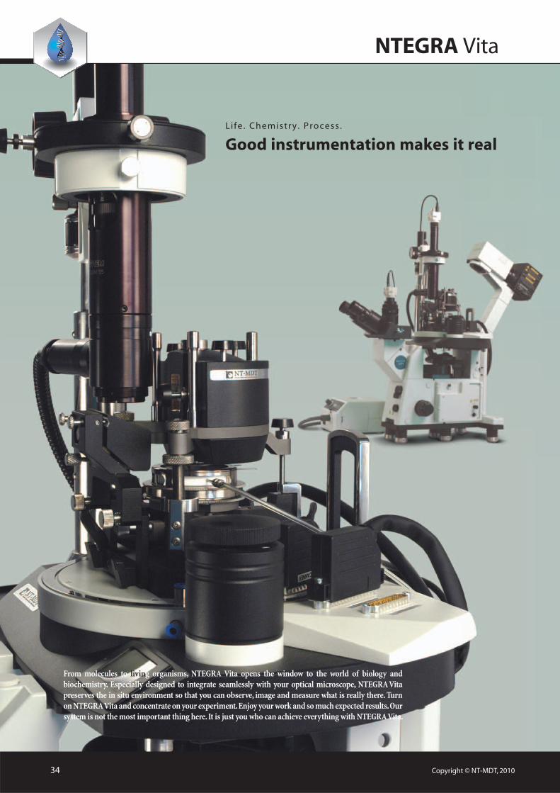
NTEGRA Vita
From molecules to living organisms, NTEGRA Vita opens the window to the world of biology and biochemistry. Especially designed to integrate seamlessly with your optical microscope, NTEGRA Vita preserves the in situ environment so that you can observe, image and measure what is really there. Turn on NTEGRA Vita and concentrate on your experiment. Enjoy your work and so much expected results. Our system is not the most important thing here. It is just you who can achieve everything with NTEGRA Vita.
Li fe . Chemistry . Process .
Good instrumentation makes it real
Copyright © NT-MDT, 201034
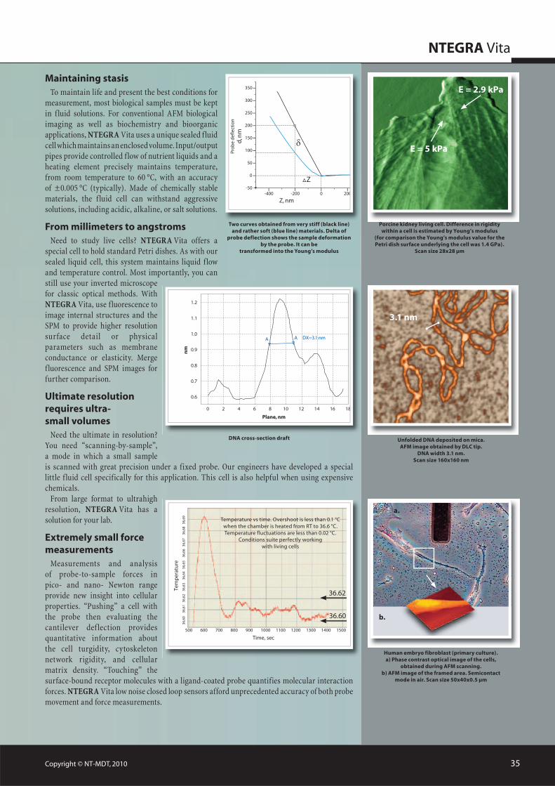
Maintaining stasisTo maintain life and present the best conditions for
measurement, most biological samples must be kept in f luid solutions. For conventional AFM biological imaging as well as biochemistry and bioorganic applications, NTEGRA Vita uses a unique sealed f luid cell which maintains an enclosed volume. Input/output pipes provide controlled f low of nutrient liquids and a heating element precisely maintains temperature, from room temperature to 60 °C, with an accuracy of ±0.005 °C (typically). Made of chemically stable materials, the f luid cell can withstand aggressive solutions, including acidic, alkaline, or salt solutions.
From millimeters to angstromsNeed to study live cells? NTEGRA Vita offers a
special cell to hold standard Petri dishes. As with our sealed liquid cell, this system maintains liquid f low and temperature control. Most importantly, you can still use your inverted microscope for classic optical methods. With NTEGRA Vita, use f luorescence to image internal structures and the SPM to provide higher resolution surface detail or physical parameters such as membrane conductance or elasticity. Merge f luorescence and SPM images for further comparison.
Ultimate resolution requires ultra-small volumes
Need the ultimate in resolution? You need “scanning-by-sample”, a mode in which a small sample is scanned with great precision under a fixed probe. Our engineers have developed a special little f luid cell specifically for this application. This cell is also helpful when using expensive chemicals.
From large format to ultrahigh resolution, NTEGRA Vita has a solution for your lab.
Extremely small force measurements
Measurements and analysis of probe-to-sample forces in pico- and nano- Newton range provide new insight into cellular properties. “Pushing” a cell with the probe then evaluating the cantilever def lection provides quantitative information about the cell turgidity, cytoskeleton network rigidity, and cellular matrix density. “Touching” the surface-bound receptor molecules with a ligand-coated probe quantifies molecular interaction forces. NTEGRA Vita low noise closed loop sensors afford unprecedented accuracy of both probe movement and force measurements.
NTEGRA Vita
Human embryo fibroblast (primary culture).a) Phase contrast optical image of the cells,
obtained during AFM scanning.b) AFM image of the framed area. Semicontact
mode in air. Scan size 50x40x0.5 µm
a.
b.
3.1 nm
Two curves obtained from very stiff (black line) and rather soft (blue line) materials. Delta of
probe deflection shows the sample deformation by the probe. It can be
transformed into the Young’s modulus
Unfolded DNA deposited on mica. AFM image obtained by DLC tip.
DNA width 3.1 nm.Scan size 160x160 nm
DNA cross-section draft
Porcine kidney living cell. Difference in rigidity within a cell is estimated by Young’s modulus
(for comparison the Young’s modulus value for the Petri dish surface underlying the cell was 1.4 GPa).
Scan size 28x28 µm
Temperature vs time. Overshoot is less than 0.1 °C when the chamber is heated from RT to 36.6 °C. Temperature fluctuations are less than 0.02 °C.
Conditions suite perfectly working with living cells
500 800 900 1000 140013001100 15001200700600
36,6
036
,62
36,6
336
,64
36,6
536
,66
36,6
736
,68
36,6
936
,61
Time, sec
Tem
per
atu
re
36.60
36.62
E = 5 kPa
E = 2.9 kPa
Copyright © NT-MDT, 2010 35
NTEGRA Vita
Scanning probe microscopy
SPM methods
in air & liquid
AFM (contact + semi-contact + non-contact) / Lateral Force Microscopy / Adhesion Force
Imaging/ Force Modulation/ Phase Imaging/ AFM Lithography (scratching)/ Force-Distance curves
in air only
STM/ Magnetic Force Microscopy/ Electrostatic Force Microscopy / Scanning Capacitance Microscopy/ Kelvin
Probe Microscopy/ Spreading Resistance Imaging/ Lithography: AFM (Current), STM
Scanning by sample Scanning by probe*
Sample size in airUp to 40 mm, up to
15 mm in height Up to 100 mm, up to
15 mm in height
in liquid Up to 14x14x2.5 mm Up to 15x15x3 mm
XY sample positioning rangein air 5x5 mm, 5 µm readable resolution, 2 µm sensitivity
in liquid 1x1 mm, 5 µm readable resolution, 2 µm sensitivity
Scan range � 90x90x9 µm � 90x90x9 µm
Non-linearity, XY(with closed-loop sensors***)
<0.1% <0.15%
Noise level, Z (RMS in bandwidth 1000Hz)
With sensors 0.04 nm (typically), �0.06 nm 0.06 nm (typically), �0.07 nm
Without sensors 0.03 nm 0.05 nm
Noise level, XY**(RMS in bandwidth 200 Hz)
With sensors0.2 nm (typically),
�0.3 nm (XY 100 µm)0.1 nm (typically),
�0.2 nm
Without sensors0.02 nm (XY 100 µm)0.001 nm (XY 3 µm)
0.01 nm
Temperature control(For operation in fl uid environment)
Range —from -10 °C to +60 °C for liquidfrom -30°C to +120 °C for gas
Stability — ±0.005 °C (typically), �±0.01 °C
* Scanning head can be configured to serve as a stand-alone device for specimens of unlimited sizes.** Built-in capacitive sensors have extremely low noise and any area down to 50x50 nm can be scanned with closed-loop control.
Optical microscopy*
Upright viewing Inverted viewingScanning by probe Scanning by sample Scanning by probe
Objective lens Magnifi cation x1/ x10 x1 x60**
Numerical aperture 0.1/ 0.28 0.1 0.7
Continuous zoom available NA
Observation methods***
Bright fi eld imaging available available
Fluorescence imaging NA optional
Contrast methodsPhase contrast imaging,
Polarization, DICNA optional
* System upgrade is possible to convert it into a near-field optical microscope or a laser confocal microscope.** Any additional objectives can be supplied optionally.*** Can be performed without compromise in optical or AFM performance.
Papers:• Risveden K., Ponten J.F., Calander N., Willander M., Danielsson B. The region ion sensitive fi eld effect transistor, a novel bioelectronic nanosensor // Biosensors and Bioelectronics. 2007. N 22.
Copyright © NT-MDT, 201036
NTEGRA Tomo
From flat slice to volume knowledge
NTEGRA Tomo
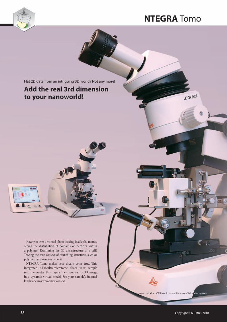
Have you ever dreamed about looking inside the matter, seeing the distribution of domains or particles within a polymer? Examining the 3D ultrastructure of a cell? Tracing the true context of branching structures such as polyurethane forms or nerves?
NTEGRA Tomo makes your dream come true. This integrated AFM/ultramicrotome slices your sample into nanometer thin layers then renders its 3D image in a dynamic virtual model. See your sample’s internal landscape in a whole new context.
Image of Leica EM UC6 Ultramicrotome. Courtesy of Leica Microsystems
38 Copyright © NT-MDT, 2010
Flat 2D data from an intriguing 3D world? Not any more!
Add the real 3rd dimension to your nanoworld!
NTEGRA Tomo
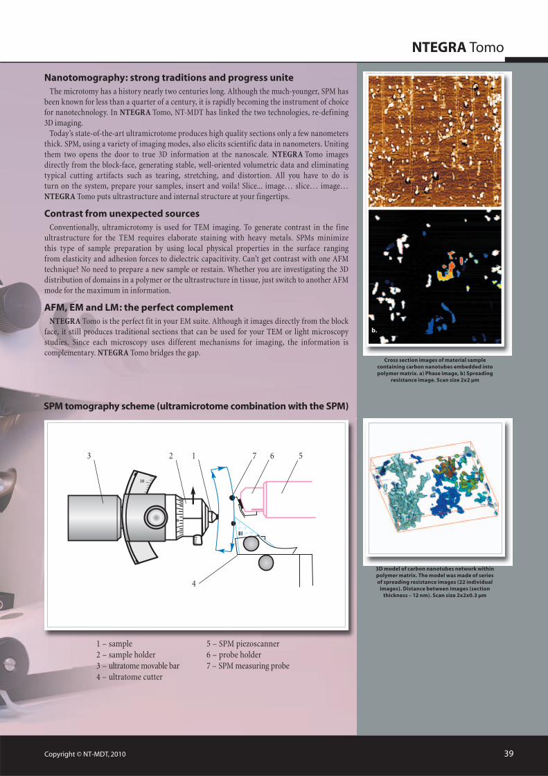
Cross section images of material sample containing carbon nanotubes embedded into polymer matrix. a) Phase image, b) Spreading
resistance image. Scan size 2x2 µm
1 – sample2 – sample holder3 – ultratome movable bar4 – ultratome cutter
SPM tomography scheme (ultramicrotome combination with the SPM)
5 – SPM piezoscanner6 – probe holder7 – SPM measuring probe
3
4
2 1 7 6 5
3D model of carbon nanotubes network within polymer matrix. The model was made of series of spreading resistance images (22 individual
images). Distance between images (section thickness – 12 nm). Scan size 2x2x0.3 µm
b.
a.
Copyright © NT-MDT, 2010 39
Nanotomography: strong traditions and progress uniteThe microtomy has a history nearly two centuries long. Although the much-younger, SPM has
been known for less than a quarter of a century, it is rapidly becoming the instrument of choice for nanotechnology. In NTEGRA Tomo, NT-MDT has linked the two technologies, re-defining 3D imaging.
Today’s state-of-the-art ultramicrotome produces high quality sections only a few nanometers thick. SPM, using a variety of imaging modes, also elicits scientific data in nanometers. Uniting them two opens the door to true 3D information at the nanoscale. NTEGRA Tomo images directly from the block-face, generating stable, well-oriented volumetric data and eliminating typical cutting artifacts such as tearing, stretching, and distortion. All you have to do is turn on the system, prepare your samples, insert and voila! Slice... image… slice… image… NTEGRA Tomo puts ultrastructure and internal structure at your fingertips.
Contrast from unexpected sourcesConventionally, ultramicrotomy is used for TEM imaging. To generate contrast in the fine
ultrastructure for the TEM requires elaborate staining with heavy metals. SPMs minimize this type of sample preparation by using local physical properties in the surface ranging from elasticity and adhesion forces to dielectric capacitivity. Can’t get contrast with one AFM technique? No need to prepare a new sample or restain. Whether you are investigating the 3D distribution of domains in a polymer or the ultrastructure in tissue, just switch to another AFM mode for the maximum in information.
AFM, EM and LM: the perfect complement NTEGRA Tomo is the perfect fit in your EM suite. Although it images directly from the block
face, it still produces traditional sections that can be used for your TEM or light microscopy studies. Since each microscopy uses different mechanisms for imaging, the information is complementary. NTEGRA Tomo bridges the gap.
NTEGRA Tomo
Scanning probe microscopy
in-situ: AFM (contact + semi-contact + non-contact) / Lateral Force Microscopy / Phase Imaging/Force Modulation/ Adhesion Force Imaging/ Magnetic Force Microscopy/ Electrostatic Force Microscopy / Scanning Capacitance Microscopy/
Kelvin Probe Microscopy/ Spreading Resistance Imaging/ Lithography: AFM (Force and Current)
Sample size 10x5x5 mm
Sample weight Up to 10 g
Scan range 100x100x10 µm
Positioning resolution 5 µm
Non-linearity, XY <0.15%
Noise level, Z (RMS in bandwidth 1000 Hz)
0.06 nm (typically), �0.07 nm
Noise level, XY(RMS in bandwidth 200 Hz)
0.2 nm (typically), �0.3 nm
Vibration isolationDynamic Frequency range 0.7–1000 Hz
Passive For frequencies above 1 kHz
Self locking Yes
Graduation ±30° graduation
Clearance angleadjustment
-2° to 15° with 1°scale
Knife holder For 6–12 mm knives
Coarse knife-movements
N-S 10 mm stepping motor
E-W 25 mm stepping motor
Cutting window 0.2–15 mm adjustable
Cutting speed 0.05–100 mm/s wheel contr.
Section thickness 0–15000 nm wheel contr.
FEED / SPEED storage 5
Return speeds 10, 30, 50 mm/s
Step control 0.1–15 µm steps
Section counter Yes
Feed totalizer Yes
Count down Yes
Rocking mode Yes
E-W measurement Yes
Auto trim Yes
Specimen advance indicator Yes
Working distance 110 mm
Universal specimen holder 2 pcs.
Flat specimen holder 1p.
Instrument table
Dimensions 0.67 x 1.15 m
Shock-absorbing elements
Yes
Ultratomy
Papers:• Efi mov A.E., Tonevitsky A.G., Dittrich M., Matsko N.B. Atomic force microscope (AFM) combined with the ultramicrotome: a novel device for the serial section tomography and AFM/TEM complementary structural analysis of biological and polymer samples // Journal of Microscopy. 2007. Vol. 226, pp. 207–217.
Copyright © NT-MDT, 201040
NTEGRA Spectra
Color the nanoworld
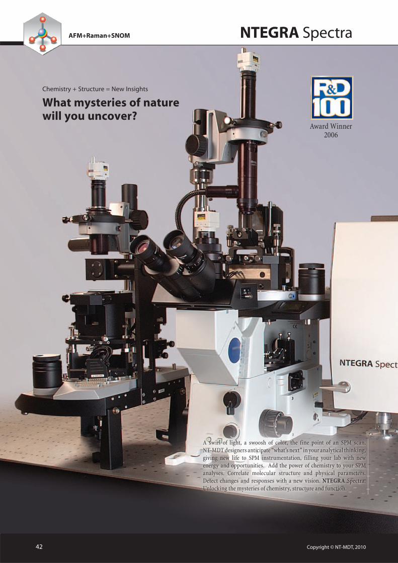
NTEGRA Spectra
A swirl of light, a swoosh of color, the fine point of an SPM scan. NT-MDT designers anticipate “what’s next” in your analytical thinking, giving new life to SPM instrumentation, filling your lab with new energy and opportunities. Add the power of chemistry to your SPM analyses. Correlate molecular structure and physical parameters. Detect changes and responses with a new vision. NTEGRA Spectra. Unlocking the mysteries of chemistry, structure and function.
Chemistry + Structure = New Insights
What mysteries of nature will you uncover?
Award Winner2006
AFM+Raman+SNOM
42 Copyright © NT-MDT, 2010
NTEGRA Spectra
Confocal Raman: imaging and spectroscopy
Confocal fluorescence: imaging and spectroscopy
Atomic-force microscopy: mechanical, electrical, magnetic properties
and nanomanipulations
Near-field optical microscopy
Optical microscopy and laser confocal imaging
All techniques can be applied to the same object. Measurements in air, liquids, gases with controlled temperature and humidity.
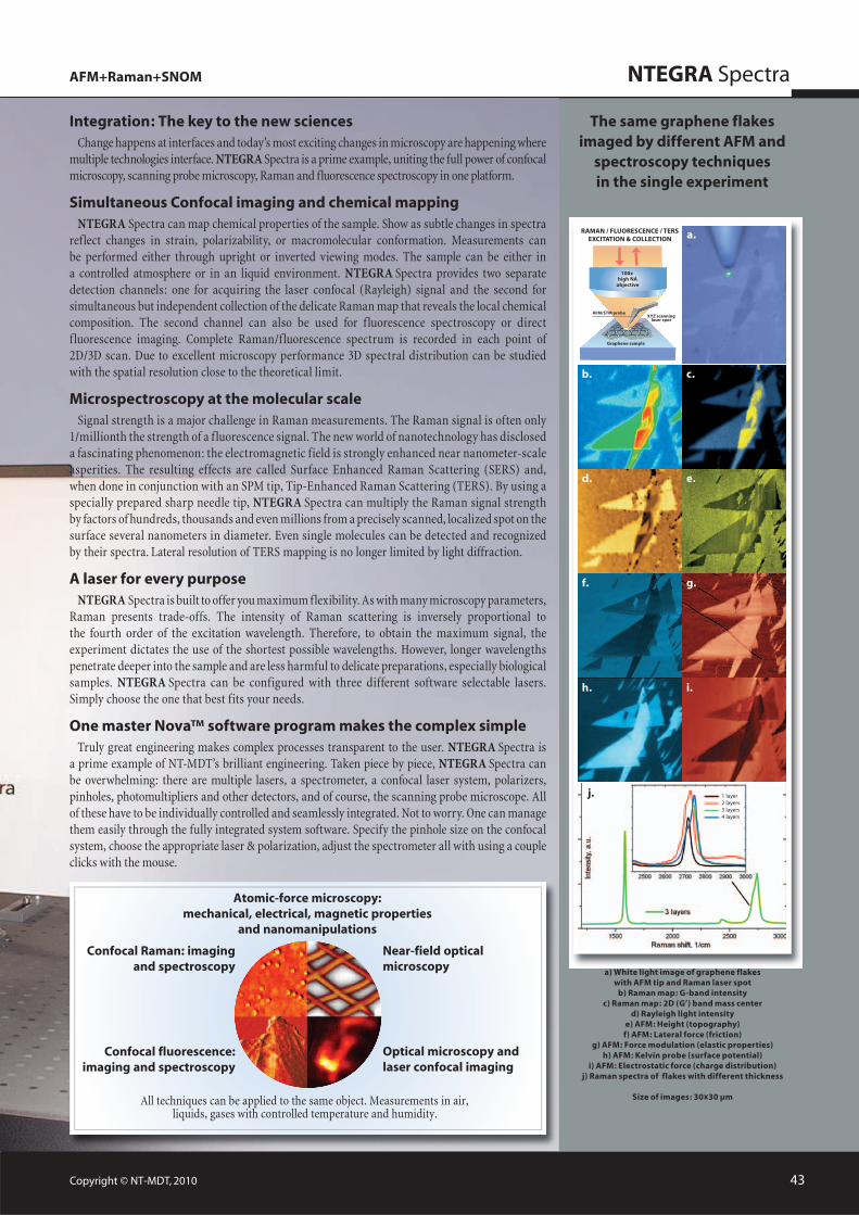
a) White light image of graphene flakes with AFM tip and Raman laser spot
b) Raman map: G-band intensityc) Raman map: 2D (G’) band mass center
d) Rayleigh light intensitye) AFM: Height (topography)
f) AFM: Lateral force (friction)g) AFM: Force modulation (elastic properties)
h) AFM: Kelvin probe (surface potential)i) AFM: Electrostatic force (charge distribution)
j) Raman spectra of flakes with different thickness
Size of images: 30x30 µm
The same graphene flakes imaged by different AFM and
spectroscopy techniques in the single experiment
AFM+Raman+SNOM
43Copyright © NT-MDT, 2010
b. c.
d. e.
f. g.
h. i.
j.
a.
1 layer2 layers3 layers4 layers
RAMAN / FLUORESCENCE / TERS EXCITATION & COLLECTION
AFM/STM probe
Graphene sample
100x high NA
objective
XYZ scanning laser spot
a.
Integration: The key to the new sciences Change happens at interfaces and today’s most exciting changes in microscopy are happening where
multiple technologies interface. NTEGRA Spectra is a prime example, uniting the full power of confocal microscopy, scanning probe microscopy, Raman and fluorescence spectroscopy in one platform.
Simultaneous Confocal imaging and chemical mapping NTEGRA Spectra can map chemical properties of the sample. Show as subtle changes in spectra
reflect changes in strain, polarizability, or macromolecular conformation. Measurements can be performed either through upright or inverted viewing modes. The sample can be either in a controlled atmosphere or in an liquid environment. NTEGRA Spectra provides two separate detection channels: one for acquiring the laser confocal (Rayleigh) signal and the second for simultaneous but independent collection of the delicate Raman map that reveals the local chemical composition. The second channel can also be used for fluorescence spectroscopy or direct fluorescence imaging. Complete Raman/fluorescence spectrum is recorded in each point of 2D/3D scan. Due to excellent microscopy performance 3D spectral distribution can be studied with the spatial resolution close to the theoretical limit.
Microspectroscopy at the molecular scaleSignal strength is a major challenge in Raman measurements. The Raman signal is often only
1/millionth the strength of a f luorescence signal. The new world of nanotechnology has disclosed a fascinating phenomenon: the electromagnetic field is strongly enhanced near nanometer-scale asperities. The resulting effects are called Surface Enhanced Raman Scattering (SERS) and, when done in conjunction with an SPM tip, Tip-Enhanced Raman Scattering (TERS). By using a specially prepared sharp needle tip, NTEGRA Spectra can multiply the Raman signal strength by factors of hundreds, thousands and even millions from a precisely scanned, localized spot on the surface several nanometers in diameter. Even single molecules can be detected and recognized by their spectra. Lateral resolution of TERS mapping is no longer limited by light diffraction.
A laser for every purposeNTEGRA Spectra is built to offer you maximum flexibility. As with many microscopy parameters,
Raman presents trade-offs. The intensity of Raman scattering is inversely proportional to the fourth order of the excitation wavelength. Therefore, to obtain the maximum signal, the experiment dictates the use of the shortest possible wavelengths. However, longer wavelengths penetrate deeper into the sample and are less harmful to delicate preparations, especially biological samples. NTEGRA Spectra can be configured with three different software selectable lasers. Simply choose the one that best fits your needs.
One master Nova™ software program makes the complex simpleTruly great engineering makes complex processes transparent to the user. NTEGRA Spectra is
a prime example of NT-MDT’s brilliant engineering. Taken piece by piece, NTEGRA Spectra can be overwhelming: there are multiple lasers, a spectrometer, a confocal laser system, polarizers, pinholes, photomultipliers and other detectors, and of course, the scanning probe microscope. All of these have to be individually controlled and seamlessly integrated. Not to worry. One can manage them easily through the fully integrated system software. Specify the pinhole size on the confocal system, choose the appropriate laser & polarization, adjust the spectrometer all with using a couple clicks with the mouse.
NTEGRA Spectra
RAMAN / FLUORESCENCE / TERS EXCITATION & COLLECTION
XYZ scanning
stage
XYZ scanning AFM/STM probe
Laser spot
AFM/STM probe
RAMAN / FLUORESCENCE / TERS EXCITATION & COLLECTION
100x high NA
objective
100x high NA
objective
RAMAN / FLUORESCENCE / TERS EXCITATION & COLLECTION
TERS EXCITATION/COLLECTION
100x high NA
objective
AFM/STM probe
XYZ scanning laser spot
XYZ scanning laser spot1 AFM probe and laser beam are perfectly coordinated with each other. The AFM probe
can be placed within the laser spot with nanometer precision — as it is necessary for tip-enhanced optical effects. Movement in 6 different axes is controlled by closed-loop sensors.2 High NA objective is rigidly integrated into the SPM base. It provides unprecedented
optical system stability — designed for long-term and weak-signal experiments.3 Reflected laser light is used to obtain fast confocal laser (Rayleigh) image.4 TE-cooled (down to -100°C) CCD or EMCCD serves as a sensitive spectroscopy detector. Alternatively
avalanche photodiode or photon multiplier (PMT) can be used for single photon counting.5 Flexible polarization optics in both excitation and detection channels. User defined optical filters. All
motorized, software controlled.6 Excellent software integration has been realized. All system modules (AFM, optics and mechanics) are
driven by the same software package. Lasers, gratings, polarizers, pinholes etc, can be chosen and adjusted from the program.7 AFM and confocal Raman maps are acquired simultaneously and analyzed in the same software package8 Solutions for all possible TERS geometries. Dual scan option: scan by sample plus scan by tip / by laser
beam
NTEGRA Spectra optical scheme
Inverted setup:
• Optimized for transparent samples• Highest optical resolution achievable (<200 nm) simultaneously with AFM• Highest efficiency of Raman/fluorescence Photon collection (with immersion optics) simultaneously with AFM• Probe scanning in addition to sample scanning (important for TERS)• Equipped with heating stage, temperature controlled liquid cell and environmental chamber• Fits most commercial inverted microscopes, supporting advanced imaging modes
Upright setup:
• Optimized for opaque samples• Highest optical resolution (400 nm) simultaneously with AFM• Highest efficiency of Raman/Fluorescence photon collection simultaneously with AFM• Beam scanning in addition to sample scanning (necessary for TERS)• Equipped with heating stage, environmental chamber
4
3
2
16 5
1
AFM+Raman+SNOM
8
8
8
a) Based on quartz SNOM fiber, shear-force feedback.b) Based on silicon cantilevers with
nanofabricated aperture
7
b.
a.
SNOM
Work both with cantilevers (contact, intermittent contact and other modes: more than 30) and with metal tips (STM mode, shear force mode, normal force mode)
Spectrometer
Confocal module
Copyright © NT-MDT, 201044
NTEGRA Spectra
Tip approached
Tip retracted
a) A specially prepared AFM probe (metal coated cantilever or etched metal wire) is precisely positioned inside a tightly focused laser spot. b) Intensity of carbon nanotube G- and D- Raman bands increases by several orders of magnitude when the special AFM probe is landed and positioned over a small (5 nm height) nanotube bundle — the effect of Tip Enhanced Raman Scattering (TERS). c) “Conventional” confocal Raman image of the nanotube bundle, the observed width of the bundle is ~250 nm (diffraction limit of confocal microscopy, laser
wavelength — 633 nm). d) TERS image of the same bundle – now the observed width is 50–70 nm.Note, in this example, TERS provides more than 4-times better spatial resolution as compared to confocal microscopy. Resolution down to 10 nm and less is theoretically possible. Measurements are done with NTEGRA Spectra in Inverted configuration.Data courtesy of Dr. S. Kharintsev, Dr. J. Loos, Dr. G. Hoffmann, Prof. G. de With, TUE, the Netherlands and Dr. P. Dorozhkin, NT-MDT Co.
c. d.a.
1000 20001500 cm-1
b.
Focused laser spot
Enhanced Raman signal
AFM probe
Raman microscopy with ultra-high spatial resolution
200 nm200 nm
5 µm 5 µm5 µm
a. b. c. d.
Fluorescent nanowire is excited by 488 nm light at the body (left image) and at the left bottom end (right image). Excitation light is completely
cut off from the image by two edge filters (with 10-6 transmission). Part of the fluorescence light emitted from nanowire (>10%) is
transmitted through it and is emitted from nanowire ends
Light transport in nanostructures Stress mapping in silicon structures
Comprehensive analysis of biological structures
a) AFM topography of indentation in silicon substrate. b) Center of mass position shift of 520 cm-1 silicon line — proportional
to stress distribution around the indentation. Spectral resolution better then 0.1 cm-1
Excitation pointEmission from ends
Excitation point Emission from end
0.5 cm-1
2 µm
a. b.
Algal cells visualization by different techniques. a) Bright field overview. b) Confocal Raman map at 1524 cm-1 (beta-carotene line). c) Confocal image of autofluorescence at 492–513 nm. d) AFM image.
Sample courtesy of Don McNaughton, Monash University, Victoria, Australia
AFM+Raman+SNOM
Copyright © NT-MDT, 2010 45
NTEGRA Spectra
Copyright © NT-MDT, 201046
Confocal Raman/Fluorescence microscopy
Confocal Raman/Fluorescence/Rayleigh imaging runs simultaneously with AFM (during one sample scan)
Diffraction limited spatial resolution: <200 nm in XY, <500 nm in Z (with immersion objective)
True confocality; motorized confocal pinhole for optimal signal and confocality
Motorized variable beam expander/collimator: adjusts diameter and collimation of the laser beam individually for each laser and each objective used
Full 3D (XYZ) confocal imaging with powerful image analysis
Hyperspectral imaging (recording complete Raman spectrum in every point of 1D, 2D or 3D confocal scan) with further software analysis
Optical lithography (vector, raster)
AFM/STM: Integration with spectroscopy
Upright and Inverted optical AFM configurations (optimized for opaque and transparent samples correspondingly); side illumination option
Highest possible resolution (numerical aperture) optics is used simultaneously with AFM: 0.7 NA for Upright, 1.3–1.4 NA for Inverted
AFM/STM and confocal Raman/Fluorescence images are obtained simultaneously (during one scan)
All standard SPM imaging modes are supported (>30 modes) — combined with confocal Raman/Fluorescence
Low noise AFM/STM (atomic resolution)
Vibrations and thermal drifts originating from optical microscope body are minimized due to special design of optical AFM heads
Focus track feature: sample always stays in focus due to AFM Z-feedback; high quality confocal images of very rough or inclined samples can be obtained
Software
Seamless integration of AFM and Raman; all AFM/Raman/SNOM experiment and further data analysis is performed in one and the same software
Powerful analysis of 1D, 2D and 3D hyperspectral images
Powerful export to other software (Excel, MatLab, Cytospec etc.)
Spectroscopy*
Extremely high efficiency 520 mm length spectrometer with 4 motorized gratings
Visible, UV and IR spectral ranges available
Echelle grating with ultrahigh dispersion; spectral resolution: 0.007 nm (< 0.1 1/cm)**
Up to 3 different detectors can be installed- TE cooled (down to -100 ºC) CCD camera. EMCCD camera is optional — for ultrafast imaging- Photon multiplier (PMT) or avalanche photodiode in photon counting mode- Photon multiplier for fast confocal laser (Rayleigh) imaging
Flexible motorized polarization optics in excitation and detection channels, cross-polarized Raman measurements
Fully automated switch between different lasers — with a few mouse clicks
Scanning Near Field Optical Microscopy(SNOM)
Two major SNOM techniques supported: (i) based on quartz fiber probes, (ii) based on silicon cantilever probes
All modes supported: Transmission, Collection, Reflection
All SNOM signals detected: laser intensity, fluorescence intensity, spectroscopy
SNOM lithography (vector, raster)
Optimized for Tip Enhanced Raman Scattering (TERS) and other tip-related optical techniques (S-SNOM, TEFS, STM-LE etc.)
All existing TERS geometries are available: illumination/collection from bottom, from top or from side
Different SPM techniques and TERS probes can be used: STM, AFM cantilever, quartz tuning fork in tapping and shear force modes
Dual scan (for Hot Point Mapping in TERS): scan by sample AND scan by tip / by laser spot
Motorized polarization optics to produce optimal polarization for TERS
AFM-Raman measurements can run in air, in controlled atmosphere or in liquid — all with variable temperature
Some features listed are optional — not included into basic system configuration
* NT-MDT AFM can be integrated with Renishaw inVia or with NT-MDT spectrometer. Specifications are given for the latter.
Renishaw specifications can be found at www.renishaw.com/AFM-Raman
** Exact value of spectral resolution highly depends on how “resolution” is defined
Copyright © NT-MDT, 2010 47
NanoindentationAny NTEGRA based system can be supplied with the TriboScope® nanomechanical test
instrument. The TriboScope® utilizes an in-situ imaging capability to realize the benefits of SPM imaging and nanoindentation in a single system.
The TriboScope® combines nanoNewton force sensitivity and picometer displacement resolution with SPM imaging for a powerful tool to aid in material studies from basic research to product development to quality control.
TriboScope® is a registered trademark of the Hysitron Inc. company.
NTEGRA Spectra + Renishaw Raman microscope = Real integrationNT-MDT, a world-known manufacturer of scanning probe microscopes, and Renishaw, a world-
known manufacturer of Raman microscopes, joined their efforts in creation of the fascinating scientific instrument for comprehensive surface analysis.
Only NTEGRA Spectra provides fully technical integrated with Renishaw spectrometer solution in terms of software, hardware, and concept for interdisciplinary science at the molecular level. As a result of such union, researcher can obtain optimum efficiency and more time for investigations which allow to focus on data collection and analysis. Real integration is better than just a combination.
Renishaw spectrometer is a product of the Renishaw plc.
The policy of NT-MDT is to provide the complete instrumentation compatibility with the world-famous manufacturers of SPM-associated devices
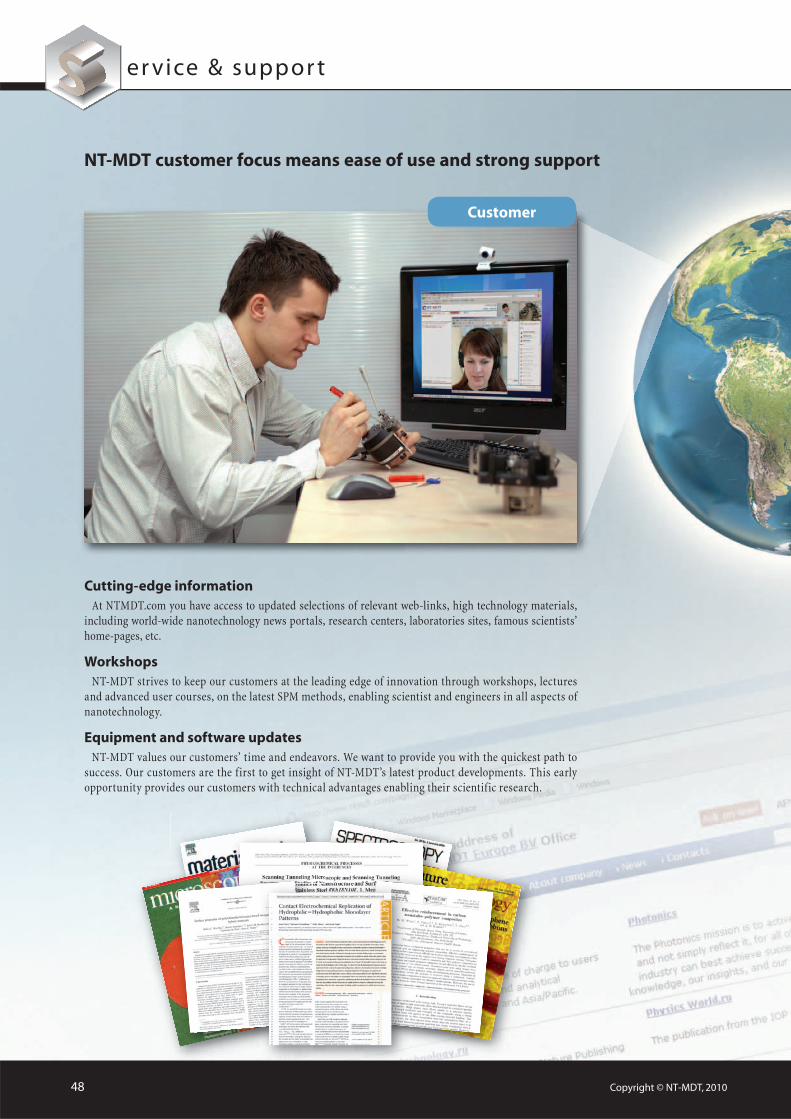
er vice & suppor t
Customer
Copyright © NT-MDT, 201048
Cutting-edge information At NTMDT.com you have access to updated selections of relevant web-links, high technology materials,
including world-wide nanotechnology news portals, research centers, laboratories sites, famous scientists’ home-pages, etc.
WorkshopsNT-MDT strives to keep our customers at the leading edge of innovation through workshops, lectures
and advanced user courses, on the latest SPM methods, enabling scientist and engineers in all aspects of nanotechnology.
Equipment and software updatesNT-MDT values our customers’ time and endeavors. We want to provide you with the quickest path to
success. Our customers are the first to get insight of NT-MDT’s latest product developments. This early opportunity provides our customers with technical advantages enabling their scientific research.
NT-MDT customer focus means ease of use and strong support

NT-MDT experts
Copyright © NT-MDT, 2010 49
World-wide service supportNT-MDT is a global company with a full service and support staff that allows us to care for our
customer regardless of their location. Wherever you are, you’re not far from help, please don’t hesitate to call on us for assistance.
Installation & periodical equipment diagnosticsEvery NT-MDT customer is a customer forever. Your equipment will be installed and you will
receive training from an NT-MDT expert. We will ensure that you understand all the basics to operate your new SPM properly.
Moreover, all NT-MDT SPM systems have integrated diagnostic tools. In case of an unexpected system failure it also eases the conversation with our technical assistance team. Upon your request a service engineer can easily examine your system remotely and carry out all necessary steps in order to ensure it is operating correctly.
Ask-online serviceNothing can be compared with personal conversation and sincere concern from professionals in
solving your problems. Ask-online system – expert consultation via Internet.For any problems and questions, urgent or not, we have a group of specialists standing by to assist
you via our unique Ask-online! It’s easy to get in touch with our experts.
Accessories on-lineNT-MDT manufactures a complete line of SPM accessories including wide range of probes, test
samples, and test gratings, all available on-line at www.ntmdt-tips.com.
Service and support
Information is subject to change without notice
Building 100, Zelenograd, Moscow 124482, RussiaPhone: +7 (499) 735-7777 Fax: +7 (499) 735-6410E-mail: [email protected]
NT-MDT Co.
High Tech Campus 835656 AG EindhovenThe NetherlandsPhone.: +31(0) 88 338 99 99Fax: +31(0) 88 338 99 98E-mail: [email protected]
NT-MDT Europe BV
NT-MDT House, National Technological ParkCastletroy, Limerick, IrelandPhone.: +353 (61) 33-33-22Fax: +353 (61) 33-33-20E-mail: [email protected]
NT-MDT Service & Logistics Ltd.
3200 Scott BlvdSanta Clara, CA 95054Phone: +1 408 988 8409Fax: +1 408 988 8442E-mail: [email protected]
NT-MDT America Inc.
Room 18D, Cross Region Plaze, No. 899 Lingling Road, Shanghai 200030, PRC Phone.: +86 21 5425 9595 Fax: +86 21 5425 0950 E-mail: [email protected]
NT-MDT Shanghai Representative Office
http://www.ntmdt.com/
I T ’ S T I M E F O R I N T E G R A T I O N !