Embed Size (px)
Citation preview
Application ReportJacinto 7 LPDDR4 Board Design and Layout Guidelines
ABSTRACT
This application report contains material applicable to the LPDDR4 interface of Jacinto7 processor board designs.
Table of Contents1 Overview..................................................................................................................................................................................3
1.1 Board Designs Supported.................................................................................................................................................. 31.2 General Board Layout Guidelines...................................................................................................................................... 31.3 PCB Stack-Up.................................................................................................................................................................... 41.4 Bypass Capacitors............................................................................................................................................................. 51.5 Velocity Compensation.......................................................................................................................................................6
2 LPDDR4 Board Design and Layout Guidance......................................................................................................................72.1 LPDDR4 Introduction......................................................................................................................................................... 72.2 LPDDR4 Device Implementations Supported.................................................................................................................... 72.3 LPDDR4 Interface Schematics.......................................................................................................................................... 72.4 Compatible JEDEC LPDDR4 Devices..............................................................................................................................112.5 Placement.........................................................................................................................................................................112.6 LPDDR4 Keepout Region................................................................................................................................................ 122.7 Net Classes......................................................................................................................................................................122.8 LPDDR4 Signal Termination............................................................................................................................................ 122.9 LPDDR4 VREF Routing................................................................................................................................................... 122.10 LPDDR4 VTT................................................................................................................................................................. 132.11 CK and ADDR_CTRL Topologies...................................................................................................................................132.12 Data Group Topologies.................................................................................................................................................. 142.13 CK and ADDR_CTRL Routing Specification..................................................................................................................152.14 Data Group Routing Specification..................................................................................................................................152.15 Channel, Byte, and Bit Swapping...................................................................................................................................16
3 LPDDR4 Board Design Simulations....................................................................................................................................173.1 Board Model Extraction....................................................................................................................................................173.2 Board-Model Validation.................................................................................................................................................... 173.3 S-Parameter Inspection................................................................................................................................................... 173.4 Time Domain Reflectometry (TDR) Analysis....................................................................................................................173.5 Simulation Integrity Analysis............................................................................................................................................ 193.6 Design Example............................................................................................................................................................... 24
4 Revision History................................................................................................................................................................... 29
List of FiguresFigure 2-1. 32-Bit, Single-Rank LPDDR4 Implementation...........................................................................................................8Figure 2-2. 32-Bit, Dual Rank LPDDR4 Implementation............................................................................................................. 9Figure 2-3. 16-Bit, Single Rank LPDDR4 Implementation.........................................................................................................10Figure 2-4. DRA829 / LPDDR4 Example Placement.................................................................................................................11Figure 2-5. Example LPDDR4 Keepout Region for DRA829.....................................................................................................12Figure 2-6. LPDDR4 CK Topology.............................................................................................................................................13Figure 2-7. LPDDR4 ADDR_CTRL Topology/Branched Signals............................................................................................... 13Figure 2-8. LPDDR4 ADDR_CTRL Topology/Point-to-Point Signals.........................................................................................13Figure 2-9. LPDDR4 DQS Topology.......................................................................................................................................... 14Figure 2-10. LPDDR4 DQ/DM Topology....................................................................................................................................14Figure 3-1. TDR Plot Example With Impedance Mismatch....................................................................................................... 18Figure 3-2. Typical System-Level DDR Schematic....................................................................................................................19Figure 3-3. Example of Ring-back Margin Waveforms (High/Low)............................................................................................21
www.ti.com Table of Contents
SPRACN9B – DECEMBER 2019 – REVISED AUGUST 2021Submit Document Feedback
Jacinto 7 LPDDR4 Board Design and Layout Guidelines 1
Copyright © 2021 Texas Instruments Incorporated
Figure 3-4. Vix_CK and Vix_DQS Ratio for Eye Quality............................................................................................................21Figure 3-5. Sample Simulated LPDDR4-4266 Read Eye With Diamond-Shaped Eye Mask.................................................... 23Figure 3-6. Sample Simulated LPDDR4-4266 Write Eye With Rectangular JEDEC Eye Mask................................................ 23Figure 3-7. Sample Simulated LPDDR4-4266 CA Eye With Rectangular JEDEC Eye Mask................................................... 24Figure 3-8. Example LPDDR4 Clock and CA Routing...............................................................................................................25Figure 3-9. Example LPDDR4 Data Byte(s) and DQS(s) Routing.............................................................................................25Figure 3-10. Example LPDDR4 Trace Impedance Scan........................................................................................................... 26Figure 3-11. LPDDR4 Simulation Results for CA.......................................................................................................................27Figure 3-12. LPDDR4 Simulation Results for Write...................................................................................................................28Figure 3-13. LPDDR4 Simulation Results for Read...................................................................................................................28
List of TablesTable 1-1. PCB Stack-up Specifications ..................................................................................................................................... 4Table 1-2. Bulk Bypass Capacitors.............................................................................................................................................. 5Table 1-3. High-Speed Bypass Capacitors.................................................................................................................................. 6Table 2-1. Supported LPDDR4 SDRAM Combinations............................................................................................................... 7Table 2-2. Compatible JEDEC LPDDR4 Devices...................................................................................................................... 11Table 2-3. LPDDR4 Placement Recommendations................................................................................................................... 11Table 2-4. Clock Net Class Definitions.......................................................................................................................................12Table 2-5. Signal Net Class Definitions......................................................................................................................................12Table 2-6. CK and ADDR_CTRL Routing Specifications...........................................................................................................15Table 2-7. Data Group Routing Specifications...........................................................................................................................16Table 3-1. Example Data Write ODI/ODT Optimization............................................................................................................. 20Table 3-2. Vix_CK and Vix_DQS Ratio for Eye Quality............................................................................................................. 21Table 3-3. LPDDR4/4x Eye Mask Definitions/Requirements..................................................................................................... 22Table 3-4. Example PCB Stackup for LPDDR4......................................................................................................................... 24Table 3-5. LPDDR4 Performance Impact from StackUp............................................................................................................25Table 3-6. LPDDR4 Performance Impact on Routing Layer...................................................................................................... 25Table 3-7. Example LPDDR4 Trace Impedance Summary for Data..........................................................................................26Table 3-8. Example LPDDR4 Trace Impedance Summary for CA............................................................................................ 26Table 3-9. Example LPDDR4 Simulation Results From Improved Trace Impedance................................................................27
TrademarksAll trademarks are the property of their respective owners.
Trademarks www.ti.com
2 Jacinto 7 LPDDR4 Board Design and Layout Guidelines SPRACN9B – DECEMBER 2019 – REVISED AUGUST 2021Submit Document Feedback
Copyright © 2021 Texas Instruments Incorporated

1 OverviewThe Jacinto7 processor supports the LPDDR4 memory interface. This allows customer board designs to reduce the power consumption of their memory system while at the same time, allowing extreme memory bandwidth to supply the heavy demands of the processor subsystem.
1.1 Board Designs SupportedThe goal of this document is to make the Jacinto7 LPDDR4 system implementation straightforward for all designers. Requirements have been distilled down to a set of layout and routing rules that allow designers to successfully implement a robust design for the topologies that TI supports. It is also required, especially at the higher rates, that the PCB design be simulated to ensure the design targets are achieved. Reference eye masks are provided as guidance for validation of the simulations results. At this time, TI does not provide timing parameters for the processor’s DDR PHY interface.
It is still expected that the PCB design work (design, layout, and fabrication) is performed and reviewed by a highly knowledgeable high-speed PCB designer. Problems such as impedance discontinuities when signals cross a split in a reference plane can be detected visually by those with the proper experience.
TI only supports board designs that follow the guidelines in this document. These guidelines are based on well-known transmission line properties for copper traces routed over a solid reference plane. Declaring insufficient PCB space does not allow routing guidelines to be discounted
1.2 General Board Layout GuidelinesTo ensure good signaling performance, the following general board design guidelines must be followed:
• All signals need ground reference (strongly suggest on both sides)• Avoid crossing plane splits in the signal reference planes.• Use the widest trace that is practical between decoupling capacitors and memory modules.• Minimize inter-symbol interference (ISI) by keeping impedances matched.• Minimize crosstalk by isolating sensitive signals, such as strobes and clocks, and by using a proper PCB
stack-up.• Avoid return path discontinuities by adding vias or capacitors whenever signals change layers and reference
planes.• Minimize reference voltage noise through proper isolation and proper use of decoupling capacitors on the
reference input pins on the SDRAMs.• Keep the signal routing stub lengths as short as possible.• Add additional spacing for clock and strobe nets to minimize crosstalk.• Maintain a common ground (also called VSS) reference for all bypass and decoupling capacitors.• Consider the differences in propagation delays between microstrip and stripline nets when evaluating timing
constraints.• Via-to-via coupling can be significant part of PCB-level crosstalk. Dimension and pitch of vias is important.
For high speed interfaces, consider GND shielding vias.• Via stubs affect signal integrity. Via back-drilling can improve signal integrity, and may be required in some
instances.
For more information, see the High-Speed Interface Layout Guidelines Application Report. It provides additional general guidance for successful routing of high-speed signals.
www.ti.com Overview
SPRACN9B – DECEMBER 2019 – REVISED AUGUST 2021Submit Document Feedback
Jacinto 7 LPDDR4 Board Design and Layout Guidelines 3
Copyright © 2021 Texas Instruments Incorporated

1.3 PCB Stack-UpThe recommended stack-up for routing the DDR interface is a ten layer stack up. However, this can only be accomplished on a board with routing room with large keep-out areas. Additional layers are required if:
• The PCB layout area for the DDR Interface is restricted, which limits the area available to spread out the signals to minimize crosstalk.
• Other circuitry must exist in the same area, but on layers isolated from the DDR routing.• Additional planes layers are needed to enhance the power supply routing or to improve EMI shielding.
Board designs that are relatively dense may require more layers to properly allow the DDR routing to be implemented such that all rules are met.
All DDR signals must be routed adjacent to a solid VSS reference plane. When multiple VSS reference planes exist in the DDR routing area, stitching vias must be implemented nearby wherever vias transfer signals to a different VSS reference plane. This is required to maintain a low-inductance return current path.
It is strongly recommended all DDR signals be routed as strip-line. Some PCB stack-ups implement signal routing on 2 adjacent layers. This is not recommended as crosstalk occurs on any trace routed parallel to another trace on an adjacent layer, even for a very short distance. It is recommended to route LPDDR4 signals on PCB layers closer to the SoC within the stackup, giving the signal a shorter travel time through the via. The PCB layers farther from the SoC will have longer travel times through the via, which can increase coupling between vias. Both signal and via coupling can lead to smaller timing margins.
Note a shorter via travel could mean a longer via stub (if using standard drill vias), so that needs to be considered as well. Simulation can be used to determine if via stub length is an issue.
PCB material is another important factor. Depending on the design specifics, it may be required to use a higher frequency material such as ISOLA I-Speed or equivalent/better to achieve highest data rates. Standard FR4 products like 370HR can be used for lower data rates. In specific cases, it is sufficient for higher data rates as well.
Table 1-1. PCB Stack-up Specifications Number Parameter(6) MIN TYP MAX UNIT
PS1 PCB routing plus plane layers 10
PS2 Signal routing layers 6
PS3 Full VSS reference layers under DDR routing region (1) 1
PS4 Full VDDS_DDR power reference layers under the DDR routing region (1) 1
PS5 Number of reference plane cuts allowed within DDR routing region (2) 0
PS6 Number of layers between DDR routing layer and reference plane (3) 0
PS7 PCB routing feature size 4 Mils
PS8 PCB trace width, w 4 Mils
PS9 Point-to-Point, single-ended impedance 40 Ω
PS10 Point-to-Point, differential impedance 80 Ω
PS11 T-Branch, single-ended impedance (5) 35/70 Ω
PS12 T-branch, differential impedance (5) 70/140 Ω
PS13 Impedance control (4) Z-5 Z Z+5 Ω
(1) Ground reference layers are preferred over power reference layers. Return signal vias need to be near layer transitions.(2) No traces should cross reference plane cuts within the DDR routing region. High-speed signal traces crossing reference plane cuts
create large return current paths, which can lead to excessive crosstalk and EMI radiation. Beware of reference plane voids caused by via antipads, as these also cause discontinuities in the return current path.
(3) Reference planes are to be directly adjacent to the signal layer, to minimize the size of the return current loop.(4) Z is the nominal singled-ended or differential impedance selected for the PCB specified by PS9-PS12.(5) Balanced T traces (also referred to as T-branch traces) are split traces from source to multiple end points. The target impedance of the
split trace should be 2 times the non-branched impedance. See routing topologies.(6) These specifications are to be used as a starting point for designs. It is recommended each design be extracted and simulated to
ensure all requirements are met.
Overview www.ti.com
4 Jacinto 7 LPDDR4 Board Design and Layout Guidelines SPRACN9B – DECEMBER 2019 – REVISED AUGUST 2021Submit Document Feedback
Copyright © 2021 Texas Instruments Incorporated
1.4 Bypass Capacitors1.4.1 Bulk Bypass Capacitors
Bulk bypass capacitors are required for moderate speed bypassing of the DDR SDRAMs and other circuitry. Table 1-2 contains the minimum numbers and capacitance required for the bulk bypass capacitors. Table 1-2 only covers the bypass needs of the SoC's DDR PHY. Additional bulk bypass capacitance may be needed for other circuitry. For any additional decoupling requirements for the SDRAM devices, see the manufacturer's data sheet
Table 1-2. Bulk Bypass CapacitorsNumber Parameter MIN MAX UNIT
1 VDDS_DDR bulk bypass capacitor count(1) 1 (2) Devices
2 VDDS_DDR bulk bypass total capacitance 10 (2) µF
3 VDDS_DDR_BIAS bypass capacitor count(1) 1 (2) Devices
4 VDDS_DDR_BIAS bulk bypass total capacitance 10 (2) µF
(1) These devices should be placed near the devices they are bypassing, but preference should be given to the placement of the high-speed (HS) bypass capacitors and DDR signal routing.
(2) The capacitor recommendations in this guide reflect only the needs of this processor. For determining the appropriate decoupling capacitor arrangement for the memory device itself, see the memory vendor’s guidelines.
1.4.2 High-Speed Bypass Capacitors
High-speed (HS) bypass capacitors are critical for proper DDR interface operation. It is particularly important to minimize the parasitic series inductance of the HS bypass capacitors to VDDS_DDR and the associated ground connections. Table 1-3 contains the specification for the HS bypass capacitors and for the power connections on the PCB. Generally speaking, TI recommends:
• Fitting as many HS bypass capacitors as possible.• Minimizing the distance from the bypass capacitor to the pins and balls being bypassed.• Using the smallest physical sized ceramic capacitors possible with the highest capacitance readily available.• Connecting the bypass capacitor pads to their vias using the widest traces possible and using the largest via
hole size possible.• Minimizing via sharing. Note the limits on via sharing shown in Table 1-3.
www.ti.com Overview
SPRACN9B – DECEMBER 2019 – REVISED AUGUST 2021Submit Document Feedback
Jacinto 7 LPDDR4 Board Design and Layout Guidelines 5
Copyright © 2021 Texas Instruments Incorporated

For any additional SDRAM requirements, see the manufacturer's data sheet.
Table 1-3. High-Speed Bypass CapacitorsNumber Parameter MIN TYP MAX UNIT
1 HS bypass capacitor package size(1) 0201 0402 10 Mils
2 Distance, HS bypass capacitor to processor being bypassed(2) (3) (4) 400 Mils
3 Processor HS bypass capacitor count per VDDS_DDR rail 12 Devices
4 Processor HS bypass capacitor total capacitance per VDDS_DDR rail 3.7 µF
5 Number of connection vias for each device power/ground ball 1 Vias
6 VDDS_DDR_BIAS min capacitor count 6
7 VDDS_DDR_BIAS min total capacitance 1.8 µF
8 Trace length from processor power/ground ball to connection via(2) 35 70 Mils
9 Distance, HS bypass capacitor to DDR device being bypassed(5) 150 Mils
10 DDR device HS bypass capacitor count(6) 12 Devices
11 DDR device HS bypass capacitor total capacitance(6) 0.85 µF
12 Number of connection vias for each HS capacitor(7) (8) 2 Vias
13 Trace length from bypass capacitor to connection via(2) (8) 35 100 Mils
14 Number of connection vias for each DDR device power/ground ball 1 Vias
15 Trace length from DDR device power/ground ball to connection via(2) (2) 35 60 Mils
(1) LxW, 10-mil units, that is, a 0402 is a 40 x 20-mil surface-mount capacitor.(2) Closer/shorter is preferable.(3) Measured from the nearest processor power or ground ball to the center of the capacitor package.(4) Five of these capacitors should be located underneath the processor, among the cluster of VDDS_DDR balls. Two of these capacitors
should be located underneath the processor, among the cluster of VDDS_DDR_BIAS balls.(5) Measured from the DDR device power or ground ball to the center of the capacitor package. Refer to the guidance from the SDRAM
manufacturer.(6) Per DDR device. For more information, see the guidance from the SDRAM manufacturer.(7) An additional HS bypass capacitor can share the connection vias only if it is mounted on the opposite side of the board. No sharing of
vias is permitted on the same side of the board.(8) An HS bypass capacitor may share a via with a DDR device mounted on the same side of the PCB. A wide trace should be used for
the connection, and the length from the capacitor pad to the DDR device pad should be less than 150 mils.
1.5 Velocity CompensationFor a PCB design, portions of the DDR signal traces are microstrip (BGA break-out segments), but majority of the trace segments are stripline (internal layers). Even though there is a wide variation in the proportion of track length routed as microstrip or stripline, the length/delay matching process should include a mechanism for compensating for the velocity delta between these two types of PCB interconnects. A compensation factor of 1.1 has been specified for this purpose by JEDEC. All microstrip segment lengths are to be divided by 1.1 before summation into the length matching equation. The resulting compensated length is termed the 'stripline equivalent length'. While some amount of residual velocity mismatch skew remains in the design, the process is a substantial improvement over simple length matching.
Overview www.ti.com
6 Jacinto 7 LPDDR4 Board Design and Layout Guidelines SPRACN9B – DECEMBER 2019 – REVISED AUGUST 2021Submit Document Feedback
Copyright © 2021 Texas Instruments Incorporated

2 LPDDR4 Board Design and Layout Guidance2.1 LPDDR4 IntroductionLPDDR4 is an SDRAM device specification governed by the JEDEC standard JESD209-4, Low Power Double Data Rate 4 (LPDDR4). This standard strives to reduce power and improve signal integrity by implementing a lower voltage I/O power rail, employing ODT on the Command/Address bus, and reducing the overall width of the Command/Address bus, among other features. Unlike other DDR types, LPDDR4 has been organized into 2 × 16-bit channels. ECC is supported inline, thus a dedicated SDRAM for ECC is not required.
LPDDR4X is a variant of LPDDR4, with the difference of additional power savings by reducing the I/O voltage from 1.1 V to 0.6 V. It is possible LPDDR4 and LPDDR4X may be available in different packages and/or densities (outside scope of this document). LPDDR4X is currently not supported. It is possible support will be added at a future date, once additional validation efforts and data are collected.
ECC is supported on the LPDDR4 interface. Unlike traditional ECC interfaces which require dedicated memory pins and devices, ECC is supported inline. The ECC system impact is in interface bandwidth and overall memory density, as ECC data is stored alongside non-ECC data.
The following sections detail the routing specification and layout guidelines for an LPDDR4 interface.
2.2 LPDDR4 Device Implementations SupportedThere are different LPDDR4 SDRAM combinations supported by the DDR subsystem. Table 2-1 lists the supported device combinations.
Table 2-1. Supported LPDDR4 SDRAM CombinationsLPDDR4 SDRAM Count Channels Die Ranks LPDDR4 Channel Width DDRSS Data Width
1 (2) 2 1 1 16 bits 32 bits
1 (1) (4) 1 1 1 16 bits 16 bits
1 (2) 2 2 1 16 bits 32 bits
1 (3) 2 4 2 16 bits 32 bits
(1) 16 bit DDRSS data width implementations are non-standard, but supported on select devices. See device-specific data manual if supported for a particular processor.
(2) See 32-Bit, Single Rank LPDDR4 Implementation.(3) See 32-Bit, Dual-Rank LPDDR4 Implementation.(4) See 16-Bit, Single Rank LPDDR4 Implementation.
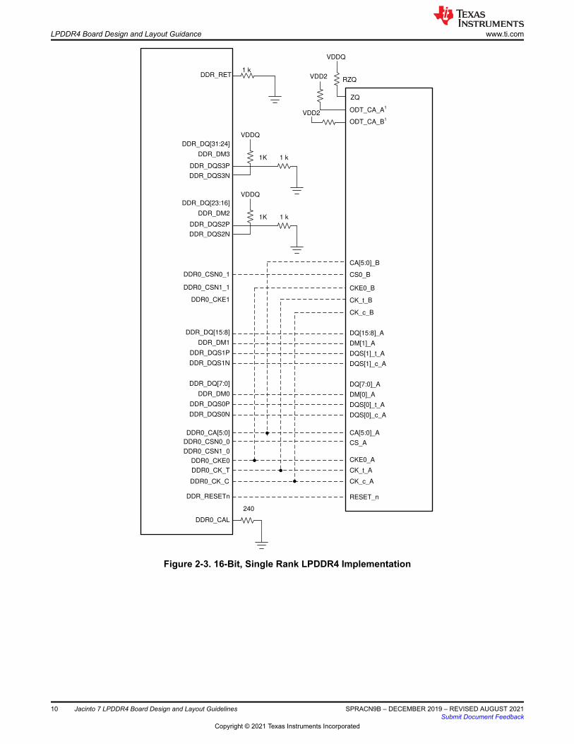
2.3 LPDDR4 Interface SchematicsThe LPDDR4 interface schematics vary, depending upon the number of ranks implemented. General connectivity is straightforward and consistent between the implementations. Figure 2-1 illustrates a 32-bit, single-rank LPDDR4 implementation. If dual rank is required, the additional chip select is included. Figure 2-2 illustrates a 32-bit, dual-rank LPDDR4 implementation. On select devices, 16-bit single-rank LPDDR4 implementation are support, see Figure 2-3.
Note
Though LPDDR4 SDRAMs pin out two separate channels, independent channel use is not supported by this processor.
www.ti.com LPDDR4 Board Design and Layout Guidance
SPRACN9B – DECEMBER 2019 – REVISED AUGUST 2021Submit Document Feedback
Jacinto 7 LPDDR4 Board Design and Layout Guidelines 7
Copyright © 2021 Texas Instruments Incorporated
240
VDD2
VDD2RZQ
VDDQ
1 k
DDR_DQ[31:24]
DDR_DM3
DDR_DQS3P
DDR_DQS3N
DDR_DQ[23:16]
DDR_DM2
DDR_DQS2P
DDR_DQS2N
DDR0_CSN0_1
DDR0_CSN1_1
DDR0_CKE1
DDR_DQ[15:8]
DDR_DM1
DDR_DQS1P
DDR_DQS1N
DDR_DQ[7:0]
DDR_DM0
DDR_DQS0P
DDR_DQS0N
DDR0_CA[5:0]
DDR0_CSN0_0
DDR0_CSN1_0
DDR0_CKE0
DDR0_CK_T
DDR_RESETn
DDR0_CAL
ODT_CA_A1
ODT_CA_B1
DQ[15:8]_B
DM[1]_B
DQS[1]_t_B
DQS[1]_c_B
DQ[7:0]_B
DM[0]_B
DQS[0]_t_B
DQS[0]_c_B
CA[5:0]_B
CS0_B
CKE0_B
CK_t_B
CK_c_B
DQ[15:8]_A
DM[1]_A
DQS[1]_t_A
DQS[1]_c_A
DQ[7:0]_A
DM[0]_A
DQS[0]_t_A
DQS[0]_c_A
CA[5:0]_A
CS_A
CKE0_A
CK_t_A
CK_c_A
RESET_n
ZQ
DDR0_CK_C
DDR_RET
Figure 2-1. 32-Bit, Single-Rank LPDDR4 Implementation
LPDDR4 Board Design and Layout Guidance www.ti.com
8 Jacinto 7 LPDDR4 Board Design and Layout Guidelines SPRACN9B – DECEMBER 2019 – REVISED AUGUST 2021Submit Document Feedback
Copyright © 2021 Texas Instruments Incorporated

240
VDD2
VDD2RZQ
VDDQ
1 k
DDR_DQ[31:24]
DDR_DM3
DDR_DQS3P
DDR_DQS3N
DDR_DQ[23:16]
DDR_DM2
DDR_DQS2P
DDR_DQS2N
DDR0_CSN0_1
DDR0_CSN1_1
DDR0_CKE1
DDR_DQ[15:8]
DDR_DM1
DDR_DQS1P
DDR_DQS1N
DDR_DQ[7:0]
DDR_DM0
DDR_DQS0P
DDR_DQS0N
DDR0_CA[5:0]
DDR0_CSN0_0
DDR0_CSN1_0
DDR0_CKE0
DDR0_CK_T
DDR0_RESETn
DDR0_CAL
ODT_CA_A1
ODT_CA_B1
DQ[15:8]_B
DM[1]_B
DQS[1]_t_B
DQS[1]_c_B
DQ[7:0]_B
DM[0]_B
DQS[0]_t_B
DQS[0]_c_B
CA[5:0]_B
CS0_B
CKE0_B
CKE1_B
CK_c_B
DQ[15:8]_A
DM[1]_A
DQS[1]_t_A
DQS[1]_c_A
DQ[7:0]_A
DM[0]_A
DQS[0]_t_A
DQS[0]_c_A
CA[5:0]_A
CS0_A
CKE0_A
CK_t_A
CK_c_A
RESET_n
ZQ
DDR0_CK_C
DDR_RET
CS1_B
CS1_A
CK_1_B
CKE1_A
Figure 2-2. 32-Bit, Dual Rank LPDDR4 Implementation
www.ti.com LPDDR4 Board Design and Layout Guidance
SPRACN9B – DECEMBER 2019 – REVISED AUGUST 2021Submit Document Feedback
Jacinto 7 LPDDR4 Board Design and Layout Guidelines 9
Copyright © 2021 Texas Instruments Incorporated
240
VDD2
VDD2RZQ
VDDQ
1 k
DDR_DQ[31:24]
DDR_DM3
DDR_DQS3P
DDR_DQS3N
DDR_DQ[23:16]
DDR_DM2
DDR_DQS2P
DDR_DQS2N
DDR0_CSN0_1
DDR0_CSN1_1
DDR0_CKE1
DDR_DQ[15:8]
DDR_DM1
DDR_DQS1P
DDR_DQS1N
DDR_DQ[7:0]
DDR_DM0
DDR_DQS0P
DDR_DQS0N
DDR0_CA[5:0]
DDR0_CSN0_0
DDR0_CSN1_0
DDR0_CKE0
DDR0_CK_T
DDR_RESETn
DDR0_CAL
ODT_CA_A1
ODT_CA_B1
CA[5:0]_B
CS0_B
CKE0_B
CK_t_B
CK_c_B
DQ[15:8]_A
DM[1]_A
DQS[1]_t_A
DQS[1]_c_A
DQ[7:0]_A
DM[0]_A
DQS[0]_t_A
DQS[0]_c_A
CA[5:0]_A
CS_A
CKE0_A
CK_t_A
CK_c_A
RESET_n
ZQ
DDR0_CK_C
DDR_RET
1 k1K
VDDQ
1 k1K
VDDQ
Figure 2-3. 16-Bit, Single Rank LPDDR4 Implementation
LPDDR4 Board Design and Layout Guidance www.ti.com
10 Jacinto 7 LPDDR4 Board Design and Layout Guidelines SPRACN9B – DECEMBER 2019 – REVISED AUGUST 2021Submit Document Feedback
Copyright © 2021 Texas Instruments Incorporated
2.4 Compatible JEDEC LPDDR4 DevicesTable 2-2 shows the parameters of the JEDEC LPDDR4 devices compatible with this interface.
Table 2-2. Compatible JEDEC LPDDR4 DevicesNumber Parameter MIN MAX UNIT
1 Data Rate(1) (2) 4266 MT/s
2 Channel Bit Width x16 x16 Bits
3 Channels 1 2 -
4 Ranks 1 2 -
5 Die 1 4 -
6 Device Count 1 1 -
(1) For supported data rates, see the device-specific data manual.(2) SDRAMs in faster speed grades can be used, provided they are properly configured to operate at the supported data rates. Faster
speed grade SDRAMs may have faster edge rates, which may affect signal integrity. SDRAMs with faster speed grades must be validated on the target board design.
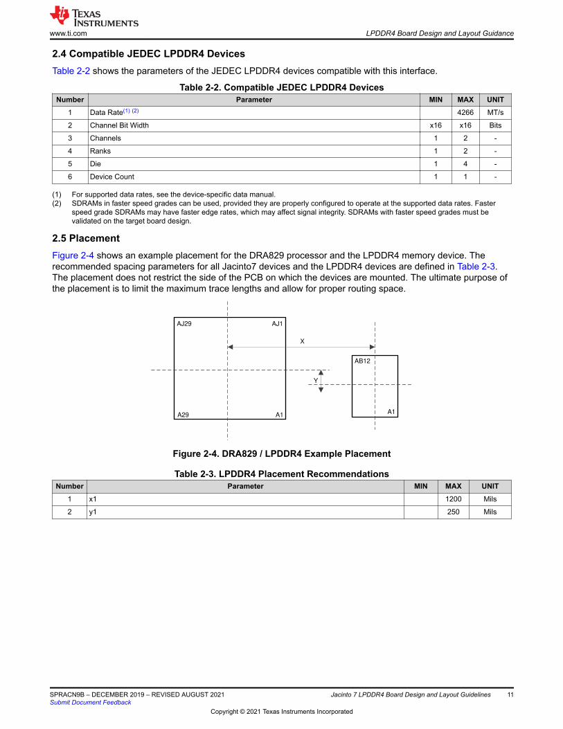
2.5 PlacementFigure 2-4 shows an example placement for the DRA829 processor and the LPDDR4 memory device. The recommended spacing parameters for all Jacinto7 devices and the LPDDR4 devices are defined in Table 2-3. The placement does not restrict the side of the PCB on which the devices are mounted. The ultimate purpose of the placement is to limit the maximum trace lengths and allow for proper routing space.
AJ29 AJ1
A1A29A1
AB12
Y
X
Figure 2-4. DRA829 / LPDDR4 Example Placement
Table 2-3. LPDDR4 Placement RecommendationsNumber Parameter MIN MAX UNIT
1 x1 1200 Mils
2 y1 250 Mils
www.ti.com LPDDR4 Board Design and Layout Guidance
SPRACN9B – DECEMBER 2019 – REVISED AUGUST 2021Submit Document Feedback
Jacinto 7 LPDDR4 Board Design and Layout Guidelines 11
Copyright © 2021 Texas Instruments Incorporated
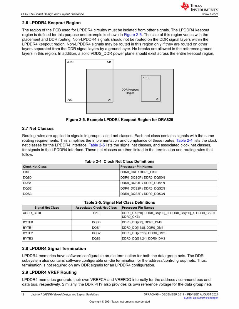
2.6 LPDDR4 Keepout RegionThe region of the PCB used for LPDDR4 circuitry must be isolated from other signals. The LPDDR4 keepout region is defined for this purpose and example is shown in Figure 2-5. The size of this region varies with the placement and DDR routing. Non-LPDDR4 signals should not be routed on the DDR signal layers within the LPDDR4 keepout region. Non-LPDDR4 signals may be routed in this region only if they are routed on other layers separated from the DDR signal layers by a ground layer. No breaks are allowed in the reference ground layers in this region. In addition, a solid VDDS_DDR power plane should exist across the entire keepout region.
AJ29 AJ1
A29
DDR Keepout
Region
A1
AB12
A1
Figure 2-5. Example LPDDR4 Keepout Region for DRA829
2.7 Net ClassesRouting rules are applied to signals in groups called net classes. Each net class contains signals with the same routing requirements. This simplifies the implementation and compliance of these routes. Table 2-4 lists the clock net classes for the LPDDR4 interface. Table 2-5 lists the signal net classes, and associated clock net classes, for signals in the LPDDR4 interface. These net classes are then linked to the termination and routing rules that follow.
Table 2-4. Clock Net Class DefinitionsClock Net Class Processor Pin NamesCK0 DDR0_CKP / DDR0_CKN
DQS0 DDR0_DQS0P / DDR0_DQS0N
DQS1 DDR0_DQS1P / DDR0_DQS1N
DQS2 DDR0_DQS2P / DDR0_DQS2N
DQS3 DDR0_DQS3P / DDR0_DQS3N
Table 2-5. Signal Net Class DefinitionsSignal Net Class Associated Clock Net Class Processor Pin Names
ADDR_CTRL CK0 DDR0_CA[5:0], DDR0_CS[1:0]_0, DDR0_CS[1:0]_1, DDR0_CKE0, DDR0_CKE1
BYTE0 DQS0 DDR0_DQ[7:0], DDR0_DM0
BYTE1 DQS1 DDR0_DQ[15:8], DDR0_DM1
BYTE2 DQS2 DDR0_DQ[23:16], DDR0_DM2
BYTE3 DQS3 DDR0_DQ[31:24], DDR0_DM3
2.8 LPDDR4 Signal TerminationLPDDR4 memories have software configurable on-die termination for both the data group nets. The DDR subsystem also contains software configurable on-die termination for the address/control group nets. Thus, termination is not required on any DDR signals for an LPDDR4 configuration.
2.9 LPDDR4 VREF RoutingLPDDR4 memories generate their own VREFCA and VREFDQ internally for the address / command bus and data bus, respectively. Similarly, the DDR PHY also provides its own reference voltage for the data group nets
LPDDR4 Board Design and Layout Guidance www.ti.com
12 Jacinto 7 LPDDR4 Board Design and Layout Guidelines SPRACN9B – DECEMBER 2019 – REVISED AUGUST 2021Submit Document Feedback
Copyright © 2021 Texas Instruments Incorporated
during reads. Thus unlike DDR3 and DDR4, VREF does not need to be generated on the board, and there is no required VREF routing for an LPDDR4 configuration.
2.10 LPDDR4 VTTUnlike DDR3 and DDR4, there is no required termination on the PCB of the address/control bus of an LPDDR4 configuration. All termination is handled internally (on-die). Thus, VTT does not apply for LPDDR4.
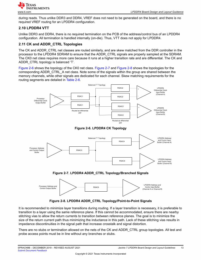
2.11 CK and ADDR_CTRL TopologiesThe CK and ADDR_CTRL net classes are routed similarly, and are skew matched from the DDR controller in the processor to the LPDDR4 SDRAM to ensure that the ADDR_CTRL signals are properly sampled at the SDRAM. The CK0 net class requires more care because it runs at a higher transition rate and are differential. The CK and ADDR_CTRL topology is balanced ‘T’.
Figure 2-6 shows the topology of the CK0 net class. Figure 2-7 and Figure 2-8 shows the topologies for the corresponding ADDR_CTRL_A net class. Note some of the signals within the group are shared between the memory channels, while other signals are dedicated for each channel. Skew matching requirements for the routing segments are detailed in Table 2-6.
RSAC1
RSAC1
+
-
+
-
RSAC2
RSAC2
+
-
RSAC2
RSAC2
LPDDR4
Differential Clock
Input Buffer
(Channel A)
LPDDR4
Differential Clock
Input Buffer
(Channel B)
Processor Differential Clock
Output Buffer
Routed as differential
pair
Routed as differential
pair
%DODQFHGµ7¶7RSRORJ\
Figure 2-6. LPDDR4 CK Topology
RSAC3
RSAC4
RSAC4
LPDDR4 Address
and Contro Input
Buffer (Channel A)
LPDDR4 Address
and Contro Input
Buffer (Channel B)
Processor Address
and Control Output
Buffer
%DODQFHGµ7¶7RSRORJ\
Figure 2-7. LPDDR4 ADDR_CTRL Topology/Branched Signals
RSAC5
LPDDR4 Address and
Contro Input Buffer
(Channel A or Channel B)
Processor Address and
Control Output Buffer
Figure 2-8. LPDDR4 ADDR_CTRL Topology/Point-to-Point Signals
It is recommended to minimize layer transitions during routing. If a layer transition is necessary, it is preferable to transition to a layer using the same reference plane. If this cannot be accommodated, ensure there are nearby stitching vias to allow the return currents to transition between reference planes. The goal is to minimize the size of the return current path thus minimizing the inductance in this path. Lack of these stitching vias results in impedance discontinuities in the signal path that increase crosstalk and signal distortion.
There are no stubs or termination allowed on the nets of the CK and ADDR_CTRL group topologies. All test and probe access points must be in line without any branches or stubs.
www.ti.com LPDDR4 Board Design and Layout Guidance
SPRACN9B – DECEMBER 2019 – REVISED AUGUST 2021Submit Document Feedback
Jacinto 7 LPDDR4 Board Design and Layout Guidelines 13
Copyright © 2021 Texas Instruments Incorporated

2.12 Data Group TopologiesThe data line topology is always point-to-point for LPDDR4 implementations, and is broken up into four different byte lanes. It is recommended to minimize layer transitions during routing. If a layer transition is necessary, it is better to transition to a layer using the same reference plane. If this cannot be accommodated, ensure there are nearby ground vias to allow the return currents to transition between reference planes. The goal is to provide a low inductance path for the return current. To optimize the skew matching, TI recommends routing all nets within a single data routing group on one layer where all nets have the exact same number of vias and the same via barrel length.
DQSP and DQSN lines are point-to-point signals routed as a differential pair. Figure 2-9 illustrates the DQSP/N connection topology.
Processor
DQS IO
Buffer
DDR
SDRAM
DQS IO
Buffer
RSD1
RSD1
Routed as differential pair
+
±
+
±
Figure 2-9. LPDDR4 DQS Topology
DQ and DM lines are point-to-point signals routed as single-ended. Figure 2-10 illustrates the DQ and DM connection topology.
RSD2
DDR
SDRAM
DQ and DM
IO Buffer
Processor
DQ and DM
IO Buffer
Figure 2-10. LPDDR4 DQ/DM Topology
There are no stubs or termination allowed on the nets of the data group topologies. All test and probe access points must be in line without any branches or stubs.
LPDDR4 Board Design and Layout Guidance www.ti.com
14 Jacinto 7 LPDDR4 Board Design and Layout Guidelines SPRACN9B – DECEMBER 2019 – REVISED AUGUST 2021Submit Document Feedback
Copyright © 2021 Texas Instruments Incorporated
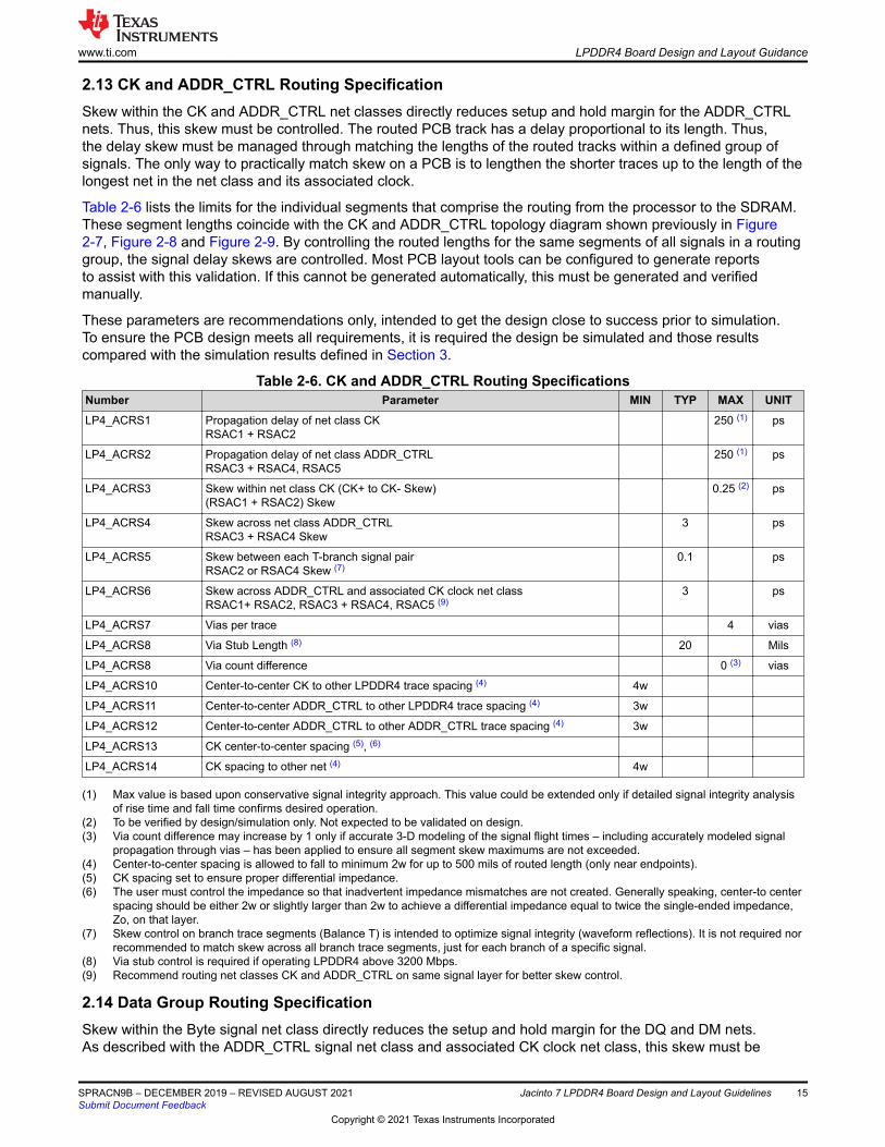
2.13 CK and ADDR_CTRL Routing SpecificationSkew within the CK and ADDR_CTRL net classes directly reduces setup and hold margin for the ADDR_CTRL nets. Thus, this skew must be controlled. The routed PCB track has a delay proportional to its length. Thus, the delay skew must be managed through matching the lengths of the routed tracks within a defined group of signals. The only way to practically match skew on a PCB is to lengthen the shorter traces up to the length of the longest net in the net class and its associated clock.
Table 2-6 lists the limits for the individual segments that comprise the routing from the processor to the SDRAM. These segment lengths coincide with the CK and ADDR_CTRL topology diagram shown previously in Figure 2-7, Figure 2-8 and Figure 2-9. By controlling the routed lengths for the same segments of all signals in a routing group, the signal delay skews are controlled. Most PCB layout tools can be configured to generate reports to assist with this validation. If this cannot be generated automatically, this must be generated and verified manually.
These parameters are recommendations only, intended to get the design close to success prior to simulation. To ensure the PCB design meets all requirements, it is required the design be simulated and those results compared with the simulation results defined in Section 3.
Table 2-6. CK and ADDR_CTRL Routing SpecificationsNumber Parameter MIN TYP MAX UNITLP4_ACRS1 Propagation delay of net class CK
RSAC1 + RSAC2250 (1) ps
LP4_ACRS2 Propagation delay of net class ADDR_CTRLRSAC3 + RSAC4, RSAC5
250 (1) ps
LP4_ACRS3 Skew within net class CK (CK+ to CK- Skew)(RSAC1 + RSAC2) Skew
0.25 (2) ps
LP4_ACRS4 Skew across net class ADDR_CTRLRSAC3 + RSAC4 Skew
3 ps
LP4_ACRS5 Skew between each T-branch signal pairRSAC2 or RSAC4 Skew (7)
0.1 ps
LP4_ACRS6 Skew across ADDR_CTRL and associated CK clock net classRSAC1+ RSAC2, RSAC3 + RSAC4, RSAC5 (9)
3 ps
LP4_ACRS7 Vias per trace 4 vias
LP4_ACRS8 Via Stub Length (8) 20 Mils
LP4_ACRS8 Via count difference 0 (3) vias
LP4_ACRS10 Center-to-center CK to other LPDDR4 trace spacing (4) 4w
LP4_ACRS11 Center-to-center ADDR_CTRL to other LPDDR4 trace spacing (4) 3w
LP4_ACRS12 Center-to-center ADDR_CTRL to other ADDR_CTRL trace spacing (4) 3w
LP4_ACRS13 CK center-to-center spacing (5), (6)
LP4_ACRS14 CK spacing to other net (4) 4w
(1) Max value is based upon conservative signal integrity approach. This value could be extended only if detailed signal integrity analysis of rise time and fall time confirms desired operation.
(2) To be verified by design/simulation only. Not expected to be validated on design.(3) Via count difference may increase by 1 only if accurate 3-D modeling of the signal flight times – including accurately modeled signal
propagation through vias – has been applied to ensure all segment skew maximums are not exceeded.(4) Center-to-center spacing is allowed to fall to minimum 2w for up to 500 mils of routed length (only near endpoints).(5) CK spacing set to ensure proper differential impedance.(6) The user must control the impedance so that inadvertent impedance mismatches are not created. Generally speaking, center-to center
spacing should be either 2w or slightly larger than 2w to achieve a differential impedance equal to twice the single-ended impedance, Zo, on that layer.
(7) Skew control on branch trace segments (Balance T) is intended to optimize signal integrity (waveform reflections). It is not required nor recommended to match skew across all branch trace segments, just for each branch of a specific signal.
(8) Via stub control is required if operating LPDDR4 above 3200 Mbps.(9) Recommend routing net classes CK and ADDR_CTRL on same signal layer for better skew control.
2.14 Data Group Routing SpecificationSkew within the Byte signal net class directly reduces the setup and hold margin for the DQ and DM nets. As described with the ADDR_CTRL signal net class and associated CK clock net class, this skew must be
www.ti.com LPDDR4 Board Design and Layout Guidance
SPRACN9B – DECEMBER 2019 – REVISED AUGUST 2021Submit Document Feedback
Jacinto 7 LPDDR4 Board Design and Layout Guidelines 15
Copyright © 2021 Texas Instruments Incorporated

controlled. The data byte skew must be managed through controlling the lengths of the routed tracks within a defined group of signals. The only way to practically match skews on a PCB is to lengthen the shorter traces up to the length of the longest net in the net class and its associated clock.
Note
It is not required nor recommended to match the lengths across all byte lanes. Length matching is only required within each byte.
Table 2-7 contains the routing specifications for the Byte0, Byte1, Byte2, and Byte3 routing groups. Each signal net class and its associated clock net class is routed and matched independently. These parameters are recommendations only, intended to get the design close to success prior to simulation. To ensure the PCB design meets all requirements, it is required the design be simulated and those results compared with the simulation results defined in Section 3.
Table 2-7. Data Group Routing SpecificationsNumber Parameter MIN TYP MAX UNITLP4_DRS1 Propagation delay of net class DQSx
RSD1 (5)250 (3) ps
LP4_DRS2 Propagation delay of net class BYTExRSD2
250 (3) ps
LP4_DRS3 Propagation delay of each DQS pair must be less than propagation delay of CK pair. RSD1 < (RSAC1 + RSAC2) (5)
0 ps
LP4_DRS4 Skew within net class DQSxRSD1 Skew (DQS+ to DQS-) (6)
0.1 ps
LP4_DRS5 Skew across net class DQSx and BYTExRSD1 to RSD2 Skew (1), (2), (6)
0.5 ps
LP4_DRS6 Propagation delay of each DQS pair must be less than propagation delay DQ/DM. RSD1 < RSD2 (5)
0 ps
LP4_DRS7 Vias Per Trace 2 (3) vias
LP4_DRS8 Via Stub Length (4) 40 Mils
LP4_DRS9 Via Count Difference 0 (7) vias
LP4_DRS10 RSD1 center-to-center spacing (between clock net class) (8) 4w
LP4_DRS11 RSD1 center-to-center spacing (within clock net class) (9), (10)
LP4_DRS12 RSD2 center-to-center spacing (between signal net class) (8) 4w
LP4_DRS13 RSD2 center-to-center spacing (within signal net class)(5) 3w
(1) Skew matching is only done within a byte. Skew matching across bytes is neither required nor recommended.(2) Each DQS pair is length matched to its associated byte.(3) Max value is based upon conservative signal integrity approach. This value could be extended only if detailed signal integrity analysis
of rise time and fall time confirms desired operation.(4) Via stub control is required if operating LPDDR4 above 3200 Mbps.(5) This is a system level requirement, and must include memory package in computation.(6) To be verified by design/simulation only. Not expected to be validated on design.(7) Via count difference may increase by 1 only if accurate 3-D modeling of the signal flight times – including accurately modeled signal
propagation through vias – has been applied to ensure DQn skew and DQSn to DQn skew maximums are not exceeded.(8) Center-to-center spacing is allowed to fall to minimum 2w for up to 500 mils of routed length (only near endpoints).(9) DQS pair spacing is set to ensure proper differential impedance.(10) The Simulation Results must control the impedance so that inadvertent impedance mismatches are not created. Generally speaking,
center-to center spacing should be either 2w or slightly larger than 2w to achieve a differential impedance equal to twice the single-ended impedance, Zo, on that layer.
2.15 Channel, Byte, and Bit SwappingAll signals, including data and address/control, must be routed 1 to 1 from the DDR controller to the LPDDR4 memory. Byte swapping across channels or within a channel is not allowed. Similarly, data bit swapping across byte lanes or within a byte is also not allowed. In addition, byte lanes 0 and 1 of the DDR controller must be routed to channel A of the LPDDR4 memory, and byte lanes 2 and 3 of the DDR controller must be routed to channel B of the LPDDR4 memory.
LPDDR4 Board Design and Layout Guidance www.ti.com
16 Jacinto 7 LPDDR4 Board Design and Layout Guidelines SPRACN9B – DECEMBER 2019 – REVISED AUGUST 2021Submit Document Feedback
Copyright © 2021 Texas Instruments Incorporated
3 LPDDR4 Board Design SimulationsThis section is intended to provide an overview of the basic system-level board extraction, simulation, and analysis methodologies for high-speed LPDDR4 interfaces. This is an essential step to ensure the PCB design meets all the requirements to operate the targeted speeds.
3.1 Board Model ExtractionThe board level extraction guidelines listed below are intended to work in any EDA extraction tool and are not tool-specific. It is important to follow the steps outlined in Section 3.2 through Section 3.4 immediately after completing touchstone model extractions. The design should be checked with these steps prior to running IBIS simulations.
1. For DDR extractions, extract power (VDDS_DDR/VDDQ and VDDS_DDR_BIAS/VDDQX) and signal nets together in a 3D-EM solver. For SerDes extractions power is not required as the simulations are only intended for Signal Integrity
2. Use wide-band models. It is recommended to extract from DC to at least till 6x the Nyquist frequency (for example, for LPDDR4-4266 extract the model at least till 12.8 GHz).
3. Check the board stack-up for accurate layer thickness and material properties.a. It is recommended to use Djordjevic-Sarkar models for the dielectric material definition.
4. Use accurate etch profiles and surface roughness for the signal traces across all layers in the stack-up.5. If the board layout is cut prior to extraction (to reduce simulation time), please define a cut boundary that is
at least 0.25 inch away from the signal and power nets.6. Check the via padstack definitions.
a. Ensure that the non-functional internal layer pads on signal vias are modeled the same way they would be fabricated.
b. These non-functional internal layer pads on signal vias are not recommended by TI.7. Use Spice/S-parameter models (typically available from the vendor) for modeling all passives in the system
3.2 Board-Model ValidationThe extracted board models need to be checked for the following properties:
• Passivity: This ensures that the board model is a passive network and does not generate energy• Causality: This ensures that the board model obeys the causal relationship i.e. output follows input.
These checks can be performed in any standard EDA simulator or extraction engine.
3.3 S-Parameter InspectionOnce the extracted S-parameters have been verified as causal and passive, the S-parameter plots should be inspected. It is recommended to check for the following:
• Insertion Loss: The single-ended insertion loss is recommended to stay within 0 to 10 dB up to 3 times the Nyquist frequency of operation. For example, if the target frequency is 8 Gbps (4GHz Nyquist), the single-ended insertion loss should stay under 10 dB up to 12 GHz.
• Return Loss: The single-ended return loss is recommended to be less than 15 dB up to 3 times the Nyquist frequency.
• Near and Far end crosstalk (FEXT/NEXT): The FEXT and NEXT are recommended to be under 25 dB for frequencies up to 3 times the Nyquist frequency.
The S-Parameter inspection plots are not pass/fail tests, but rather its more of a guide to check if the design has a reasonable chance of performing a the required level.
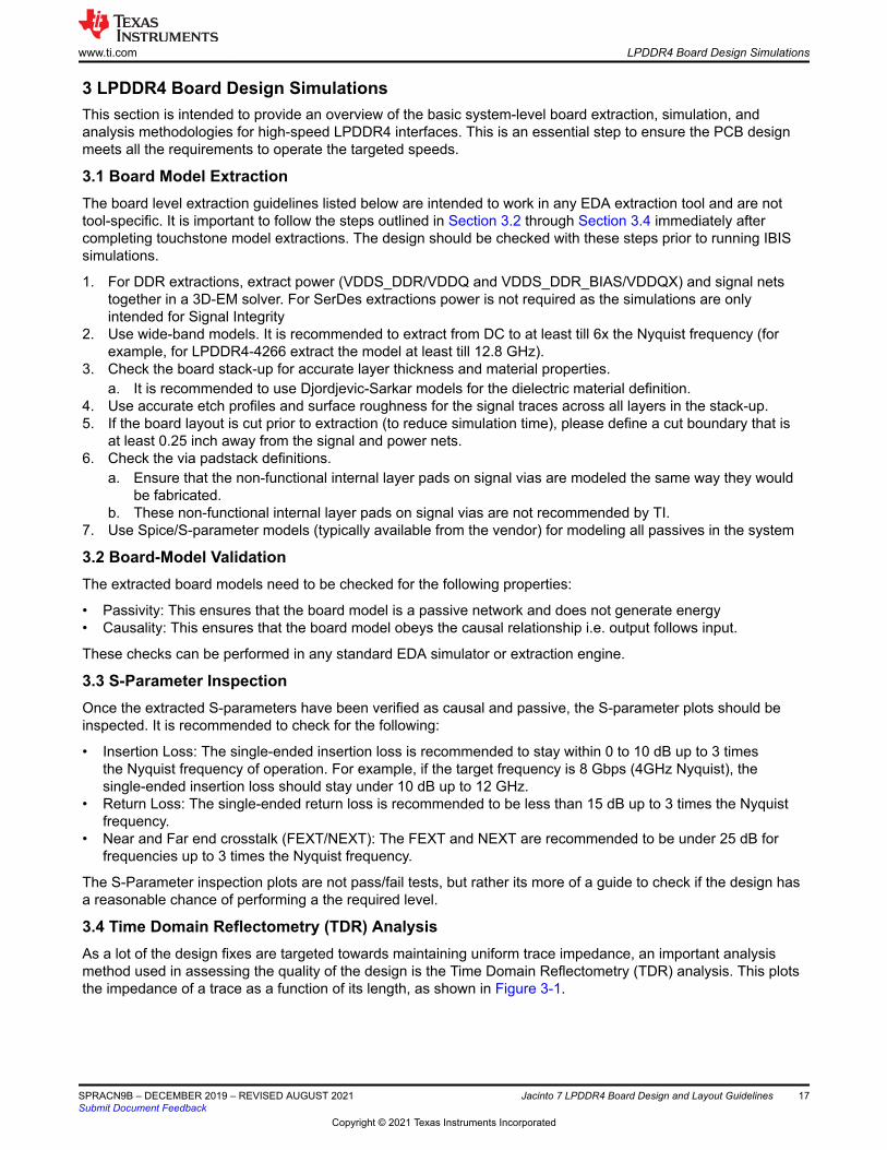
3.4 Time Domain Reflectometry (TDR) AnalysisAs a lot of the design fixes are targeted towards maintaining uniform trace impedance, an important analysis method used in assessing the quality of the design is the Time Domain Reflectometry (TDR) analysis. This plots the impedance of a trace as a function of its length, as shown in Figure 3-1.
www.ti.com LPDDR4 Board Design Simulations
SPRACN9B – DECEMBER 2019 – REVISED AUGUST 2021Submit Document Feedback
Jacinto 7 LPDDR4 Board Design and Layout Guidelines 17
Copyright © 2021 Texas Instruments Incorporated
Figure 3-1. TDR Plot Example With Impedance Mismatch
As shown in Figure 3-1, the TDR plot highlights impedance discontinuities in the trace from one end to the other. This method depends on a reflected waveform from the far-end of the trace. The delay in the plot corresponding to a particular point in the trace actually corresponds to 2 times the distance of that point from the source, owing to the round trip time. This needs to be factored in for assessing the source of impedance discontinuities.
The TDR plot can be generated by reading in the S-parameter models generated by the extraction tool and assessing them in “Time-Domain” mode. A standard EDA simulator such as HyperLynx can perform this function. It is recommended to optimize the design to within a ± 5% deviation from the nominal trace impedance.
The TDR plots are not pass/fail tests, but rather is more of a guide to check if the design has a reasonable chance of performing a the required level.
LPDDR4 Board Design Simulations www.ti.com
18 Jacinto 7 LPDDR4 Board Design and Layout Guidelines SPRACN9B – DECEMBER 2019 – REVISED AUGUST 2021Submit Document Feedback
Copyright © 2021 Texas Instruments Incorporated

3.5 Simulation Integrity AnalysisThe methodology for validating the DDR interface is outlined in this section. LPDDR4 interfaces, as defined in the JEDEC specification, uses eye masks defined at a target BER (Bit Error Rate) to determine pass or fail for signal integrity. It is essential to perform channel simulations using IBIS models to generate the signal eye diagrams at the targeted BER. Channel simulation techniques are widely used in SerDes interface analysis. These are introduced for memory interfaces starting from DDR4 and LPDDR4
3.5.1 Simulation Setup
Set up the system-level schematic in the simulator by connecting the SOC IBIS model, board model, power supplies, DRAM package model, and DRAM IBIS model. A typical system-level DDR schematic is shown in Figure 3-2.
Note
Be aware of the DRAM configuration (number of dies in the package, number of ranks, and number of channels) while setting up the system schematic.
Be aware the DRAM configuration may also include On-Die Decoupling Circuit.
Figure 3-2. Typical System-Level DDR Schematic
• LPDDR4 simulations require power-aware IBIS models for the controller and the memory along with a simulator that supports channel simulations for DDR interfaces.
• SPICE-based transistor-level simulations cannot be used for generating BER signal eyes. Use a simulator that can handle power-aware IBIS simulations and can run channel simulations for the DDR interface.
• IBIS models reduce simulation time with minimal loss in accuracy compared with SPICE-based transistor-level simulations. IBIS models starting from version 5.0 are power-aware models which enables Simultaneous Switching Output (SSO) noise simulations. The TI IBIS model is a power-aware IBIS model.
• Use SPICE models to accurately model the on-die decoupling capacitance on the DDR supply net for both – controller and DRAM. This ensures accurate power noise and Power Supply Induced Jitter (PSIJ) estimation in DDR simulations. The on-die decoupling capacitance information for the DRAM can be obtained from the DRAM vendor.
• Use SPICE or S-parameter files to model the DRAM package. This can be requested from the DRAM vendor. EBD models are not recommended.
www.ti.com LPDDR4 Board Design Simulations
SPRACN9B – DECEMBER 2019 – REVISED AUGUST 2021Submit Document Feedback
Jacinto 7 LPDDR4 Board Design and Layout Guidelines 19
Copyright © 2021 Texas Instruments Incorporated
• J7ES model for the on-die decoupling capacitance on the DDR supply net:******************************************* On-die Decoupling circuit for J7ES (DIE_VDDS_DDR to VSS)******************************************* Notes:* Includes on-die decoupling for all DDR signals ** This subcircuit should be added across the J7ES IBIS model's* DIE_VDDS_DDR and VSS pins******************************************** x_decouple DIE_VDDS_DDR vss_die J7ES_ondie_decoupling_alldq******************************************.SUBCKTJ7ES_ondie_decoupling_alldq DIE_VDDS_DDR vss_dieCvddq_c DIE_VDDS_DDR DIE_VDDS_DDR_c 2105.86e-12Rvddq_c vss_die DIE_VDDS_DDR_c 43e-3.ENDS
3.5.2 Simulation Parameters
It is important to configure the simulation to exercise the system to real, but worst case parameters.
• Use the worst-case bit pattern to excite the system. The simulator should be able to generate the worst-case bit pattern based on channel characterization.
• Select the controller and DRAM models (sets the drive strength, ODT, VOH levels, and so forth) from the IBIS files which work best for the system.– This is typically an iterative process.– Every system is unique and the optimal settings for these parameters can vary from system to system.
Table 3-1. Example Data Write ODI/ODT Optimization
Pkg Byte Board ODI Ω ODT ΩTotal EW
Margin (ps)
Total EH Margin (mV)B
B3 J7 370HR 10L Ref B3, No BD 40 40 50.28 15.66
B3 J7 370HR 10L Ref B3, No BD 40 48 27.62 11.76
B3 J7 370HR 10L Ref B3, No BD 40 40 33.52 2.92
B3 J7 370HR 10L Ref B3, No BD 48 48 1.54 0.86
• Data bus and address bus ODT and drive strength values can be set independently. As an example, the J721E EVM used 40-Ω ODT for data read/writes and 80-Ω for CA bus. Drive strength of 40-ohms for data read/write and CA.– Data READ Controller model - lpddr4_odt_40, lpddr4_odt_40_diff– Data WRITE Controller model - lpddr4_ocd_40p_40n, lpddr4_ocd_40p_40n_diff– CA/CLK Controller model - lpddr4_ocd_40p_40n, lpddr4_ocd_40p_40n_diff
• Set up the channel simulation parameters. These typically consists of the data rate, ignore time/bits, minimum number of bits, bit sampling rate, BER floor, number of bits for display, types of BER eyes (voltage and/or timing), and target BER.– To determine the minimum number of bits one can run a series of channel simulations with different
number of bits. The BER signal eye (and margins) tend to converge after a certain minimum number of bits. This should help determining the minimum number of bits to be used for the system.
– Run channel simulations to generate the eye diagrams at LBER of -16.• Run channel simulations with non-ideal power settings at different PVT corners. It is recommended to run the
simulations at least at the SSHT and FFLT corners.
3.5.3 Simulation Targets
Once the simulation successfully completes, generate the DDR analysis reports from the simulation tool. There are several different parameters to be verified, detailed in this section. Each parameter is pass/fail, meaning each must meet the specified target to ensure the design has sufficient margin to operate at the target data rates.
LPDDR4 Board Design Simulations www.ti.com
20 Jacinto 7 LPDDR4 Board Design and Layout Guidelines SPRACN9B – DECEMBER 2019 – REVISED AUGUST 2021Submit Document Feedback
Copyright © 2021 Texas Instruments Incorporated
Use the appropriate JEDEC Vref parameters (Vref_min, Vref_max, Vref_step, and Vref_set_tol) and mask parameters (share, height, width).
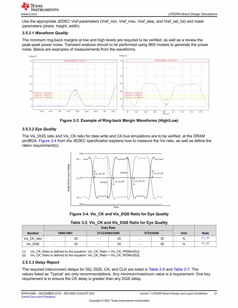
3.5.3.1 Waveform Quality
The minimum ring-back margins at low and high levels are required to be verified, as well as a review the peak-peak power noise. Transient analysis should to be performed using IBIS models to generate the power noise. Below are examples of measurements from the waveforms.
Figure 3-3. Example of Ring-back Margin Waveforms (High/Low)
3.5.3.2 Eye Quality
The Vix_DQS ratio and Vix_CK ratio for data write and CA bus simulations are to be verified, at the DRAM pin/BGA. Figure 3-4 from the JEDEC specification explains how to measure the Vix ratio, as well as define the ration requirement(s).
Figure 3-4. Vix_CK and Vix_DQS Ratio for Eye Quality
Table 3-2. Vix_CK and Vix_DQS Ratio for Eye Quality
SymbolData Rate
Unit Note1600/1867 2133/2400/3200 3733/4266Vix_CK_ratio - 25 - 25 - 25 % (1), (2)
Vix_DQS - 20 - 20 - 20 % (1), (2)
(1) Vix_CK_Ratio is defined by the equation: Vix_CK_Ratio = Vix_CK_FR|Min(f(t))|(2) Vix_CK_Ratio is defined by the equation: Vix_CK_Ratio = Vix_CK_RF|Min(f(t))|
3.5.3.3 Delay Report
The required interconnect delays for DQ, DQS, CA, and CLK are listed in Table 2-6 and Table 2-7. The values listed as ‘Typical’ are only recommendations. Any minimum/maximum value is a requirement. One key requirement is to ensure the CK delay is greater than any DQS delay.
www.ti.com LPDDR4 Board Design Simulations
SPRACN9B – DECEMBER 2019 – REVISED AUGUST 2021Submit Document Feedback
Jacinto 7 LPDDR4 Board Design and Layout Guidelines 21
Copyright © 2021 Texas Instruments Incorporated

3.5.3.4 Mask Report
The minimum jitter and noise margins are to be captured with respect to the eye mask(s). This masks are data rate dependent, and includes:
• Data read eye mask at the SOC die pad for functionality testing• Data write eye mask (JEDEC spec) at the DRAM pin/BGA for compliance testing• CA bus eye mask (JEDEC spec) at the DRAM pin/BGA for compliance testing
There should be at least 2 sets of eye diagrams generated by the simulator:
• Vref set to the optimal Vref of the byte offset by the Vref_set_tol in the positive direction (Vref_set_tol is defined in JEDEC spec)
• Vref set to the optimal Vref of the byte offset by the Vref_set_tol in the negative direction
The system-level margins are the worst case noise and jitter margins from all eye diagram measurements listed above (across SSHT and FFLT corners). For all waveforms captured at the DRAM device, margins should be calculated at both the BGA pin and the DRAM pad.
Table 3-3. LPDDR4/4x Eye Mask Definitions/RequirementsParameter Mask Shape LPDDR4-3200 LPDDR4-3733 LPDDR4-4266CA eye mask TclVW Rectangular (1) 0.3 UI (1) (2) 0.3 UI (1)
CA eye mask VclVW Rectangular (1) 155 mV (1) (2) 145 mV (1)
Write eye mask TdlVW Rectangular (1) 0.25 UI (1) (2) 0.25 UI (1)
Write eye mask VdlVW Rectangular (1) 140 mV (1) (2) 120 mV (1)
Read eye mask TdlVW Diamond 0.61 UI 0.66 UI 0.7 UI
Read eye mask VdlVW Diamond 140 mV 120 mV 120 mV
(1) Copied from JEDEC specification: Low Power Double Date Rate 4 (LPDDR4).(2) For details, contact the DRAM vendor.
LPDDR4 Board Design Simulations www.ti.com
22 Jacinto 7 LPDDR4 Board Design and Layout Guidelines SPRACN9B – DECEMBER 2019 – REVISED AUGUST 2021Submit Document Feedback
Copyright © 2021 Texas Instruments Incorporated

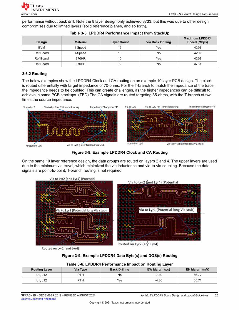
Figure 3-5 through Figure 3-7 show the eye mask definitions translated to eye diagrams within captured waveforms.
Figure 3-5. Sample Simulated LPDDR4-4266 Read Eye With Diamond-Shaped Eye Mask
Figure 3-6. Sample Simulated LPDDR4-4266 Write Eye With Rectangular JEDEC Eye Mask
www.ti.com LPDDR4 Board Design Simulations
SPRACN9B – DECEMBER 2019 – REVISED AUGUST 2021Submit Document Feedback
Jacinto 7 LPDDR4 Board Design and Layout Guidelines 23
Copyright © 2021 Texas Instruments Incorporated
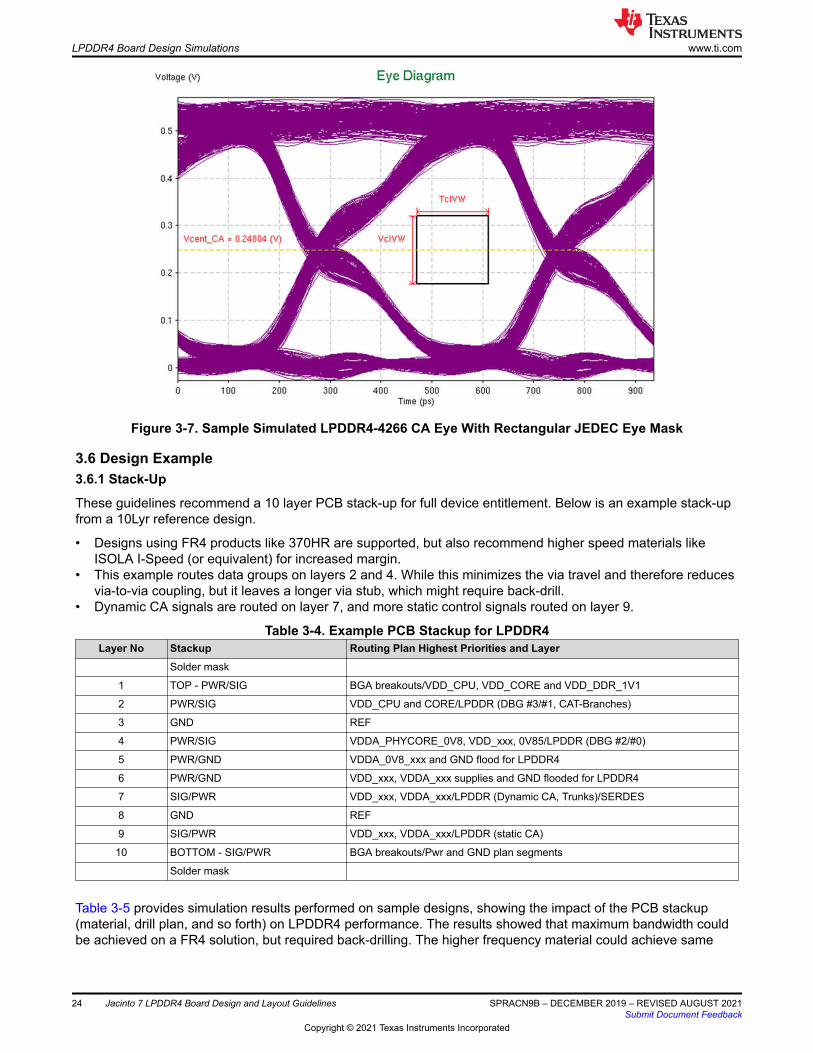
Figure 3-7. Sample Simulated LPDDR4-4266 CA Eye With Rectangular JEDEC Eye Mask
3.6 Design Example3.6.1 Stack-Up
These guidelines recommend a 10 layer PCB stack-up for full device entitlement. Below is an example stack-up from a 10Lyr reference design.
• Designs using FR4 products like 370HR are supported, but also recommend higher speed materials like ISOLA I-Speed (or equivalent) for increased margin.
• This example routes data groups on layers 2 and 4. While this minimizes the via travel and therefore reduces via-to-via coupling, but it leaves a longer via stub, which might require back-drill.
• Dynamic CA signals are routed on layer 7, and more static control signals routed on layer 9.
Table 3-4. Example PCB Stackup for LPDDR4Layer No Stackup Routing Plan Highest Priorities and Layer
Solder mask
1 TOP - PWR/SIG BGA breakouts/VDD_CPU, VDD_CORE and VDD_DDR_1V1
2 PWR/SIG VDD_CPU and CORE/LPDDR (DBG #3/#1, CAT-Branches)
3 GND REF
4 PWR/SIG VDDA_PHYCORE_0V8, VDD_xxx, 0V85/LPDDR (DBG #2/#0)
5 PWR/GND VDDA_0V8_xxx and GND flood for LPDDR4
6 PWR/GND VDD_xxx, VDDA_xxx supplies and GND flooded for LPDDR4
7 SIG/PWR VDD_xxx, VDDA_xxx/LPDDR (Dynamic CA, Trunks)/SERDES
8 GND REF
9 SIG/PWR VDD_xxx, VDDA_xxx/LPDDR (static CA)
10 BOTTOM - SIG/PWR BGA breakouts/Pwr and GND plan segments
Solder mask
Table 3-5 provides simulation results performed on sample designs, showing the impact of the PCB stackup (material, drill plan, and so forth) on LPDDR4 performance. The results showed that maximum bandwidth could be achieved on a FR4 solution, but required back-drilling. The higher frequency material could achieve same
LPDDR4 Board Design Simulations www.ti.com
24 Jacinto 7 LPDDR4 Board Design and Layout Guidelines SPRACN9B – DECEMBER 2019 – REVISED AUGUST 2021Submit Document Feedback
Copyright © 2021 Texas Instruments Incorporated
performance without back drill. Note the 8 layer design only achieved 3733, but this was due to other design compromises due to limited layers (solid reference planes, and so forth).
Table 3-5. LPDDR4 Performance Impact from StackUp
Design Material Layer Count Via Back DrillingMaximum LPDDR4
Speed (Mbps)EVM I-Speed 16 Yes 4266
Ref Board I-Speed 10 No 4266
Ref Board 370HR 10 Yes 4266
Ref Board 370HR 8 No 3733
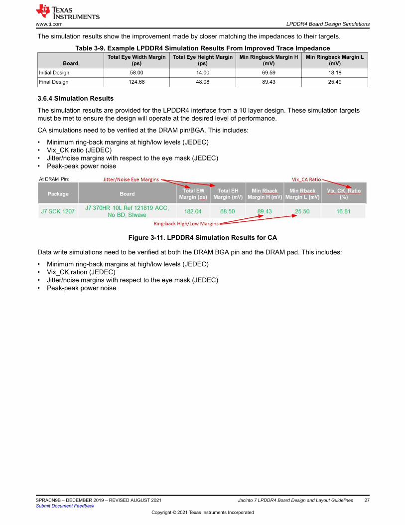
3.6.2 Routing
The below examples show the LPDDR4 Clock and CA routing on an example 10 layer PCB design. The clock is routed differentially with target impedance of 70-ohms. For the T-branch to match the impedance of the trace, the impedance needs to be doubled. This can create challenges, as the higher impedances can be difficult to achieve in some PCB stackups. (TBD) The CA signals are routed targeting 35-ohms, with the T-branch at two times the source impedance.
Figure 3-8. Example LPDDR4 Clock and CA Routing
On the same 10 layer reference design, the data groups are routed on layers 2 and 4. The upper layers are used due to the minimum via travel, which minimized the via inductance and via-to-via coupling. Because the data signals are point-to-point, T-branch routing is not required.
Figure 3-9. Example LPDDR4 Data Byte(s) and DQS(s) Routing
Table 3-6. LPDDR4 Performance Impact on Routing LayerRouting Layer Via Type Back Drilling EW Margin (ps) EH Margin (mV)
L1, L12 PTH No -7.10 56.72
L1, L12 PTH Yes -4.86 55.71
www.ti.com LPDDR4 Board Design Simulations
SPRACN9B – DECEMBER 2019 – REVISED AUGUST 2021Submit Document Feedback
Jacinto 7 LPDDR4 Board Design and Layout Guidelines 25
Copyright © 2021 Texas Instruments Incorporated

Table 3-6. LPDDR4 Performance Impact on Routing Layer (continued)Routing Layer Via Type Back Drilling EW Margin (ps) EH Margin (mV)
L1, L3 PTH No 5.70 40.29
L1, L3 PTH Yes 8.37 34.54
L1, L12 PTH No 17.42 39.22
L1, L12 PTH Yes 20.04 41.93
L1, L3 PTH No 27.66 41.37
L1, L3 PTH Yes 27.76 48.63
3.6.3 Model Verification
Before simulating, it is recommended to verify the models. One verification method described is the impedance plot (or impedance scan). The Impedance scans for a 10 layer design are provided.
Figure 3-10. Example LPDDR4 Trace Impedance Scan
Table 3-7. Example LPDDR4 Trace Impedance Summary for Data
Layer DDR Bus DQ SE Impedance (Ω)DQS/CLK Difference
Impedance (Ω)L2 B1 and B3 40.9 77.7
L2 CA 51.7 101.4
L4 B0 and B2 41.1 77.7
L7 CA 41.1 77.7
For CK and CA signals, the goal is to have the branch segment equal to two times the impedance of the feed trace. Note its common for the PCB to limit the achievable impedances. Simulations will show you if the compromises are acceptable.
Table 3-8. Example LPDDR4 Trace Impedance Summary for CA
Board CA Feed Impedance (Ω)CA Branch Impedance
(Ω) CA Branch Target (Ω) Impedance Mismatch (Ω)Initial Design 49.1 59.6 98 (49x2) 38.6
Final Design 41.1 51.7 82 (41x2) 30.5
LPDDR4 Board Design Simulations www.ti.com
26 Jacinto 7 LPDDR4 Board Design and Layout Guidelines SPRACN9B – DECEMBER 2019 – REVISED AUGUST 2021Submit Document Feedback
Copyright © 2021 Texas Instruments Incorporated
The simulation results show the improvement made by closer matching the impedances to their targets.
Table 3-9. Example LPDDR4 Simulation Results From Improved Trace Impedance
BoardTotal Eye Width Margin
(ps)Total Eye Height Margin
(ps)Min Ringback Margin H
(mV)Min Ringback Margin L
(mV)Initial Design 58.00 14.00 69.59 18.18
Final Design 124.68 48.08 89.43 25.49
3.6.4 Simulation Results
The simulation results are provided for the LPDDR4 interface from a 10 layer design. These simulation targets must be met to ensure the design will operate at the desired level of performance.
CA simulations need to be verified at the DRAM pin/BGA. This includes:
• Minimum ring-back margins at high/low levels (JEDEC)• Vix_CK ratio (JEDEC)• Jitter/noise margins with respect to the eye mask (JEDEC)• Peak-peak power noise
Figure 3-11. LPDDR4 Simulation Results for CA
Data write simulations need to be verified at both the DRAM BGA pin and the DRAM pad. This includes:
• Minimum ring-back margins at high/low levels (JEDEC)• Vix_CK ration (JEDEC)• Jitter/noise margins with respect to the eye mask (JEDEC)• Peak-peak power noise
www.ti.com LPDDR4 Board Design Simulations
SPRACN9B – DECEMBER 2019 – REVISED AUGUST 2021Submit Document Feedback
Jacinto 7 LPDDR4 Board Design and Layout Guidelines 27
Copyright © 2021 Texas Instruments Incorporated

Figure 3-12. LPDDR4 Simulation Results for Write
Data read simulations need to be verified at SOC. This includes:
• Minimum ring-back margins at high/low levels• Jitter/noise margins with respect to the eye mask• Peak-peak power noise
Figure 3-13. LPDDR4 Simulation Results for Read
The simulations results for read includes two sets for data, black and green. The black shows the design failed, as several bytes failed to bee the eye margins. The green is the simulation results of the same design, but with back-drilling the via stubs applied.
LPDDR4 Board Design Simulations www.ti.com
28 Jacinto 7 LPDDR4 Board Design and Layout Guidelines SPRACN9B – DECEMBER 2019 – REVISED AUGUST 2021Submit Document Feedback
Copyright © 2021 Texas Instruments Incorporated
4 Revision HistoryNOTE: Page numbers for previous revisions may differ from page numbers in the current version.
Changes from Revision A (June 2020) to Revision B (August 2021) Page• Updated the numbering format for tables, figures and cross-references throughout the document...................3
Changes from September 25, 2020 to December 11, 2019 (from Revision * (December 2019) to Revision A (September 2020)) Page• Replace "DRA829/TDA4VMx/AM75x' with "Jacinto7" throughout the document............................................... 1• Updates were made in Section 1.3.....................................................................................................................4• Updates were made in Section 1.4.1,.................................................................................................................5• Updates were made in Section 2.2.....................................................................................................................7• Updates were made in Section 2.3.....................................................................................................................7• Updates were made in Section 2.5................................................................................................................... 11• Updates were made in Section 2.6 ..................................................................................................................12• Update was made in Section 2.12.................................................................................................................... 14• Updates were made in Section 3.3...................................................................................................................17• Updates were made in Section 3.5...................................................................................................................19• Update was made in Section 3.5.3.2................................................................................................................ 21• Update was made in Section 3.5.3.4................................................................................................................ 22• Updates were made in Section 3.6.4................................................................................................................27
www.ti.com Revision History
SPRACN9B – DECEMBER 2019 – REVISED AUGUST 2021Submit Document Feedback
Jacinto 7 LPDDR4 Board Design and Layout Guidelines 29
Copyright © 2021 Texas Instruments Incorporated

IMPORTANT NOTICE AND DISCLAIMERTI PROVIDES TECHNICAL AND RELIABILITY DATA (INCLUDING DATASHEETS), DESIGN RESOURCES (INCLUDING REFERENCEDESIGNS), APPLICATION OR OTHER DESIGN ADVICE, WEB TOOLS, SAFETY INFORMATION, AND OTHER RESOURCES “AS IS”AND WITH ALL FAULTS, AND DISCLAIMS ALL WARRANTIES, EXPRESS AND IMPLIED, INCLUDING WITHOUT LIMITATION ANYIMPLIED WARRANTIES OF MERCHANTABILITY, FITNESS FOR A PARTICULAR PURPOSE OR NON-INFRINGEMENT OF THIRDPARTY INTELLECTUAL PROPERTY RIGHTS.These resources are intended for skilled developers designing with TI products. You are solely responsible for (1) selecting the appropriateTI products for your application, (2) designing, validating and testing your application, and (3) ensuring your application meets applicablestandards, and any other safety, security, or other requirements. These resources are subject to change without notice. TI grants youpermission to use these resources only for development of an application that uses the TI products described in the resource. Otherreproduction and display of these resources is prohibited. No license is granted to any other TI intellectual property right or to any third partyintellectual property right. TI disclaims responsibility for, and you will fully indemnify TI and its representatives against, any claims, damages,costs, losses, and liabilities arising out of your use of these resources.TI’s products are provided subject to TI’s Terms of Sale (https:www.ti.com/legal/termsofsale.html) or other applicable terms available eitheron ti.com or provided in conjunction with such TI products. TI’s provision of these resources does not expand or otherwise alter TI’sapplicable warranties or warranty disclaimers for TI products.IMPORTANT NOTICE
Mailing Address: Texas Instruments, Post Office Box 655303, Dallas, Texas 75265Copyright © 2021, Texas Instruments Incorporated