Embed Size (px)
Citation preview

Jaeger/Blalock7/1/03
Microelectronic Circuit DesignMcGraw-Hill
Chapter 4Field-Effect Transistors
Microelectronic Circuit Design
Richard C. Jaeger
Travis N. Blalock
Chap4-1

Jaeger/Blalock7/1/03
Microelectronic Circuit DesignMcGraw-Hill
Chapter Goals
• Describe operation of MOSFETs and JFETs.• Define FET characteristics in operation regions of cutoff, triode and
saturation.• Develop mathematical models for i-v characteristics of MOSFETs and
JFETs.• Introduce graphical representations for output and transfer characteristic
descriptions of electron devices.• Define and contrast characteristics of enhancement-mode and
depletion-mode FETs.• Define symbols to represent FETs in circuit schematics.• Investigate circuits that bias transistors into different operating regions.• Learn basic structure and mask layout for MOS transistors and circuits.• Explore MOS device scaling
Chap1-2

Jaeger/Blalock7/1/03
Microelectronic Circuit DesignMcGraw-Hill
Chapter Goals (contd.)
• Contrast 3 and 4 terminal device behavior.
• Descibe sources of capacitance in MOSFETs and JFETs.
• Explore FET modeling in SPICE.
Chap1-3

Moore’s Law
Jaeger/Blalock7/1/03
Microelectronic Circuit DesignMcGraw-Hill
Intel co-founder Gordon Moore is a visionary. In 1965, his prediction, popularly known as Moore's Law, states that the number of transistors on a chip will double about every two years.
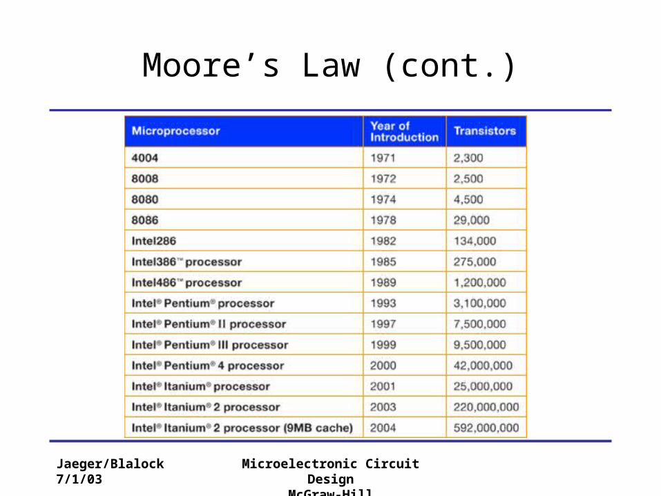
Moore’s Law (cont.)
Jaeger/Blalock7/1/03
Microelectronic Circuit DesignMcGraw-Hill

Moore’s Law (cont.)
Jaeger/Blalock7/1/03
Microelectronic Circuit DesignMcGraw-Hill

Moore’s Law (cont.)
Jaeger/Blalock7/1/03
Microelectronic Circuit DesignMcGraw-Hill

Moore’s Law (cont.)
Jaeger/Blalock7/1/03
Microelectronic Circuit DesignMcGraw-Hill

Moore’s Law (cont.)
Jaeger/Blalock7/1/03
Microelectronic Circuit DesignMcGraw-Hill

Transistor History
• Nobel prize for transistor (William Shockley) – link
• History of transistors - link
Jaeger/Blalock7/1/03
Microelectronic Circuit DesignMcGraw-Hill

Jaeger/Blalock7/1/03
Microelectronic Circuit DesignMcGraw-Hill
Types of Field-Effect Transistors
• MOSFET (Metal-Oxide Semiconductor Field-Effect Transistor)
– Primary component in high-density VLSI chips such as memories and microprocessors
• JFET (Junction Field-Effect Transistor)
– Finds application especially in analog and RF circuit design
Chap1-11

Jaeger/Blalock7/1/03
Microelectronic Circuit DesignMcGraw-Hill
MOS Capacitor Structure
• First electrode- Gate : Consists of low-resistivity material such as polycrystalline silicon
• Second electrode- Substrate or Body: n- or p-type semiconductor
• Dielectric-Silicon dioxide:stable high-quality electrical insulator between gate and substrate.
Chap1-12

Jaeger/Blalock7/1/03
Microelectronic Circuit DesignMcGraw-Hill
Substrate Conditions for Different Biases
• Accumulation
– VG<<VTN
• Depletion
– VG<VTN
• Inversion
– VG>VTN
Chap1-13

Jaeger/Blalock7/1/03
Microelectronic Circuit DesignMcGraw-Hill
Low-frequency C-V Characteristics for MOS Capacitor on P-type Substrate
• MOS capacitance is non-linear function of voltage.
• Total capacitance in any region dictated by the separation between capacitor plates.
• Total capacitance modeled as series combination of fixed oxide capacitance and voltage-dependent depletion layer capacitance.
Chap1-14

Jaeger/Blalock7/1/03
Microelectronic Circuit DesignMcGraw-Hill
NMOS Transistor: Structure
• 4 device terminals: Gate(G), Drain(D), Source(S) and Body(B).
• Source and drain regions form pn junctions with substrate.
• vSB, vDS and vGS always positive during normal operation.
• vSB always < vDS and vGS to reverse bias pn junctions
Chap1-15

Jaeger/Blalock7/1/03
Microelectronic Circuit DesignMcGraw-Hill
NMOS Transistor: Qualitative I-V Behavior
• VGS<<VTN : Only small leakage current flows.
• VGS<VTN: Depletion region formed under gate merges with source and drain depletion regions. No current flows between source and drain.
• VGS>VTN: Channel formed between source and drain. If vDS>0,, finite iD flows from drain to source.
• iB=0 and iG=0.
Chap1-16

Jaeger/Blalock7/1/03
Microelectronic Circuit DesignMcGraw-Hill
NMOS Transistor: Triode Region Characteristics
Di
DSv
2DS
vTNV
GSv
L
WnKDi
where, Kn= Kn’W/L
Kn’=μnCox’’ (A/V2)
Cox’’=εox/Tox
εox=oxide permittivity
(F/cm)
Tox=oxide thickness (cm)
for 0DS
vTNVGS
v
Chap1-17

Jaeger/Blalock7/1/03
Microelectronic Circuit DesignMcGraw-Hill
NMOS Transistor: Triode Region Characteristics (contd.)
• Output characteristics appear to be linear.
• FET behaves like a gate-source voltage-controlled resistor between source and drain with
TNVGS
VL
WnK
onR'
1
Chap1-18

Jaeger/Blalock7/1/03
Microelectronic Circuit DesignMcGraw-Hill
MOSFET as Voltage-Controlled Resistor
Example 1: Voltage-Controlled Attenuator
TNVGG
VRnKRonRonR
svov
11
If Kn=500μA/V2, VTN=1V, R=2kΩ and VGG=1.5V, then,
667.0V15.12000
2V
μA5001
1
sv
ov
To maintain triode region operation,
V)15.1(667.0 S
v or V750.0S
v
TNVGG
Vov orTNVGS
vDS
v
If Kn=500μA/V2, VTN=1V, R=2kΩ and VGG=1.5V, then,
Chap1-19

Jaeger/Blalock7/1/03
Microelectronic Circuit DesignMcGraw-Hill
MOSFET as Voltage-Controlled Resistor (contd.)
Example 2: Voltage-Controlled High-Pass Filter
Voltage Transfer function, os
sssVsoV
sT
where, cut-off frequency
CTN
VGS
VnK
ConRo)(1
If Kn=500μA/V2, VTN=1V, C=0.02μF and VGG=1.5V, then,
kHz99.1μF)02.0(2
V15.12V
μA500
of
To maintain triode region operation,V5.0 TNV
GGVsv
Chap1-20

Jaeger/Blalock7/1/03
Microelectronic Circuit DesignMcGraw-Hill
NMOS Transistor: Saturation Region
• If vDS increases above triode region limit, channel region disappears, also said to be pinched-off.
• Current saturates at constant value, independent of vDS.
• Saturation region operation mostly used for analog amplification.
Chap1-21

Jaeger/Blalock7/1/03
Microelectronic Circuit DesignMcGraw-Hill
NMOS Transistor: Saturation Region (contd.)
2
2
TNVGS
vL
WnKDi
for TNVGS
vDS
v
TNVGS
vDSAT
v is also called saturation or pinch-off voltage
Chap1-22

State of the Art – 32 nm
• Intel – power of smaller - link
• 32nm high k metal gate transistor - link
Jaeger/Blalock7/1/03
Microelectronic Circuit DesignMcGraw-Hill

Jaeger/Blalock7/1/03
Microelectronic Circuit DesignMcGraw-Hill
Transconductance of a MOS Device
• Transconductance relates the change in drain current to a change in gate-source voltage
• Taking derivative of the expression for the drain current in saturation region,
ptQGSdv
Ddimg
TNV
GSV
DI
TNVGS
VL
WnKmg
2)('
Chap1-24

Jaeger/Blalock7/1/03
Microelectronic Circuit DesignMcGraw-Hill
Channel-Length Modulation
• As vDS increases above vDSAT, length of depleted channel beyond pinch-off point, L, increases and actual L decreases.
• iD increases slightly with vDS
instead of being constant.
DS
vTNVGS
vL
WnKDi 1
2
2
channel length modulation parameter
Chap1-25

Jaeger/Blalock7/1/03
Microelectronic Circuit DesignMcGraw-Hill
Depletion-Mode MOSFETS
• NMOS transistors with
• Ion implantation process used to form a built-in n-type channel in device to connect source and drain by a resistive channel
• Non-zero drain current for vGS=0, negative vGS required to turn device off.
0TNV
Chap1-26

Jaeger/Blalock7/1/03
Microelectronic Circuit DesignMcGraw-Hill
Transfer Characteristics of MOSFETS
• Plots drain current versus gate-source voltage for a fixed drain-source voltage
Chap1-27

Jaeger/Blalock7/1/03
Microelectronic Circuit DesignMcGraw-Hill
Body Effect or Substrate Sensitivity
• Non-zero vSB changes threshold voltage, causing substrate sensitivity modeled by
where
VTO= zero substrate bias for VTN (V)
body-effect parameterF= surface potential parameter (V)
FFSBv
TOVTNV 22
V
Chap1-28
Jaeger/Blalock7/1/03
Microelectronic Circuit DesignMcGraw-Hill
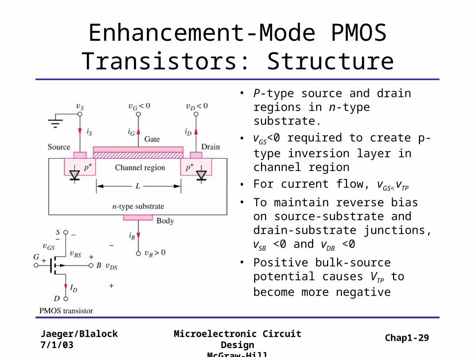
Enhancement-Mode PMOS Transistors: Structure
• P-type source and drain regions in n-type substrate.
• vGS<0 required to create p-type inversion layer in channel region
• For current flow, vGS< vTP
• To maintain reverse bias on source-substrate and drain-substrate junctions, vSB <0 and vDB <0
• Positive bulk-source potential causes VTP to become more negative
Chap1-29

Jaeger/Blalock7/1/03
Microelectronic Circuit DesignMcGraw-Hill
Enhancement-Mode PMOS Transistors: Output Characteristics
• For , transistor is off.
• For more negative vGS, drain current increases in magnitude.
• PMOS is in triode region for small values of VDS and in saturation for larger values.
TPVGS
V
Chap1-30

Jaeger/Blalock7/1/03
Microelectronic Circuit DesignMcGraw-Hill
MOSFET Circuit Symbols
• (g) and(i) are the most commonly used symbols in VLSI logic design.
• MOS devices are symmetric.
• In NMOS, n+ region at higher voltage is the drain.
• In PMOS p+ region at lower voltage is the drain
Chap1-31

40 years of Moore’s Law and CPU
• The history of microprocessor- link
• The history of intel CPU – link
• What did you do 40 years ago? - link
• 45nm : biggest change to transistor in 40 years - link
Jaeger/Blalock7/1/03
Microelectronic Circuit DesignMcGraw-Hill

Jaeger/Blalock7/1/03
Microelectronic Circuit DesignMcGraw-Hill
Process-defining Factors
• Minimum Feature Size, F : Width of smallest line or space that can be reliably transferred to wafer surface using given generation of lithographic manufacturing tools
• Alignment Tolerance, T: Maximum misalignment that can occur between two mask levels during fabrication
Chap1-33

Jaeger/Blalock7/1/03
Microelectronic Circuit DesignMcGraw-Hill
Mask Sequence for a Polysilicon-Gate Transistor
• Mask 1: Defines active area or thin oxide region of transistor
• Mask 2: Defines polysilicon gate of transistor, aligns to mask 1
• Mask 3: Delineates the contact window, aligns to mask 2.
• Mask 4: Delineates the metal pattern, aligns to mask 3.
• Channel region of transistor formed by intersection of first two mask layers. Source and Drain regions formed wherever mask 1 is not covered by mask 2
Chap1-34

Jaeger/Blalock7/1/03
Microelectronic Circuit DesignMcGraw-Hill
Basic Ground Rules for Layout
• F=2Λ
• T=F/2=could be1, 0.5, 0.25 m, etc.
Chap1-35

Jaeger/Blalock7/1/03
Microelectronic Circuit DesignMcGraw-Hill
Internal Capacitances in Electronic Devices
• Limit high-frequency performance of the electronic device they are associated with.
• Limit switching speed of circuits in logic applications
• Limit frequency at which useful amplification can be obtained in amplifiers.
• MOSFET capacitances depend on operation region and are non-linear functions of voltages at device terminals.
Chap1-36

Jaeger/Blalock7/1/03
Microelectronic Circuit DesignMcGraw-Hill
NMOS Transistor Capacitances: Triode Region
Cox” =Gate-channel capacitance per unit area(F/m2).
CGC =Total gate channel capacitance.
CGS = Gate-source capacitance.
CGD =Gate-drain capacitance.
CGSO and CGDO = overlap capacitances (F/m).
WGSO
CWLoxCW
GSOCGC
CGS
C 2
"2
WGSO
CWLoxCW
GSOCGC
CGD
C 2
"2
Chap1-37

Jaeger/Blalock7/1/03
Microelectronic Circuit DesignMcGraw-Hill
NMOS Transistor Capacitances: Triode Region (contd.)
CSB = Source-bulk capacitance.
CDB = Drain-bulk capacitance.
AS and AD = Junction bottom area capacitance of the source and drain regions.
PS and PD = Perimeter of the source and drain junction regions.
SPJSWCSAJCSBC
DPJSW
CDAJCDBC
Chap1-38

Jaeger/Blalock7/1/03
Microelectronic Circuit DesignMcGraw-Hill
NMOS Transistor Capacitances: Saturation Region
• Drain no longer connected to channel
WGSO
CGC
CGS
C 32
WGDO
CGD
C
Chap1-39

Jaeger/Blalock7/1/03
Microelectronic Circuit DesignMcGraw-Hill
NMOS Transistor Capacitances: Cutoff Region
• Conducting channel region completely gone.
CGB = Gate-bulk capacitance
CGBO = gate-bulk capacitance per unit width.
WGDO
CGD
C
WGSO
CGS
C
WGBO
CGB
C
Chap1-40

Jaeger/Blalock7/1/03
Microelectronic Circuit DesignMcGraw-Hill
SPICE Model for NMOS Transistor
Typical default values used by SPICE:
Kn or Kp = 20 A/V2
= 0
= 0
VTO = 1 V
n or p = 600 cm2/V.s
2F = 0.6 V
CGDO=CGSO=CGBO=CJSW= 0
Tox= 100 nmChap1-41

Jaeger/Blalock7/1/03
Microelectronic Circuit DesignMcGraw-Hill
Bias Analysis Approach
• Assume an operation region (generally the saturation region)
• Use circuit analysis to find VGS
• Use VGS to calculate ID, and ID to find VDS
• Check validity of operation region assumptions
• Change assumptions and analyze again if required.
NOTE :An enhancement-mode device with VDS = VGS is always in saturation
Chap1-42

Jaeger/Blalock7/1/03
Microelectronic Circuit DesignMcGraw-Hill
Constant Gate-Source MOSFET Bias Circuit

Jaeger/Blalock7/1/03
Microelectronic Circuit DesignMcGraw-Hill
Simplified MOSFET Bias Circuit

Jaeger/Blalock7/1/03
Microelectronic Circuit DesignMcGraw-Hill
Loadline Analysis

Jaeger/Blalock7/1/03
Microelectronic Circuit DesignMcGraw-Hill
Four-Resistor and Two-Resistor Biasing
• Provide excellent bias for transistors in discrete circuits.
• Stabilize bias point with respect to device parameter and temperature variations using negative feedback.
• Use single voltage source to supply both gate-bias voltage and drain current.
• Generally used to bias transistors in saturation region.
• Two-resistor biasing uses lesser components that four-resistor biasing and also isolates drain and gate terminals
Chap1-46

Jaeger/Blalock7/1/03
Microelectronic Circuit DesignMcGraw-Hill
Bias Analysis: Example 1 (Four-Resistor Biasing)
Problem: Find Q-pt (ID, VDS)
Approach: Assume operation region, find Q-point, check to see if result is consistent with operation region
Assumption: Transistor is saturated, IG=IB=0
Analysis: First, simplify circuit, split VDD into two equal-valued sources and apply Thevenin transformation to find VEQ and REQ for gate-bias voltage
Chap1-47

Jaeger/Blalock7/1/03
Microelectronic Circuit DesignMcGraw-Hill
Bias Analysis: Example 1 (Four-Resistor Biasing) (contd.)
SRDIGSVEQV Since IG=0,
2
2
TN
VGS
VSRnK
GSVEQV
21
2
4109.3610254
GS
VGSV
021.705.02 GSVGSV
V66.2,V71.2 GSV
Since VGS<VTN for VGS= -2.71 V and MOSFET will be cut-off,
V66.2GSV and ID= 34.4 A
Also, DSVSRDRDIDDV )(
V08.6 DSV
VDS>VGS-VTN. Hence saturation region assumption is correct.
Q-pt: (34.4 A, 6.08 V) with VGS= 2.66 V
Chap1-48

Jaeger/Blalock7/1/03
Microelectronic Circuit DesignMcGraw-Hill
Bias Analysis: Example 2 (Four-Resistor Biasing)
• Estimate value of ID and use it to find VGS and VSB
• Use VSB to calculate VTN
• Find ID’ using above 2 steps
• If ID’ is not same as original ID estimate, start again.
Analysis with body effect using same assumptions as in example 1:
DISRDIEQVGSV 000,226
DISRDISBV 000,22
)22(FFSB
VTOVTNV
)6.06.0(5.01 SB
VTNV
2
2
61025'
TNV
GSVDI
Iterative solution can be found by following steps:
Chap1-49

Jaeger/Blalock7/1/03
Microelectronic Circuit DesignMcGraw-Hill
Bias Analysis: Example 2 (Four-Resistor Biasing) (contd.)
The iteration sequence leads to ID= 88.0 A
V48.6000,4010)( DISRDRDIDDVDSV
VDS>VGS-VTN. Hence saturation region assumption is correct.
Q-pt: (88.0 A, 6.48 V)
Chap1-50

Jaeger/Blalock7/1/03
Microelectronic Circuit DesignMcGraw-Hill
VDD
REQ
RD
V EQ I
G RS
IDS
4 V
60 k
75 k
10 V+
-
+
-VGS
VDS
DG
S
39 k
+
-
VS

Jaeger/Blalock7/1/03
Microelectronic Circuit DesignMcGraw-Hill
Four Transistor Bias Summary
VEQ = VGS + IDS RS (4.48)
VDD = IDS RD + VDS + IDS RS (4.50)
IDS VGS IDS
VDS IDS VGS IDS VDS
Assume that the transistor is operating in the saturation region with
IDS = Kn/2 (VGS – VTN)2 (4.47)

Jaeger/Blalock7/1/03
Microelectronic Circuit DesignMcGraw-Hill
VEQ=VGS+ RsKn/2 (VGS – VTN)2 (4.49)
Solve VGS and check to make sure transistor is not cutoff.
Use (4.53) to compute IDS, (4.52) to get VDS
Verify that transistor is in saturation mode because VDS ≥ VGS-VTN

Jaeger/Blalock7/1/03
Microelectronic Circuit DesignMcGraw-Hill
Bias Analysis: Example 3 (Two-Resistor Biasing)
Assumption: IG=IB=0, transistor is saturated (since VDS= VGS)
Analysis:
DRDIDDVDSV
2
2
TN
VGS
VDRnK
DDVGSV
21
2
4104106.23.3
GSVGSV
V00.2,V769.0 GSV
Since VGS<VTN for VGS= -0.769 V and MOSFET will be cut-off,
V00.2GSV and ID= 130 A
VDS>VGS-VTN. Hence saturation region assumption is correct.
Q-pt: (130 A, 2.00 V)
Chap1-54

Jaeger/Blalock7/1/03
Microelectronic Circuit DesignMcGraw-Hill
Bias Analysis: Example 4 ( Biasing in Triode Region)
Assumption: IG=IB=0, transistor is saturated (since VDS= VGS)
Analysis: VGS=VDD=4 V
mA13.12)14(2V
μA2
250 DI
DSVDRDIDDV )(Also
V19.2 DSV
But VDS<VGS-VTN. Hence, saturation region assumption is incorrect Using triode region equation,
DSVDI 16004
DSVDSV
DSV )2
14(2V
μA2
25016004
V3.2 DSV and ID=1.06 mA
VDS<VGS-VTN, transistor is in triode region
Q-pt:(1.06 mA, 2.3 V)
Chap1-55

Jaeger/Blalock7/1/03
Microelectronic Circuit DesignMcGraw-Hill
Bias Analysis: Example 5 (Two-Resistor biasing for PMOS Transistor)
Assumption: IG=IB=0, transistor is saturated (since VDS= VGS)
Analysis:0)kΩ470( DSVGIGSV
Also 0)kΩ220(V15 DSVDI
02
22V
μA2
50)kΩ220(V15
GSV
GSV
V45.3,V369.0 GSV
Since VGS= -0.369 V is less than VTP= -2 V, VGS = -3.45 V
ID = 52.5 A and VGS = -3.45 V
Hence saturation assumption is correct.
Q-pt: (52.5 A, -3.45 V)
TPVGSVDSV
Chap1-56

Jaeger/Blalock7/1/03
Microelectronic Circuit DesignMcGraw-Hill
Feedback Analysis
• Negative Feedback is used to stabilize the operating point.
• ID -VDS -VGS ID

Jaeger/Blalock7/1/03
Microelectronic Circuit DesignMcGraw-Hill
MOSFET as Current Source
• Ideal current source gives fixed output current regardless of voltage across it.
• MOSFET behaves as as an ideal current source if biased in the pinch-off region (output current depends on terminal voltage).
Chap1-58

Jaeger/Blalock7/1/03
Microelectronic Circuit DesignMcGraw-Hill
NMOS Current Mirror
Assumption: M1 and M2 have identical VTN, Kn’, and W/L and are in saturation.
DS1VTNVGS1V
L
WnKREFI 1
2
2
DS2VTNVGS2V
L
WnK
OI 12
2
But VGS2=VGS1
REFI
DS1V
DS2V
REFIOI
1
1
Thus, output current mirrors reference current if VDS1=VDS2.
Chap1-59
Jaeger/Blalock7/1/03
Microelectronic Circuit DesignMcGraw-Hill
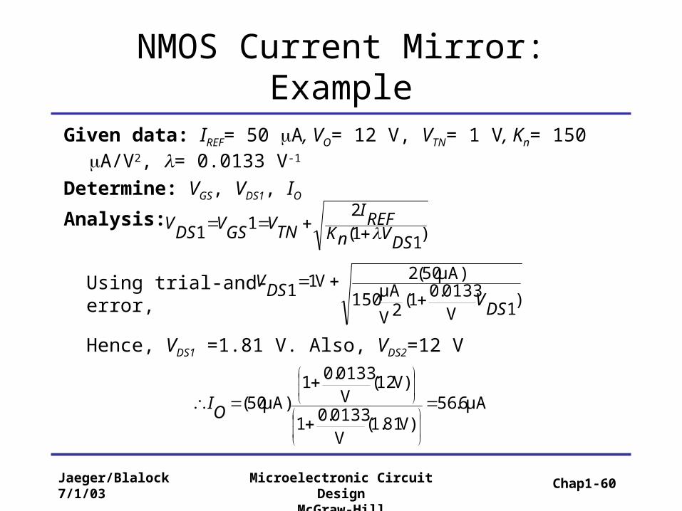
NMOS Current Mirror: Example
Given data: IREF= 50 A, VO= 12 V, VTN= 1 V, Kn= 150 A/V2, = 0.0133 V-1
Determine: VGS, VDS1, IO
Analysis:)11(
211
DSVnKREFI
TNVGSVDSV
Using trial-and-error,)1V
0133.01(2V
μA150
)μA50(2V11DSV
DSV
Hence, VDS1 =1.81 V. Also, VDS2=12 V
μA6.56V)81.1(
V0133.01
V)12(V0133.01
)μA50(
OI
Chap1-60

Jaeger/Blalock7/1/03
Microelectronic Circuit DesignMcGraw-Hill
MOS Current Mirror Ratio
'21
'1 nKL
WnKnK
'102
'2 nKL
WnKnK
DS1V
DS2V
REFI
DS1V
DS2V
LWLW
REFIOI
1
15
1
1
1/2/
REFIOI 5
Thus, ratio between IO and IREF can be modified by changing W/L ratios of the current mirror transistors (ignoring differences due to VDS
mismatch)
Chap1-61

Jaeger/Blalock7/1/03
Microelectronic Circuit DesignMcGraw-Hill
MOS Current Mirror Output Resistance
• Output current changes with vDS due to channel length modulation.
• Output resistance is given by
• In the current mirror, vO = vDS2
1
ptQOvOi
OR
O
vTNVGS2
vL
WnKOi 1
2
2
OI
OI
OV
OV
OI
OR
111
1
Chap1-62

Jaeger/Blalock7/1/03
Microelectronic Circuit DesignMcGraw-Hill
Current Mirror Layout
Two possible layouts of a current mirror
Chap1-63

Jaeger/Blalock7/1/03
Microelectronic Circuit DesignMcGraw-Hill
Design of Multiple Current Mirrors: Example
μA50
1/2/
2 LWLW
REFIDI
μA125
1/3/
3 LWLW
REFIDI
μA25
4/5/
5 LWLW
REFIDI
Choose R to set IREF= 25 A
REFIGSNVGSPV
R
10
Chap1-64

Jaeger/Blalock7/1/03
Microelectronic Circuit DesignMcGraw-Hill
Design of Multiple Current Mirrors (contd).
kΩ274μAV
2545.171.110 R
V71.12
pKDI
TPVGSPV V45.12
nKDI
TNVGSNVand
R can be replaced by transistor M6 for better integration. We know that VGS6 = -6.84 V and ID = 25 A and M6 is in saturation
22
'
TPVGSVL
WpKDI
6.13
1
LW
Chap1-65

Jaeger/Blalock7/1/03
Microelectronic Circuit DesignMcGraw-Hill
MOS Transistor Scaling
• Drain current:
• Gate Capacitance:
where is the circuit delay in a logic circuit.
nKL
WoxTox
nLW
oxTox
nnK
//
/*
DiDS
vDSv
TNv
GSv
LW
oxTox
nDi
2//
/*
GC
C
LW
oxToxLWoxC
GCC
//
/***)"(*
//
*
***
DiVGC
C
DiV
GCC
Chap1-66

Jaeger/Blalock7/1/03
Microelectronic Circuit DesignMcGraw-Hill
MOS Transistor Scaling (contd.)
• Circuit and Power Densities:
• Power-Delay Product:
• Cutoff Frequency:
fT improves with square of channel length reduction
2***
PDiDDV
DiDDVP
AP
LW
PLW
P
LW
P
A
P )/)(/(
2/**
*
*
*
32***
PDPPPPDP
TNVGS
VLn
GCC
mgTf 22
121
Chap1-67

Jaeger/Blalock7/1/03
Microelectronic Circuit DesignMcGraw-Hill
MOS Transistor Scaling (contd.)
• High Field Limitations:
– High electric fields arise if technology is scaled down with supply voltage constant.
– Cause reduction in mobility of MOS transistor, breakdown of linear relationship between mobility and electric field and carrier velocity saturation.
– Ultimately results in reduced long-term reliability and breakdown of gate oxide or pn junction.
– Drain current in saturation region is linearised to
SATvTNv
GSv
WoxCDi )(
2" where, vSAT is carrier
saturation velocity
Chap1-68

Jaeger/Blalock7/1/03
Microelectronic Circuit DesignMcGraw-Hill
MOS Transistor Scaling (contd.)
• Sub-threshold Conduction:– ID decreases exponentially for
VGS<VTN.
– Reciprocal of the slope in mV/decade gives the turn off rate for the MOSFET.
– VTN should be reduced if dimensions are scaled down, but curve in sub-threshold region shifts horizontally instead of scaling with VTN..
Chap1-69

Jaeger/Blalock7/1/03
Microelectronic Circuit DesignMcGraw-Hill
MOS Scaling
Jaeger/Blalock7/1/03
Microelectronic Circuit DesignMcGraw-Hill
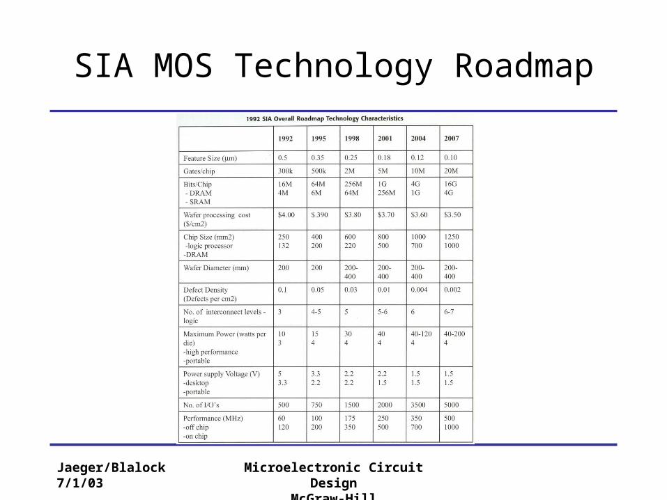
SIA MOS Technology Roadmap

Jaeger/Blalock7/1/03
Microelectronic Circuit DesignMcGraw-Hill
Worldwide Semiconductor Sales Trend

Jaeger/Blalock7/1/03
Microelectronic Circuit DesignMcGraw-Hill
Technology Cross-over

Jaeger/Blalock7/1/03
Microelectronic Circuit DesignMcGraw-Hill
Linear Technology Shrink

Jaeger/Blalock7/1/03
Microelectronic Circuit DesignMcGraw-Hill
MOS Technology Scaling Ratio

Jaeger/Blalock7/1/03
Microelectronic Circuit DesignMcGraw-Hill
Linear Shrink
• Cost Per Function : 40% reduction

Jaeger/Blalock7/1/03
Microelectronic Circuit DesignMcGraw-Hill
Re-Design Scale Factors

Jaeger/Blalock7/1/03
Microelectronic Circuit DesignMcGraw-Hill
Intel CPU Scaling

Jaeger/Blalock7/1/03
Microelectronic Circuit DesignMcGraw-Hill
Wafer Diameter Increase

Jaeger/Blalock7/1/03
Microelectronic Circuit DesignMcGraw-Hill
Dies on a Wafer

Jaeger/Blalock7/1/03
Microelectronic Circuit DesignMcGraw-Hill
Gross Die Per Wafer

Jaeger/Blalock7/1/03
Microelectronic Circuit DesignMcGraw-Hill
Gate Cost
• Die Size too small – I/O overhead• Die Size too big - Complexity

Jaeger/Blalock7/1/03
Microelectronic Circuit DesignMcGraw-Hill
Gate Cost
• Pentium 4 has 14M Gates – Near Optimum

Jaeger/Blalock7/1/03
Microelectronic Circuit DesignMcGraw-Hill

Jaeger/Blalock7/1/03
Microelectronic Circuit DesignMcGraw-Hill

Jaeger/Blalock7/1/03
Microelectronic Circuit DesignMcGraw-Hill

Jaeger/Blalock7/1/03
Microelectronic Circuit DesignMcGraw-Hill

Jaeger/Blalock7/1/03
Microelectronic Circuit DesignMcGraw-Hill

Jaeger/Blalock7/1/03
Microelectronic Circuit DesignMcGraw-Hill

Jaeger/Blalock7/1/03
Microelectronic Circuit DesignMcGraw-Hill

Jaeger/Blalock7/1/03
Microelectronic Circuit DesignMcGraw-Hill

Jaeger/Blalock7/1/03
Microelectronic Circuit DesignMcGraw-Hill

Jaeger/Blalock7/1/03
Microelectronic Circuit DesignMcGraw-Hill

Jaeger/Blalock7/1/03
Microelectronic Circuit DesignMcGraw-Hill

Jaeger/Blalock7/1/03
Microelectronic Circuit DesignMcGraw-Hill

Jaeger/Blalock7/1/03
Microelectronic Circuit DesignMcGraw-Hill

Jaeger/Blalock7/1/03
Microelectronic Circuit DesignMcGraw-Hill

Jaeger/Blalock7/1/03
Microelectronic Circuit DesignMcGraw-Hill
Junction Field-Effect Transistor (JFET) Structure
• Much lower input current and much higher input impedance than BJT.
• In triode region, JFET is a voltage-controlled resistor,
= resistivity of channel
L = channel length
W = channel width between pn junction depletion regions
t = channel depth
• Inherently a depletion-mode device
• N-type semiconductor block that houses the channel region in n-channel JFET.
• Two pn junctions to form the gate.
• Current enters channel at drain and exits at source.
WL
tCHR
Chap1-98

Jaeger/Blalock7/1/03
Microelectronic Circuit DesignMcGraw-Hill
JFET with Gate-Source Bias
• vGS =0, gate isolated from channel.
• VP < vGS <0, W’<W, channel resistance increases, gate-source junction reverse-biased, iG almost 0.
• vGS = VP <0, channel region pinched-off, channel resistance infinite.
Chap1-99

Jaeger/Blalock7/1/03
Microelectronic Circuit DesignMcGraw-Hill
JFET Channel with Drain-Source Bias
• With constant vGS, depletion region near drain increases with vDS.
• At vDSP = vGS - VP,channel is totally pinched-off, iD is saturated.
• JFET also suffers from channel length modulation like MOSFET at larger values of vDS.
Chap1-100

Jaeger/Blalock7/1/03
Microelectronic Circuit DesignMcGraw-Hill
N-Channel JFET: i-v Characteristics
Transfer Characteristics Output Characteristics
Chap1-101

Jaeger/Blalock7/1/03
Microelectronic Circuit DesignMcGraw-Hill
N-Channel JFET: i-v Characteristics (contd.)
• For all regions : iG=0 for
• In cutoff region: iD =0 for (VP <0).
• In Triode region:
for and
• In pinch-off region:
for
0GS
v
PVGS
v
DSvDS
v
PV
GSv
PV
DSSI
Di2
22
2
PVGS
v 0DS
vPVGS
v
DS
v
PVGS
v
DSSIDi 1
2
1 0 PVGS
vDS
v
Chap1-102

Jaeger/Blalock7/1/03
Microelectronic Circuit DesignMcGraw-Hill
P-Channel JFET
• Polarities of n- and p-type regions of n-channel JFET are reversed to get the p-Channel JFET.
• Channel current direction and operating bias voltages are also reversed.
Chap1-103

Jaeger/Blalock7/1/03
Microelectronic Circuit DesignMcGraw-Hill
JFET Circuit Symbols
• JFET structures are symmetric like MOSFET.
• Source and drain determined by circuit voltages.
Chap1-104

Jaeger/Blalock7/1/03
Microelectronic Circuit DesignMcGraw-Hill
JFET Capacitances and SPICE Modeling
• CGD and CGS are determined by depletion-layer capacitances of reverse-biased pn junctions forming gate and are bias dependent.
• Typical default values used by SPICE:
Vp = -2 V
= CGD = CGD =0
Transconductance parameter= BETA =IDSS/VP
2= 100 A/V2
Chap1-105

Jaeger/Blalock7/1/03
Microelectronic Circuit DesignMcGraw-Hill
Biasing JFET and Depletion-Mode MOSFET: Example
• Assumptions: JFET is pinched-off, gate-channel junction is reverse-biased, reverse leakage current of gate, IG = 0
N-channel JFET Depletion-mode MOSFET
Chap1-106

Jaeger/Blalock7/1/03
Microelectronic Circuit DesignMcGraw-Hill
Biasing JFET and Depletion-Mode MOSFET: Example (contd.)
• Analysis: Since IS = ID , SRDIGSV
2
V511000A3105
2
1
GS
V
PVGS
V
SRDSSIGSV
V1.13,V91.1 GSV
Since VGS= -13.1 V is less than VP= -5 V, VGS = -1.91 V and, ID = IS = 1.91 mA. Also,
V27.6)kΩ3)(mA91.1(12)( SRDRDIDDVDSV
VDS>VGS-VP. Hence pinch-off region assumption is correct and gate-source junction is reverse-biased by 1.91V.
Q-pt: (1.91 mA, 6.27 V)
Chap1-107

Jaeger/Blalock7/1/03
Microelectronic Circuit DesignMcGraw-Hill
Homework
• 4.22
• 4.81
• 4.85(a)
• 4.103(b)
• 4.145