Embed Size (px)
Citation preview
Novel Structure, Ultra-Thin CdS:O/CdTe Thin Film Solar Cells by Magnetron
Sputtering
Mohammad Aminul Islam
Ph.D Student
Supervisor: Prof. Dr. Nowshad Amin
Solar Energy Research Institute (SERI)Universiti Kebangsaan Malaysia, Malaysia
*Outline INTRODUCTION
CdS/CdTe SOLAR CELLS: SHORT REVIEW
ZnO:Sn THIN FILMS
CdS:O THIN FILMS
CdTe THIN FILMS
CdS:O/CdTe SOLAR CELLS
CONCLUSION
2

* Introduction
Cadmium Telluride Solar Cells
Glass Superstrate
Transparent Conducting Oxide N-type CdS
P-type CdTe
MetalBack Contact: Cathode
Front Contact: Anode
Window Layer
Absorber layer
Incident Light
3~8 um
0.1 um0.05 um
~1000 um
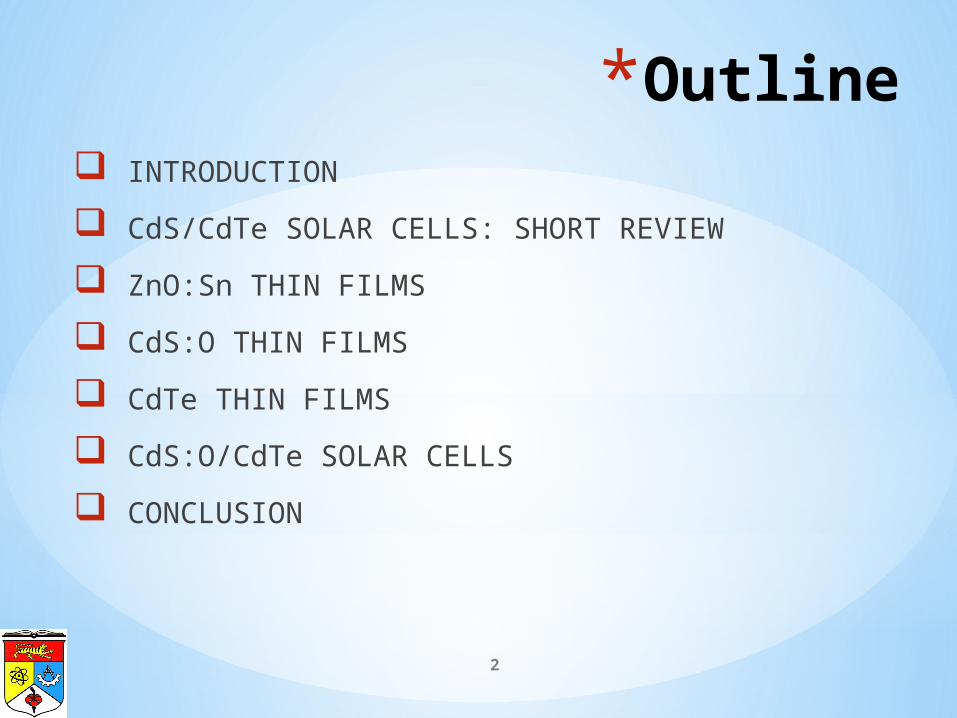
• Direct bandgap, Eg=1.45eV• Good efficiency (Record:17.3%, & 19.6%)• High module production speed• Long term stability (20 years)• Process flexibility (PVD,CVD,CBD,CSS etc)• Less material use (1µm CdTe absorbed light compared with around
10µm of Si). 3
4
* CdS/CdTe SOLAR CELLS: SHORT REVIEW

Place of CdTe as a Solar Cell Material CandidatePlace of CdTe as a Solar Cell Material Candidate
Bandgap (eV)
Eff
icie
ncy
(%
)
Solar cell efficiency vs. Bandgap
CdTeT= 300K
AM0
AM1. 5
Ge
SiCu2S
GaAs
a- Si :H:Fa- Si :H
CdS
Black-bo dy Li mi t (AM0)
0.5 1.0 1.5 2.0 2.55
10
15
20
25
30
35
Ab
sorp
tio
n C
oef
fici
ent a
(cm
-1)
Photon Energy (eV)
Absorption coefficient spectrum of principal semiconductors for solar
cells5
* CdS/CdTe SOLAR CELLS: SHORT REVIEW

Place of CdTe Solar Cell as a commercial production and market sharePlace of CdTe Solar Cell as a commercial production and market share
6
* CdS/CdTe SOLAR CELLS: SHORT REVIEW
Market Share by Technology in 2013

Production Capacity of CdTe and Other Thin Film Solar Cell Until 2017 (MW)Production Capacity of CdTe and Other Thin Film Solar Cell Until 2017 (MW)
7
After the huge growth expectations of TF technologies some years ago, the competing market price of c-Si has slowed the development of TF.
The predominant c-Si technology is maintained its market share of around 80%, because of the maturity of the technology and also because of the existing and growing capacity in China and APAC countries, which favour wafer-based technologies.
The TF technologies are expected to grow anyway at a lower rate, and therefore will stabilize their market share over the next five years.
* CdS/CdTe SOLAR CELLS: SHORT REVIEW

CdTe Solar Cell Market share ExperienceCdTe Solar Cell Market share Experience
8
* CdS/CdTe SOLAR CELLS: SHORT REVIEW
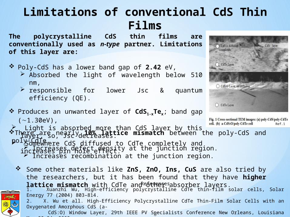
The polycrystalline CdS thin films are conventionally used as n-type partner. Limitations of this layer are:
Poly-CdS has a lower band gap of 2.42 eV, Absorbed the light of wavelength below 510 nm, responsible for lower Jsc & quantum efficiency (QE).
Produces an unwanted layer of CdS1-xTex; band gap (1.30eV), Light is absorbed more than CdS layer by this layer, so, Jsc
decreases. Somewhere CdS diffused to CdTe completely and increases
pin hole effect.
Limitations of conventional CdS Thin Films
There are nearly 10% lattice mismatch between the poly-CdS and poly-CdTe. Increases defect density at the junction region. Increases recombination at the junction region.
Some other materials like ZnS, ZnO, Ins, CuS are also tried by the researchers, but it has been found that they have higher lattice mismatch with CdTe and other absorber layers.
References1. Xuanzhi Wu, High-efficiency polycrystalline CdTe thin-film solar cells, Solar Energy 77 (2004) 803–814.2. X. Wu et all. High-Efficiency Polycrystalline CdTe Thin-Film Solar Cells with an Oxygenated Amorphous CdS (a- CdS:O) Window Layer, 29th IEEE PV Specialists Conference New Orleans, Louisiana May 20-24, 2002.3. Yan et al. The Effects of Oxygen on Junction Properties in CdS/CdTe Solar Cells, NCPV Program Review Meeting Lakewood, Colorado, 14-17 October 2001.
9
Ref.1

The oxygenated cadmium sulfide (CdS:O) window layer looks promising and might overcome the problems of CdTe based solar cells mentioned above.
CdS:O window material have broad energy band gap from 2.42 eV to 3.1 eV.
It has better lattice match with CdTe absorber layer.
It permits light spectra below wavelength 510 nm to go to the CdTe absorber layer, resulting a noticeable increase of Jsc.
Due to CdS:O layer, CdS(1-x)Ox alloy nano-particles forms at the junction of CdTe and CdS:O layers while increase crystallinity of CdTe.
Oxygenated CdS (a-CdS:O)
References1. Xuanzhi Wu, High-efficiency polycrystalline CdTe thin-film solar cells, Solar Energy 77 (2004) 803–814.2. Yan et al. The Effects of Oxygen on Junction Properties in CdS/CdTe Solar Cells, NCPV Program Review Meeting Lakewood, Colorado, 14-17 October 2001.3. Zhang et al. Raman Studies of Nanocrystalline CdS:O Film, DOE Solar Energy Technologies Program Review Meeting October 25-28, 2004 Denver, Colorado.
10

Fig. Proposed CdS:O/CdTe Solar Cells
Proposed CdS:O/CdTe Solar Cells
11

ZnO:Sn THIN FILMS FROM CO-SPUTTERING
Fig. : XRD, SEM and bandgap of ZnO:Sn thin film (RF power, ZnO: 3 watt/cm2 & Sn 0.5 watt/cm2)
The film is polycrystalline hexagonal wurtzite structured, ZnO with most prominent peak along with (002) plane confirmed by JCPDS no. 01-089-1397.
The SEM image shows that the Sn doped ZnO nanoparticles are homogeneous in nature with particle size of less than10 nm.
The band gap of the film has been found as 3.49 eV.
The carrier mobility 12.3 x 10⁻⁴ cm2/V-s was found for as-deposited film, it increased to 896.1 x 10⁻⁴ cm2/V-s with the carrier concentration and resistivity in the rang of 1018 cm-3 and kΩ-cm, respectively.
The films are prepared at 300 oC, with a pressure of 14 mTorr by continuous Ar gas flow of 10 SCCM.
12

Fig. EDX diffraction patterns of CdS:O thin films prepared in argon-oxygen ambient
Sample ID
RF power (watt/cm2)
O2 partial pressure
Cd(at.%)
S(at.%)
O(at.%)
A1 1.50 (*XPS) 0.18mTorr
29.55 28.80 41.65B1 1.75 28.65 30.48 40.87C1 2.00 34.31 34.92 30.77D1 2.15 36.74 36.31 26.95
Composition of CdS:O thin films prepared in argon-oxygen ambient
The films prepared with low deposition power incorporate the maximum amount of oxygen.
CdS:O THIN FILMS FROM REACTIVE SPUTTERINGCompositional Analysis

CdS:O THIN FILMS FROM REACTIVE SPUTTERINGX-ray Photoelectron Spectroscopy (XPS) Analysis
Fig. XPS images of CdS:O thin films prepared in argon-oxygen ambient (deposition power 1.5 watt/cm2 )14
Peak B.E, eV FWHM, eV Atomic conc. , %Cd 3d 405.6 0.946 33.57S 2p 161.2 0.731 28.38O 1s 531.9 1.610 38.05
Quantification of the compositions
The oxygen are only contributed to form SO3 or SO4 complexes.
As the oxygen content in the films increases, the coordinate number of the nearest S shell around Cd decreases, as a result, local disorder increases and the films loses its crystallinity.
CdS:O THIN FILMS FROM REACTIVE SPUTTERING
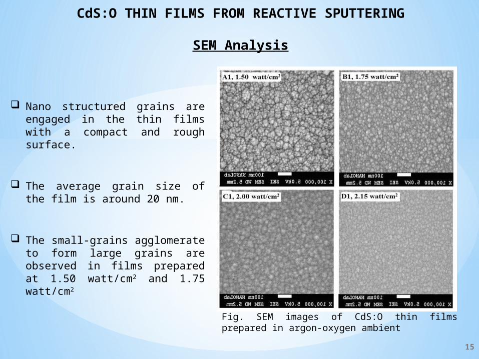
SEM Analysis
Fig. SEM images of CdS:O thin films prepared in argon-oxygen ambient
Nano structured grains are engaged in the thin films with a compact and rough surface.
The average grain size of the film is around 20 nm.
The small-grains agglomerate to form large grains are observed in films prepared at 1.50 watt/cm2 and 1.75 watt/cm2
15
CdS:O THIN FILMS FROM REACTIVE SPUTTERINGXRD and UV-Vis Analysis
Fig. XRD diffraction patterns of CdS:O filmsFig. Absorption spectra and Bandgap evaluation graph (inset) of CdS:O thin films
RF powerWatt/cm2
Peak height of
(111)(a.u)
FWHM (radian)
Crystallite size (D)
(nm)
Dislocation density
ε (x 10 -3)
Strainδ
(x 10 -3)
1.50 - - - - -
1.75 - - - - -2.00 82 0.00872 17.58 4.35 3.23
2.15 215 0.00437 25.22 2.18 0.81
RF power
Watt/cm2
Band gap(eV)
Resistivity
(x 102)(Ω-cm)
Carrier concentratio
n (x1014) /(cm-3)
Mobility(cm2/V-s)
1.50 2.723 64.4 44.78 2.161.75 2.705 54.2 32.22 3.122.00 2.682 16.4 12.21 3.312.15 2.668 42.6 41.23 3.68
Table: Bandgap and electrical properties of CdS:O thin films prepared in argon-oxygen ambient with different RF power
Table: FWHM, crystalline size, dislocation density and strain of CdS:O thin films prepared in argon-oxygen ambient
O2 composition
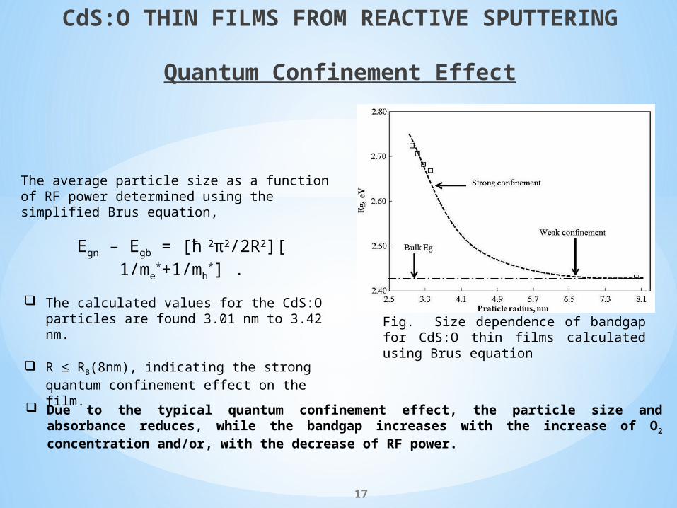
Fig. Size dependence of bandgap for CdS:O thin films calculated using Brus equation
The average particle size as a function of RF power determined using the simplified Brus equation,
Egn – Egb = [ħ 2π2/2R2][ 1/me*+1/mh
*] .
Due to the typical quantum confinement effect, the particle size and absorbance reduces, while the bandgap increases with the increase of O2 concentration and/or, with the decrease of RF power.
CdS:O THIN FILMS FROM REACTIVE SPUTTERING
Quantum Confinement Effect
17
The calculated values for the CdS:O particles are found 3.01 nm to 3.42 nm.
R ≤ RB(8nm), indicating the strong quantum confinement effect on the film.
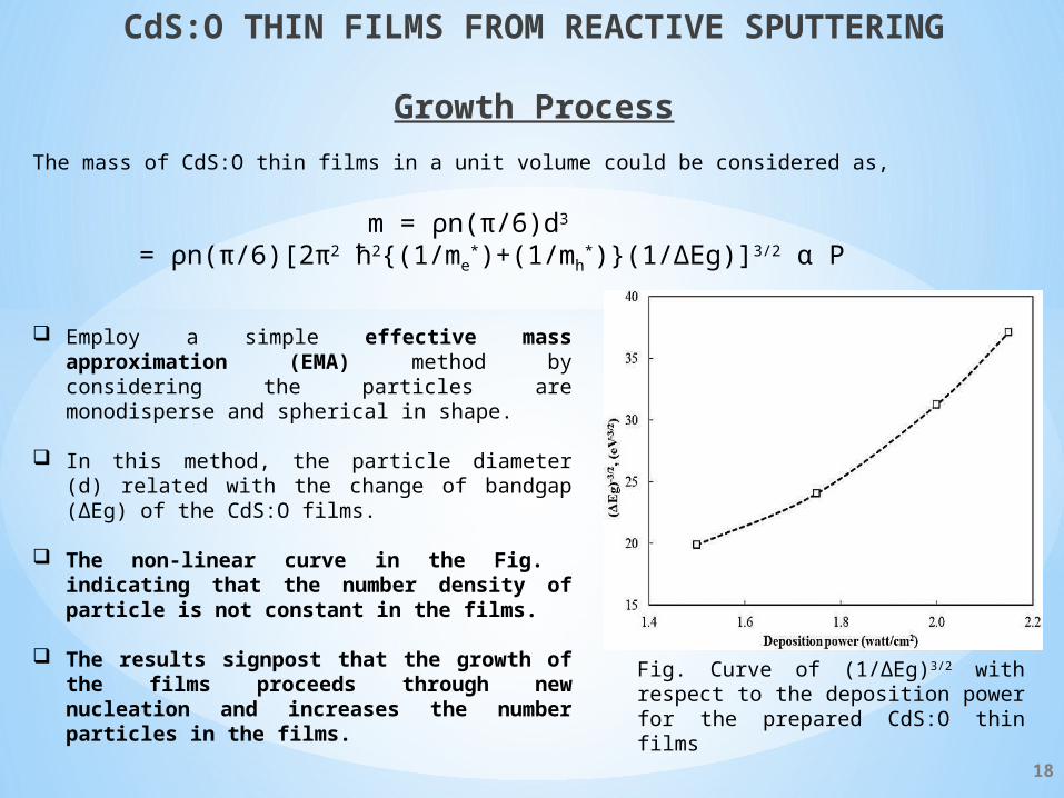
The mass of CdS:O thin films in a unit volume could be considered as,
m = ρn(π/6)d3
= ρn(π/6)[2π2 ħ2(1/me*)+(1/mh
*)(1/ΔEg)]3/2 α P
CdS:O THIN FILMS FROM REACTIVE SPUTTERING
Growth Process
Fig. Curve of (1/ΔEg)3/2 with respect to the deposition power for the prepared CdS:O thin films
Employ a simple effective mass approximation (EMA) method by considering the particles are monodisperse and spherical in shape.
In this method, the particle diameter (d) related with the change of bandgap (ΔEg) of the CdS:O films.
The non-linear curve in the Fig. indicating that the number density of particle is not constant in the films.
The results signpost that the growth of the films proceeds through new nucleation and increases the number particles in the films.
18
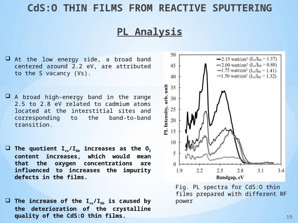
Fig. PL spectra for CdS:O thin films prepared with different RF power
At the low energy side, a broad band centered around 2.2 eV, are attributed to the S vacancy (Vs).
A broad high-energy band in the range 2.5 to 2.8 eV related to cadmium atoms located at the interstitial sites and corresponding to the band-to-band transition.
The quotient Ivs/Ibb increases as the O2 content increases, which would mean that the oxygen concentrations are influenced to increases the impurity defects in the films.
The increase of the Ivs/Ibb is caused by the deterioration of the crystalline quality of the CdS:O thin films.
CdS:O THIN FILMS FROM REACTIVE SPUTTERING
PL Analysis
19

CdTe THIN FILMSCdTe film deposition at 300 oC with ambient pressure 10 mT
20
Sample ID Dep. power Cryst. Size, D (nm) I(111)/I(220) Micro strain, ε (x 10 -3) Dislocation density, δ
as-grown/treated 1.0 watt/cm2 50.99/104.86 12.42/0.94 3.27/1.59 3.59/0.97 (x1011 cm-2)
as-grown/treated 1.5 watt/cm2 52.26/101.04 16.11/0.30 3.19/1.65 3.59/0.92 (x1011 cm-2)
as-grown/treated 2.0 watt/cm2 42.86/93.66 22.22/0.31 3.89/1.78 5.31/1.05 (x1011 cm-2)
as-grown/treated 2.5 watt/cm2 56.71/127.3 37.55/0.57 2.94/1.31 3.01/0.67 (x1011 cm-2)
as-grown/treated 3.0 watt/cm2 55.76/114.98 36.74/16.25 2.99/1.45 3.15/1.82 (x1011 cm-2)
Table : Calculated value of the structural parameters of CdTe thin films prepared by sputtering technique with variation of RF power
RF power varies from 1.0 watt/cm2 to 3.0 watt/cm2
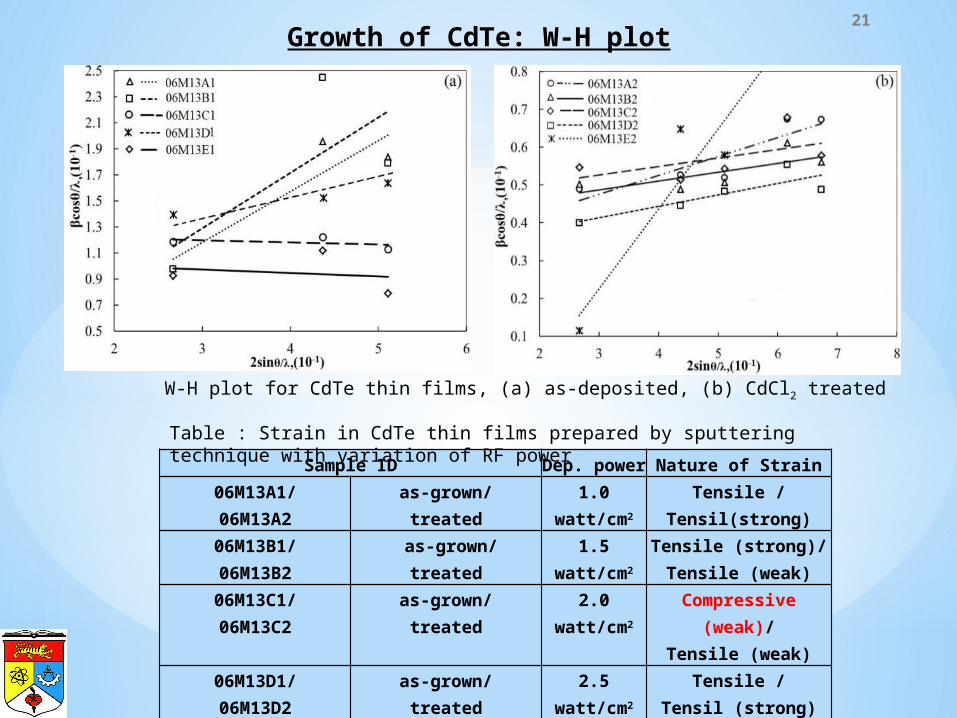
Growth of CdTe: W-H plot21
Sample ID Dep. power Nature of Strain06M13A1/06M13A2
as-grown/treated
1.0 watt/cm2 Tensile /Tensil(strong)
06M13B1/06M13B2
as-grown/treated
1.5 watt/cm2 Tensile (strong)/Tensile (weak)
06M13C1/06M13C2
as-grown/treated
2.0 watt/cm2 Compressive (weak)/Tensile (weak)
06M13D1/06M13D2
as-grown/treated
2.5 watt/cm2 Tensile /Tensil (strong)
06M13E1/06M13E2
as-grown/treated
3.0 watt/cm2 Compressive (weak)/Tensile (strong)
Table : Strain in CdTe thin films prepared by sputtering technique with variation of RF power
W-H plot for CdTe thin films, (a) as-deposited, (b) CdCl2 treated
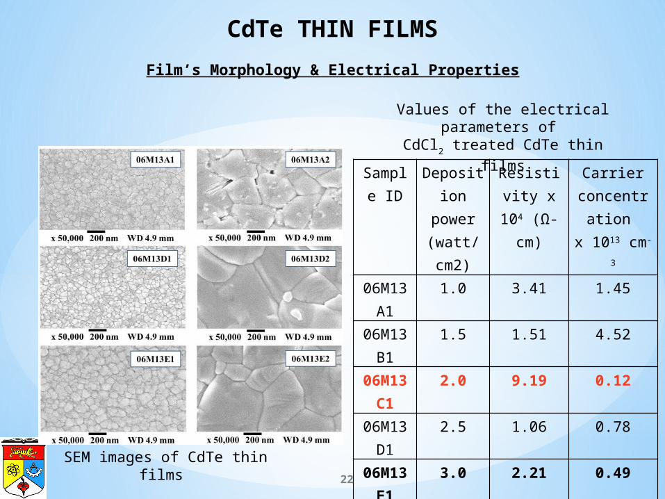
CdTe THIN FILMS
Film’s Morphology & Electrical Properties
Sample ID
Deposition power
(watt/cm2)
Resistivity x 104 (Ω-cm)
Carrier concentration
x 1013 cm-3
06M13A1 1.0 3.41 1.4506M13B1 1.5 1.51 4.5206M13C1 2.0 9.19 0.1206M13D1 2.5 1.06 0.7806M13E1 3.0 2.21 0.4906M13A2 1.0 2.68 2.2406M13B2 1.5 4.43 10.4306M13C2 2.0 1.24 13.4506M13D2 2.5 1.59 7.3006M13E2 3.0 1.61 68.69**
Values of the electrical parameters of CdCl2 treated CdTe thin films
SEM images of CdTe thin films 22

CdS:O/CdTe Solar Cells
The complete CdTe thin film solar cells has been fabricated from FTO/ZnO:Sn/CdS:O/CdTe stack with the following parameters:
Cu doped Carbon paste has been employed as a back contact of the solar cell and finally Silver paste is used as a front and back electrode.
Layers Ambient Substrate temperature
Working pressure
RF power (watt/cm2)
Deposition time, min
Approximate thickness
ZnO:Sn Ar 300 oC 14 mT 3.0:1.0 30 200 nmCdS:O Ar:O2 (99:1) RT 14 mT 1.5 30 200 nmCdTe Ar 300 oC 14 mT 1.0/2.0/2.5/3.0 100/60/50/40 1200 nm
23
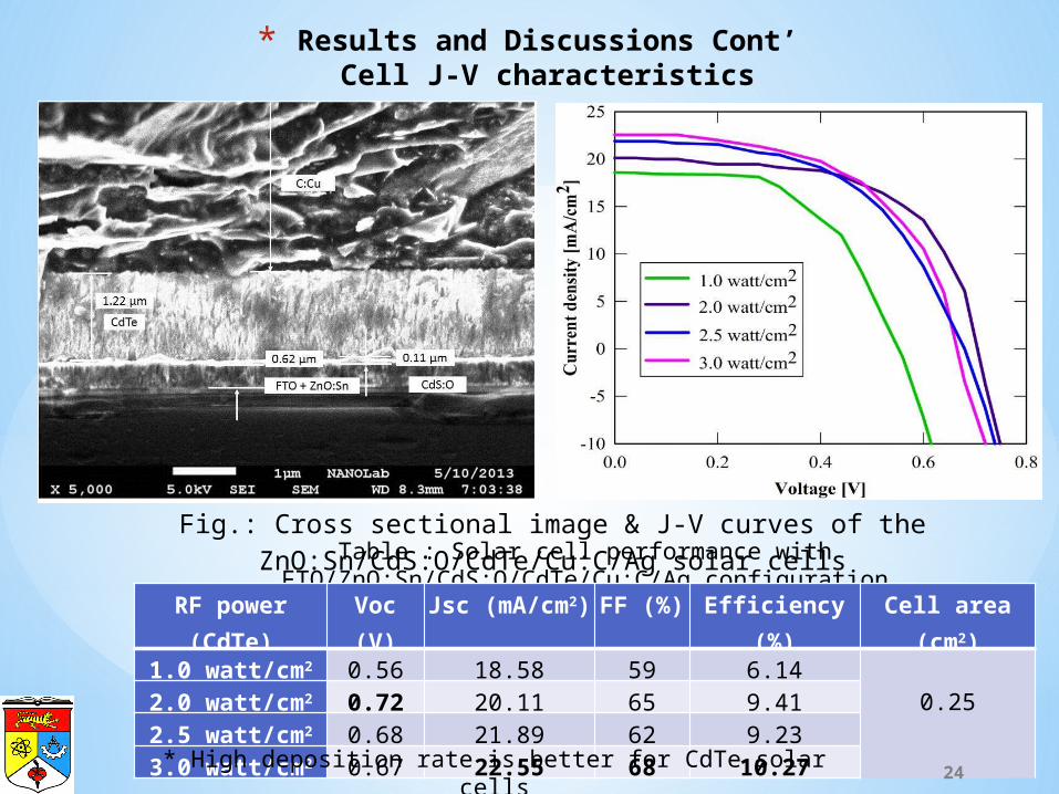
* Results and Discussions Cont’Cell J-V characteristics
Table : Solar cell performance with FTO/ZnO:Sn/CdS:O/CdTe/Cu:C/Ag configurationRF power (CdTe) Voc (V) Jsc (mA/cm2) FF (%) Efficiency (%) Cell area (cm2)
1.0 watt/cm2 0.56 18.58 59 6.140.252.0 watt/cm2 0.72 20.11 65 9.41
2.5 watt/cm2 0.68 21.89 62 9.233.0 watt/cm2 0.67 22.55 68 10.27
Fig.: Cross sectional image & J-V curves of the ZnO:Sn/CdS:O/CdTe/Cu:C/Ag solar cells
24* High deposition rate is better for CdTe solar cells
* Conclusion
The conversion efficiency as high as 10.27% with performance parameters of Voc = 0.67 Volt, Jsc = 22.55 mA/cm2; and FF = 0.68; was obtained in the CdS:O/CdTe based solar cells.
Further improvement in the efficiency is expected in near future by optimizing back contact material Cu:C as well as other layers.
25

Thank You
Q & A

* DEPOSITION PARAMETERS OF DIFFERENT LAYERS
Process Variables CharacterizationZnO:Sn Thin Film as HRT layer
ZnO & Sn co-sputtering
Power: Sn: 10 watt & ZnO: 60 watt XRD, AFM, SEM, UV-Vis, Hall-Effect
Complete Cell Structure
Pressure: 14mTorr at 300 oCCdS:O Thin Films
Reactive sputt.(Ar:O2)
Power: 20- 40 watt at RTPressure: 18mTorr at RT
CdTe preparation and optimizationSputtering (1000 nm) Power: 40- 60 watt at 300 oC
Pressure: 8mTorr
CdCl2 Treatment
N2/O2 ambient, 15 min,
500 mTorr, 390 oC
27


![Catalog Marketing Best Practices sept 2014[1]](https://img.pdfslide.net/doc/110x75/55a6fdb51a28abe10d8b4891/catalog-marketing-best-practices-sept-20141.jpg)