Embed Size (px)
Citation preview
Journal ofMaterials Chemistry A
PAPER
Publ
ishe
d on
11
July
201
6. D
ownl
oade
d by
EC
OL
E P
OL
YT
EC
HN
IC F
ED
DE
LA
USA
NN
E o
n 22
/07/
2016
09:
28:4
8. View Article Online
View Journal
Low-temperatur
aDepartment of Physics and Astronomy, Wr
and Commercialization, The University of
[email protected]; Yanfa.Yan@utobKey Laboratory of Articial Micro/Nano Stru
Physics and Technology, Wuhan University,
whu.edu.cncSchool of Electronic Science and Engineerin
China
† Electronic supplementary informa10.1039/c6ta04503k
‡ These authors contributed equally to th
Cite this: DOI: 10.1039/c6ta04503k
Received 31st May 2016Accepted 9th July 2016
DOI: 10.1039/c6ta04503k
www.rsc.org/MaterialsA
This journal is © The Royal Society of
e plasma-enhanced atomic layerdeposition of tin oxide electron selective layers forhighly efficient planar perovskite solar cells†
Changlei Wang,‡ab Dewei Zhao,‡*a Corey R. Grice,a Weiqiang Liao,a Yue Yu,a
Alexander Cimaroli,a Niraj Shrestha,a Paul J. Roland,a Jing Chen,c Zhenhua Yu,b
Pei Liu,b Nian Cheng,b Randy J. Ellingson,a Xingzhong Zhao*b and Yanfa Yan*a
Recent progress has shown that low-temperature processed tin oxide (SnO2) is an excellent electron
selective layer (ESL) material for fabricating highly efficient organic–inorganic metal-halide perovskite
solar cells with a planar cell structure. Low-temperature processing and a planar cell structure are
desirable characteristics for large-scale device manufacturing due to their associated low costs and
processing simplicity. Here, we report that plasma-enhanced atomic layer deposition (PEALD) is able to
lower the deposition temperature of SnO2 ESLs to below 100 �C and still achieve high device
performance. With C60-self-assembled monolayer passivation, our PEALD SnO2 ESLs deposited at �100�C led to average power conversion efficiencies higher than 18% (maximum of 19.03%) and 15%
(maximum of 16.80%) under reverse voltage scan for solar cells fabricated on glass and flexible polymer
substrates, respectively. Our results thus demonstrate the potential of the low-temperature PEALD
process of SnO2 ESLs for large-scale manufacturing of efficient perovskite solar cells.
Introduction
Organic–inorganic lead halide perovskite solar cells (PVSCs)have attracted much attention in the past few years since theirpower conversion efficiency (PCE) has increased from 3.8% (ref.1) to over 22%.2–4 Such a rapid improvement of efficiency isascribed to the superior photovoltaic properties of these halideperovskite materials such as high optical absorption coeffi-cients with a broad absorption range,5 weak exciton bindingenergy,6 long carrier lifetime and charge diffusion length,7 andbenign defect properties,8–13 as well as ease of fabrication.2,14–21
Additionally, since lead halide perovskites exhibit excellentelectron and hole transport properties,22 efficient PVSCs can befabricated by simply sandwiching a perovskite absorberbetween an electron selective layer (ESL) and a hole selectivelayer (HSL).23,24 The record efficiency PVSCs are realized usingmesoporous TiO2 ESLs,2,3 which require sintering at
ight Center for Photovoltaics Innovation
Toledo, Toledo, OH 43606, USA. E-mail:
ledo.edu
ctures of Ministry of Education, School of
Wuhan 430072, China. E-mail: xzzhao@
g, Southeast University, Nanjing 210096,
tion (ESI) available. See DOI:
is work.
Chemistry 2016
temperatures above 450 �C.25 For large-scale roll-to-rollmanufacturing, a simple planar cell structure and low-temper-ature processing are highly preferred. Other transition metaloxides such as ZnO (ref. 26 and 27) and SnO2 (ref. 28–31) havealso been explored as potential ESL materials for PVSCs. Bothcompact ZnO and SnO2 thin lms can be deposited by low-temperature processes. The electron mobilities of ZnO (ref. 32)and SnO2 (ref. 33) were reported to be much higher than that ofTiO2. Planar PVSCs using ZnO, Zn2SnO4, and SnO2 ESLs haveachieved high PCEs.26,29,31,34,35 It is worth mentioning that leadhalide perovskites deposited on ZnO ESLs are thermallyunstable,36 suffering from fast decomposition to PbI2 whenannealed up to 80 �C.37 Moreover, low-temperature processedSnO2 ESLs have shown some advantages over compact TiO2
ESLs including better cell stability,38 higher optical trans-parency,33 and barrier-free energetic conguration.30,38
Furthermore, if a SnO2 layer is grown on the top of thin-lmsolar cells, it can improve the stability of the cells againstmoisture.39
Low-temperature SnO2 ESLs have been deposited by variousmethods including spin-coating,28,31,33,34 dual-fuel combus-tion,29 and thermal ozone atomic-layer deposition (ALD),38
among which ALD is expected to produce the most compactthin lms at the lowest deposition temperature.40 SnO2 ESLsgrown by ozone ALD at a temperature close to 120 �C haveproduced PVSCs with PCEs of over 18%, indicating that ALD isa promising method for obtaining effective ESLs.38 However,further reduction in the deposition temperature while
J. Mater. Chem. A
Journal of Materials Chemistry A Paper
Publ
ishe
d on
11
July
201
6. D
ownl
oade
d by
EC
OL
E P
OL
YT
EC
HN
IC F
ED
DE
LA
USA
NN
E o
n 22
/07/
2016
09:
28:4
8.
View Article Online
maintaining high-efficiency device performance could be evenmore benecial for large-scale PVSC fabrication, especially forexible PVSCs.35,41–43 In a thermal ALD process, the reaction ofthe metal precursor relies on the deposition temperature.Compared with thermal ALD, plasma-enhanced ALD (PEALD)has demonstrated the ability to deposit lms with equivalentmaterial properties at lower substrate temperatures due to thehigher reactivity enhanced by the plasma species.44,45 Therefore,PEALD is a method of choice for further lowering the processingtemperature of SnO2 ESLs.
In this work, we demonstrate that the deposition tempera-ture of SnO2 ESLs that results in the best device performancecan be reduced to �100 �C using PEALD. Aer passivating thesurface of SnO2 ESLs with a C60-self-assembled monolayer (C60-SAM),29,46,47 PVSCs fabricated on glass and exible substrateshave achieved average power conversion efficiencies (PCEs)higher than 18% (maximum of 19.03%) and 15% (maximum of16.80%), respectively. It is worth noting that even the SnO2 ESLsdeposited by PEALD at 70 �C are able to generate PVSCs withaverage PCEs over 17%. Therefore, our results demonstrate thepotential of PEALD for synthesizing high-quality SnO2 ESLs atvery low temperature to fabricate highly efficient perovskitesolar cells.
ExperimentalPlasma-enhanced ALD SnO2 deposition
FTO glass with a sheet resistance of 15 U,�1 was cleaned witha chemical detergent, facilitated by ultrasonication, with water,acetone and iso-propanol successively prior to PEALD of SnO2.An ITO/PET (45 U ,�1) substrate was cleaned by the sameprocedure. Tetrakis(dimethylamino)-tin(IV) (99%, TDMA-Sn,Strem Chemicals Inc.) was used as the Sn precursor and pure O2
(ultra-high pure, Airgas) was used as the oxidizer. Ar (ultra-highpure, Airgas) was used as the carrier gas with a ow rate of 15sccm. PEALD SnO2 was deposited at 100 �C with an EnsureScientic Group AutoALD-PE V2.0 equipped with a plasmagenerator. The TDMA-Sn precursor was held at 75 �C. Theresulting deposition rate is about 1.7 A per cycle as determinedby spectroscopic ellipsometry.
Perovskite precursor preparation
A 45% by weight precursor solution was prepared with leadiodide (PbI2, Alfa Aesar, 99.9985%) and methylammoniumiodide (MAI) (molar ratio ¼ 1 : 1) in N,N-dimethylformamide(DMF) and dimethyl sulfoxide (DMSO) (volume ratio ¼ 9 : 1). Asmall amount of lead thiocyanate (Pb(SCN)2, Sigma-Aldrich,99.5%) was added into the precursor solution as an additive.48,49
It has been shown that the Pb(SCN)2 additive can enlarge thegrain size of the resulting perovskite thin lms and subse-quently improve the cell performance. The solution was stirredfor 12 hours on a 60 �C hot plate before deposition.
Solar cell fabrication
The C60-SAM was purchased and used without further puri-cation. The C60-SAM at a concentration of 4 mg mL�1 was
J. Mater. Chem. A
dissolved in chlorobenzene (Sigma-Aldrich, 99.8%) undervigorous stirring overnight. The C60-SAM was then depositedonto the SnO2 ESL by a spin coating method as previously re-ported.29 The perovskite precursor solution was spin-coated onthe C60-SAM/SnO2 ESLs rst at 500 rpm for 3 s and then at 4000rpm for 60 s using an anti-solvent technique.48,50 Diethyl ether,as the anti-solvent agent, was then drop-cast on the substrate.Aer spin coating, the perovskite lm was annealed at 65 �C for2 minutes and then at 100 �C for 5 minutes. All of theseprocesses were carried out in a N2 lled glove box. Spiro-OMe-TAD (Shenzhen Feiming Science and Technology Co., Ltd.,99.0%) was used as the HSL and deposited on the perovskitelm at 2000 rpm for 60 seconds. The Spiro-OMeTAD solutionwas prepared by dissolving 72.3 mg Spiro-OMeTAD in 1 mLchlorobenzene with 28 mL 4-tert-butylpyridine (TBP) (Sigma-Aldrich, 96%) and 18 mL Li-bis(triuoromethanesulfonyl)imide(Li-TFSI) (Sigma-Aldrich, 99.95%) (520 mgmL�1 in acetonitrile).A layer of 80 nm gold (Au) was then deposited on the top ofSpiro-OMeTAD using thermal evaporation. The working area ofthe devices was 0.08 cm2 as dened by a shadow mask duringthe Au evaporation.
Perovskite device characterization
Current density–voltage (J–V) curves were obtained under stan-dard AM 1.5 G illumination using a solar simulator (PVMeasurements, Inc) equipped with a 450 W xenon lamp with anoutput intensity of 100 mW cm�2 calibrated with a reference Sicell at the measurement location. The light intensity was lateradjusted between 0.5 and 100 mW cm�2 using neutral densitylters. EQE measurements were carried out with an EQE system(PV Measurements, Inc) using 100 Hz chopped monochromaticlight ranging from 300 nm to 900 nm under otherwise near-darktest conditions. Transmission spectra and ultraviolet-visibleabsorbance spectra were measured with an ultraviolet-visiblespectrophotometer (CARY5000, Varian, Australia). Impedancespectra were recorded on an electrochemical workstation (Vol-talab PGZ-301) at 0 mV bias in the dark. The plane view andcross sectional structures of the substrates and PVSCs werecharacterized with a eld emission SEM instrument (Hitachi S-4800). The crystallinity and the crystal structure of the perov-skite layer were analyzed with an Ultima III X-ray diffractometerusing a Ni-ltered Cu Ka X-ray source (Rigaku Corp.). The lmthickness was analyzed via spectroscopic ellipsometry usinga single rotating compensator multichannel ellipsometer(Model M2000FI, J. A. Woollam Co., Inc.). AFM was carried outwith a Nanoscope V atomic force microscope operating in thetapping-mode (Veeco Metrology Group). The sheet resistancewas measured using a four-point probe method resistivity testsystem (PRO4-440N, Lucas labs).
Steady-state and time resolved photoluminescencemeasurements
PL and TRPL measurements were performed at room temper-ature in ambient air. The samples were excited through theglass side (i.e. ESL side). For steady-state PL, a 532 nm cw laser(intensity ¼ 11 mW cm�2, beam diameter z 140 mm) was used
This journal is © The Royal Society of Chemistry 2016
Paper Journal of Materials Chemistry A
Publ
ishe
d on
11
July
201
6. D
ownl
oade
d by
EC
OL
E P
OL
YT
EC
HN
IC F
ED
DE
LA
USA
NN
E o
n 22
/07/
2016
09:
28:4
8.
View Article Online
as a source of excitation. The PL signal was detected witha Symphony-II CCD (from Horiba) detector aer a 300 g mm�1
grating monochromator (integration time ¼ 0.5 s). Timeresolved photoluminescence measurements were performedusing a time correlated single photon counting module (Becker& Hickel Simple Tau SPCM 130-E/M module). A 532 nm pulsedlaser (0.2 mW cm�2, beam diameter z 100 mm) was used asa source of excitation. The photoluminescence signal wasdispersed with a Horiba IHR 320 monochromator (grating 900 gmm�1, 850 nm blaze, and detected with a hybrid APD/PMTmodule (Hamamatsu R10467U-50)). TRPL measurements wereperformed (integration time ¼ 1200 s) at a 1 MHz repetitionrate. TCSPC decay curves obtained in the TRPL measurementswere t to two-exponential decay by iterative re-convolutionwith the measured system response function (W). The meanphotogenerated carrier life time is calculated by the weightedaverage as follows:
y(t) ¼ (W � f)(t)
f ðtÞ ¼ A1 � e�ts1 þ A2 � e
�ts2
Mean life time ¼ hsi ¼ A1s12 þ A2s22
A1s1 þ A2s2
Results and discussion
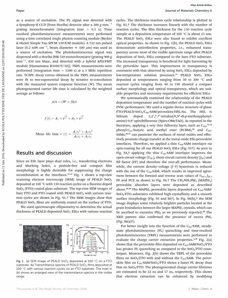
Since an ESL layer plays dual roles, i.e., transferring electronsand blocking holes, a pinhole-free and compact lmmorphology is highly desirable for suppressing the chargerecombination at the interfaces.51,52 Fig. 1 shows a top-viewscanning electron microscopy (SEM) image of PEALD SnO2
deposited at 100 �C with 130 reaction cycles on a uorine-dopedSnO2 (FTO) coated glass substrate. The top-view SEM images ofbare FTO and FTO coated with PEALD SnO2 with various reac-tion cycles are shown in Fig. S1.† The SEM images show thatPEALD SnO2 lms are uniformly coated on the surface of FTO.
We used spectroscopic ellipsometry to determine the actualthickness of PEALD deposited SnO2 ESLs with various reaction
Fig. 1 (a) SEM image of PEALD SnO2 deposited at 100 �C on a FTOsubstrate. (b) Transmittance spectra of PEALD SnO2 films deposited at100 �C with various reaction cycles on an FTO substrate. The inset in(b) shows an enlarged view of the transmittance spectra in the visiblerange.
This journal is © The Royal Society of Chemistry 2016
cycles. The thickness–reaction cycle relationship is plotted inFig. S2.† The thickness increases linearly with the number ofreaction cycles. The lm thickness for the 130 reaction cyclesample at a deposition temperature of 100 �C is about 15 nm.The PEALD SnO2 ESLs were also found to exhibit excellentoptical properties. As shown in Fig. 1(b), the PEALD SnO2 ESLsdemonstrate antireection properties, i.e., enhanced trans-parency across most of the visible spectrum range aer PEALDdeposition of SnO2 ESLs compared to the bare FTO substrate.The increased transparency is benecial for light harvesting bythe perovskite layer. This improvement in transparency isconsistent with that observed by using SnO2 ESLs deposited bylow-temperature solution processes.33 PEALD SnO2 ESLsdeposited at temperatures ranging from 50 to 200 �C andreaction cycles ranging from 40 to 190 showed a compactsurface morphology and optical transparency, which are suit-able properties and necessary requirements for efficient ESLs.
We systematically examined the relationship of the PEALDdeposition temperature and the number of reaction cycles withPVSC performance. We used a regular device structure of glass/FTO/PEALD-SnO2/C60-SAM/perovskite/HSL/Au. The HSL islithium doped 2,20,7,70-tetrakis(N,N0-di-p-methoxyphenyl-amine)-9,90-spirobiuorene (Spiro-OMeTAD). As reported in theliterature, applying a very thin fullerene layer, such as C60,51,52
phenyl-C61-butyric acid methyl ester (PCBM),48 and C60-SAMs,29,47 can passivate the surfaces of metal oxides and effec-tively promote charge transfer at the metal oxide ESL/perovskiteinterfaces. Therefore, we applied a thin C60-SAM interlayer viaspin-coating for all our PEALD SnO2 ESLs (Fig. S3†). As seen inFig. S4,† applying the thin C60-SAM interlayer improves theopen-circuit voltage (VOC), short-circuit current density (JSC) andll factor (FF) and therefore the over-all performance. Mean-while, the current density–voltage (J–V) hysteresis is reducedwith the use of the C60-SAM, which results in improved agree-ment between the forward and reverse scan values of VOC, JSC,FF and PCE as shown in Fig. S4.† The CH3NH3PbI3 (MAPbI3)perovskite absorber layers were deposited as describedabove.48,50 The MAPbI3 perovskite layers deposited on C60-SAM/SnO2/FTO substrates exhibited high crystallinity and a smoothsurface morphology (Fig. S5 and S6†). In Fig. S6(b),† the SEMimage displays some relatively brighter particles located at thegrain boundaries between the larger MAPbI3 crystals, which canbe ascribed to excessive PbI2 as we previously reported.48 TheXRD pattern also conrmed the presence of excess PbI2(Fig. S6(a)†).
For better insight into the function of the C60-SAM, steady-state photoluminescence (PL) quenching and time-resolvedphotoluminescence (TRPL) measurements were performed toevaluate the charge carrier extraction properties.3,30 Fig. 2(a)shows that the perovskite lm deposited on C60-SAM/SnO2/FTOhas greater PL quenching as compared to the SnO2/FTO coun-terpart. Moreover, Fig. 2(b) shows the TRPL of the perovskitelms on SnO2/FTO with and without the C60-SAM. The perov-skite lm on C60-SAM/SnO2/FTO shows a faster PL decay thanthat on SnO2/FTO. The photogenerated charge carrier lifetimesare estimated to be 22 ns and 57 ns, respectively. This showsthat electron extraction can be enhanced by modifying
J. Mater. Chem. A
Fig. 2 (a) Steady-state photoluminescence spectra and (b) photo-luminescence decay of perovskite films on C60-SAM/SnO2/FTO andSnO2/FTO substrates. (c) Impedance spectra and (d) J–V curves ofPVSCs based on C60-SAM/SnO2/FTO and SnO2/FTO substrates.
Fig. 3 Histogram of average (a) VOC, (b) JSC, (c) FF, and (d) PCE ofPVSCs using the PEALD SnO2 ESL deposited with various reactioncycles at 100 �C deposition temperature. Error bars represent thestandard deviation calculated for 54 devices prepared under the sameconditions.
Journal of Materials Chemistry A Paper
Publ
ishe
d on
11
July
201
6. D
ownl
oade
d by
EC
OL
E P
OL
YT
EC
HN
IC F
ED
DE
LA
USA
NN
E o
n 22
/07/
2016
09:
28:4
8.
View Article Online
perovskite/SnO2 contact with the C60-SAM. Impedance spec-troscopy (IS) was used to investigate interface charge transportand recombination in our PVSCs.20,21,33 Fig. 2(c) shows theNyquist plots of PVSCs employing C60-SAM/SnO2/FTO andSnO2/FTO as ESLs. The semicircle in the low frequency rangecan be attributed to the recombination resistance (Rrec) at theinterface of the perovskite and ESL. It is obvious that the Rrec issignicantly decreased aer C60-SAM passivation, indicatingreduced recombination. Furthermore, the semicircle in thehigh frequency range can be attributed to the transfer resistance(Rtr) at the perovskite/ESL interface. A lower Rtr was obtained inthe presence of the C60-SAM, manifesting faster charge transferat the optimized perovskite/ESL interface and favorable trans-port of photogenerated generated electrons. The larger Rrec andlower Rtr should lead to a higher VOC and FF, which is consistentwith our J–V results in Fig. 2(d). The VOC, JSC, FF and PCE ofPVSCs based on C60-SAM/SnO2/FTO are 1.126 V, 21.35 mA cm�2,79.10% and 19.02%, while those of PVSCs based on SnO2/FTOare 1.074 V 21.17 mA cm�2, 75.48% and 17.16%, respectively.The higher VOC and FF are ascribed to efficient electronextraction and hole blocking of the C60-SAM.
We rst explored the performance dependence on reactioncycles of 40, 70, 100, 130, 160, and 190; all with the depositiontemperature at 100 �C. Their corresponding thicknesses can befound in Fig. S2.† The J–V curves of some representative PVSCsusing PEALD SnO2 ESLs with various reaction cycles, measuredunder both reverse and forward voltage scans with a scan speedof 1 V s�1, are shown in Fig. S7.† The average device perfor-mance parameters including VOC, JSC, FF, and PCE for over 50cells are summarized in Table S1.† The histograms of theperformance parameters are shown in Fig. 3. It is noted thateven with a 40 reaction cycle PEALD SnO2 ESL (only a fewmonolayers thickness), the device showed an average VOChigher than 1.0 V. This is ascribed to the complete coverage andthe hole-blocking effect of the SnO2 ESL, as well as the passiv-ation effect of the C60-SAM. As the number of reaction cycles
J. Mater. Chem. A
increases, all performance parameters rst increase and thendecrease. The average PCE reaches the maximum with 130reaction cycles, which is about 15 nm as determined by spec-troscopic ellipsometry. This trend may be understood by thetrade-off between the electron transport properties and thehole-blocking ability of SnO2 ESLs. For increased hole-blocking,thicker SnO2 ESLs are preferred; however, for improved electrontransport, thinner SnO2 ESLs are required. Consequently, weselected PEALD SnO2 with 130 reaction cycles (15 nm) toinvestigate the effect of deposition temperature.
With the number of reaction cycles xed at 130, we thenvaried the deposition temperature for PEALD SnO2 ESLs: 50, 70,100, 150, and 200 �C. A large number of PVSCs using these SnO2
ESLs were fabricated. The J–V curves of some representativePVSCs measured under reverse and forward voltage scans areshown in Fig. S8.† The average device performance parametersof over 40 cells are summarized in Table S2† and their histo-grams are shown in Fig. 4. It is seen that the average VOC and FFrst increase and then decrease as the deposition temperatureincreases. The JSC appears to increase slightly as the depositiontemperature increases, although the change is almost withinthe order of the statistical variation. The average PCE reachesthe maximum value at 100 �C. This is about 20 �C lower than theprocessing temperature as reported for ozone ALD SnO2 ESLs.38
It is worth highlighting that even the SnO2 ESL deposited at 70�C can produce PVSCs with average efficiency close to 16%. Ifthe processing temperature is further decreased to 50 �C, thedevice performance decreased dramatically. It is likely that sucha low temperature cannot allow the metal precursors to fullyreact to form high-quality SnO2 ESLs, even in the presence ofplasma-generated reactive species. However, if the processingtemperature is too high, the SnO2 ESLs start to recrystallize,creating pinholes and a rough surface40 as shown in Fig. S9,†leading to decreased performance.
This journal is © The Royal Society of Chemistry 2016
Fig. 4 Histogram of average (a) VOC, (b) JSC, (c) FF, and (d) PCE ofPVSCs using the PEALD SnO2 ESL deposited at various processingtemperatures. Error bars represent the standard deviation calculatedfor 45 devices prepared under the same conditions.
Fig. 5 Hysteresis and stability of a representative PVSC. (a) J–V curvesof the perovskite devicemeasured under reverse voltage scan andwithdifferent scan speeds. (b) EQE spectrum and the integrated JSC plot. (c)J–V curves measured under reverse and forward voltage scans witha sweep speed of 1 V s�1. (d) Steady-state JSC and PCE of the devicewith a PEALD SnO2 ESL at a constant bias of 0.918 V under 100 mWcm�2 illumination. (e) Dependence of photovoltaic parameters on thetime, and (f) J–V curves measured under reverse voltage scan withtime under low humidity conditions.
Paper Journal of Materials Chemistry A
Publ
ishe
d on
11
July
201
6. D
ownl
oade
d by
EC
OL
E P
OL
YT
EC
HN
IC F
ED
DE
LA
USA
NN
E o
n 22
/07/
2016
09:
28:4
8.
View Article Online
The PVSCs using PEALD SnO2 ESLs deposited at 100 �C with130 reaction cycles have achieved an averaged efficiency of 18.21� 0.59%, with a JSC of 21.08 � 0.42 mA cm�2, a VOC of 1.11 �0.02 V and a FF of 77.62 � 1.34%. Our PVSCs exhibited verysmall J–V hysteretic behaviour. Fig. 5(a) shows J–V curves ofa PVSC using a PEALD SnO2 ESL deposited at 100 �C and with130 reaction cycles measured under reverse voltage scan withvarious scan rates. The results indicate that the performance ofour devices is relatively independent of the scan rate. The JSC(21.50 mA cm�2) from the J–V curves is very close to the inte-grated photocurrent (21.20 mA cm�2) from the externalquantum efficiency (EQE) as shown in Fig. 5(b). The J–V curvesof this PVSC measured under both reverse and forward voltagescan directions are shown in Fig. 5(c), showing almost nohysteresis. The VOC, JSC, FF, and PCE are 1.08 (1.07) V, 21.80(21.81) mA cm�2, 76.95 (75.48)%, and 18.12 (17.61)%, respec-tively, whenmeasured under reverse (forward) voltage scan. Thecorresponding steady-state efficiency is 17.55%, as shown inFig. 5(d). The current density is 19.12 mA cm�2 and the effi-ciency is 17.55% under a bias of 0.918 V, which is very close to J–V extracted efficiency. It is encouraging that this PVSC alsoshowed good stability when kept under N2 conditions withrelative humidity below 10% and under normal room light. Theoutput power remained unaltered with the storage time, asshown in Fig. 5(e). Aer being stored for 480 hours, the VOCincreased from 1.09 V to 1.11 V, while the FF decreased slightlyand the JSC remained unchanged, leading to a negligible changeof the PCE. The J–V curves of this PVSC measured under reversevoltage scan aer various storage times almost overlapped(Fig. 5(f)). The good stability of PVSCs with the PEALD SnO2 ESLmight be attributable to the negligible catalytic character ofSnO2 and its relative insensitivity to ultraviolet (UV) light (muchlower than PVSCs fabricated with TiO2 (ref. 53 and 54)), whichmay lead to the negligible degradation of photocurrentobserved in our devices.
This journal is © The Royal Society of Chemistry 2016
The low-temperature deposition of efficient SnO2 ESLsenabled by PEALD is particularly benecial for fabricatingexible PVSCs. We have fabricated exible PVSCs on indium-doped SnO2 (ITO)/polyethylene terephthalate (PET) substrates.The PEALD SnO2 ESLs were deposited at 100 �C with 130 reac-tion cycles. Over 30 exible PVSCs were fabricated, and theiraverage VOC, JSC, FF, and PCE are 1.07 � 0.04 (1.03 � 0.05) V,20.68 � 0.22 (20.74 � 0.28) mA cm�2, 70.33 � 3.18 (61.70 �3.42)%, and 15.57 � 1.14 (13.18 � 1.00)%, respectively, whenmeasured under reverse (forward) voltage scan. The J–V curvesmeasured under both reverse and forward voltage scans and theEQE spectra of the best-performing PVSC on FTO/glass and ITO/PET substrates are shown in Fig. 5(a) and (b), respectively. Thebest-performing PVSC fabricated on FTO/glass showed a PCE of19.03 (18.24)% with a VOC of 1.13 (1.10) V, a JSC of 21.56 (21.55)mA cm�2, and a FF of 78.11 (76.93)% under reverse (forward)scan. Meanwhile, the best-performing exible PVSC showeda PCE of 16.80 (15.48)% with a VOC of 1.11 (1.09) V, a JSC of 20.50(20.50) mA cm�2, and a FF of 73.82 (69.28)% under reverse(forward) voltage scan. J–V curves of one exible PVSCmeasuredunder reverse and forward voltage scans with various scan ratesare shown in Fig. S10.† Current densities integrated from theEQE spectra are shown in Fig. 6(b), which are 21.14 and 19.61mA cm�2 for the best cells fabricated on FTO/glass and exible
J. Mater. Chem. A
Fig. 7 Light intensity dependence of flexible devices under differentillumination.
Journal of Materials Chemistry A Paper
Publ
ishe
d on
11
July
201
6. D
ownl
oade
d by
EC
OL
E P
OL
YT
EC
HN
IC F
ED
DE
LA
USA
NN
E o
n 22
/07/
2016
09:
28:4
8.
View Article Online
ITO/PET substrates, respectively. They are in good agreementwith those from the J–V curves. It is noteworthy to point out thatthe VOC of the best exible PVSC is 1.11 V, only 20mV lower thanthat of the best PVSC on the FTO substrate, implying thata pinhole-free and compact SnO2 ESL also forms on the ITO/PET surface, leading to effective hole-blocking and minimizedcharge recombination. The absorbance spectra of MAPbI3deposited on two substrates, shown in Fig. 6(c), reveal theidentical onsets at about 778 nm, indicating similar absorptioncharacteristics irrespective of the substrates (XRD and SEMinformation of perovskite lms deposited on the ITO/PETsubstrates is provided in Fig. S11†). The lower FF of the exibledevice is likely attributable to the relatively higher sheet resis-tance of the ITO on exible PET (�45 U ,�1), compared withthe high-temperature processed FTO electrode on glass (�15 U
,�1). The tapping-mode atomic-force microscopy (AFM)images of FTO and ITO shown in Fig. S12† reveal that the FTOalso has much larger grain sizes than the ITO. We have alsomeasured the effect of bending fatigue cycles on the deviceperformance as shown in Fig. 6(d). Aer 200 times of bendingwith a minimum radius of curvature of 5 mm, the PCE is still14.00%, approximately 85% of its initial PCE of 16.50%, indi-cating good exibility endurance of our PVSCs with the low-temperature PEALD SnO2 ESL. The signicant change of theexible device performance upon multiple bending originatesfrom the decreased FF, from its initial 71.35 to 61.65% aer 200times of bending. As shown in Fig. 6(d), the FF decreaseddramatically with bending cycles, which can also be observed inthe J–V curves in Fig. S13(b).† This change is likely ascribable tothe increase in the sheet resistance of the ITO/PET exiblesubstrate, and thus the series resistance of the PVSC, as shownin Fig. S13(a) and (c),† respectively. The increase in the sheetresistance of the ITO/PET substrate with bending time is one ofthe main causes for the decreased FF. The inset of Fig. 6(d)
Fig. 6 The best-performing devices based on PEALD SnO2 coatedFTO/glass and ITO/PET substrates: (a) J–V curves under reverse andforward voltage scans. (b) EQE spectra and their corresponding inte-grated photocurrents. (c) Absorption spectra of perovskite films. (d)Normalized performance parameters of a flexible PVSC versusbending cycles. Photograph of a flexible device after the bending test(inset).
J. Mater. Chem. A
shows a photograph of our exible device aer the bending test,which still has a shiny and smooth surface without anyobservable damage.
To further understand the charge recombination mecha-nism in the exible devices, light intensity dependencemeasurements were carried out under different light intensitiesranging from 0.5 to 100 mW cm�2 as shown in Fig. 7. Fig. 7(a)shows the corresponding J–V curves under the different illu-mination intensities. The power law dependence of JSC on lightintensity (J–Ia) is shown in Fig. 7(b). A solar device with spacecharge effects will have a factor a ¼ 0.75 while if a is close to 1,there is no space charge.55 This exible device shows a value ofa ¼ 0.952, indicating a negligible space charge effect. The VOChas a linear relationship with logarithmic light intensity asshown in Fig. 7(c), indicating the presence of Shockley–Read–Hall recombination in the exible device. Fig. 7(d) displays thedependence of FF on light intensity. Our device congurationon a exible substrate produces a marginal FF dependence onlight intensity, with a maximum FF of 77.50% obtained under20 mW cm�2 illumination, indicating minimized chargerecombination at relatively lower light intensity. These resultssuggest that our exible device has a low charge recombinationrate with no obvious interfacial energy barrier.
Conclusions
We have demonstrated that the PEALD technique could reducethe effective deposition temperature of SnO2 ESLs to less than100 �C without compromising the PVSC performance. Aerpassivating the surface of SnO2 ESLs with a C60-SAM, the bestPVSCs fabricated on glass substrates have achieved averagePCEs and steady-state efficiencies above 18%. The SnO2 ESLsdeposited by PEALD at 70 �C enabled the fabrication of PVSCswith average PCEs higher than 17%. Furthermore, the bestexible PVSCs with PEALD SnO2 ESLs deposited at 100 �C haveachieved 16.80% PCE, with an average PCE higher than 15%.
This journal is © The Royal Society of Chemistry 2016
Paper Journal of Materials Chemistry A
Publ
ishe
d on
11
July
201
6. D
ownl
oade
d by
EC
OL
E P
OL
YT
EC
HN
IC F
ED
DE
LA
USA
NN
E o
n 22
/07/
2016
09:
28:4
8.
View Article Online
Therefore, our results demonstrate the potential of PEALD forsynthesizing high quality SnO2 ESLs at very low temperature forfabricating highly efficient perovskite solar cells.
Acknowledgements
This work is nancially supported by the U.S. Department ofEnergy (DOE) SunShot Initiative under the Next GenerationPhotovoltaics 3 program (DE-FOA-0000990), National ScienceFoundation under contract no. CHE-1230246 and DMR-1534686, and the Ohio Research Scholar Program. The work atthe National Renewable Energy Laboratory was supported bythe U.S. Department of Energy SunShot Initiative under the NextGeneration Photovoltaics 3 program (DE-FOA-0000990) underContract No. DE-AC36-08-GO28308. This research used theresources of the Ohio Supercomputer Center and the NationalEnergy Research Scientic Computing Center, which is sup-ported by the Office of Science of the U.S. Department of Energyunder Contract No. DE-AC02-05CH11231. This work alsoreceived nancial support from the National Basic ResearchProgram of China (2011CB933300), National Science Fund forDistinguished Young Scholars (50125309), and National NaturalScience Foundation of China (Grants 51272184 and 91433203).
Notes and references
1 A. Kojima, K. Teshima, Y. Shirai and T. Miyasaka, J. Am.Chem. Soc., 2009, 131, 6050–6051.
2 W. S. Yang, J. H. Noh, N. J. Jeon, Y. C. Kim, S. Ryu, J. Seo andS. I. Seok, Science, 2015, 348, 1234–1237.
3 D. Bi, W. Tress, M. I. Dar, P. Gao, J. Luo, C. Renevier,K. Schenk, A. Abate, F. Giordano and J.-P. C. Baena, Sci.Adv., 2016, 2, e1501170.
4 N. J. Jeon, J. H. Noh, W. S. Yang, Y. C. Kim, S. Ryu, J. Seo andS. I. Seok, Nature, 2015, 517, 476–480.
5 J.-H. Im, C.-R. Lee, J.-W. Lee, S.-W. Park and N.-G. Park,Nanoscale, 2011, 3, 4088–4093.
6 M. M. Lee, J. Teuscher, T. Miyasaka, T. N. Murakami andH. J. Snaith, Science, 2012, 338, 643–647.
7 S. D. Stranks, G. E. Eperon, G. Grancini, C. Menelaou,M. J. Alcocer, T. Leijtens, L. M. Herz, A. Petrozza andH. J. Snaith, Science, 2013, 342, 341–344.
8 W. J. Yin, H. Chen, T. Shi, S. H. Wei and Y. Yan, Adv. Electron.Mater., 2015, 1, 1500044.
9 W. J. Yin, T. Shi and Y. Yan, Adv. Mater., 2014, 26, 4653–4658.10 W.-J. Yin, T. Shi and Y. Yan, Appl. Phys. Lett., 2014, 104,
063903.11 W.-J. Yin, T. Shi and Y. Yan, J. Phys. Chem. C, 2015, 119,
5253–5264.12 M. L. Agiorgousis, Y.-Y. Sun, H. Zeng and S. Zhang, J. Am.
Chem. Soc., 2014, 136, 14570–14575.13 M.-H. Du, J. Phys. Chem. Lett., 2015, 6, 1461–1466.14 J. Burschka, N. Pellet, S.-J. Moon, R. Humphry-Baker, P. Gao,
M. K. Nazeeruddin and M. Gratzel, Nature, 2013, 499, 316–319.
15 J.-H. Im, I.-H. Jang, N. Pellet, M. Gratzel and N.-G. Park, Nat.Nanotechnol., 2014, 9, 927–932.
This journal is © The Royal Society of Chemistry 2016
16 A. Mei, X. Li, L. Liu, Z. Ku, T. Liu, Y. Rong, M. Xu, M. Hu,J. Chen and Y. Yang, Science, 2014, 345, 295–298.
17 N. Ahn, D.-Y. Son, I.-H. Jang, S. M. Kang, M. Choi andN.-G. Park, J. Am. Chem. Soc., 2015, 137, 8696–8699.
18 D. Zhao, M. Sexton, H. Y. Park, G. Baure, J. C. Nino and F. So,Adv. Energy Mater., 2015, 5, 1401855.
19 N. Cheng, P. Liu, S. Bai, Z. Yu, W. Liu, S.-S. Guo andX.-Z. Zhao, J. Power Sources, 2016, 319, 111–115.
20 Z. Yu, F. Qi, P. Liu, S. You, K. K. Kondamareddy, C. Wang,N. Cheng, S. Bai, W. Liu, S. Guo and X.-z. Zhao, Nanoscale,2016, 8, 5847–5851.
21 Z. Yu, B. Chen, P. Liu, C. Wang, C. Bu, N. Cheng, S. Bai,Y. Yan and X. Zhao, Adv. Funct. Mater., 2016, DOI: 10.1002/adfm.201504564.
22 G. Xing, N. Mathews, S. Sun, S. S. Lim, Y. M. Lam, M. Gratzel,S. Mhaisalkar and T. C. Sum, Science, 2013, 342, 344–347.
23 M. Liu, M. B. Johnston and H. J. Snaith, Nature, 2013, 501,395–398.
24 J. H. Heo, H. J. Han, D. Kim, T. K. Ahn and S. H. Im, EnergyEnviron. Sci., 2015, 8, 1602–1608.
25 C. Wang, Z. Yu, C. Bu, P. Liu, S. Bai, C. Liu,K. K. Kondamareddy, W. Sun, K. Zhan, K. Zhang, S. Guoand X. Zhao, J. Power Sources, 2015, 282, 596–601.
26 L. Zuo, Z. Gu, T. Ye, W. Fu, G. Wu, H. Li and H. Chen, J. Am.Chem. Soc., 2015, 137, 2674–2679.
27 J. You, L. Meng, T.-B. Song, T.-F. Guo, Y. M. Yang,W.-H. Chang, Z. Hong, H. Chen, H. Zhou and Q. Chen,Nat. Nanotechnol., 2016, 11, 75–81.
28 J. Song, E. Zheng, J. Bian, X.-F. Wang, W. Tian, Y. Sanehiraand T. Miyasaka, J. Mater. Chem. A, 2015, 3, 10837–10844.
29 X. Liu, K. W. Tsai, Z. Zhu, Y. Sun, C. C. Chueh andA. K. Y. Jen, Adv. Mater. Interfaces, 2016, DOI: 10.1002/admi.201600122.
30 H. S. Rao, B. X. Chen, W. G. Li, Y. F. Xu, H. Y. Chen,D. B. Kuang and C. Y. Su, Adv. Funct. Mater., 2015, 25,7200–7207.
31 Z. Zhu, Y. Bai, X. Liu, C. C. Chueh, S. Yang and A. K. Y. Jen,Adv. Mater., 2016, DOI: 10.1002/adma.201600619.
32 T. P. Chou, Q. Zhang and G. Cao, J. Phys. Chem. C, 2007, 111,18804–18811.
33 W. Ke, G. Fang, Q. Liu, L. Xiong, P. Qin, H. Tao, J. Wang,H. Lei, B. Li and J. Wan, J. Am. Chem. Soc., 2015, 137,6730–6733.
34 Q. Dong, Y. Shi, K. Wang, Y. Li, S. Wang, H. Zhang, Y. Xing,Y. Du, X. Bai and T. Ma, J. Phys. Chem. C, 2015, 119, 10212–10217.
35 S. S. Shin, W. S. Yang, J. H. Noh, J. H. Suk, N. J. Jeon,J. H. Park, J. S. Kim, W. M. Seong and S. I. Seok, Nat.Commun., 2015, 6, 7140.
36 J. Yang, B. D. Siempelkamp, E. Mosconi, F. De Angelis andT. L. Kelly, Chem. Mater., 2015, 27, 4229–4236.
37 Q. Hu, J. Wu, C. Jiang, T. Liu, X. Que, R. Zhu and Q. Gong,ACS Nano, 2014, 8, 10161–10167.
38 J. P. C. Baena, L. Steier, W. Tress, M. Saliba, S. Neutzner,T. Matsui, F. Giordano, T. J. Jacobsson, A. R. S. Kandadaand S. M. Zakeeruddin, Energy Environ. Sci., 2015, 8, 2928–2934.
J. Mater. Chem. A
Journal of Materials Chemistry A Paper
Publ
ishe
d on
11
July
201
6. D
ownl
oade
d by
EC
OL
E P
OL
YT
EC
HN
IC F
ED
DE
LA
USA
NN
E o
n 22
/07/
2016
09:
28:4
8.
View Article Online
39 B. Selin Tosun, R. K. Feist, S. A. Campbell and E. S. Aydil, J.Vac. Sci. Technol., A, 2012, 30, 04D101.
40 X. Meng, Y. Zhang, S. Sun, R. Li and X. Sun, J. Mater. Chem.,2011, 21, 12321–12330.
41 D. Yang, R. Yang, J. Zhang, Z. Yang, S. F. Liu and C. Li, EnergyEnviron. Sci., 2015, 8, 3208–3214.
42 S. S. Shin, W.-S. Yang, E. J. Yeom, S. J. Lee, N. J. Jeon,Y.-C. Joo, J. H. Noh, S. I. Seok and I. J. Park, J. Phys. Chem.Lett., 2016, 7, 1845–1851.
43 D. Yang, R. Yang, X. Ren, X. Zhu, Z. Yang, C. Li and S. Liu,Adv. Mater., 2016, 28, 5206–5213.
44 H. B. Projt, S. E. Potts, M. C. M. van de Sanden andW. M. M. Kessels, J. Vac. Sci. Technol., A, 2011, 29, 050801.
45 S. E. Potts, W. Keuning, E. Langereis, G. Dingemans,M. C. M. van de Sanden and W. M. M. Kessels, J.Electrochem. Soc., 2010, 157, P66–P74.
46 C.-C. Chueh, C.-Z. Li and A. K.-Y. Jen, Energy Environ. Sci.,2015, 8, 1160–1189.
47 K. Wojciechowski, S. D. Stranks, A. Abate, G. Sadoughi,A. Sadhanala, N. Kopidakis, G. Rumbles, C.-Z. Li,R. H. Friend, A. K. Y. Jen and H. J. Snaith, ACS Nano, 2014,8, 12701–12709.
J. Mater. Chem. A
48 W. Ke, C. Xiao, C. Wang, B. Saparov, H.-S. Duan, D. Zhao,Z. Xiao, P. Schulz, S. P. Harvey, W. Liao, W. Meng, Y. Yu,A. J. Cimaroli, C.-S. Jiang, K. Zhu, M. Al-Jassim, G. Fang,D. B. Mitzi and Y. Yan, Adv. Mater., 2016, 28, 5214–5221.
49 Y. Chen, B. Li, W. Huang, D. Gao and Z. Liang, Chem.Commun., 2015, 51, 11997–11999.
50 M. Xiao, F. Huang, W. Huang, Y. Dkhissi, Y. Zhu,J. Etheridge, A. Gray-Weale, U. Bach, Y.-B. Cheng andL. Spiccia, Angew. Chem., 2014, 126, 10056–10061.
51 W. Ke, D. Zhao, C. R. Grice, A. J. Cimaroli, J. Ge, H. Tao,H. Lei, G. Fang and Y. Yan, J. Mater. Chem. A, 2015, 3,17971–17976.
52 D. Zhao, W. Ke, C. R. Grice, A. J. Cimaroli, X. Tan, M. Yang,R. W. Collins, H. Zhang, K. Zhu and Y. Yan, Nano Energy,2016, 19, 88–97.
53 T. Leijtens, G. E. Eperon, S. Pathak, A. Abate, M. M. Lee andH. J. Snaith, Nat. Commun., 2013, 4, 2885.
54 C.-H. Wu, Chemosphere, 2004, 57, 601–608.55 V. Mihailetchi, J. Wildeman and P. Blom, Phys. Rev. Lett.,
2005, 94, 126602.
This journal is © The Royal Society of Chemistry 2016