Embed Size (px)
Citation preview

FS-K350QVG-V2-F
21/Jul/2008
PAGE 1 OF 20
Kitronix (Dong guan) Ltd. PRODUCT SPECIFICATION
Product Standard LCD Module 320 x RGB x 240 Dots 3.5” 262K colors TFT display Wide temperature With white LED backlight With Touch Panel
K350QVG-V2-F
Kitronix (Dong Guan) Ltd.

FS-K350QVG-V2-F
21/Jul/2008
PAGE 2 OF 20
Kitronix (Dong guan) Ltd. PRODUCT SPECIFICATION
CONTENTS Page No. 1. DOCUMENT REVISION HISTORY 3 2. GENERAL DESCRIPTION 4 3. MECHANICAL SPECIFICATIONS 4 4. INTERFACE SIGNALS 6 5. ABSOLUTE MAXIMUM RATINGS 7 6. ELECTRICAL SPECIFICATIONS 7 7. OPTICAL CHARACTERISTICS 8 8. TIMING CHARACTERISTICS 10 9. RELIABILITY TEST ITEM 12 10. SUGGESTIONS FOR USING LCD MODULES 13 11. INSPECTION STANDARD 16 12. PACKING(REFERENCE ONLY) 22

FS-K350QVG-V2-F
21/Jul/2008
PAGE 3 OF 20
Kitronix (Dong guan) Ltd. PRODUCT SPECIFICATION
1. Document revision history : DOCUMENT
REVISION DATE DESCRIPTION PREPARED BY
APPROVED BY
01 2008.04.28 First Release. Van Ng

FS-K350QVG-V2-F
21/Jul/2008
PAGE 4 OF 20
Kitronix (Dong guan) Ltd. PRODUCT SPECIFICATION
2. General Description
• 3.5”(diagonal), 320 x RGB x 240 dots, 262K colors, Transmissive, TFT LCD module. • Viewing Direction: 12 o’clock. • Driving IC: SSD2119 or equivalent TFT controller/driver. • 18-bits data bus (parallel RGB interface/8080 parallel system interface). • With Touch Panel. • With internal voltage booster. • Logic voltage: 3.3V (typ.).
3. Mechanical Specifications The mechanical detail is shown in Fig. 1 and summarized in Table 1 below.
Table 1 Parameter Specifications Unit
Outline dimensions 76.9(W) x 63.9(H) x 4.4(D) (Exclude FPC, cables of backlight) mm
View area 72.88(W) x 55.36(H) mm TP view area 71.58 (W) x 54.2(H) mm
LCD active area 70.08(W) x 52.56(H) mm Display format 320 x RGB x 240 dots
Color configuration RGB stripes -
Color TFT 320xRGBx240
Dot size 0.219(RGB)(W) x 0.219(H) mm Weight TBD grams

FS-K350QVG-V2-F
21/Jul/2008
PAGE 5 OF 20
Kitronix (Dong guan) Ltd. PRODUCT SPECIFICATION
▽ 建议客户机壳开窗单边比TPVA单边小0.
3mm,机壳泡棉开窗比TPVA单边大0.6mm
▽
▽ ▽
▽
Figure 1: Outline Drawing

FS-K350QVG-V2-F
21/Jul/2008
PAGE 6 OF 20
Kitronix (Dong guan) Ltd. PRODUCT SPECIFICATION
4. Interface signals Table 2: Pin assignment
Pin No. Symbol Description 1-2 LED_K 3-4 LED_A
Power supply for LED backlight
5 GND Power supply (system ground) 6 XR 7 YD 8 XL 9 YU
Terminal of touch panel.
10 GND Power supply (system ground) 11-13 NC No connection
14 RESET System reset pin 15 CS Chip select pin 16 SPCLK Clock pin of serial interface 17 SDA-SDI Data pin of serial interface
18-19 NC No connection 20-25 B[0-5] Blue data 6-bit/18bit bi-directional (D0-D5) 26-27 NC No connection 28-33 G[0-5] Green data 6-bit/18bit bi-directional (D6-D11) 34-35 NC No connection 36-41 R[0-5] Red data 6-bit/18bit bi-directional (D12-D17)
42 HSYNC Line synchronization signal input 43 VSYNC Frame /Ram synchronization signal input 44 DCLK Dot clock signal
45-46 AVDD Supply voltage for lcd driving 47-48 VCC Supply voltage for logic
49 DC Parallel Interface 50 RD I80 system: Serves as a read signal and reads data at the low level. 51 WR I80 system: Serves as a write signal and writes data at the rising edge.
52-55 PS[0:3]
Interface selection pin PS3 PS2 PS1 PS0 Interface mode
0 0 1 0 16-bit 8080 parallel interface, D[17:10]&D[8:1] 0 0 1 1 8-bit 8080 parallel interface, D[8:1] 0 1 0 0 9-bit RGB(262 colour) + 3-wire SPI, D[8:0] 0 1 0 1 16-bit RGB(262K colour) + 3-wire SPI,
D[17:10]&D[8:1] 0 1 1 0 18-bit RGB(262K colour) + 3-wire SPI, D[17:0] 0 1 1 1 6-bit RGB(262K colour) + 3-wire SPI, D[8:3] 1 0 1 0 18-bit 8080 parallel interface, D[17:0] 1 0 1 1 9-bit 8080 parallel interface, D[8:0] 1 1 1 0 3-wire SPI
56 WSYNC Ram Write Synchronization output 57 NC No connection 58 OE Display enable pin from controller
59-60 GND Power supply (system ground)

FS-K350QVG-V2-F
21/Jul/2008
PAGE 7 OF 20
Kitronix (Dong guan) Ltd. PRODUCT SPECIFICATION
5. Absolute Maximum Ratings 5.1 Electrical Maximum Ratings – for IC Only
Table 3: Electrical Maximum Ratings – for IC Parameter Symbol Min. Max. Unit Note
Supply voltage VCC -0.3 +4.0 V 1 Input voltage AVDD -0.3 +5.0 V
Note: 1.VCC, GND must be maintained.
2.The modules may be destroyed if they are used beyond the absolute maximum ratings. 5.2 Environmental Condition
Table 4
Operating temperature
(Topr)
Storage temperature
(Tstg) (Note 1)
Item
Min. Max. Min. Max.
Remark
Ambient temperature -20°C +70°C -30°C +80°C Dry
Humidity (Note 1) 80% max. RH for Ta ≤ 40°C < 50% RH for 40°C < Ta ≤ Maximum operating temperature
No condensation
Note 1: Product cannot sustain at extreme storage conditions for long time. 6. Electrical Specifications
Typical Electrical Characteristics At Ta = 25 °C, VCC=IOVCC= 3.3V, GND=0V.
Table 5 Parameter Symbol Conditions Min. Typ. Max. Unit
Supply voltage (logic) VCC-GND 1.4 - 3.6 V
Supply voltage (lcd driving) AVDD 2.5 or VDDIO - 3.6 V
VGH 9 - 18.0 V VGL -15.0 - -6 V Output voltage(LCD)
VCOM -1 - 6 V Supply current (Logic & LCD) ICC VDD=2.2V - - 10 mA
Supply voltage of white LED backlight VLED - 19.2 21.6 V
Luminance (on the module surface)
Forward current =20 mA
Number of LED dies = 6 230 270 - cd/m2

FS-K350QVG-V2-F
21/Jul/2008
PAGE 8 OF 20
Kitronix (Dong guan) Ltd. PRODUCT SPECIFICATION
7. Optical Characteristics Table 7: Optical specifications
Specifications Items Symbol Condition Min. Typ. Max.
Unit
Contrast Ratio CR 150 300 - - TR - 15 30 ms Response Time TF - 35 50 ms XR 0.604 0.624 0.644 - Red YR 0.302 0.322 0.342 - XG 0.268 0.288 0.308 - Green YG 0.540 0.560 0.580 - XB 0.127 0.147 0.167 - Blue YB 0.097 0.117 0.137 - XW - 0.307 - -
Chromaticity
White YW
- 0.328 - - φ1(3 o’clock) - 45 - Hor. φ2(9 o’clock) - 45 -
θ2(12 o’clock) - 15 - Viewing angle
Ver. θ1(6 o’clock)
Center CR=10
- 35 -
deg.
NTSC ratio 61.5 %
Note
Note 1: Definition of Contrast Ratio (CR): The contrast ratio can be calculated by the following expression. Contrast Ratio (CR) = L63 / L0 L63: Luminance of gray level 63 L0: Luminance of gray level 0 CR = CR (10) CR (X) is corresponding to the Contrast Ratio of the point X at Figure in Note 5. Note 2: Definition of Response Time (TR, TF):
Figure 3

FS-K350QVG-V2-F
21/Jul/2008
PAGE 9 OF 20
Kitronix (Dong guan) Ltd. PRODUCT SPECIFICATION
Note 3: Viewing Angle
Figure 4
The above “Viewing Angle” is the measuring position with Largest Contrast Ratio; not for good
image quality. View Direction for good image quality is 6 O’clock. Module maker can increase
the “Viewing Angle” by applying Wide View Film.
Note 4: Measurement Set-Up:
The LCD module should be stabilized at a given temperature for 20 minutes to avoid abrupt temperature change during measuring. In order to stabilize the luminance, the measurement should be executed after lighting Backlight for 20 minutes in a windless room.
Figure 5

FS-K350QVG-V2-F
21/Jul/2008
PAGE 10 OF 20
Kitronix (Dong guan) Ltd. PRODUCT SPECIFICATION
8. AC Characteristics 8.1 Parallel 8080 Timing Characteristics
Please refer SSD2119 datasheet. 9. Reliability Test Item
Test Item Sample Type Test Condition Test result determinant gist
Normal temperature 70±3℃;96H High temperature storage Wide temperature 80±3 ;℃ 96H
Normal temperature -20±3 ;℃ 120H Low temperature storage Wide temperature -30±3 ;℃ 120H
Normal temperature 50 ±3 ,90%±3%RH;℃ ℃ 96H High temperature /humidity storage Wide temperature 60 ±3 ,90%±3%RH;℃ ℃ 96H
the inspection of appearance and function
character.
Normal temperature 60±3 ;96H℃ High temperature operation Wide temperature 70±3 ;96H℃
Normal temperature 0±3 ;96H℃ Low temperature operation Wide temperature -20±3 ;96H℃
Normal temperature 40 ±3 ,90%±3%RH;96H℃ ℃ High temperature /humidity operation Wide temperature 50 ±3 ,90%±3%RH;96H℃ ℃
no objection of the function character; no fatal objection of
the appearance.
Normal temperature -20±3℃,30min? 70±3℃,30min;10cycle
inspect the objections appearance、function & the
whole structure
Temperature Shock
Wide temperature -30±3℃,30min 80±3,30min;10cycle
The inspection of appearance、function & the whole structure

FS-K350QVG-V2-F
21/Jul/2008
PAGE 11 OF 20
Kitronix (Dong guan) Ltd. PRODUCT SPECIFICATION
10. Suggestions for using LCD modules
10.1 Handling of LCM
1. The LCD screen is made of glass. Don't give excessive external shock, or drop from a high place.
2. If the LCD screen is damaged and the liquid crystal leaks out, do not lick and swallow. When the liquid
is attach to your hand, skin, cloth etc, wash it off by using soap and water thoroughly and immediately.
3. Don't apply excessive force on the surface of the LCM.
4. If the surface is contaminated ,clean it with soft cloth. If the LCM is severely contaminated , use
Isopropyl alcohol/Ethyl alcohol to clean. Other solvents may damage the polarizer . The following
solvents is especially prohibited: water , ketone Aromatic solvents etc.
5. Exercise care to minimize corrosion of the electrode. Corrosion of the electrodes is accelerated by
water droplets, moisture condensation or a current flow in a high-humidity environment.
6. Install the LCD Module by using the mounting holes. When mounting the LCD module make sure it is
free of twisting, warping and distortion. In particular, do not forcibly pull or bend the I/O cable or the
backlight cable.
7. Don’t disassemble the LCM.
8. To prevent destruction of the elements by static electricity, be careful to maintain an optimum work
environment.
- Be sure to ground the body when handling the LCD modules.
- Tools required for assembling, such as soldering irons, must be properly grounded.
- To reduce the amount of static electricity generated, do not conduct assembling and other work
under dry conditions.
- The LCD module is coated with a film to protect the display surface. Exercise care when peeling
off this protective film since static electricity may be generated.
9. Do not alter, modify or change the the shape of the tab on the metal frame.
10. Do not make extra holes on the printed circuit board, modify its shape or change the positions of
components to be attached.

FS-K350QVG-V2-F
21/Jul/2008
PAGE 12 OF 20
Kitronix (Dong guan) Ltd. PRODUCT SPECIFICATION
11. Do not damage or modify the pattern writing on the printed circuit board.
12. Absolutely do not modify the zebra rubber strip (conductive rubber) or heat seal connector
13. Except for soldering the interface, do not make any alterations or modifications with a soldering iron.
14. Do not drop, bend or twist LCM.
10.2 Cautions for installing and assemabling if the module has Touch Panel
1. Use a buffer material (Gasket) between the touch panel and Front-case to protect damage and wrong
operating. The dimension of the buffer material’s edge between the TP V.A. edge is Min. 0.3mm.
2. We recommend to design a case that it can’t over the boundary of the active area Max. 0.5mm in order
to prevent an operation at outside of the active area which can’t guarantee the specified durability,
because operation at the outside of the active area cause serious damage of a transparent.
3. When design case for installing Module, you would consider give a distance about 0.2±0.15mm
between the module edge to case inside.
4. The corners of the product are not chamfered. When positioning and fixing the product on the case, we
sugguest that you would provide a R part on the conner of the case so as not to apply load on the corner
of the transparent module.
驱动区域边缘
可视区域边缘
背光
绝缘油墨区域
缓冲材料 垫圈
机壳
触摸屏
FS-K350QVG-V2-F
21/Jul/2008
PAGE 13 OF 20
Kitronix (Dong guan) Ltd. PRODUCT SPECIFICATION
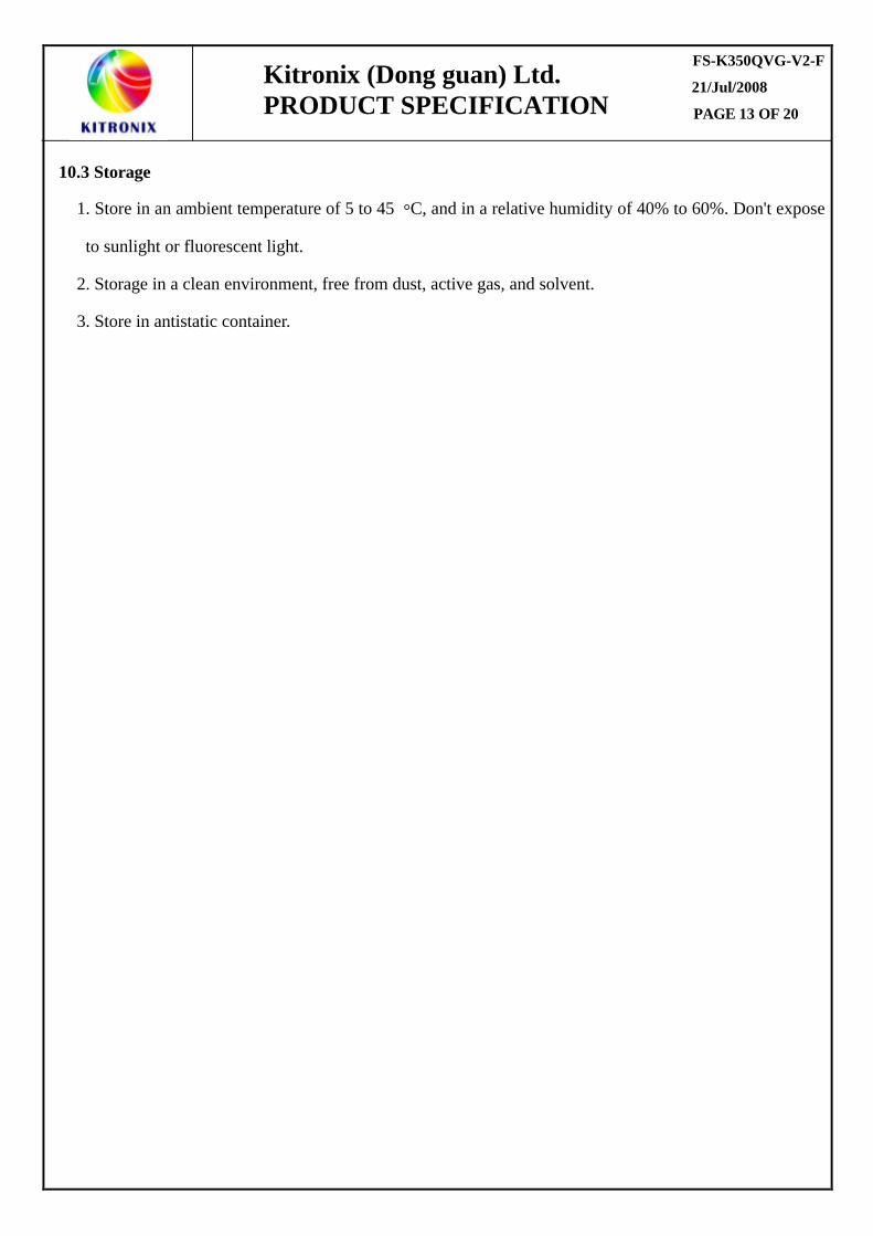
10.3 Storage
1. Store in an ambient temperature of 5 to 45 °C, and in a relative humidity of 40% to 60%. Don't expose
to sunlight or fluorescent light.
2. Storage in a clean environment, free from dust, active gas, and solvent.
3. Store in antistatic container.

FS-K350QVG-V2-F
21/Jul/2008
PAGE 14 OF 20
Kitronix (Dong guan) Ltd. PRODUCT SPECIFICATION
11. Inspection Standard This specification is made to be used as the standard acceptance/rejection criteria for Color mobile phone
LCM with touch pannel. 11.1 Sample plan and Inspection condition 11.1.1 Sample plan Sampling plan according to MIL-STD-105E , normal level 2 and based on: Major defect: AQL 0.65; Minor defect: AQL 1.5. 11.1.2 Inspection condition Viewing distance for cosmetic inspection is about 30cm with bare eyes, and under an environment of
20~40W light intensity, all directions for inspecting the sample should be within 45 against perpendicular line.
11.2 Definition of inspection zone in LCD
Inspection zones in an LCD
Zone A: character/Digit area; Zone B: viewing area except Zone A (ZoneA+ZoneB=minimum Viewing area); Zone C: Outside viewing area (invisible area after assembly in customer’s product); Note: As a general rule, visual defects in Zone C are permissible, when it is no trouble for quality and
assembly of customer’s product. Defects are classified as major defects and minor defects according to the degree of defectiveness defined herein.
11.3 Major defects and Minor defects 11.3.1 Major defects
A major defect is a defect that is likely to result in failure, or to reduce the usability of the product for its intended purpose. 11.3.1.1 Abnormal operation: modules cannot display normally;

FS-K350QVG-V2-F
21/Jul/2008
PAGE 15 OF 20
Kitronix (Dong guan) Ltd. PRODUCT SPECIFICATION
11.3.1.2 Line defect; 11.3.1.3 There is serious distortion or sharp burr on mechanical housing; 11.3.1.4 Glass breakage.
11.3.2 Minor defects: A minor defect is a defect that is not likely to reduce the usability of the product for its intended
purpose. 11.3.2.1 Dot defect: 11.3.2.1.1 Inspection pattern : Full white, full black, red, green and blue screens; 11.3.2.1.2 Criteria :(acceptable);
Note: 1. Dot defect is defined as the defective area of the dot area is larger than 50% of the dot area . And the bright dot defect must be visible through 5% ND filter. 2. Except for the allowed numbers of adjacent dots, the distance between dot defects should be more than 3mm apart.
11.3.2.1.3 The definitions of the inner display area and outer display area.
11.4 Inspection standards table: 11.4.1 Major defect
Item No. Items to be Inspection Standard Classification
of defects
11.4.1.1 All functional defects
1) No display 2) Display abnormally 3) Missing vertical/horizontal segment 4) Short circuit 5) Back-light no lighting, flickering and abnormal lighting.
11.4.1.2 Missing Missing component
11.4.1.3 Outline dimension
Overall outline dimension beyond the drawing is not allowed.
11.4.1.4 linearity No more than 1.5%
Major
? ? ? ?
1/5
3/5
1/5
1/5 3/5 1/5
Sub-pixel

FS-K350QVG-V2-F
21/Jul/2008
PAGE 16 OF 20
Kitronix (Dong guan) Ltd. PRODUCT SPECIFICATION
11.4.2 Cosmetic Defect (spot defect)
Item No Itemsto be Inspection Standard Classification of defects
For dark/white spot, sizeF is defined as F =( x +y )/2 Minor
11.4.2.1
Clear Spots Black and white Spot defect Pinhole, Foreign Particle, polarizer Dirt
Acceptable Qty Zone Size(mm) A B C
F =0.1 Ignore 0.10< F =0.15 2 0.15< F =0.20 1 F > 0.20 0
Ignore
Minor
11.4.2.2 Clear Spots TP Dirt
Acceptable Qty Zone Size(mm) A B C
F =0.1 Ignore 0.10< F =0.15 2 0.15< F =0.25 1 F > 0.25 0
Ignore
Minor
11.4.2.3
Dim Spots Circle shaped and dim edged defects
Acceptable Qty Zone Size(mm) A B C
F =0.2 Ignore 0.20< F =0.4 2 0.4< F =0.6 1 F > 0.6 0
Ignore
Minor
11.4.2.4
Dot defect
dot =sub-pixel Acceptable Qty
I II
Bright dot 0 2 Dark dot 1 2
The distance of two point >5mm
Minor
11.4.3 Cosmetic Defect (linear defect)
Item No Items to be Inspection Standard Classification of defects
11.4.3.1
Line defect Black line, White line, Foreign material on polarizer
Size(mm) Acceptable Qty zone
L(Length) W(Width) A B C
Ignore W=0.02 Ignore L=3.0 0.02< W=0.03 2 L=2.0 0.03< W=0.05 1
W> 0.05 Define as spot defect
Ignore
Minor

FS-K350QVG-V2-F
21/Jul/2008
PAGE 17 OF 20
Kitronix (Dong guan) Ltd. PRODUCT SPECIFICATION
11.4.3.2
Foreign Material on TP film
The line can be seen after mobile phone in the operating condition: Size(mm) Acceptable Qty
zone L(Length) W(Width) A B C
Ignore W=0.03 Ignore L=3.0 <0.03 W=0.05 3
W> 0.05 Define as spot defect Ignore
Minor
11.4.3.3
Dim line defect Polarizer &BL scratch TP film scratch
If the scratch can be seen after mobile phone cover assembling or in the operating condition, judge by the line defect of 11.4.3.1. If the scratch can be seen only in non-operating condition or some special angle, judge by the following.
Size(mm) Acceptable Qty zone
L(Length) W(Width) A B C
Ignore W=0.02 Ignore L=3.0 0.02< W=0.03 2 L=2.0 0.03< W=0.05 1
W> 0.05 Define as spot defect
Ignore
Minor
11.4.3.4 Polarize Air bubble
Air bubbles between glass & polarizer Acceptable Qty
A B C
F =0.2 Ignore
0.20< F =0.3 2
0.3< F =0.5 1
F > 0.5 0
Ignore
Minor
11.4.4 Chipping Defect
Item No Items to be Inspection Standard Classification of defects
11.4.4.1 Glass defect
Chips on corner A:LCD Glass defect
X Y Z =0.2 =S Disregard
Notes: S=contact pad length Chips on the corner of terminal shall not be allowed to extend into the ITO pad or expose perimeter seal. B:TP Glass defect
X Y Z =3.0 =3.0 Disregard
Minor
FS-K350QVG-V2-F
21/Jul/2008
PAGE 18 OF 20
Kitronix (Dong guan) Ltd. PRODUCT SPECIFICATION
Usual surface cracks A:LCD Glass defect
X Y Z
=3.0 <Inner border line of the seal Disregard B:TP Glass defect
X Y Z =6.0 =2.0 Disregard
Crack: Cracks tend to break are not allowed.
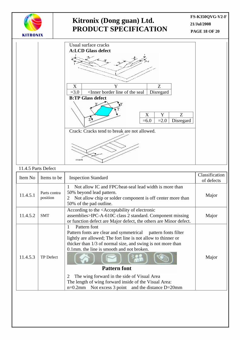
11.4.5 Parts Defect
Item No Items to be Inspection Standard Classification of defects
11.4.5.1 Parts contra position
、1 Not allow IC and FPC/heat-seal lead width is more than 50% beyond lead pattern. 、2 Not allow chip or solder component is off center more than
50% of the pad outline.
Major
11.4.5.2 SMT According to the <Acceptability of electronic assemblies>IPC-A-610C class 2 standard. Component missing or function defect are Major defect, the others are Minor defect.
Major
11.4.5.3 TP Defect
、 :1 Pattern font ,Pattern fonts are clear and symmetrical pattern fonts filter
lightly are allowed; The fort line is not allow to thinner or thicker than 1/3 of normal size, and swing is not more than 0.1mm. the line is smooth and not broken.
、 :2 The wing forward in the side of Visual Area
The length of wing forward inside of the Visual Area: ; , 。n=0.2mm Not excess 3 point and the distance D=20mm
Major
Pattern font
FS-K350QVG-V2-F
21/Jul/2008
PAGE 19 OF 20
Kitronix (Dong guan) Ltd. PRODUCT SPECIFICATION
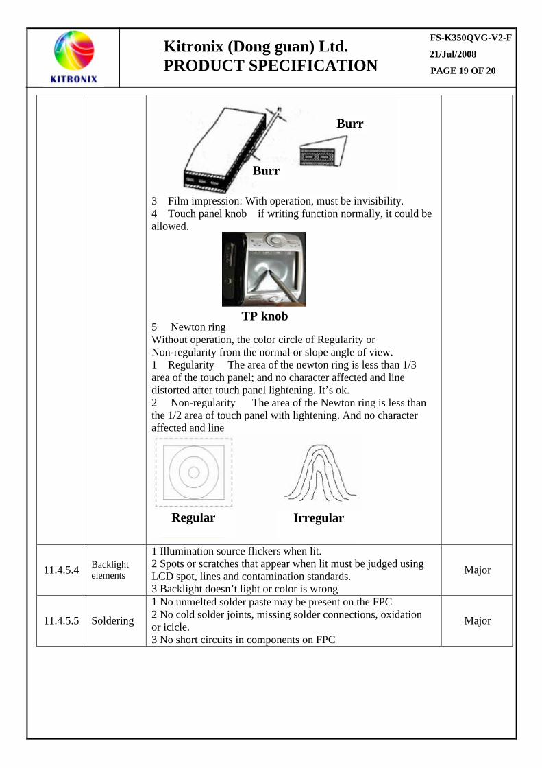
、3 Film impression: With operation, must be invisibility. 、 :4 Touch panel knob if writing function normally, it could be
allowed.
、5 Newton ring
Without operation, the color circle of Regularity or Non-regularity from the normal or slope angle of view. 、 :1 Regularity The area of the newton ring is less than 1/3
area of the touch panel; and no character affected and line distorted after touch panel lightening. It’s ok. 、2 Non- :regularity The area of the Newton ring is less than
the 1/2 area of touch panel with lightening. And no character affected and line
11.4.5.4 Backlight elements
1 Illumination source flickers when lit. 2 Spots or scratches that appear when lit must be judged using LCD spot, lines and contamination standards. 3 Backlight doesn’t light or color is wrong
Major
11.4.5.5 Soldering
1 No unmelted solder paste may be present on the FPC 2 No cold solder joints, missing solder connections, oxidation or icicle. 3 No short circuits in components on FPC
Major
Burr
Burr
TP knob
Regular Irregular

FS-K350QVG-V2-F
21/Jul/2008
PAGE 20 OF 20
Kitronix (Dong guan) Ltd. PRODUCT SPECIFICATION
11. Packing (Reference only)
Packing Method (1) 6pcs modules/tray (2) 6 tray stacking/lot
(3) 2 EPE cushion/lot (4) Fixing by type
(5) 1 lot/internal box (36PCS) (6) 6 internal boxs/out box
Size:383.0x270.0x66.0mm Size:570.0x410.0x265.0mm
Total: 216pcs module/out box
- END -
Covered by empty tray
6 tray/lot