Embed Size (px)
Citation preview
i
Kinetic Modeling of Intrinsic Stress in
Thin Films: The Effects of Processing
Parameters and Microstructure Evolution
by
Alison Engwall
Master of Engineering, Brown University, Providence, RI, 2012
Bachelor of Science, Massachusetts Institute of Technology, Cambridge, MA, 2009
A dissertation submitted in partial fulfillment of the requirements
for the degree of Doctor of Philosophy in the School of Engineering
at Brown University
Providence, Rhode Island
May 2018

ii
© Copyright 2018 Alison Engwall

iii
This dissertation by Alison Engwall is accepted in its present form by
the School of Engineering as satisfying the dissertation
requirement for the degree of Doctor of Philosophy.
Date ____________ __________________________________
Professor Eric Chason, Advisor
Recommended to the Graduate Council
Date ____________ __________________________________
Professor Brian Sheldon, Reader
Date ____________ __________________________________
Professor Pradeep Guduru, Reader
Approved by the Graduate Council
Date ____________ _______________________________
Andrew G. Campbell,
Dean of the Graduate School

iv
Curriculum Vitae
Alison Engwall received a B.S. in Materials Science and Engineering from the Massachusetts
Institute of Technology in 2009. After serving as a laboratory technician at the University of
Connecticut for two years, she enrolled in the Engineering graduate program at Brown University
graduate school and received an M.S. in Engineering in 2012. Prior to attending Brown, she
worked as an undergraduate researcher in MIT’s Chemical Oceanography Lab, at Pfizer, Inc as a
co-op intern, and at Pixtronix, Inc. While pursuing a Ph.D., she was a teaching assistant for both
graduate and undergraduate classes and a research assistant in Professor Eric Chason’s lab
studying intrinsic thin film stress.
Parts of this thesis have appeared in the following peer-reviewed publications:
1. E. Chason, A. Engwall, F. Pei, M. Lafouresse, U. Bertocci, G. Stafford, et al.,
"Understanding Residual Stress in Electrodeposited Cu Thin Films," Journal of The
Electrochemical Society, vol. 160, pp. D3285-D3289, January 1, 2013 2013.
2. E. Chason, J. Shin, C.-H. Chen, A. Engwall, C. Miller, S. Hearne, et al., "Growth of
patterned island arrays to identify origins of thin film stress," Journal of Applied Physics, vol. 115,
p. 123519, 2014.
3. E. Chason, A. Engwall, C. Miller, C.-H. Chen, A. Bhandari, S. Soni, et al., "Stress
evolution during growth of 1-D island arrays: Kinetics and length scaling," Scripta Materialia, vol.
97, pp. 33-36, 2015.

v
4. E. Chason and A. M. Engwall, "Relating residual stress to thin film growth processes via
a kinetic model and real-time experiments," Thin Solid Films, vol. 596, pp. 2-7, 2015.
5. A. Engwall, Z. Rao, and E. Chason, "Origins of residual stress in thin films: Interaction
between microstructure and growth kinetics," Materials & Design, vol. 110, pp. 616-623, 2016.
6. A. Engwall, Z. Rao, and E. Chason, "Residual Stress in Electrodeposited Cu Thin Films:
Understanding the Combined Effects of Growth Rate and Grain Size," Journal of The
Electrochemical Society, vol. 164, pp. D828-D834, 2017.
7. E. Chason, A. M. Engwall, Z. Rao, and T. Nishimura, "Kinetic model for thin film stress
including the effect of grain growth," Journal of Applied Physics, in press, 2018.

vi
Acknowledgements
There are many people who I am indebted to for their help and friendship over the course of my
studies, but first, my deep and sincere gratitude to my advisor Eric Chason for his years of
inspiration, encouragement, and support.
I would also like to express my sincere appreciation to my committee, Professors Brian Sheldon
and Pradeep Guduru, for their thoughtful comments and helpful discussions. I had the privilege of
working with and learning from many wonderful professors, and I must also single out Professor
Shreyes Mandre, who made Brown a brighter place.
To everybody that I shared a class, office, or lab with: thanks for the company and conversation. I
am glad to have known you. I was so lucky to get to work with everyone in Professor Chason’s
group, and my warmest thanks go out to Fei Pei, Chun-Hao Chen, and Zhaoxia Rao.
Finally, but most of all, my love and thanks to my parents, all the Moyers, and Nate, for everything.
This work was supported by the Office of Basic Energy Sciences, Division of Materials Sciences
and Engineering under Award No. #DE-SC0008799.

vii
Table of Contents
Signature Page ……………………………………………………………………………….. iii
Curriculum Vitae …………………………………………………………………………….. iv
Acknowledgements ...………………………………………………………………………… vi
Table of Contents ………………..…………………………………………………………... vii
List of Tables ..…………………………………………………………………………….…. x
List of Figures ...………………………………………………………………………….….. xi
Chapter 1: Introduction and Background …………………………………………………. 1
1.1 Overview of the thesis …………………………………………………………….. 2
1.2 Measuring stress with wafer curvature ……………………………………………. 4
1.3 Stress evolution during thin film deposition ……………………………………… 6
1.4 Proposed mechanisms for stress generation ………………………………………. 8
1.4.1 Tensile stress ……………………………………………………………. 8
1.4.2 Compressive stress ………………………………………………………. 10
References ……………………………………………………………………………... 11
Chapter 2: Kinetic Model …………………………………………………………………… 14
2.1 Visualization and formulation …………………………………………………….. 14
2.2 Application to experimental results ……………………………………………….. 20
References …………………………………………………………………………….. 21
Chapter 3: Experiments and Analysis …………………………………………………….... 22
3.1 Electrodeposition ………………………………………………………………….. 22
3.1.1 Substrate preparation ……………………………………………………. 22
3.1.2 Deposition ………………………………………………………………. 23
3.2 Wafer curvature measurement ……………………………………………………. 26
3.3 Grain size measurement …………………………………………………………… 28

viii
3.4 Fitting routines …………………………………………………………………….. 29
References ……………………………………………………………………………... 31
Chapter 4: Patterned Films …………………………………………………………………. 32
4.1 2D Symmetry ……………………………………………………………………… 32
4.1.1 Experiment ……………………………………………………………… 32
4.1.2 Model fitting …………………………………………………………….. 36
4.2 1D Symmetry ……………………………………………………………………… 41
4.2.1 Experiment ……………………………………………………………… 41
4.2.2 Curvature measurement …………………………………………………. 43
4.2.3 Fitting to kinetic model …………………………………………………. 46
4.3 Discussion ………………………………………………………………………… 53
4.4 Volmer-Weber film fit with 2D …………………………………………………… 55
References …………………………………………………………………………….. 60
Chapter 5: The Effect of Microstructure on Stress in Thin Films ………………………... 61
5.1 Zone model of microstructure evolution ………………………………………….. 61
5.2 Electrodeposited Ni: Zone 1 ………………………………………………………. 63
5.3 Electrodeposited Cu: Zone T ……………………………………………………… 69
References …………………………………………………………………………….. 76
Chapter 6: Stress evolution models for zone II microstructure …………………………... 77
6.1 Grain growth in zone II films ……………………………………………………... 78
6.2 Low mobility model ……………………………………………..………………... 79
6.2.1 Model fitting …………………………………………………………….. 81
6.3 High mobility model ………………………………………………….…………… 86
6.3.1 Model fitting …………………………………………………..………… 90
6.4 Discussion ………………………………………………………………….……... 94
References ………………………………………………………………………...…... 98
ix
Chapter 7: Conclusions …………………………………………………...…………………. 99
7.1 Summary of findings ………………………………………………………...……. 99
7.2 Analysis of parameters ……………………………………………………………. 101
7.2.1 Kinetic model plots of stress vs. two parameters ……………………….. 104
7.3 Future work ……………………………………………………………………….. 107
References ………………………………………………………………………...…... 109
Appendix A: Non-Linear Least Squares Fitting Programs ……………………………….. 110
A.1 Program for 2D symmetrical patterned film stress ………………………………. 111
A.2 Program for 1D symmetrical patterned film stress ………………………………. 123
A.3 Program for parametric stress surface ……………………………………………. 135
A.4 Program for zone II low mobility film stress …………………………………….. 141
A.5 Program for zone II high mobility film stress .…………………………………… 156
References …………………………………………………………………………….. 172

x
List of Tables
Table 4.1. 2D patterned film kinetic model fitting parameters for electrodeposited
Ni.
41
Table 4.2. Steady state 1D patterned kinetic model fit parameters for
electrodeposited Ni.
51
Table 4.3. 1D electrodeposited Ni patterned film kinetic model fitting parameters.
54
Table 4.4. 2D patterned film kinetic model fitting parameters for evaporated Ag.
57
Table 5.1. Kinetic model fitting parameters for steady-state paused
electrodeposited Ni.
69
Table 5.2. Kinetic model fitting parameters for continuously electrodeposited Ni. 69
Table 5.3. Kinetic model fitting parameters for steady-state electrodeposited Cu. 73
Table 6.1. Low mobility kinetic model fitting parameters for zone II evaporated
Ni.
84
Table 6.2. High mobility kinetic model fitting parameters for zone II evaporated
Ni.
93
Table 7.1. A summary of steady state kinetic model fitted parameters. All data is
for electroplated films.
101
Table 7.2. A summary of kinetic model fitted parameters for films deposited
continuously with the model fit to the full deposition stress thickness
curve. Rows marked with * are for e-beam evaporated films; all others
are electroplated.
102

xi
List of Figures
Figure 1.1. Wafer curvature measurements of Ag films evaporated on SiO2 wafer
substrates at 0.2 nm/s and temperatures as indicated on figure.
7
Figure 2.1. Schematic of structure and processes involved in film growth and stress
generation. Circles represent atoms on the surface, attaching to ledges,
and jumping into the triple junction where the grain boundary meets the
surface of the film, in the ith layer
15
Figure 3.1 Schematic of electrodeposition cell and MOSS setup. For wafer
curvature measurements, collimated laser beams reflected from the back
side of the substrate were picked up by CCD camera.
24
Figure 3.2. Deposition efficiency as a fraction of predictions from Faraday’s 2nd
law for Cu sulfate solution of 0.36 mol/L CuSO4 and 0.20 mol/L H2SO4
at 273 K.
26
Figure 3.3. Stress thickness vs thickness of Cu film electrodeposited at 0.96 nm/s
with periods of paused growth. Vertical dotted lines indicate pauses.
Inset: Stress thickness vs time for a segment of the deposition with the
periods of paused growth highlighted in grey.
27
Figure 3.4. a) Electrodeposited Cu with unannealed seed layer, showing grains of
increasing size, with an example line of intercepts such as those used to
calculate average grain size. b) Cu with annealed seed layer and stable
grain size.
28
Figure 4.1. Schematic cross-section of the multilayer structure used for 2D-
symmetric electrodeposition of Ni.
33
Figure 4.2. (a)-(c) Plane view SEM micrographs of patterned Ni films grown for
5400s to a radius of 9.9 μm, 6270s to a radius of 11.9 μm, and 7550s to
a radius of 14.5 μm, respectively. (d)-(f) Cross-sections of the islands
pictured in (a)-(c), correlating with the images above.
34
Figure 4.3. Schematic demonstrating three stages in the evolution of the geometry
of hemispherical islands growing in a LxL square grid. The radius of
the island is 𝜌 and the radius of the face is 𝑟. a) Prior to coalescence,
the island is hemispherical in shape, and 𝜌 < 𝐿/2. b) When 𝐿
2< 𝜌 <
√𝐿, flat semicircular faces form at the contact area between islands. c)
At 𝜌 > √𝐿, the island is a hemisphere truncated to a square base, and
the contact areas are rectangles with curved top edges.
34

xii
Figure 4.4. Thickness data for each deposition (solid lines) paired with calculated
island volumes (dashed lines). Deposition voltages of -1.39, -1.35, -
1.32, -1.31, and -1.29 V were found to produce constant radial growth
rates of 2.0, 2.9, 3.3, 4.1, and 5.1 nm/s respectively.
35
Figure 4.5. Stress thickness data measured by wafer curvature for the deposition of
Ni at several growth rates, as indicated on the figure. Solid blue lines
are the result of stress model fit discussed in the text.
37
Figure 4.6. Growth rates found by volumetric fitting vs. growth rates found by
linear approximation from the steady state.
38
Figure 4.7. Grain boundary velocity over time for hemispherical islands in a square
array with radial growth rates as indicated in the figure.
39
Figure 4.8. Cross section and sketch of a patterned electroplated Ni on Au.
42
Figure 4.9. Detailed schematic of semicylindrical island, post-coalesence.
44
Figure 4.10. Stress thickness vs thickness data (dots) and model fitting as described
in text (solid lines) for Ni films electrodeposited on patterned substrates
of parallel trenches (1D patterning) in arrays with a) 5.3 b) 10.6 and c)
26.5 μm spacing.
47
Figure 4.11. a) Illustration of the evolving relationship between the grain boundary
velocity, average height, and radius of coalescing islands of
semicircular cross-section as deposition progresses. b) Generalized plot
of grain boundary velocity with film thickness.
48
Figure 4.12. a) 𝜎𝑦𝑦,𝑆𝑆 for 1D patterned electrodeposited films with a fit to the model
estimating effective grain size as 500 nm. b) Steady state stress for
unpatterned electrodeposited films, with the same fit to model,
assuming a grain size of 150 nm.
50
Figure 4.13. Steady state total stress measured for 1D patterned films. Solid lines are
fit to model assuming 𝜎𝑇 ∝ 1/√𝐿 with 𝐿 as the pattern spacing.
52
Figure 4.14. Fitted steady state tensile parameters for patterned 1D films, fitted to a
line with 1/√𝐿 dependence.
52
Figure 4.15. Stress thickness of evaporated Ag deposited at 0.2 nm/s and a range of
temperatures as indicated on figure. Dark lines are a fit to the
hemispherical (2D) kinetic model with parameters presented in table
4.4.
56

xiii
Figure 4.16. Arrhenius plot of evaporated Ag parameter 𝛽𝐷 for lowest five
temperatures, 193-303 K.
58
Figure 4.17. Evaporated Ag deposited at 0.2 nm/s and a range of temperatures. Dark
lines for 323 and 373 K are drawn with parameters extrapolated from
those of lower temperature fits, while the thin lines are experimental
data.
59
Figure 5.1. Schematic of grain structure changing with thickness for different
regimes of atomic mobility, adapted from Thornton [1].
63
Figure 5.2. Deposition efficiency as a fraction of predictions from Faraday’s 2nd
law for Ni sulfamate solution of 0.36 mol/L Ni sulfamate and 0.65
mol/L boric acid at 273 K.
65
Figure 5.3. Electrodeposited Ni grain size vs thickness for two growth rates. Inset:
FIB micrograph showing columnar structure of film after 1 µm buffer
layer (demarcated by dotted line).
66
Figure 5.4. Electrodeposited Ni grain size vs thickness, growth rate vs thickness,
and stress thickness vs thickness for one experiment comprised of
subsequent layers deposited at several different growth rates in random
order, each repeated once after an initial 1 µm buffer layer.
67
Figure 5.5. Steady state stress of electrodeposited Ni fit to kinetic model described
in text.
68
Figure 5.6. Stress thickness of continuously electrodeposited Ni at a) 1.73 nm/s and
b) 0.42 nm/s with fit to kinetic model described in text (blue lines).
70
Figure 5.7. a) Grain size with thickness of two films grown at 0.44 nm/s to a total
thickness of 3 µm and 6 µm. b) FIB cross-section of 6 µm film. c) FIB
cross-section of 3 µm film.
71
Figure 5.8. a) Electrodeposited Cu stress-thickness vs. thickness for periods of
growth with rates indicated in figure and stress-thickness vs. time for
growth interrupts of approximately 120 s. Green lines are linear fits for
constant slope expected during steady-state growth; red lines are guides
to illustrate stress relaxation during growth pauses. b) FIB cross-section
micrograph of Cu film deposited including segments from (a). The
yellow band is an indication of where the growth interval in (a)
correlates to film thickness in the micrograph.
Figure 5.9. Electrodeposited Cu steady-state stress vs growth rate and grain size.
Stress was calculated from stress-thickness vs thickness measurements.
74

xiv
The function surface shows the kinetic model described in the text with
parameter values determined from fitting the data.
Figure 5.10. a-f) Electrodeposited Cu steady-state stress vs grain size at a growth
rate indicated on figure. Solid lines are a fit to model with parameters in
table 5.3.
75
Figure 5.11. a-d) Electrodeposited Cu steady-state stress vs growth rate at ranges of
grain size indicated on figure. Points are data averaged for each growth
rate with measured grain size within the given range. Solid and dashed
lines are a fit to model with parameters in table 5.3.
76
Figure 6.1. Stress thickness of evaporated Ni deposited at 373 K and a range of
growth rates as indicated on plot. Black lines are fit to low mobility
model for zone II microstructure described in text.
82
Figure 6.2. Stress thickness of evaporated Ni deposited at 0.05 nm/s and a range of
temperatures as indicated on plot. Black lines are fit to low mobility
model for zone II microstructure described in text.
83
Figure 6.3. (a) Low mobility kinetic model fitted parameter 𝜎𝐶 vs growth rate R for
evaporated Ni deposited at 373 K. (b) Arrhenius plot of ln(−𝜎𝐶) vs
1/kT for Ni deposited at 0.05 nm/s. Solid lines are linear fits.
85
Figure 6.4. Stress thickness of evaporated Ni deposited at 373 K and a range of
growth rates as indicated on plot. Black lines are fit to high mobility
model for zone II microstructure described in text.
91
Figure 6.5. Stress thickness of evaporated Ni deposited at 0.05 nm/s and a range of
temperatures as indicated on plot. Black lines are fit to high mobility
model for zone II microstructure described in text.
92
Figure 6.6. (a) High mobility kinetic model fitted parameter 𝜎𝐶 vs growth rate R
for evaporated Ni deposited at 373 K. (b) Arrhenius plot of ln(−𝜎𝐶) vs
1/kT for Ni deposited at 0.05 nm/s. Solid lines are linear fits.
94
Figure 6.7. Stress thickness of evaporated Ni deposited at 0.25 nm/s and 373K.
Dotted purple line and dashed blue line are fit to components of high
mobility model for zone II microstructure described in text; solid black
line represents the combined model.
96
Figure 7.1. Log-log plot of 𝛽𝐷 vs grain size for all fitted Ni experiments.
103
Figure 7.2. Evaporated Ni high mobility model surface for stress thickness vs
growth rate and temperature for a) film thickness h=15 nm, grain size
L=15 nm b) h=200, L=70. White plane is at 0 stress.
1.5
xv
Figure 7.3. Evaporated Ni high mobility model surface for stress thickness vs
thickness and temperature at a) 0.05 nm/s to a film thickness of 200 nm,
b) 0.05 nm/s to a film thickness of 600 nm, c) 0.03 nm/s to 200 nm and
b) 0.07 nm/s to 200 nm. White planes are at 0 stress.
106
Figure 7.4. Sputtered Mo plotted vs pressure and growth rate. The white plane is at
0 stress.
108

1
Chapter 1
Introduction and Background
Thin films of polycrystalline material are a key component in the manufacture of products from
microcircuitry with fine deposited copper connections to huge machined components with
protective solid coatings. An issue that affects every thin film application is the accumulation of
stress, which can begin during the deposition of material on the substrate. Stress generated during
deposition is called growth stress, residual stress, or intrinsic stress, in opposition to extrinsic
stresses such as from thermal expansion, applied forces, or epitaxial mismatch, which are not
explored in this thesis. If too much stress builds up in a film, stress can change the desired
properties of the film, cause warping in the substrate underneath, or lead to defects like cracking
or delamination, any of which can cause device failure. Therefore, it is imperative to control stress
generation in many applications. Toward this end, the development of a model to describe and
predict how and why stress is generated during film growth provides a powerful tool in device
manufacturing and an aid to deepen physical understanding of the basic processes. This is the
underlying purpose of the work presented here: investigation into how stress develops in several
deposition systems with the goal of describing stress development using a robust model based on
fundamental principles. Experiments investigating the effects of deposition rate, geometry,
temperature, and microstructure evolution on stress development were analyzed using the
framework of a kinetic model based on atomic interactions in the growing film, especially where
the surface of the film forms triple junctions with the boundaries between grains.
2
1.1 Overview of the thesis
The current chapter will serve as an introduction to the important principles of the study of intrinsic
stress. Relating substrate curvature to stress in a thin film is covered first, with a discussion of the
body of published experiments and observations. Then follows a brief history of developments in
the theory of stress generation mechanisms for both tensile and compressive stress, which guided
the development of the kinetic model we use to understand how film stress relates to experimental
conditions and kinetic parameters.
An explanation of the fundamental kinetic model is detailed in chapter 2. This model forms the
basic framework which is used to self-consistently describe the stress behavior of experiments in
later chapters with respect to film geometry, deposition parameters, and internal microstructure.
The essential basis of the model lies in two competing mechanisms for tensile and compressive
stress generation which occur simultaneously at the triple junction where a grain boundary meets
the surface of a film. The foundations of the model laid out in chapter 2 are expanded or adapted
in later chapters to encompass additional sources of stress such as grain growth or more complex
growth conditions such as high atomic mobility.
Experimental techniques for Cu electrodeposition with simultaneous wafer curvature
measurement are presented in chapter 3, along with the procedures used for analyzing the
deposited films. Stress measurements were performed in situ with a multi-beam optical stress
sensor (MOSS) array. Grain size measurements were performed with Focused Ion Beam (FIB)
cross-sections of deposited films. A discussion of the principles and methodology behind the non-

3
linear least squares fitting routines written in Matlab for fitting experimental data to the kinetic
model outlined in chapter 2 is included as well.
Chapter 4 considers several sets of stress measurements taken from Ni films electrodeposited onto
photolithographically patterned substrates, which resulted in geometrically controlled films with
uniform 1. Biaxially symmetric hemispherical islands or 2. Axially symmetric hemicylindrical
islands that coalesced in one simultaneous event across the film. The kinetic model is applied as a
tool for understanding the stress from coalescence of the islands, stresses observed pre-
coalescence, and the steady state stresses once films became uniform.
Uniform electrodeposited films in the steady state regime well past the point of coalescence were
deposited at a range of growth rates and analyzed with detailed grain size measurements in order
to explore the interdependent relationship between grain size, growth rate, and stress. These
experiments and results are presented in chapter 5. The influence of surface grain size on stress
development is separated from the stress caused directly by grain growth. Two types of
microstructure are detailed: Ni films show minimal increase in grain size with film thickness, while
the grain size of Cu films increases at the surface as films are deposited.
In chapter 6, the kinetic model introduced in chapter 2 is adapted to higher mobility systems where
substantial grain growth occurs in the bulk of the film. A series of Ni films deposited by electron
beam evaporation over a range of growth rates and a range of temperatures are well-described and
analyzed with two formulations of the model. The results suggest that, in some regimes,
compressive stress generation mechanisms may depend on deposition rate and temperature much
more strongly than previously suspected, and that the atomic exchange between the surface and
4
the grain boundary may not be directly analogous to either diffusion across a surface or diffusion
internally along a grain boundary.
Finally, a summary and discussion of findings as well as proposals for future work are presented
in chapter 7. An overview and analysis of trends observed in kinetic parameters across analyzed
experiments suggests further unexpected dependencies on grain size. Additional studies describing
the stress evolution of other materials, extension of the kinetic model to energetic deposition
systems, and detailed atomistic computational modeling of the junction between grain boundaries
and the film surface are all promising avenues for further investigation.
1.2 Measuring stress with wafer curvature
Stress arises when a thin film well-adhered to a rigid substrate experiences a change in state which
leads to a change in film density [1, 2]. Thus processes such as thermal expansion, defect
annihilation, or phase change which would change the volume of a free-standing film can generate
stress in a film attached to a substrate unaffected by the same processes [3]. However, sufficient
buildup of stress in a film can lead to warping of the substrate underneath. While substrate
deformation can be a problem in commercial applications, measurements of substrate curvature
are a common method for indirectly determining the average stress in a film. This practice was
first quantified by Stoney [4], who measured the bending of a “thin steel rule” electrodeposited
with Ni and related the resulting curvature to the thickness of the film with the elastic modulus of
Ni. The only substantial change to the formula in the last hundred years is that instead of the bulk

5
elastic modulus E, we use the biaxial modulus 𝑀𝑠 =𝐸
(1−𝜈) where 𝜈 is Poisson’s ratio, with the
assumption that the in-plane stress is biaxially symmetric. We relate the curvature of the substrate,
𝜅, to the average stress in the film, ⟨𝜎⟩ with the equation [5]
𝜅 =6⟨𝜎⟩ℎ𝑓
𝑀𝑠ℎ𝑠2
, (1.1)
where ℎ𝑓 is the height of the thin film and ℎ𝑠 is the thickness of the substrate. The average stress
in the film can be found by integrating the stress through the film thickness:
⟨𝜎⟩ =1
ℎ𝑓∫ 𝜎(𝑧)𝑑𝑧, (1.2)
ℎ𝑓
0
where 𝑧 is the direction normal to the substrate and 𝜎(𝑧) is the stress at a particular height in the
film. The quantity ⟨𝜎⟩ℎ𝑓 is known as the stress thickness or force per unit width (𝐹/𝑤), which is
proportional to the curvature as per equation 1.1. The exact value of 1/𝑀𝑠 reported for (001) Si is
180.3 GPa [6].
It is important to note that the curvature of the wafer is determined by the average stress in the
film. If the stress is not distributed uniformly, it is impossible to determine from a single
measurement what the stress is at any given height in the film. However, if continuous
measurement is made of how the substrate curvature changes over time, the slope or derivative of
the data will show how the stress is changing at any particular point. In cases where the stress after
deposition does not change in the bulk of the film (𝜕𝜎(𝑧, 𝑡) = 0), that incremental or instantaneous
stress relates to the stress in the new sliver of film deposited at that given time. That is, as derived
in [7]:

6
𝜎(ℎ𝑓) ∝𝑑𝜅
𝑑𝑡. (1.2)
Or, combined with equation 1.1,
𝜎(ℎ𝑓) =𝑑
𝑑𝑡
6⟨𝜎⟩ℎ𝑓
𝑀𝑠ℎ𝑠2
. (1.3)
If the growth rate of the average height of the film is known, 𝑑ℎ𝑓/𝑑𝑡, then the equation
𝜎(ℎ𝑓) ∝
𝑑⟨𝜎⟩ℎ𝑓
𝑑𝑡𝑑ℎ𝑓𝑑𝑡
=𝑑⟨𝜎⟩ℎ𝑓
𝑑ℎ𝑓 (1.4)
relates the stress in the most recently deposited layer to the instantaneous stress in the film, which
can be found by measuring the slope on a plot of stress thickness vs. thickness. An example plot
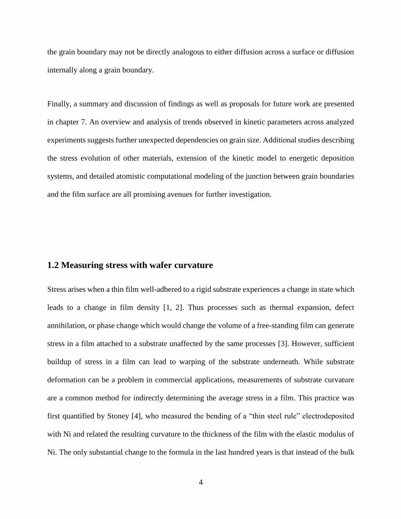
of stress thickness vs. thickness for a typical set of wafer curvature experiments is shown in Fig
1.1 for Ag films deposited on SiO2 at a range of temperatures, from data previously presented in
[8].
1.3 Stress evolution during thin film deposition
In a Volmer-Weber thin film, atoms deposited on a substrate nucleate islands of small clusters of
atoms which increase in size with additional material until the islands coalesce to create a uniform
film [9-12]. These films are characterized by three distinct regimes of morphology which correlate
with commonly observed trends in stress evolution [13]. As material is deposited on a substrate,
initial independent island nucleation is correlated with very low observed stress. When islands
grow to sufficient size to impinge on each other and begin to coalesce, this stage is associated with
7
a sharp tensile rise in stress thickness [14]. Thickness is measured as average thickness, though
the actual morphology of films in these early stages is uneven, with islands several atomic layers
thick separated by bare substrate. Finally, a whole, uniform film is formed. Once a film reaches a
steady state past the point of coalescence where the shape of the surface is unchanging with film
thickness, the stress thickness may either remain tensile, with a positive slope, or become
compressive, with a negative slope. Films with an initially compressive slope may also become
less compressive as thickness increases. In the plot shown in figure 1.1, films deposited at all
temperatures experience a tensile stress associated with film coalescence before 40 nm thickness,
Figure 1.1. Wafer curvature measurements of Ag films evaporated on SiO2 wafer substrates
at 0.2 nm/s and temperatures as indicated on figure.
8
but increasing temperatures correlate with more compressive stress in the films afterward. Koch
and Abermann et al [15-18] theorized that film growth characterized by only tensile stress, Type
I behavior, and films which underwent tensile-compressive stress evolution, Type II behavior,
were differentiated by atomic mobility. They observed that low-mobility Volmer-Weber growth
was commonly associated with Type I tensile films and high-mobility Volmer-Weber growth lead
to tensile-compressive Type II behavior.
However, mobility is not the only variable which affects whether films develop tensile or
compressive stress. Hearne and Floro performed experiments with electrodeposited Ni films which
found that varying the deposition rate between 1.4 and 14 nm/s in a sulfamate bath held at 313 K
produced films with Type I behavior at high deposition rates and Type II behavior at low
deposition rates [19]. Another parameter which affects film stress even when considered
independent of atomic mobility is grain size [20]. Several mechanisms have been proposed in
efforts to explain these and other observations of how stress depends on deposition parameters and
microstructure development.
1.4 Proposed mechanisms for stress generation
1.4.1 Tensile stress
A commonly accepted mechanism for the creation of tensile stress was first introduced by
Hoffman to explain stress generated during island coalescence [21]. This model relies on the
balance between the free surface energy of neighboring independent islands and the sum of the
9
interfacial energy between the two surfaces drawn into contact with each other and the strain
energy left in each island by the attraction and “snapping together” of the adjacent surfaces. Just
as this balance may be applied to adjacent islands, it may also be applied to adjacent but
independent atomic terraces in neighboring grains [22, 23]. As the two steps are drawn together to
create a new segment of grain boundary, strain is created in the step interiors. If the strain is
distributed uniformly over the area of the entire island or grain of width 𝐿, geometric constraints
predict tensile stress generation proportional to √Δ𝛾
𝐿, where Δ𝛾 is the difference in energy between
two free surfaces and one grain boundary. Other models have been proposed, but all rely on the
same basic energy balance [23, 24, 25]. Notably, Nix and Clemens applied the principles of
Griffith’s model of incremental crack propagation to grain boundary formation between islands,
and they also arrived at a 1
√𝐿 relation [26]. From a practical standpoint, this means that films with
smaller grains would be predicted to have a higher tensile stress, all other factors being equal,
because more grain boundaries are being formed during coalescence.
Another important source of tensile stress in thin films is grain boundary annihilation during grain
growth, which transforms a volume of lower density disordered grain boundary to one of higher
density incorporated into the lattice, as first proposed by Chaudhari [27]. Briefly, if the strain
caused by the grain growth is isotropic, the consequential in-plane stress is
𝜎𝑔𝑔 = 𝑀𝑓Δ𝑎 (1
𝐿0−
1
𝐿). (1.5)
𝐿0 is the initial grain size, and Δ𝑎 is defined as the excess volume per unit area of grain boundary,
also called the grain boundary width. This densification thanks to grain boundary annihilation,
along with additional tensile stress from vacancies and other low-density defects being swept up
10
and absorbed by grain boundaries in motion, can occur during deposition, afterward, or both. The
rate and ease of densification depends on the atomic mobility of the film, and therefore on the
temperature. However, since grain growth generates only tensile stress, it is impossible to explain
the full range of observed stress evolution behaviors with only grain growth effects. Grain growth
and microstructure evolution are important to consider and account for in high-mobility systems
and will be discussed more in later chapters.
1.4.2 Compressive stress
Over the last few decades, several mechanisms for compressive stress development have been put
forward and debated by various groups, in search of a satisfactory explanation. Abermann and
Koch suggested that low melting point metal films develop compressive strain at the interface with
the substrate due to surface tension effects distorting the lattices before the films fully coalesce,
and that the resulting stress perpetuates as the thickness of the films increases [15,28,29].
However, Friesen and Thompson demonstrated that pre-coalescence compressive stress is up to
90% reversible during a pause in deposition, which would not affect a strain maintained at the
interface [30]. They proposed instead that compressive stress arises from excess adatoms on the
surface being incorporated into the film when deposition stops, causing a decrease in the
compressive stress [30,31]. An important observation in support of this theory is that a pre-
coalescence and post-coalescence pause during evaporation of a Cu film generated similar
reductions in the compressive stress. In an experiment published by Spaepen [32], a similar
deposition of Cu with three growth interrupts has post-coalescence interrupts with tensile stress
increase or compressive stress reduction of three times and six times the size of the pre-coalescence
increase. Since there should not be a dramatic change in the saturation of adatoms on the surface,
this suggests other mechanisms are at work, especially because adatom effects alone cannot

11
explain a steady-state compressive stress in a continuous film. Spaepen in turn proposed that
excess compressive ledges may consolidate during interrupts, leading to a reversible reduction in
compressive stress, and that excess atoms being incorporated into the topmost layer of the film
between two such ledges may lead to a compressive steady-state stress.
Existing grain boundaries are a more common and effective sink for adatoms than new defect
generation, though other defects may play a role in assisting or inhibiting adatom diffusion. Nix
and Clemens advanced the idea that tensile strain generated during the adjacent-grain zipping
process could be ameliorated by adatom insertion into the grain boundaries [26]. Chason, Sheldon,
Freund, Floro, and Hearne used the same idea to create an integrated model for both tensile and
compressive stress generation based on fundamental, universal processes that take place at the
triple junction where a grain boundary meets the surface of a growing film [33]. This model,
described in the next chapter, forms the basis of our analysis of the interrelated effects of growth
rate, geometry, and microstructure on stress evolution.
References
[1] M. F. Doerner and W. D. Nix, Critical Reviews in Solid State and Materials Sciences 14
(3), 225-268 (1988).
[2] W. D. Nix, Metallurgical and Materials Transactions A 20 (11), 2217-2245 (1989).
[3] R. Hoffman, Academic, New York, 211 (1966).
[4] G. G. Stoney, Proceedings of the Royal Society of London. Series A, Containing Papers of
a Mathematical and Physical Character 82 (553), 172-175 (1909).
[5] L. B. Freund and S. Suresh, Thin film materials: stress, defect formation and surface
evolution. (Cambridge University Press, 2004).

12
[6] G. Janssen, M. Abdalla, F. Van Keulen, B. Pujada and B. Van Venrooy, Thin Solid Films
517 (6), 1858-1867 (2009).
[7] E. Chason, Thin Solid Films 526, 1-14 (2012).
[8] E. Chason, J. Shin, S. Hearne and L. Freund, Journal of Applied Physics 111 (8), 083520
(2012).
[9] C. V. Thompson, Annual Review of Materials Science 30 (1), 159-190 (2000).
[10] M. Ohring, Materials science of thin films. (Academic press, 2001).
[11] P. H. Mayrhofer, C. Mitterer, L. Hultman and H. Clemens, Progress in Materials Science
51 (8), 1032-1114 (2006).
[12] I. Petrov, P. B. Barna, L. Hultman and J. E. Greene, Journal of Vacuum Science &
Technology A: Vacuum, Surfaces, and Films 21 (5), S117-S128 (2003).
[13] J. A. Floro, E. Chason, R. C. Cammarata and D. J. Srolovitz, MRS bulletin 27 (01), 19-25
(2002).
[14] R. Cammarata, T. Trimble and D. Srolovitz, Journal of Materials Research 15 (11), 2468-
2474 (2000).
[15] R. Abermann and R. Koch, Thin Solid Films 129 (1-2), 71-78 (1985).
[16] R. Koch, Journal of Physics: Condensed Matter 6 (45), 9519 (1994).
[17] R. Abermann, R. Koch and H. Martinz, Vacuum 33 (10-12), 871-873 (1983).
[18] G. Thurner and R. Abermann, Thin Solid Films 192 (2), 277-285 (1990).
[19] S. J. Hearne and J. A. Floro, Journal of applied physics 97 (1), 014901 (2005).
[20] R. Koch, D. Hu and A. Das, Physical review letters 94 (14), 146101 (2005).
[21] R. Hoffman, Thin Solid Films 34 (2), 185-190 (1976).
[22] S. C. Seel, C. V. Thompson, S. J. Hearne and J. A. Floro, Journal of Applied Physics 88
(12), 7079-7088 (2000).
[23] L. B. Freund, E. Chason and R. W. Hoffman, Journal of Applied Physics 89 (9), 4866-
4873 (2001).
[24] A. Rajamani, B. W. Sheldon, E. Chason and A. F. Bower, Applied physics letters 81 (7),
1204-1206 (2002).
[25] J. S. Tello, A. F. Bower, E. Chason and B. W. Sheldon, Physical review letters 98 (21),
216104 (2007).
[26] W. Nix and B. Clemens, Journal of Materials Research 14 (08), 3467-3473 (1999).

13
[27] P. Chaudhari, Journal of Vacuum Science and Technology 9 (1), 520-522 (1972).
[28] R. Abermann, Vacuum 41 (4-6), 1279-1282 (1990).
[29] R. Koch, D. Hu and A. K. Das, Physical Review Letters 94 (14), 146101 (2005).
[30] C. Friesen and C. Thompson, Physical review letters 89 (12), 126103 (2002).
[31] C. Friesen and C. Thompson, Physical review letters 93 (5), 056104 (2004).
[32] F. Spaepen, Acta Materialia 48 (1), 31-42 (2000).
[33] E. Chason, B. Sheldon, L. Freund, J. Floro and S. Hearne, Physical Review Letters 88 (15),
156103 (2002).
14
Chapter 2
Kinetic Model
A successful model for complex physical processes is one that captures the essential behavior of
the system using simplified, quantifiable elements. As such, the goal in developing a kinetic model
is primarily to capture the crucial trends and dependencies with a necessarily incomplete
simulacrum which nonetheless fundamentally correctly represents the dominant physical
processes. Thin films during deposition are dynamic systems, and many processes occur
simultaneously in competition and cooperation to produce stress in a film. Atomic diffusion across
terraces and step edges, interactions with the substrate, defect creation and annihilation, grain
boundary motion, thermal stresses, large or small impurities, deposition conditions, and surface or
solution or atmosphere chemistry all undoubtedly have some effect on how stress in a film
develops. The model described in this chapter focuses on basic processes of film growth and
atomic diffusion occurring at the critical location of the triple junction where two independent
planes of atoms meet, join, and form a new segment of grain boundary.
2.1 Visualization and formulation
To quantify the fundamental physical processes underpinning the kinetic model, it is useful to
consider film growth as a layer-by-layer process, represented in schematic in figure 2.1. Adatoms
deposited on the surface of a polycrystalline film diffuse across the surface, occasionally
nucleating new islands of atomic layers, or attaching to existing step ledges and advancing the

15
leading edge of the step. Following the Hoffman-Nix-Clemens model for tensile stress generation
from the formation of new grain boundary, when ledges on neighboring grains approach each
other, the two free surfaces cohere by snapping together, creating strain energy in the layer [1-4].
The change in interfacial energy Δ𝛾 from the elimination of a free surface for each grain in
exchange for one shared segment of grain boundary is
Δ𝛾 = 𝛾𝑠 −1
2𝛾𝑔𝑏, (2.1)
where 𝛾𝑠 and 𝛾𝑔𝑏 are the interfacial energies of the step edge and the grain boundary, respectively.
Assuming biaxial symmetry in the film, the change in energy of each grain of diameter 𝐿 as a layer
coalesces is, for the surface transformation alone, adapted from [5],
Δ𝑈𝑔𝑏 = −4𝐿𝑎Δ𝛾. (2.2)
Deposition flux
ith
layer
a
triple junction
grain boundary
ℎ𝑔𝑏 = 𝑎𝑖
Figure 2.1. Schematic of structure and processes involved in film growth and stress generation.
Circles represent atoms on the surface, attaching to ledges, and jumping into the triple junction
where the grain boundary meets the surface of the film, in the ith layer.

16
However, elimination of the separation between the two grains to form the grain boundary also
leaves a strain energy in the film,
Δ𝑈𝑠𝑡𝑟𝑎𝑖𝑛 = 𝑎𝐿2𝜎𝑇,𝑖
2
𝑀𝑓 (2.3)
using the approximation of square grains. 𝑎, as in the schematic, is the width of an atom or the
height of an atomic layer. 𝜎𝑇 is the tensile stress created in the film, and 𝑀𝑓 is the biaxial modulus,
𝐸
1−𝜈, where 𝐸 is Young’s modulus and 𝜈 is Poisson’s ratio for the material being deposited. In order
for grain boundary creation to be energetically favorable,
Δ𝑈𝑔𝑏 + Δ𝑈𝑠𝑡𝑟𝑎𝑖𝑛 < 0. (2.4)
Solving for 𝜎𝑇 gives
𝜎𝑇,𝑖 < 2 (𝑀𝑓
Δ𝛾
𝐿)
1/2
. (2.5)
The tensile stress in the layer produced by coalescence is thus proportional to 1
√𝐿.
When the new segment of grain boundary is formed, adatoms on the film surface can jump into
the newly created triple junction, alleviating tensile stress or generating compressive stress. The
change in strain for layer i with the addition of 𝑁𝑖 atoms can be written as
Δ휀𝑖 = −𝑁𝑖𝑎
𝐿, (2.6)
which is negative because the strain is compressive. Applying Hooke’s law, the compressive stress
in layer i from atom insertion is

17
σ𝐶,𝑖 = −𝑀𝑓
𝑁𝑖𝑎
𝐿. (2.7)
Note that in high-mobility systems, diffusion through the grain boundary allows inserted atoms to
distribute evenly among previously deposited layers, so that stress in the film remains uniform.
Atoms that jump from the surface into the triple junction are free to leave the topmost layer of the
grain boundary to diffuse deeper into the film, which means that it is impossible to analyze stress
development on a layer-by-layer basis considering only the triple junction and not the film as a
whole. A specific formulation for high-mobility systems will be discussed in chapter 6. Here,
formulation of the kinetic model applies to low-mobility systems where atoms do not diffuse
between layers and stress change is limited to the topmost layer of the film.
The number of atoms that have the opportunity to jump from the surface into the grain boundary
is limited by the time that the grain boundary is exposed to the surface before the next layer of
atoms snaps together on top of it, forming a new triple junction. The driving force for atoms to
make the jump is Δ𝜇, the difference in chemical potential between atoms in the grain boundary
and those on the surface. From [5], the equation which predicts the rate at which atoms join the
topmost layer by jumping from the surface to the triple junction can be written as
𝜕𝑁𝑖
𝜕𝑡= 4𝐶𝑠
𝐷
𝑎2(1 − 𝑒
−Δ𝜇𝑘𝑇 ) = 4𝐶𝑠
𝐷Δ𝜇
𝑎2𝑘𝑇, (2.8)
where 𝐷 is an effective diffusivity for the transition between the surface and the triple junction, 𝐶𝑆
represents the fractional concentration of adatoms on the surface, 𝑘 is the Boltzmann constant, and
𝑇 is the temperature. These parameters contribute to how many atoms can jump, and how quickly.
Expression 2.8 represents a simplification of the stress fields around the triple junction and the

18
value of parameters such as Cs and D are not well known, but this framework provides a basis of
kinetic parameters and relations to consider.
The driving force for atom insertion, Δ𝜇, has several contributing factors. First, deposition
processes are by their nature non-equilibrium states. In equilibrium, there is no net flux of atoms
onto or off of the surface or into or out of the grain boundaries. Deposition introduces more atoms
onto the surface than would exist at equilibrium. The chemical potential difference on the surface
due to this extra saturation of atoms contributes to the difference that drives atoms from the surface
into the grain boundaries. Additionally, existing stress in the film will affect the chemical potential
of the grain boundary. Tensile strain energy, such as from grain boundary formation, can be
alleviated by atom insertion. Conversely, compressive stress will increase the chemical potential
energy of atoms in the grain boundary, even to the point where atoms jump out. The chemical
potential energy from stress is equal to −σ𝑖Ω, where Ω = 𝑎3, the volume of an atom, and the term
is negative so that adding atoms to a layer increases compressive stress. The expression for the
chemical potential difference between the surface and the grain boundary is then
Δ𝜇 = 𝜇𝑠 − 𝜇𝑔𝑏 = 𝛿𝜇𝑠 + σ𝑖Ω, (2.9)
Other factors unaccounted for may contribute to Δ𝜇 as well, such as surface morphology,
impurities, other defects, or grain boundary mismatch angle.
The stress in each layer i can be found by combining equations 2.5 and 2.7:
σ𝑖 = σ𝑇 − 𝑀𝑓
𝑁𝑖𝑎
𝐿. (2.10)
Incorporating equation 2.8 results in an ordinary differential equation which describes the stress
generated in the ith layer of the film over time:
19
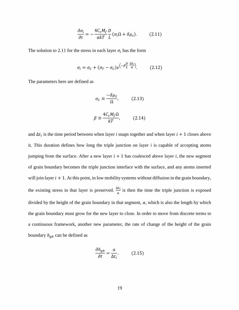
𝜕𝜎𝑖
𝜕𝑡= −
4𝐶𝑠𝑀𝑓
𝑎𝑘𝑇
𝐷
𝐿(𝜎𝑖Ω + 𝛿𝜇𝑠). (2.11)
The solution to 2.11 for the stress in each layer 𝜎𝑖 has the form
𝜎𝑖 = 𝜎𝐶 + (𝜎𝑇 − 𝜎𝐶)𝑒(−𝛽𝐷𝐿
Δ𝑡𝑖𝑎
). (2.12)
The parameters here are defined as
𝜎𝐶 ≡−𝛿𝜇𝑆
Ω, (2.13)
𝛽 ≡4𝐶𝑠𝑀𝑓Ω
𝑘𝑇, (2.14)
and Δ𝑡𝑖 is the time period between when layer i snaps together and when layer 𝑖 + 1 closes above
it. This duration defines how long the triple junction on layer i is capable of accepting atoms
jumping from the surface. After a new layer 𝑖 + 1 has coalesced above layer i, the new segment
of grain boundary becomes the triple junction interface with the surface, and any atoms inserted
will join layer 𝑖 + 1. At this point, in low mobility systems without diffusion in the grain boundary,
the existing stress in that layer is preserved. Δ𝑡𝑖
𝑎 is then the time the triple junction is exposed
divided by the height of the grain boundary in that segment, 𝑎, which is also the length by which
the grain boundary must grow for the new layer to close. In order to move from discrete terms to
a continuous framework, another new parameter, the rate of change of the height of the grain
boundary ℎ𝑔𝑏 can be defined as
𝜕ℎ𝑔𝑏
𝜕𝑡=
𝑎
Δ𝑡𝑖. (2.15)

20
This term is also referred to as the grain boundary velocity, and it is determined by the growth rate
and the geometry of the film. Experiments performed with controlled film geometry will be
discussed in chapter 4. For a fully coalesced, uniform film, the grain boundary velocity can be
approximated by the average growth rate for the film, 𝑅. The stress per layer for low mobility films
in the steady state well past the point of coalescence is then
𝜎𝑖 = 𝜎𝐶 + (𝜎𝑇 − 𝜎𝐶)𝑒(−
𝛽𝐷𝑅𝐿
). (2.16)
R and L are experimental parameters which can be controlled or measured, and 𝜎𝐶, 𝜎𝑇, and 𝛽𝐷
are kinetic parameters which can only be determined by applying the model to experimental results
and obtaining best fit values. Non-linear least squares fitting programs were developed in order to
use this model to describe stress evolution during film growth for several sets of experiments, as
described in the following chapters. The influence of growth rate, microstructure, island
coalescence, temperature, and grain boundary mobility are all explored with variations or
extensions of this fundamental model.
2.2 Application to experimental results
Since stress cannot be measured directly, we depend on curvature measurements for insight into
stress states in growing films. Measurements of wafer curvature during film deposition provide
two types of information about the stress and the evolution of stress in the film. First, the curvature
measured is directly proportional to the stress thickness of the film, as in equation 1.1. Second, the
derivative of the stress thickness gives the instantaneous stress in the film. For a low mobility
system where the stress is only changing in the topmost layer of the film, the instantaneous stress

21
is directly applicable to the expression for stress in a single atomic layer presented in equation
2.12, that is, 𝜎(ℎ𝑓) = 𝜎𝑖.
The total stress in a film can be found by integrating the stress in each layer over the film thickness:
⟨𝜎⟩ℎ𝑓 = ∫ 𝜎(ℎ)𝑑ℎℎ𝑓
0
. (2.17)
This stress thickness can be compared directly to the stress thickness calculated from wafer
curvature measurements. The next chapter will detail both the methodology of the deposition
experiments and the fitting procedures used to find parameter values and evaluate how well the
model can describe the complex stress evolutions and dependencies observed during deposition.
References
[1] R. Hoffman, Thin Solid Films 34 (2), 185-190 (1976).
[2] S. C. Seel, C. V. Thompson, S. J. Hearne and J. A. Floro, Journal of Applied Physics 88
(12), 7079-7088 (2000).
[3] L. B. Freund, E. Chason and R. W. Hoffman, Journal of Applied Physics 89 (9), 4866-
4873 (2001).
[4] W. Nix and B. Clemens, Journal of Materials Research 14 (08), 3467-3473 (1999).
[5] E. Chason, Thin Solid Films 526, 1-14 (2012).

22
Chapter 3
Experiments and Analysis
This chapter describes the experimental procedures followed for Cu electrodeposition performed
with simultaneous wafer curvature measurement and the methodology of analysis for the films and
data after deposition. Wafer curvature was monitored with a multi-beam optical stress sensor
(MOSS), which is detailed, and grain size analysis was accomplished for deposited films with
focused ion beam (FIB) cross-sections and imaging. The final section discusses the non-linear least
squares fitting programs designed to fit experimental data to the kinetic model introduced in
chapter 2.
3.1 Electrodeposition
3.1.1 Substrate preparation
The Cu films for stress measurement experiments had a multilayer structure consisting of a Si
wafer substrate with a Ti adhesion layer and a Cu seed layer deposited by physical vapor deposition
(PVD). The Si wafers, oriented along the (100) axis and polished on both sides, had a natural SiO2
oxide coating. They were cut into rectangular sections approximately 40 mm in length and 10 mm
in width with a thickness ranging from 150 to 300 μm.
Prior to PVD coating, the substrates were cleaned following an industry standard procedure. In a
clean room environment, they were subjected to ultrasonic agitation in successive baths of acetone,

23
methanol, and isopropanol, for five minutes each, repeated as necessary. Finally, they were dried
with compressed nitrogen gas, mounted on a sample holder, and transferred to the PVD chamber,
a Kurt J. Lesker LAB 18 Modular Thin Film Deposition System.
Ti and Cu were deposited by electron beam (e-beam) evaporation. Pellets produced by the Kurt J.
Lesker company with a purity of 99.995% provided material for evaporation. Growth rates and
total deposited film thickness were monitored with the aid of a quartz crystal microbalance sensor.
Ti was deposited first, at the rate of 1 Å/s, to a thickness of 15-20 nm. Cu was deposited at a rate
of 1-2 Å/s, with a final thickness typically between 120 and 200 nm, but up to 600 nm. Samples
with 600 nm evaporated Cu layers were annealed on a hot plate at 150 °C for 1-5 minutes to
encourage grain growth prior to electrodeposition and stress measurement. Because of the
tendency of electrodeposited Cu to inherit the grain size and orientation of the previously deposited
layer, this annealing process affected the initial grain size of the deposited films. Immediately
before electrodeposition, samples were gently agitated in 98% sulfuric acid to remove any copper
oxide that may have developed on the evaporated coating, then rinsed in deionized water and dried
with compressed nitrogen gas.
3.1.2 Deposition
Electrodeposition from a Cu sulfate bath was conducted with simultaneous wafer curvature
measurement. A schematic for the experimental setup is shown in figure 3.1. The three-electrode
design of the plating cell is comprised of three electrodes, a PTFE sample holder, and an acid-
resistant acrylic tank. Details of the design can be found in [1]. As labelled on the schematic, the
electrodes are (1) a reference electrode, (2) a counter electrode, and (3) a working electrode in
contact with the previously deposited PVD layer on the Si substrate. The reference electrode used

24
was a saturated calomel (SCE) reference electrode, and the counter electrode was a Pt gauze
submerged in solution parallel to the deposition surface. The working electrode in contact with the
sample was a copper rod, polished at each end before electrodeposition to ensure good contact.
Cu was deposited from an electrolyte solution of 0.36 mol/L CuSO4 and 0.20 mol/L H2SO4, clear
and dark blue in color. Galvanostatic control was used to ensure that deposition rate, rather than
driving force, was constant. A model 263A potentiostat produced by Princeton Applied Research
was used for this procedure. Plating current ranged from 0.6 to 30 mA/cm2, resulting in deposition
rates of 0.22 to 11.02 nm/s in very good agreement with the predictions of Faraday’s Laws. After
1 2 3
Laser CCD
Figure 3.1. Schematic of electrodeposition cell and MOSS setup. For wafer curvature
measurements, collimated laser beams reflected from the back side of the substrate were picked
up by CCD camera.
Si substrate
Cu film
Pt mesh

25
deposition was complete, samples were rinsed in DI water and dried with compressed nitrogen
gas. XRD analysis of several films showed (1 1 1) texturing regardless of deposition parameters.
With Faraday’s Laws for cases of constant current flow, the relationship between film weight and
deposition current can be summarized as
𝑚 = (𝐼𝑡
𝐹) (
𝑀
𝑧), (3.1)
where 𝑚 is the mass of material deposited from solution, 𝐼 is the applied current, 𝑡 is the total time
of deposition, 𝑀 is the molar mass of the deposited species, 𝑧 is the valence of that species, and 𝐹
is the Faraday constant for electric charge per mole of electrons. The expected growth rate 𝑅 can
be calculated from the predicted mass with
𝑅 = 𝑚1
𝜌𝐴𝑡, (3.2)
where 𝜌 is the material density and 𝐴 is the deposition area. In real electrodeposition systems, there
is often a discrepancy between the predicted deposition and the results.
Deposition efficiency for the Cu solution above over the range of growth rates investigated is
plotted vs applied current in figure 3.2. The efficiency was established with a set of films each
grown at a single growth rate. Films were cross-sectioned with an FEI Helios FIB, which was also
used to image the films and measure their thicknesses. The measured thickness was compared to
the expected thickness to find the efficiency. Samples were found to be in agreement with the
predictions of Faraday’s Laws, within the margin of error of 100% efficiency for the entire range
of growth rates. The error bars shown are in part due to the deviation in film height over several
26
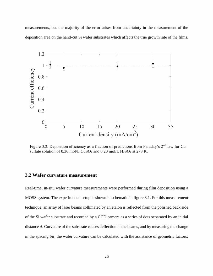
measurements, but the majority of the error arises from uncertainty in the measurement of the
deposition area on the hand-cut Si wafer substrates which affects the true growth rate of the films.
3.2 Wafer curvature measurement
Real-time, in-situ wafer curvature measurements were performed during film deposition using a
MOSS system. The experimental setup is shown in schematic in figure 3.1. For this measurement
technique, an array of laser beams collimated by an etalon is reflected from the polished back side
of the Si wafer substrate and recorded by a CCD camera as a series of dots separated by an initial
distance 𝑑. Curvature of the substrate causes deflection in the beams, and by measuring the change
in the spacing 𝛿𝑑, the wafer curvature can be calculated with the assistance of geometric factors:
Figure 3.2. Deposition efficiency as a fraction of predictions from Faraday’s 2nd law for Cu
sulfate solution of 0.36 mol/L CuSO4 and 0.20 mol/L H2SO4 at 273 K.
.

27
𝜅 =1
𝑟=
𝛿𝑑
𝑑
𝑐𝑜𝑠𝛼
2𝐿, (3.3)
where 𝑟 is the radius of curvature, 𝐿 is the distance between the camera and the film, and 𝛼 is the
angle of incidence of the laser beams. The average stress in the film and the stress thickness can
be calculated from the curvature with the Stoney equation as discussed in chapter 2.
An example of a stress thickness vs thickness plot calculated from wafer curvature measurements
is shown in figure 3.3. For this film, growth was interspersed with periods of no growth.
Measurements were taken continuously over time, as shown in the inset, but control of the growth
rate and deposition time permit the construction of a plot vs film thickness. Measurement of the
Figure 3.3. Stress thickness vs thickness of Cu film electrodeposited at 0.96 nm/s with periods
of paused growth. Vertical dotted lines indicate pauses. Inset: Stress thickness vs time for a
segment of the deposition with the periods of paused growth highlighted in grey.
.

28
slope of a stress thickness vs thickness plot provides the instantaneous stress at the film height
chosen. When the slope is linear, the film has reached steady state growth. The error in stress
measurement for the MOSS system is less than 1 MPa when calibrated correctly.
3.3 Grain size measurement
Microstructure of the deposited copper films was investigated by taking several FIB cross-sections
of each film. The film surface was protected by a sputtered layer of Pt to minimize erosion damage
while the viewing trench was excavated and the cross-section cleaned. A typical cross-section of
electrodeposited Cu is shown in figure 3.4. Ga ion channeling results in different levels of
saturation in the micrographs for grains of different orientations, which enables identification of
grain boundaries. The microstructure of electrodeposited copper is typically characterized by grain
Figure 3.4. a) Electrodeposited Cu with unannealed seed layer, showing grains of increasing
size, with an example line of intercepts such as those used to calculate average grain size. b)
Cu with annealed seed layer and stable grain size.

29
size that steadily increases on average with the thickness of the film, from a few hundred
nanometers near the substrate to more than a micron at the surface, resulting in roughly V-shaped
grains, as in 3.4 a. A notable exception can occur if the seed layer was annealed; then, the average
grain size is more stable, though grains are only roughly columnar, as shown in 3.4 b.
Grain size was measured using the lineal intercept method outlined in ASTM standard E112-12
[2], with the factor of 4/𝜋 applied to relate the measured intercept length to grain diameter for
grains approximately circular in the plane of the film. 5-7 different cross-section images were
analyzed for each film in order to provide a representative sampling. An example line with
intercepts is included in 3.4 a). Twin boundaries were not counted for the purpose of this research,
because they do not form a typical triple junction with the surface of the film; there is no meeting
of two distinct layers to generate Hoffman stress, and atomic insertion and mobility is limited
because the boundary region is not disordered. For depositions where the growth rate of the film
was well known, any particular thickness or height level of the film can be correlated with the time
of the deposition and the instantaneous stress in the film. Therefore, in situations where the grain
size is unlikely to change significantly during further deposition or before the sample can be cross-
sectioned with the FIB, the grain size, growth rate, and instantaneous stress can be found for each
point in time.
3.4 Fitting routines
The kinetic model presented in chapter 2 was fit to experimental data using programs written in
Matlab. The purpose of this fitting was to find values for the smallest number of variables needed
to match the behavior of a set of data or several sets of data with the numerically integrated form

30
of the model. How well the model can describe and predict the relationship of the stress to the
known deposition parameters provides support for the underlying physical assumptions of atomic
mobility and stress generation that the model is based on. Ultimately, kinetic parameters for
different materials or deposition systems may provide insight into fundamental system
characteristics.
The programs written were designed to minimize the function of the difference between the data
measured and the values calculated by the model. By varying the parameters which contribute to
the model calculation, the program finds the closest fit between the data and the model predictions.
Parameters like 𝜎𝐶, 𝜎𝑇, or 𝛽𝐷 can be fit to find unique values for different subsets of the data or
singular values for all data sets being fit. Initial values are provided for parameters being fit, as
well as lower and upper bounds. In cases where 𝛽𝐷 was permitted to vary, it did so in two ways.
First, a central 𝛽𝐷 value was allowed to vary within a range provided. Then, a second, smaller
variation was permitted around the central value. With this method, parameter values can vary
only slightly from each other yet still find an optimal value significantly removed from the initial
value provided.
The fitting procedure used a trust-region-reflective least squares algorithm [3]. This routine makes
use of an iterative process which generates a function simpler than the complete function being
minimized, but with similar behavior over a small local region: the trust region. Each attempted
step is then a minimization over the trust region. A step attempt fails if the new variables resulting
from the minimization lead to a higher value for the function, and the trust region is reduced until
a good approximation and minimization can be made. The process then iterates until a local
minimum is found or the step size is sufficiently small, following the same process each iteration
31
of generating a local approximation for the function, identifying a trust region, and attempting a
step. Fitting routines were allowed to run until convergence, when a stable function value emerged.
The results of this fitting process are presented in following chapters. Specific program samples
can be found in Appendix A.
References
[1] J. W. Shin, "Stress generation and relaxation in thin films: the role of kinetics and grain
boundaries," Ph.D. thesis, School of Engineering, Brown University, 2009.
[2] ASTM Standard E112-12: Test Methods for Determining Average Grain Size, ASTM
International, 2012.
[3] “Least-Squares (Model Fitting) Algorithms - MATLAB & Simulink.” Documentation,
MathWorks, 2017, www.mathworks.com/help/optim/ug/least-squares-model-fitting-
algorithms.html.

32
Chapter 4
Patterned Films
This chapter explores several sets of experiments with metal films electrodeposited onto
photolithographically patterned substrates with continuous wafer curvature measurement during
deposition. Two types of patterning will be discussed: square arrays of hemispherical metal islands
with two-dimensional (2D) symmetry, presented in section 4.1, and arrays of parallel channels
which lead to the growth of parallel semicylinders with one-dimensional (1D) symmetry, in section
4.2. Stress thickness data collected by the groups who performed the deposition experiments were
used to test the kinetic model described in chapter 2 against systems with well-defined geometry
and known growth parameters undergoing a controlled process of island coalescence.
4.1 2D symmetry
4.1.1 Experiment
The first set of experiments, Ni electrodeposited on substrates with a square array of vias, were
performed by Sean Hearne at Sandia National Laboratory [1]. Samples were fabricated from (001)
Si wafer substrates 100 μm thick with a multilayer structure shown in Figure 4.1. 100 m Si was
coated with 15 nm of evaporated Ti and 150 nm of evaporated Au, then covered with
approximately 1.3 μm of photoresist. The photoresist was lithographically patterned with a square
array of vias 2.2 μm in diameter and 22 μm apart. Onto this multilayer structure, Ni films were
deposited from a sulfamate solution with 1.36 mol/L of Ni and 0.81 mol/L of boric acid

33
held at 50 °C, first conditioned for 4 hours at 10 mA/cm2 prior to deposition for the removal of
trace ionic contaminants and de-aerated by bubbling ultra high purity nitrogen gas for at least 24
hours. The reference electrode was a Mercury-Mercury sulfate reference electrode (MSE)
saturated with K2SO4. Electrodeposition was performed using potentiostatic control, that is, at
constant voltage, so that the radius of the islands, 𝜌, increased at a constant rate R regardless of the
deposition area of the highly non-uniform film. The narrow vias through the photoresist to the
conductive layer beneath provided the only deposition surface for metal ions leaving the solution,
so Ni first filled the vias, then formed uniform hemispherical islands centered on each via. SEM
micrographs of these films before, during, and after island coalescence are shown in figure 4.2.
The uniform size, shape, and spacing of the islands ensured that when coalescence began, contact
was initiated near-simultaneously between all adjacent islands across the film. The shape of these
islands as they coalesce became increasingly complex, as demonstrated in figure 4.3. Each island
had a square footprint in which to expand, so as the radius of the islands increased, as measured
from the top of the via to the curved surface of the film, the shape evolved from a
Si: 100 m
L=22 m
Ni Ni
Ti: 15 nm
Au: 150 nm
P.R.: ~1.3 μm
Figure 4.1. Schematic cross-section of the multilayer structure used for 2D-symmetric
electrodeposition of Ni.

34
Figure 4.2. (a)-(c) Plane view SEM micrographs of patterned Ni films grown for 5400s to a
radius of 9.9 μm, 6270s to a radius of 11.9 μm, and 7550s to a radius of 14.5 μm, respectively.
(d)-(f) Cross-sections of the islands pictured in (a)-(c), correlating with the images above.
11 m 11 m 11 m
a) b) c)
d) e) f)
22 m 22 m 22 m
Figure 4.3. Schematic demonstrating three stages in the evolution of the geometry of
hemispherical islands growing in a LxL square grid. The radius of the island is 𝜌 and the radius
of the face is 𝑟. a) Prior to coalescence, the island is hemispherical in shape, and 𝜌 < 𝐿/2. b)
When 𝐿
2< 𝜌 < ξ𝐿, flat semicircular faces form at the contact area between islands. c) At 𝜌 >
ξ𝐿, the island is a hemisphere truncated to a square base, and the contact areas are rectangles
with curved top edges.

35
simple hemisphere to a hemisphere with truncated sides. There are three distinct stages of island
coalescence. Initially, islands are hemispherical. Next, after the first instant of coalescence at
radius 𝜌 > 𝐿/2, islands are truncated hemispheres with four flat faces shaped like semicircles.
Finally, after the radius of the island has increased to 𝜌 > ξ𝐿, the substrate is fully covered, and
the flat sides of each island meet at the corners to form rectangles with curved top edges.
Radial growth rate 𝜌 for each deposition was determined by fitting the thickness derived from the
Faradic current and corrected for deposition efficiency by SEM measurements of island size to a
calculated island volume, as shown in Figure 4.4. An offset in deposition time was allowed to
account for the difference between an idealized hemisphere grown from a point and the reality of
Figure 4.4. Thickness data for each deposition (solid lines) paired with calculated island
volumes (dashed lines). Deposition voltages of -1.39, -1.35, -1.32, -1.31, and -1.29 V were
found to produce constant radial growth rates of 2.0, 2.9, 3.3, 4.1, and 5.1 nm/s respectively.

36
the islands first growing as posts. To translate from island volume to average thickness, a factor
was applied of 1/𝐿2. There is overall good agreement between the calculated and measured
thickness, especially post-coalescence. The thickness during coalescence was slightly higher than
expected for an idealized volume; this may be due to some slight deviation in the surface, shape,
or uniformity of the islands. Deposition voltages of -1.39, -1.35, -1.32, -1.31, and -1.29 V were
found to produce constant radial growth rates of 2.0, 2.9, 3.3, 4.1, and 5.1 nm/s respectively, with
time offsets of 1692, 1056, 1107, 926, 925. Similar time offsets were allowed between the actual
time of coalescence and the calculated ideal in fitting the data to the kinetic model as described
next.
4.1.2 Model fitting
The kinetic model laid out in chapter 2 relies on the fundamental mechanisms of tensile stress
generation arising from adjacent grain coalescence to generate new grain boundary area and
compressive stress resulting from surface adatoms being inserted into the newly formed grain
boundary. For the purposes of applying this triple junction stress model to patterned films, the
contact areas between islands are treated as the only relevant grain boundaries, despite each
individual island being comprised of many internal grains, as is visible in figure 4.2. The enforced
length scale of the patterning means that the boundaries between islands function as analogous to
the boundary between randomly nucleated single grains in a stochastic film. The contribution of
the internal grain boundaries to the total stress in the film, if any, is ignored for this application of
the model to these patterned films. As there is little to no stress measured prior to island
coalescence, this simplification is reasonable until the point at which a film approaches uniformity

37
and the more marked boundaries between islands are subsumed. Experimental data and the results
of model fitting with the growth rates found by volumetric fitting are shown in figure 4.5. A fit to
the model with radial growth rates determined by a linear fit to the approximately steady-state
behavior of each film well past the point of coalescence was previously published in [1]. The fits
are just as good with growth rates from either method; the difference is essentially proportional,
as shown in figure 4.6. The well-defined shape of the islands as they evolve through the stages
shown in figure 4.3 allows the area of contact between the island ‘grains’ and the increase in ‘grain
boundary’ or contact area 𝐴 to be calculated precisely, and therefore the grain boundary velocity
Figure 4.5. Stress thickness data measured by wafer curvature for the deposition of Ni at several
growth rates, as indicated on the figure. Solid blue lines are the result of stress model fit discussed
in the text.
4.1 nm/s
5.1 nm/s
3.3 nm/s
2.9 nm/s
2.0 nm/s

38
𝜕ℎ𝑔𝑏
𝜕𝑡 can be calculated as well. With this geometry,
𝜕ℎ𝑔𝑏
𝜕𝑡 is the same as the rate of increase of the
radius of the contact face of the islands, 𝜕𝑟
𝜕𝑡. In the earliest stages of hemispherical islands impinging
on one another, small changes in the radius of the islands create large changes in the contact area.
Thus, the grain boundary velocity is 0 before a boundary forms between islands but reaches its
maximum value at the first instant of coalescence. As the islands grow, their curvature becomes
less extreme, and grain boundary velocity decreases over time until it reaches a steady state value,
Figure 4.6. Growth rates found by volumetric fitting vs. growth rates found by linear approximation
from the steady state.

39
dependent on the growth rate, as the film becomes uniform. The calculated grain boundary
velocities for the fits shown in figure 4.5 are shown in figure 4.7.
Knowing the value of the grain boundary velocity at each stage of the deposition permits the use
of the following expression for the stress in each layer of the film 𝜎𝑖, a combination of equations
2.12 and 2.15:
𝜎𝑖 = 𝜎𝐶 + (𝜎𝑇 − 𝜎𝐶)𝑒(−
𝛽𝐷𝐿
1
𝑑𝑟𝑑𝑡
)
, (4.1)
where 𝜎𝐶 is the compressive stress parameter, 𝜎𝑇 is the tensile stress parameter, 𝛽𝐷 is the
parameter for kinetic and material constants, and L is 22 μm. The grain boundary velocity, here
𝑑𝑟
𝑑𝑡, is related to the constantly increasing radius of the islands 𝜌 such that
4.1 nm/s
5.1 nm/s
3.3 nm/s
2.9 nm/s
2.0 nm/s
Figure 4.7. Grain boundary velocity over time for hemispherical islands in a square array with radial
growth rates as indicated in the figure.
40
𝑑𝑟
𝑑𝑡=
𝑑𝜌
𝑑𝑡
𝜌
√𝜌2 −𝐿2
4
. (4.2)
Direct comparison between the model and the experiments requires a numerical integration of the
stress thickness [1],
⟨𝜎(𝑡)⟩ℎ𝑎𝑣𝑔(𝑡) =1
𝐿∫ ∫ 𝜎(𝑟(𝜏))
𝑡
0
𝜕𝐴
𝜕𝜏𝑑𝜏, (4.3)
with the contact area 𝐴 between islands defined as
for 𝑟 <𝐿
2: 𝐴 =
1
2𝜋𝑟2 (4.4)
when the faces are semicircular, then
for 𝑟 >𝐿
2: 𝐴 = 𝑟2 sin−1 (
𝐿
2𝑟) +
𝐿√𝑟2 −𝐿2
42
(4.5)
afterward. It is important to note that the geometry contributes to the stress thickness in two ways:
in the rate of change of the border of the contact area key to the calculation of the stress, and with
the change in contact area determining the extent to which that stress is applied.
With well-defined geometry providing values for 𝐿, 𝑑𝑟
𝑑𝑡, and
𝑑𝐴
𝑑𝑡, the parameters that needed to be
determined for equations 4.1 and 4.3 to describe experimental results directly were 𝜎𝐶, 𝜎𝑇, and
𝛽𝐷. A non-linear least squares fitting routine was used to minimize the difference between the
stress thickness determined from wafer curvature measurements and the values calculated by the
model. Common values for 𝜎𝐶 and 𝜎𝑇 were shared between all data sets, while values for 𝛽𝐷 were
allowed to vary slightly between data sets in order to account for the possibility of discrepancies

41
in the experimental conditions. There was also an offset applied to the deposition time in the
calculation of island radius to compensate for the fact that before islands became hemispherical,
deposited Ni had to fill the cylindrical vias in the photoresist. This offset allowed the predicted
time for the onset of coalescence to correlate with the increase in tensile stress seen in figure 4.5.
Values found for the fit shown in figure 4.5 are presented in table 4.1.
V R (nm/s) L (μm) 𝝈𝑪 (MPa) 𝝈𝑻 (MPa) 𝜷𝑫 (nm2/s)
-1.39 5.1 22 -187.5 42.42 57700
-1.35 4.1 - - - 56900
-1.32 3.3 - - - 58100
-1.31 2.9 - - - 58000
-1.29 2.0 - - - 56000
4.2 1D symmetry
4.2.1 Experiment
The next set of experiments was performed and first published by Bhandari [2], following the
format first presented by Hearne in [3]. The films deposited were characterized by a distinct
geometry with one-dimensional symmetry, parallel trenches in patterned photoresist which
developed into parallel hemicylinders with Ni electrodeposition. The spacing between the
trenches, and thus the ultimate size of the shaped islands, was set to L=26.5, 10.6, or 5.6 μm from
Table 4.1. 2D patterned film kinetic model fitting parameters for electrodeposited Ni.

42
center to center. The width of the trenches was a constant ratio of 2.65, resulting in trenches of
width 10, 4, and 2.11 μm, respectively. After deposited Ni filled the rectangular trenches to the
level of the height of the photoresist, the resulting islands became axially symmetric semicylinders
which formed contact surfaces shaped like simple rectangles between adjacent islands. A sketch
and sample cross-section to show the film structure are shown in figure 4.8.
The films in this chapter were deposited under potentiostatic conditions to ensure constant radial
island growth. The multilayer structure of the substrate was 100 μm Si (001), 15 nm evaporated
Ti, 150 nm evaporated Au, and the patterned photoresist. The electrodeposition solution was
Figure 4.8. Cross section and sketch of a patterned electroplated Ni on Au
L
Ni
Substrate

43
comprised of 1.36 mol/l nickel sulphamate and 0.72 mol/l boric acid, held at 40 °C. It was
conditioned to remove trace contaminates for 4 hours at 10 mA/cm2, then bubbled with N2 gas for
24 hours to remove O2. The bath was continuously maintained with constant N2 bubbling and
pumping through a 0.5 μm filter. Reported growth rates ranged from 0.32 to 5.33 nm/s, with
estimates from the total charge exchanged during deposition corrected for deposition inefficiency
using SEM cross-section measurements of island size [2].
4.2.2 Curvature measurement interpretation
Films deposited on patterned substrates with less than biaxial symmetry face unique difficulties in
relating the measured curvature to the directional stress in the film [4]. Complications also arise
for these particular films from the proportionally significant area of the seed layer exposed in the
trenches. Additionally, Stoney’s equation assumes that the thickness of the film is small compared
to the thickness of the substrate; for films with significant proportional thickness, such as those
analyzed here, a correction factor must be applied.
For the highly asymmetric semicylindrical islands, care must be taken when relating the curvature
measured to stress in the film. The modified Stoney’s equation used, formulated for anisotropic
films with curvature measured along the x-axis, 𝜅𝑥, was described in [5]:
𝜅𝑥 =6(𝑓𝑥 − 𝜈𝑆𝑓𝑦)
𝐸𝑆ℎ𝑆2 , (4.6)
where 𝐸𝑆 is the elastic modulus, ℎ𝑆 is the thickness, and 𝜈𝑆 is the Poisson’s ratio of the substrate.
The factors 𝑓𝑥 and 𝑓𝑦 are contributions to the stress thickness in the x- and y- direction; in a uniform
or symmetric film, they are equal. The x direction is defined here as being the direction of radial

44
growth for the islands. The plane normal to the x direction is parallel to the rectangular contact
area between adjacent islands, at 𝑥 = ±𝐿/2 from the island center, with the height of the contact
area noted as the height of the ‘grain boundary,’ ℎ𝑔𝑏. The y direction is along the trench, and z is
normal to the substrate. A schematic is shown in figure 4.9.
The forces 𝑓𝑥 and 𝑓𝑦 can be found by integrating the stress in each direction over the relevant area,
as first presented in [6]. For the x-direction, 𝑓𝑥, the stress thickness contribution is a product of the
contact area between islands and the stress normal to it:
𝑓𝑥 = ⟨𝜎𝑥𝑥⟩ℎ𝑓 = ∫ 𝜎𝑥𝑥 (𝑥 =𝐿
2, 𝑧) 𝑑𝑧, (4.7)
ℎ𝑔𝑏
0
with ⟨𝜎𝑥𝑥⟩ defined as the average stress normal to the x-direction and ℎ𝑓 being the average height
of the film. It then follows that 𝑓𝑦 can be described with the stress in the y-direction and the cross-
section of the islands:
Figure 4.9. Detailed schematic of semicylindrical island, post-coalesence.

45
𝑓𝑦 = ⟨𝜎𝑦𝑦⟩ℎ𝑓 =1
𝐿∫ ∫ 𝜎𝑦𝑦(𝑥, 𝑧)𝑑𝑥𝑑𝑧
𝐿/2
−𝐿/2
(4.8)∞
0
and ⟨𝜎𝑦𝑦⟩ is the average stress normal to the y-direction.
For films that are very thin relative to the substrate, it is appropriate to use Stoney’s equation for
uniform films or equation 4.6 for anisotropic films. However, for very thick films, the resistance
to curvature of the film itself must be taken into account. Freund et al developed a correction factor
for the measured curvature 𝜅𝑚𝑒𝑠 for uniform, isotropic films [7], but it was applied to the
anisotropic films here as in ref. [2]:
𝜅𝑚𝑒𝑠 = 𝜅𝑆𝑡𝑜𝑛𝑒𝑦 (1 +ℎ𝑓
ℎ𝑆) [1 + 4
ℎ𝑓
ℎ𝑆
𝐸𝑓
𝐸𝑆
+ 6ℎ𝑓
2
ℎ𝑆2
𝐸𝑓
𝐸𝑆
+ 4ℎ𝑓
3
ℎ𝑆3
𝐸𝑓
𝐸𝑆
+ℎ𝑓
4
ℎ𝑆4
𝐸𝑓2
𝐸𝑆2
]
−1
. (4.9)
The subscripts f and s are for the film and substrate, respectively, with h as the height and E the
plane strain modulus. 𝜅𝑆𝑡𝑜𝑛𝑒𝑦 is then the curvature that would be expected from a thin film. The
ratio of the plane strain moduli, 𝐸𝑓 𝐸𝑆
⁄ , was taken as 1.4.
The final complication arising from the geometry of these films lies in the photoresist trenches.
The area of exposed Au seed layer – 37.7% of the total area of the films – is large enough that the
nucleation and coalescence of stochastic Ni films at the start of film deposition has a detectable
contribution to the stress in some films. The data from curvature measurement as translated into
stress thickness over time is presented in figure 4.10 for three sets of island spacings, with 5-7
growth rates each. The initial tensile rise from randomly nucleated grains coalescing is most
obvious in 4.10 c), for island arrays of 26.5 µm spacing.

46
4.2.3 Fitting to kinetic model
The kinetic model detailed in chapter 2 was conceived to explain the stress development of uniform
polycrystalline films. The two fundamental mechanisms that generate stress during film deposition
are a Hoffman tensile stress from adjacent grains coming together and a compressive stress
generated at the triple junction from adatom insertion into the grain boundary. For patterned films,
the regularly spaced islands of enforced scale act as grains, and the contact area between these
islands is analogous to a grain boundary. The anisotropic formulation for relating film stress to
curvature is outlined in the previous section (equations 4.7-4.9), but accommodations must also be
made in adopting the standard kinetic model to these patterned films in accounting for stress
generated normal to the x- and y-directions. The stress thickness measured over time and the results
of model fitting to the data are shown in figure 4.10, with Ni films electrodeposited at 5-7 growth
rates each into parallel arrays that developed into semicylindrical islands with a) 5.3 b) 10.6 and
c) 26.5 μm spacing.
Stress at the boundaries between islands is only generated in the x-direction because the contact
areas are parallel to the yz plane, and these stresses are dominant. For stress measured along the
x-direction 𝜎𝑥𝑥, the stress in each layer becomes
𝜎𝑥𝑥,𝑖 = 𝜎𝐶 + (𝜎𝑇 − 𝜎𝐶,0)𝑒
−𝛽𝐷𝐿
1𝑑ℎ𝑔𝑏(𝑖)
𝑑𝑡 (4.10)
where 𝜎𝑇 is the characteristic tensile parameter expected to be proportional to 1/ξ𝐿, 𝛽𝐷 is the
parameter of material and kinetic constants that should be essentially uniform for all depositions
of similar material and conditions, and 𝑑ℎ𝑔𝑏(𝑖)
𝑑𝑡 is the rate of change of the height of the contact area,

47
Figure 4.10. Stress thickness vs thickness data (dots) and model fitting as described in text
(solid lines) for Ni films electrodeposited on patterned substrates of parallel trenches (1D
patterning) in arrays with a) 5.3 b) 10.6 and c) 26.5 μm spacing.

48
which changes as the geometry evolves as well as with deposition rate. The distinction between
𝜎𝐶 and 𝜎𝐶,0 here is an important one, which will be discussed shortly.
As similarly noted in 4.1.2 for hemispherical islands, in semicylindrical islands the grain boundary
velocity 𝑑ℎ𝑔𝑏
𝑑𝑡 changes as the island geometry evolves as well as with deposition rate. The
relationship between radial island growth and the grain boundary velocity is simpler for
semicylindrical islands than for hemispheres during coalescence, because the contact area is a
rectangle of constant width (the width of the substrate) and changing height. The area increases
most rapidly at the moment of first coalescence, when the angle between the two encroaching
surfaces is most acute. An illustration of the relationship between contact angle, grain boundary
velocity, and average height is shown in figure 4.11 a). This is the cause of the very sharp rises in
tensile stress at the onset of coalescence seen in figure 4.10; semicylinder coalescence generates
more immediate tensile stress that hemisphere coalescence because the area at first contact is much
larger. The grain boundary velocity decreases to approach 𝑅, the rate of increase of the radius 𝑟,
which as the film becomes uniform becomes the growth rate for the average height of the film ℎ,
𝜕ℎ𝑔𝑏
𝜕𝑡
L
a) b)
ℎ
ℎ/𝐿
Figure 4.11. a) Illustration of the evolving relationship between the grain boundary velocity,
average height, and radius of coalescing islands of semicircular cross-section as deposition
progresses. b) Generalized plot of grain boundary velocity with film thickness.
49
as shown in 4.11 b). Because the geometry of the patterned films is well defined, once the islands
have made contact at 𝑟 > 𝐿/2, the grain boundary velocity can be calculated as
𝑑ℎ𝑔𝑏(𝑖)
𝑑𝑡=
𝑅 ∙ 𝑟(𝑖)
√𝑟(𝑖)2 −𝐿2
4
, (4.11)
where 𝐿 is again the pattern spacing.
This contact between the islands in the x-direction generates the bulk of the stress measured during
film deposition, but not all. A complication to the 1D patterned films that must be accounted for
is the additional effect of stress in the y-direction, along the length of the islands. This is done with
a slight change to the typical parameter 𝜎𝐶 for compressive stress, which is instead defined as:
𝜎𝐶 = 𝜎𝐶,0 − 𝜎𝑦𝑦,𝑆𝑆 (4.12)
𝜎𝐶,0 here is the standard stress due to adatom jumps into the grain boundary driven by
supersaturation, and 𝜎𝑦𝑦,𝑆𝑆 is the steady state contribution of stress generated in the y-direction.
The steady state is assumed because coalescence of the randomly nucleated islands is expected to
resolve rapidly. This considerably simplifies the expression for 𝑓𝑦 = ⟨𝜎𝑦𝑦⟩ℎ𝑓 as defined in
Equation 4.8. With the average stress ⟨𝜎𝑦𝑦⟩ approximated as uniform, 𝑓𝑦 then changes only with
the thickness of the film, and 𝜎𝑦𝑦,𝑆𝑆 can be treated as a fitting parameter unique to each deposition.
As outlined in Equation 4.6, the y-direction contribution to the curvature is proportional to −𝜈𝑆,
with 𝜈𝑆 for Si taken as 0.278. Note that in the y-direction there are no gaps between trenches to be
overcome, so stress is generated well before the semicylindrical islands begin to coalesce and
continues afterward. Although the stress appears compressive prior to semicylinder contact, the
force in the y-direction is generally tensile and follows the same trends typical for steady state
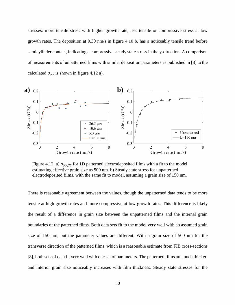
50
stresses: more tensile stress with higher growth rate, less tensile or compressive stress at low
growth rates. The deposition at 0.30 nm/s in figure 4.10 b. has a noticeably tensile trend before
semicylinder contact, indicating a compressive steady state stress in the y-direction. A comparison
of measurements of unpatterned films with similar deposition parameters as published in [8] to the
calculated 𝜎𝑦𝑦 is shown in figure 4.12 a).
There is reasonable agreement between the values, though the unpatterned data tends to be more
tensile at high growth rates and more compressive at low growth rates. This difference is likely
the result of a difference in grain size between the unpatterned films and the internal grain
boundaries of the patterned films. Both data sets fit to the model very well with an assumed grain
size of 150 nm, but the parameter values are different. With a grain size of 500 nm for the
transverse direction of the patterned films, which is a reasonable estimate from FIB cross-sections
[8], both sets of data fit very well with one set of parameters. The patterned films are much thicker,
and interior grain size noticeably increases with film thickness. Steady state stresses for the
Figure 4.12. a) 𝜎𝑦𝑦,𝑆𝑆 for 1D patterned electrodeposited films with a fit to the model
estimating effective grain size as 500 nm. b) Steady state stress for unpatterned
electrodeposited films, with the same fit to model, assuming a grain size of 150 nm.
a) b)

51
patterned films were linear fits to the thickest part of each film. The parameter values for all fits to
the steady state model are presented in table 4.2.
There is no significant trend in 𝜎𝑦𝑦,𝑆𝑆 with the island spacing, which is to be expected; 𝜎𝑦𝑦,𝑆𝑆 does
not change with the width of the trenches or the film height at semicylinder coalescence. In
contrast, the steady state stresses of the complete films are highly dependent on pattern spacing,
as shown in figure 4.13.
The fits shown in figures 4.12 and 4.13 enforce a 1/ξ𝐿 dependence for 𝜎𝑇, as predicted by the
Hoffman model. By finding a separate value of 𝜎𝑇 for each pattern spacing 𝐿, we can test this
assumption. Figure 4.14 shows that the tensile stress parameters calculated follow the expected
Hoffman scaling well, though the range covered by the patterned films is narrow enough that other
disconnect is due to the very large difference in grain size, a subtle effect of geometry, or the
simple likelihood that the patterned film depositions were not carried out far enough past the point
of coalescence to a true steady state.
L (μm) 𝝈𝑪,𝟎 (MPa) 𝝈𝑻 (MPa) 𝜷𝑫 (nm2/s)
0.150 -248.7 153.9 58
0.500 - 84.3 -
5.3 -11.5 152.0 7850.4
10.6 - 107.5 -
26.5 - 67.9 -
Table 4.2. Steady state 1D patterned kinetic model fit parameters for electrodeposited Ni.

52
5.3 µm
10.6 µm
26.5 µm
Figure 4.13. Steady state total stress measured for 1D patterned films. Solid lines are fit
to model assuming 𝜎𝑇 ∝ 1/ξ𝐿 with 𝐿 as the pattern spacing.
Figure 4.14. Fitted steady state tensile parameters for patterned 1D films, fitted to a line with
1/ξ𝐿 dependence.
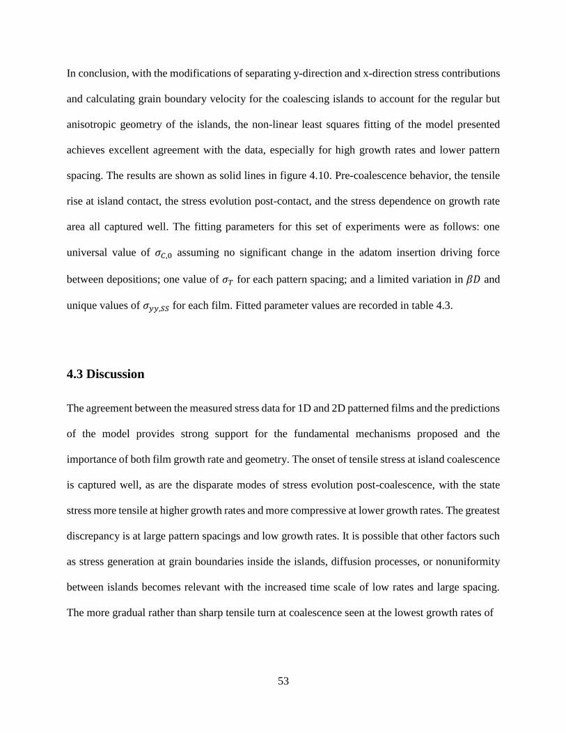
53
In conclusion, with the modifications of separating y-direction and x-direction stress contributions
and calculating grain boundary velocity for the coalescing islands to account for the regular but
anisotropic geometry of the islands, the non-linear least squares fitting of the model presented
achieves excellent agreement with the data, especially for high growth rates and lower pattern
spacing. The results are shown as solid lines in figure 4.10. Pre-coalescence behavior, the tensile
rise at island contact, the stress evolution post-contact, and the stress dependence on growth rate
area all captured well. The fitting parameters for this set of experiments were as follows: one
universal value of 𝜎𝐶,0 assuming no significant change in the adatom insertion driving force
between depositions; one value of 𝜎𝑇 for each pattern spacing; and a limited variation in 𝛽𝐷 and
unique values of 𝜎𝑦𝑦,𝑆𝑆 for each film. Fitted parameter values are recorded in table 4.3.
4.3 Discussion
The agreement between the measured stress data for 1D and 2D patterned films and the predictions
of the model provides strong support for the fundamental mechanisms proposed and the
importance of both film growth rate and geometry. The onset of tensile stress at island coalescence
is captured well, as are the disparate modes of stress evolution post-coalescence, with the state
stress more tensile at higher growth rates and more compressive at lower growth rates. The greatest
discrepancy is at large pattern spacings and low growth rates. It is possible that other factors such
as stress generation at grain boundaries inside the islands, diffusion processes, or nonuniformity
between islands becomes relevant with the increased time scale of low rates and large spacing.
The more gradual rather than sharp tensile turn at coalescence seen at the lowest growth rates of
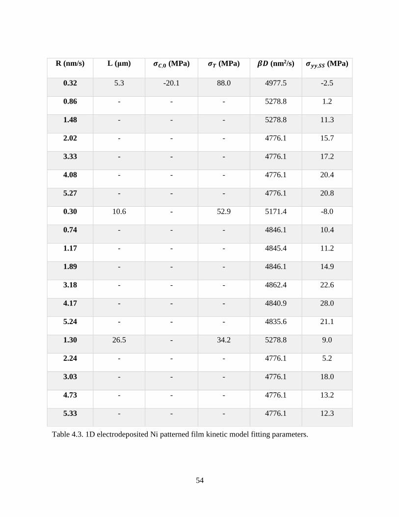
54
R (nm/s) L (μm) 𝝈𝑪,𝟎 (MPa) 𝝈𝑻 (MPa) 𝜷𝑫 (nm2/s) 𝝈𝒚𝒚,𝑺𝑺 (MPa)
0.32 5.3 -20.1 88.0 4977.5 -2.5
0.86 - - - 5278.8 1.2
1.48 - - - 5278.8 11.3
2.02 - - - 4776.1 15.7
3.33 - - - 4776.1 17.2
4.08 - - - 4776.1 20.4
5.27 - - - 4776.1 20.8
0.30 10.6 - 52.9 5171.4 -8.0
0.74 - - - 4846.1 10.4
1.17 - - - 4845.4 11.2
1.89 - - - 4846.1 14.9
3.18 - - - 4862.4 22.6
4.17 - - - 4840.9 28.0
5.24 - - - 4835.6 21.1
1.30 26.5 - 34.2 5278.8 9.0
2.24 - - - 4776.1 5.2
3.03 - - - 4776.1 18.0
4.73 - - - 4776.1 13.2
5.33 - - - 4776.1 12.3
Table 4.3. 1D electrodeposited Ni patterned film kinetic model fitting parameters.
55
the data in figure 4.10 b) and c) most likely indicates uneven growth slightly scattering the time of
first contact.
One fundamental assumption made is that the stresses across the nonuniform contact areas between
islands generate substrate curvature that can be accurately interpreted by Stoney’s equation, which
itself assumes uniform stresses over a uniform film. To some extent, even the assumption that
nonuniform stress can be measured accurately is unproven. In the case of coalescing films in
general, the highly nonuniform nature of the film and the large proportion of free surfaces may
interfere with stress in the deposited layers being translated into substrate curvature. In the case of
the coalescing hemispherical arrays, the problem is more similar to the distribution of stress along
a mesh, with regularly spaced voids between continuous symmetrical lines. Finite element analysis
is currently in progress to determine the extent of the effect of these internal free surfaces, if any.
4.4 Volmer-Weber film fit with 2D model
The framework for hemispherical island coalescence described in section 4.1 assumes a square
array of uniform islands, but the geometry should in general approximate the behavior of a
randomly nucleated film that forms on a substrate as isolated islands with near-uniform grain size,
a Volmer-Weber film. The primary difference between the patterned and unpatterned film is the
statistically distributed time of initial contact between islands unlike the simultaneous coalescence
across the film seen with islands of uniform size and spacing. Therefore, a fit to the kinetic model
formulated for hemispherical islands described in 4.1.2 would not be expected to capture the exact
coalescence behavior of a randomly nucleated film, but could otherwise describe stress evolution
and general trends. A fit to a series of depositions of randomly nucleated Volmer-Weber thin films

56
of silver evaporated at 0.2 nm/s on to oxidized Si substrates at a range of temperatures [9, 10] is
presented in figure 4.15, with fitted parameter values in table 4.4. For depositions performed at
193-303 K, the model captures the relative height of the tensile rise of each film as it coaleseces
and describes the change in steady state behavior with temperature: as temperature increases, the
post-coalesence stress becomes less tensile, or more compressive. Depositions at 193-303 K can
be fit well to the model as described with equation in 4.1 with one value of 𝜎𝐶, one value of 𝜎𝑇,
and independent values of kinetic parameter 𝛽𝐷, as in the table below. The grain size 𝐿 was
estimated as 70 nm from TEM micrographs [9], which may be an incomplete picture with serious
ramifications, the consequences of which will be discussed shortly.
Figure 4.15. Stress thickness of evaporated Ag deposited at 0.2 nm/s and a range of
temperatures as indicated on figure. Dark lines are a fit to the hemispherical (2D) kinetic model
with parameters presented in table 4.4.

57
The kinetic parameter 𝛽𝐷 is expected to relate to temperature by
𝛽𝐷 =𝛽0𝐷0
𝑘𝐵𝑇𝑒
−𝐸𝑎
𝑘𝐵𝑇, (4.13)
where 𝑘𝐵 is the Boltzmann constant and 𝐸𝑎 is the activation energy for an atom jumping into the
grain boundary from the surface. Equation 4.13 can be rearranged to
ln(𝛽𝐷 𝑇) = −−𝐸𝑎
𝑘𝐵𝑇+ ln (
𝛽0𝐷0
𝑘𝐵), (4.14)
which shows that 𝐸𝑎 may be found by plotting ln(𝛽𝐷 𝑇) against 1/𝑘𝐵𝑇 and taking the linear slope,
as shown in figure 4.16. The activation energy for Ag deposition at 0.2 nm/s from the 𝛽𝐷 values
in table 4.4 is 0.112 eV.
T (K) L (nm) 𝝈𝑪 (MPa) 𝝈𝑻 (MPa) 𝜷𝑫 (nm2/s)
193 70 -67.8 92.2 0.090
223 - - - 0.137
238 - - - 0.187
253 - - - 0.215
303 - - - 0.226
323 - - - 0.260
373 - - - 0.292
Table 4.4. 2D patterned film kinetic model fitting parameters for evaporated Ag.
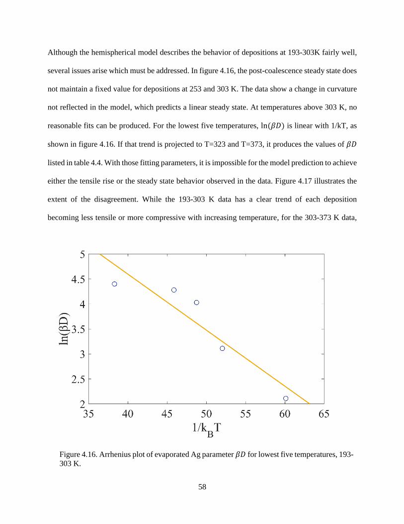
58
Although the hemispherical model describes the behavior of depositions at 193-303K fairly well,
several issues arise which must be addressed. In figure 4.16, the post-coalescence steady state does
not maintain a fixed value for depositions at 253 and 303 K. The data show a change in curvature
not reflected in the model, which predicts a linear steady state. At temperatures above 303 K, no
reasonable fits can be produced. For the lowest five temperatures, ln(𝛽𝐷) is linear with 1/kT, as
shown in figure 4.16. If that trend is projected to T=323 and T=373, it produces the values of 𝛽𝐷
listed in table 4.4. With those fitting parameters, it is impossible for the model prediction to achieve
either the tensile rise or the steady state behavior observed in the data. Figure 4.17 illustrates the
extent of the disagreement. While the 193-303 K data has a clear trend of each deposition
becoming less tensile or more compressive with increasing temperature, for the 303-373 K data,
Figure 4.16. Arrhenius plot of evaporated Ag parameter 𝛽𝐷 for lowest five temperatures, 193-
303 K.

59
the opposite trend is in evidence: both the steady state stress and the total stress in the film at film
heights of 100 nm become more tensile, or less compressive, with higher temperature.
Both of these issues, the non-linear steady state stresses as film thickness increases and the failure
of the model to predict the behavior of the data at high temperature, are most likely rooted in the
same cause. In the absence of grain size measurements for each temperature, the fits in figure 4.15
and table 4.4 reflect the assumption that the grain size is similar for each deposition and static over
time. However, this assumption is probably not valid. It is very likely that the behavior at 253 K
and higher where the post-coalescence stress becomes less compressive as thickness increases is
Figure 4.17. Evaporated Ag deposited at 0.2 nm/s and a range of temperatures. Dark lines for
323 and 373 K are drawn with parameters extrapolated from those of lower temperature fits,
while the thin lines are experimental data.

60
due to a tensile stress contribution arising from grain growth, which causes densification of the
film through the removal of grain boundaries. This is evidence that for unpatterned films, the role
of grain size and microstructure evolution cannot be ignored. Grain size measurement and control,
and the effects on stress evolution, will be a focus of the following chapters.
References
[1] E. Chason, J. Shin, C.-H. Chen, A. Engwall, C. Miller, S. Hearne and L. Freund, Journal
of Applied Physics 115 (12), 123519 (2014).
[2] A. Bhandari, B. W. Sheldon and S. J. Hearne, Journal of applied physics 101 (3), 033528
(2007).
[3] S. Hearne, S. Seel, J. Floro, C. Dyck, W. Fan and S. Brueck, Journal of applied physics 97
(8), 083530 (2005).
[4] A. J. Detor, A. M. Hodge, E. Chason, Y. Wang, H. Xu, M. Conyers, A. Nikroo and A.
Hamza, Acta materialia 57 (7), 2055-2065 (2009).
[5] L. B. Freund and S. Suresh, Thin film materials: stress, defect formation and surface
evolution. (Cambridge University Press, 2004).
[6] E. Chason, A. Engwall, C. Miller, C.-H. Chen, A. Bhandari, S. Soni, S. Hearne, L. Freund
and B. Sheldon, Scripta Materialia 97, 33-36 (2015).
[7] L. Freund, J. Floro and E. Chason, Applied Physics Letters 74 (14), 1987-1989 (1999).
[8] A. Bhandari, Brown University, 2007.
[9] S. C. Seel, C. V. Thompson, S. J. Hearne and J. A. Floro, Journal of Applied Physics 88
(12), 7079-7088 (2000).
[10] E. Chason, J. Shin, S. Hearne and L. Freund, Journal of Applied Physics 111 (8), 083520
(2012).

61
Chapter 5
The Effect of Microstructure on Stress in Thin Films
When considering how stress is generated in thin films during deposition, island morphology
during film coalescence cannot by itself explain how stress evolves in many films, especially past
the point of coalescence. The internal structure of these films must also be considered. This chapter
will discuss how changing grain size at the surface of a film or in the bulk can affect the stress as
a film is grown. First, a zone model of microstructural evolution will be described, categorizing
types of grain growth observed relative to atomic mobility. Then, experiments in systems with
behaviors characteristic of zones with low to moderate atomic mobility will be analyzed with
respect to the kinetic model for stress generation introduced in chapter 2.
5.1 Zone model of microstructure evolution
The zone model presented here characterizing thin film microstructure as a function of atomic
mobility is based on one first developed by Thornton [1] for sputtered thin films which considered
both substrate temperature relative to the melting point (T/Tm), and pressure of Ar. A version
broadly adapted for non-energetic deposition is represented as a schematic in Fig. 5.1. Three
distinct modes of microstructure evolution will be considered in this chapter. For the first and
simplest, zone I, a grain size established early in the deposition is maintained throughout the
thickness of the film. Grain sizes in zone I are generally but not always small; the final grain shapes
are columnar. Films with low atomic mobility typically display zone I behavior. In zone T, with

62
increased atomic mobility, grain size increases at the surface of the film as deposition progresses,
but material in the bulk of the film, below the surface, does not evolve. Zone T typically leads to
V-shaped grains, smaller at the base than at the surface. Finally, in zone II, the highest mobility of
these three, grain boundaries are mobile in the bulk of the film, and though grains are columnar,
the grain size increases in the previously deposited bulk of the film just as it does on the surface.
For zone I and zone T, the representative systems investigated are electroplated Ni and
electroplated Cu, respectively.
Figure 5.1. Schematic of grain structure changing with thickness for different regimes of atomic
mobility, adapted from Thornton [1].

63
In previously discussed versions of the kinetic model developed to describe the dependence of film
stress on growth rate and geometry, there were two primary mechanisms of stress generation:
tensile stress resulting from each new layer snapping together at the triple junction between two
adjacent grains and the film surface to form new segments of grain boundary, and compressive
stress from the insertion of adatoms from the surrounding film surface into the topmost layer of
that newly formed grain boundary. In the steady state for a uniform film, the rate of increase of the
height of the grain boundary is the same as the rate of increase for the average height of the film,
which is the deposition rate, R. When the grain size is constant, as in zone I, the stress in each layer
𝜎𝑖 is then:
𝜎𝑖 = 𝜎𝐶 + (𝜎𝑇 − 𝜎𝐶)𝑒(−
𝛽𝐷𝐿𝑅
), (5.1)
with 𝜎𝑇 and 𝜎𝐶 parameters for characteristic tensile and compressive stress respectively, 𝐿 the
constant grain size, 𝑅 the growth rate of the film, and 𝛽𝐷 the parameter for kinetic and material
constants. For zone T films where the grain size is changing at the surface, 𝐿 becomes 𝐿𝑖, subject
to change as the film grows. Note that equation 5.1 is only applicable to films where the stress in
each layer develops independent of previously deposited layers, that is, films where atomic
mobility is low enough that atom transport through the grain boundaries is negligible. The solution
for high mobility films will be discussed in the next chapter.
5.2 Electrodeposited Ni: Zone I
The first investigated system to be discussed is electrodeposited Ni, with a series of experiments
performed in collaboration with Zhaoxia Rao [2]. Films were grown under galvanostatic control
with a saturated calomel (SCE) reference electrode. The bath was comprised of 0.36 mol/L Ni
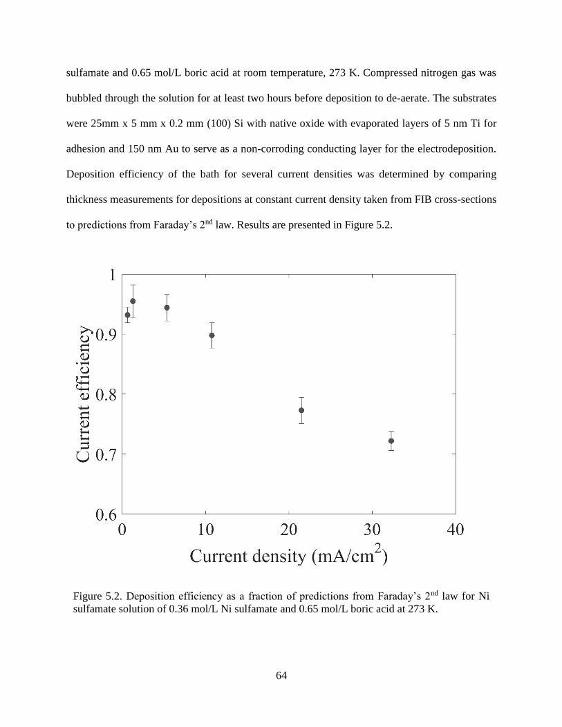
64
sulfamate and 0.65 mol/L boric acid at room temperature, 273 K. Compressed nitrogen gas was
bubbled through the solution for at least two hours before deposition to de-aerate. The substrates
were 25mm x 5 mm x 0.2 mm (100) Si with native oxide with evaporated layers of 5 nm Ti for
adhesion and 150 nm Au to serve as a non-corroding conducting layer for the electrodeposition.
Deposition efficiency of the bath for several current densities was determined by comparing
thickness measurements for depositions at constant current density taken from FIB cross-sections
to predictions from Faraday’s 2nd law. Results are presented in Figure 5.2.
Figure 5.2. Deposition efficiency as a fraction of predictions from Faraday’s 2nd law for Ni
sulfamate solution of 0.36 mol/L Ni sulfamate and 0.65 mol/L boric acid at 273 K.
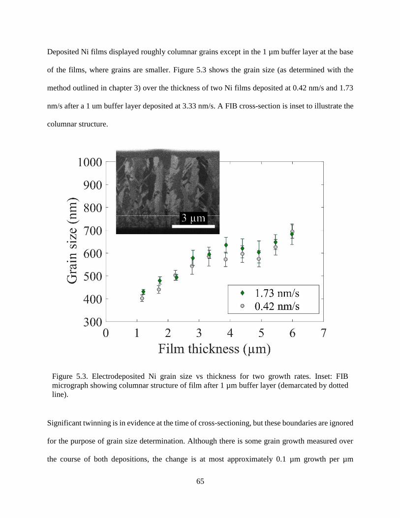
65
Deposited Ni films displayed roughly columnar grains except in the 1 µm buffer layer at the base
of the films, where grains are smaller. Figure 5.3 shows the grain size (as determined with the
method outlined in chapter 3) over the thickness of two Ni films deposited at 0.42 nm/s and 1.73
nm/s after a 1 um buffer layer deposited at 3.33 nm/s. A FIB cross-section is inset to illustrate the
columnar structure.
Significant twinning is in evidence at the time of cross-sectioning, but these boundaries are ignored
for the purpose of grain size determination. Although there is some grain growth measured over
the course of both depositions, the change is at most approximately 0.1 µm growth per µm
Figure 5.3. Electrodeposited Ni grain size vs thickness for two growth rates. Inset: FIB
micrograph showing columnar structure of film after 1 µm buffer layer (demarcated by dotted
line).

66
deposited, so it is reasonable to assume that the effects of the grain size change over short
thicknesses are minimal.
Steady-state stresses were determined from experiments structured as several depositions
performed in sequence at a number of different growth rates, after an initial 1 µm buffer layer. An
example experiment is summarized in figure 5.4. The buffer layer is necessitated by the lattice
mismatch between the Au conductive layer and Ni film, which is an additional source of stress
Figure 5.4. Electrodeposited Ni grain size vs thickness, growth rate vs thickness, and stress
thickness vs thickness for one experiment comprised of subsequent layers deposited at several
different growth rates in random order, each repeated once after an initial 1 µm buffer layer.

67
near the substrate. With the exception of the buffer layer, when the deposition of each layer begins
– after a pause of at least 120 seconds from the termination of the previous layer – the stress-
thickness quickly becomes linear, which indicates that a steady state has been achieved. There is
also no irreversible tensile stress buildup while deposition is paused, which supports the absence
of grain growth.
With the stress, growth rate, and grain size all known for each segment deposited, we can compare
the results to the kinetic model first introduced in chapter 2 with the form described in equation
5.1. For a uniform grain size, the steady state stress measured is in good agreement with the model;
with a grain size near 400 nm, the fit is shown in figure 5.5 for parameters in table 5.1.
Figure 5.5. Steady state stress of electrodeposited Ni fit to kinetic model described in text.

68
Because the stress in each layer is independent of previously deposited layers and grain growth is
extremely limited, for zone I films with known grain size and grain size evolution it is reasonable
to integrate the steady state model for stress thickness in equation 5.1 over the film thickness to
predict the stress evolution of a continuously deposited film. In this case, we can approximate the
continuously changing grain size 𝐿 as changing linearly with thickness such that
𝐿 = 𝐿1 + 𝛼 (ℎ𝑓 − ℎ1), (5.2)
where 𝐿1 is the grain size at height ℎ1 and 𝛼 is the rate that the grain size changes with film
thickness. If there is no grain size increase with film thickness, then alpha is zero and the grain
size is constant. For the two films deposited at 1.73 and 0.42 nm/s whose grain sizes are recorded
in figure 5.3, 𝛼 is approximately 0.05 nm/nm. This approximation can be used to fit the full stress
thickness evolution of the deposited films to the kinetic model. The results of this fitting are shown
in figure 5.6, and the parameters of the fit found are recorded in table 5.2.
The agreement between the model and the data is very good for both growth rates. The agreement
between the parameters found for continuous depositions and the parameters for paused deposition
L (μm) 𝝈𝑪,𝟎 (MPa) 𝝈𝑻 (MPa) 𝜷𝑫 (nm2/s)
0.4 -27.74 459.83 681.1
L (μm) 𝝈𝑪,𝟎 (MPa) 𝝈𝑻 (MPa) 𝜷𝑫 (nm2/s)
0.4 -147.8 336.5 431.7
Table 5.1. Kinetic model fitting parameters for steady-state paused electrodeposited Ni.
Table 5.2. Kinetic model fitting parameters for continuously electrodeposited Ni.
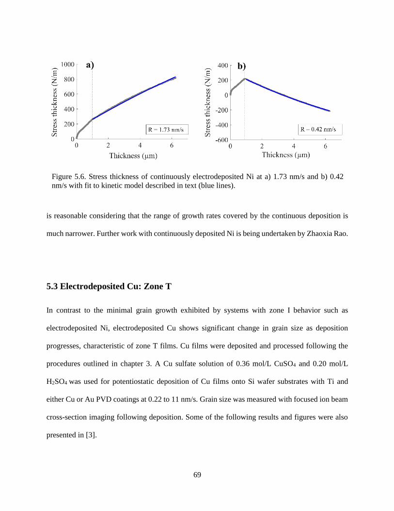
69
is reasonable considering that the range of growth rates covered by the continuous deposition is
much narrower. Further work with continuously deposited Ni is being undertaken by Zhaoxia Rao.
5.3 Electrodeposited Cu: Zone T
In contrast to the minimal grain growth exhibited by systems with zone I behavior such as
electrodeposited Ni, electrodeposited Cu shows significant change in grain size as deposition
progresses, characteristic of zone T films. Cu films were deposited and processed following the
procedures outlined in chapter 3. A Cu sulfate solution of 0.36 mol/L CuSO4 and 0.20 mol/L
H2SO4 was used for potentiostatic deposition of Cu films onto Si wafer substrates with Ti and
either Cu or Au PVD coatings at 0.22 to 11 nm/s. Grain size was measured with focused ion beam
cross-section imaging following deposition. Some of the following results and figures were also
presented in [3].
Figure 5.6. Stress thickness of continuously electrodeposited Ni at a) 1.73 nm/s and b) 0.42
nm/s with fit to kinetic model described in text (blue lines).
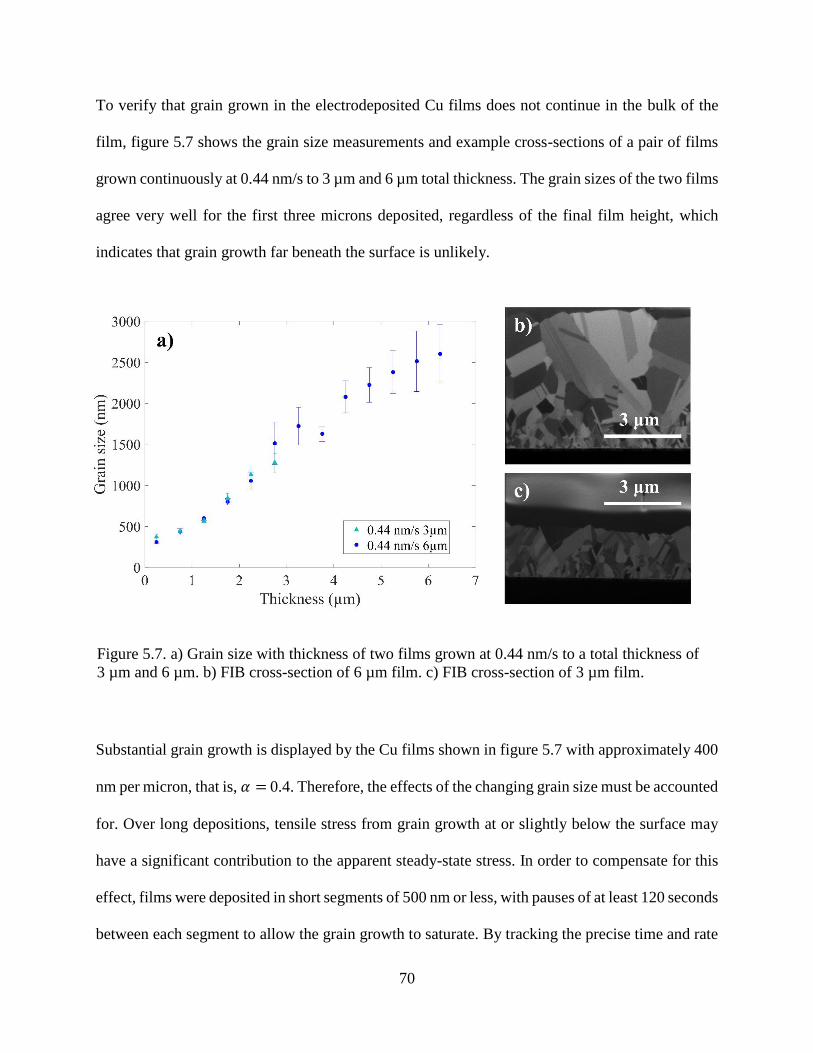
70
To verify that grain grown in the electrodeposited Cu films does not continue in the bulk of the
film, figure 5.7 shows the grain size measurements and example cross-sections of a pair of films
grown continuously at 0.44 nm/s to 3 µm and 6 µm total thickness. The grain sizes of the two films
agree very well for the first three microns deposited, regardless of the final film height, which
indicates that grain growth far beneath the surface is unlikely.
Substantial grain growth is displayed by the Cu films shown in figure 5.7 with approximately 400
nm per micron, that is, 𝛼 = 0.4. Therefore, the effects of the changing grain size must be accounted
for. Over long depositions, tensile stress from grain growth at or slightly below the surface may
have a significant contribution to the apparent steady-state stress. In order to compensate for this
effect, films were deposited in short segments of 500 nm or less, with pauses of at least 120 seconds
between each segment to allow the grain growth to saturate. By tracking the precise time and rate
Figure 5.7. a) Grain size with thickness of two films grown at 0.44 nm/s to a total thickness of
3 µm and 6 µm. b) FIB cross-section of 6 µm film. c) FIB cross-section of 3 µm film.

71
of each deposition period, grain size in the film measured following deposition could be correlated
to each segment of film growth, so that for each layer, the stress, growth rate, and grain size were
all known. Figure 5.8 a) shows an example plot of stress thickness during two depositions each
followed by pauses. The periods shown are at 0.44 nm/s and another at 0.92 nm/s. Figure 5.8 b)
shows a cross section of the complete film. The yellow highlighted growth period in a) corresponds
to the film section highlighted in yellow in b).
These short periods of film growth are associated with generally linear stress-thickness vs.
thickness, as expected for uniform films in the steady state. However, during the pauses, tensile
stress develops and reaches an equilibrium before the next deposition begins. This tensile stress is
not reversed when depositions begins again. These characteristics indicate that the source of this
Figure 5.8. (a) Electrodeposited Cu stress-thickness vs. thickness for periods of growth with
rates indicated in figure and stress-thickness vs. time for growth interrupts of approximately
120 s. Green lines are linear fits for constant slope expected during steady-state growth; red
lines are guides to illustrate stress relaxation during growth pauses. (b) FIB cross-section
micrograph of Cu film deposited including segments from (a). The yellow band is an indication
of where the growth interval in (a) correlates to film thickness in the micrograph.
(a)
(b)
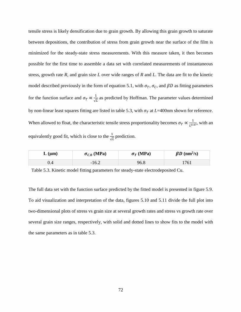
72
tensile stress is likely densification due to grain growth. By allowing this grain growth to saturate
between depositions, the contribution of stress from grain growth near the surface of the film is
minimized for the steady-state stress measurements. With this measure taken, it then becomes
possible for the first time to assemble a data set with correlated measurements of instantaneous
stress, growth rate R, and grain size L over wide ranges of R and L. The data are fit to the kinetic
model described previously in the form of equation 5.1, with 𝜎𝑇, 𝜎𝐶, and 𝛽𝐷 as fitting parameters
for the function surface and 𝜎𝑇 ∝1
√𝐿 as predicted by Hoffman. The parameter values determined
by non-linear least squares fitting are listed in table 5.3, with 𝜎𝑇 at L=400nm shown for reference.
When allowed to float, the characteristic tensile stress proportionality becomes 𝜎𝑇 ∝1
𝐿0.47, with an
equivalently good fit, which is close to the 1
√𝐿 prediction.
The full data set with the function surface predicted by the fitted model is presented in figure 5.9.
To aid visualization and interpretation of the data, figures 5.10 and 5.11 divide the full plot into
two-dimensional plots of stress vs grain size at several growth rates and stress vs growth rate over
several grain size ranges, respectively, with solid and dotted lines to show fits to the model with
the same parameters as in table 5.3.
L (μm) 𝝈𝑪,𝟎 (MPa) 𝝈𝑻 (MPa) 𝜷𝑫 (nm2/s)
0.4 -16.2 96.8 1761
Table 5.3. Kinetic model fitting parameters for steady-state electrodeposited Cu.

73
Overall, though there is some experimental error in the data, the predictions of the model agree
well with the experimental results, which provides support for the complex interrelations between
stress, growth rate, and grain size as captured by the model presented and the underlying physical
mechanisms proposed. The competition between tensile stress arising from individual layer
coalescence and compressive stress from adatom insertion provides a balance which can be used
to describe many trends observed in figures 5.9-5.11.
The Hoffman mechanism alone, which assumes a tensile stress from grain boundary formation
proportional to 1
√𝐿, predicts that smaller grain size should always be associated with more tensile
Figure 5.9. Electrodeposited Cu steady-state stress vs growth rate and grain size. Stress was
calculated from stress-thickness vs thickness measurements. The function surface shows the
kinetic model described in the text with parameter values determined from fitting the data.

74
stress. In the data, the same range of grain sizes show very different trends depending on the growth
rate, and none of them align with the Hoffman mechanism predictions. At low or high growth
rates, the change in the stress with grain size is less than would be expected over the experimental
Figure 5.10. a-f) Electrodeposited Cu steady-state stress vs grain size at a growth rate indicated
on figure. Solid lines are a fit to model with parameters in table 5.3.

75
range; at 1.8 nm/s in particular, figure 5.10 c), there is a clear transition from tensile stress at higher
grain size to compressive stress at low grain size. The combination of compressive and tensile
mechanisms is necessary to describe the data. However, even at the highest growth rate, where the
stresses are most tensile, the Hoffman mechanism is insufficient. In equation 5.1, there is another
contribution of the grain size: in the exponential term, where it mitigates the tensile stress from
layer coalescence with the effect of adatom insertion, and reduces the stress dependence on grain
size at high growth rates. Though the agreement between the model and the data is not perfect and
there is large experimental error, the predictions of the model are consistent with the experimental
Figure 5.11. a-d) Electrodeposited Cu steady-state stress vs growth rate at ranges of grain size
indicated on figure. Points are data averaged for each growth rate with measured grain size
within the given range. Solid and dashed lines are a fit to model with parameters in table 5.3.

76
observations. The highly varied relations between the stress and grain size with different growth
rates illustrates why both variables must be considered in future experiments.
In figure 5.11, there is clear agreement between stress predicted by the model over a wide range
of growth rates for a narrow range of grain sizes and the average steady-state stress measured for
each growth rate at those grain sizes. Again we see that at smaller grain sizes, the predicted change
in stress varies more dramatically with small changes at intermediate growth rates, and not at very
low or high growth rates. As the grain sizes increases, the same change in grain size is predicted
to have less effect on the film stress.
The next chapter will discuss zone II microstructural evolution, where substantial tensile stress is
contributed by grain growth in the bulk of the film and additional factors of high atomic mobility
must be considered as well.
References
[1] J. A. Thornton, Journal of Vacuum Science and Technology 12 (4), 830-835 (1975).
[2] A. Engwall, Z. Rao and E. Chason, Materials & Design 110, 616-623 (2016).
[3] A. Engwall, Z. Rao and E. Chason, Journal of The Electrochemical Society 164 (13),
D828-D834 (2017).

77
Chapter 6
Stress Evolution Models for Zone II Microstructure
In the zone model of microstructure evolution introduced in section 5.1, in order of increasing
atomic mobility, zone I films undergo little or no grain growth during deposition, zone T films
experience grain growth at or near the surface of the film, and zone II films are characterized by
grain growth both at the surface and through the bulk of the film. Unlike zone I and zone T films
discussed in the previous chapter, zone II films are deposited under conditions of high atomic
mobility, and their structure is typified by columnar grains which increase in diameter as the film
is grown. This grain growth beneath the surface introduces a complicating factor in analyzing the
stress produced by these films. The kinetic model for stress generation introduced in chapter 2 is
formulated to describe a system with stress generated at the surface of the film, but grain growth
in the bulk of the film necessitates an extension of this model to consider additional effects. This
chapter will present two options for analyzing zone II films. The first, or “low mobility” model,
supplements the model of stress generated at the triple junction as used in previous chapters with
stress generated by grain growth in the bulk. The second, “high mobility” model, differs
significantly in formulation as it allows for atomic diffusion in the grain boundaries as would be
expected in a high mobility system. Both of these models will be used to analyze a series of
experiments published by Carl Thompson and Hang Yu [1] where high-purity Ni films were
deposited with e-beam evaporation at temperatures ranging from 300-473 K at 0.05 nm/s and
growth rates ranging from 0.03 to 0.25 nm/s at 300 K. The films displayed behavior consistent
with zone II categorization: the grain size of the films increased linearly with film thickness and
the films maintained a columnar structure.

78
6.1 Grain growth in zone II films
First, it is necessary to discuss the stress generated by grain growth in the bulk of the film, i.e., not
at the surface. Grain boundaries are areas of high disorder compared to the crystalline lattice of a
grain interior. Therefore, the volume of a grain boundary contains fewer atoms than the same
volume of ordered lattice. Because the process of grain growth involves the reduction of the total
number of grain boundaries, the density of the final film is higher. In the absence of external forces,
the film would contract. Thin films anchored to an inflexible substrate instead see an increase in
tensile stress. The stress generated by grain growth in one independent layer i, can be described as
𝜎𝑖,𝑔𝑔 = 𝑀𝑓∆𝑎 (1
𝐿0−
1
𝐿), (6.1)
where 𝑀𝑓 is the biaxial modulus of the film, ∆𝑎 is the excess volume annihilated as a unit of grain
boundary is transformed into ordered crystal (approximately one lattice spacing), 𝐿0 is the initial
grain size, and 𝐿 is the final grain size [2].
When considering the stress in more than one layer, it becomes important to account for the fact
that the grain size in a zone II film increases with film thickness. The rate of increase is defined
here as α, which is approximated as a linear term. This approximation is supported by experimental
grain size measurements of the final Ni films [1]. With a linear α, the grain size of the film when
it is grown to thickness ℎ is 𝐿0 + αℎ, where 𝐿0 is now the initial grain size of the bottom layer.
The cumulative stress thickness due to grain growth in each layer for a film of final thickness ℎ𝑓
is then:
𝜎𝑔𝑔ℎ𝑓 = 𝑀𝑓∆𝑎 ∫ (1
𝐿0 + αℎ−
1
𝐿0 + αℎ𝑓)
ℎ𝑓
0
𝑑ℎ. (6.2)

79
Performing the integration yields an expression for the stress-thickness of a film of total thickness
ℎ𝑓:
𝜎𝑔𝑔ℎ𝑓 = 𝑀𝑓∆𝑎 (1
𝑎ln (
𝐿0 + αℎ𝑓
𝐿0) −
ℎ𝑓
𝐿0 + αℎ𝑓). (6.3)
The change in stress thickness due to grain growth as new layers are deposited is then
𝑑𝜎𝑔𝑔ℎ𝑓
𝑑ℎ𝑓= 𝑀𝑓∆𝑎
αℎ𝑓
(𝐿0 + αℎ𝑓)2 . (6.4)
This expression can be used to determine the tensile stress generated by grain growth in a thin film
as the film height increases. As in [1] following [3], typical parameter values are taken as 𝑀𝑓=290
GPa for Ni and ∆𝑎 = 0.1 nm.
6.2 Low mobility model
In a zone II system with low atomic mobility in the grain boundaries, there are three primary
sources of stress to consider. In addition to the tensile stress from grain growth which occurs
throughout the film as discussed above, the two previously introduced mechanisms of stress
generation are still active at the surface of the film. Each new layer snaps together at the top of the
grain boundary to generate tensile stress, and atom insertion into the topmost layer of the newly
formed grain boundary generates compressive stress. These two stresses generated at the film
surface are locked into each layer once another layer has formed a new top section of grain
boundary, but stress from grain growth will continue to increase in previously deposited layers as
the film becomes thicker. Thus, we have stress from the grain boundary triple junctions, 𝜎𝑔𝑏, such
that

80
𝑑𝜎𝑔𝑏ℎ𝑓
𝑑ℎ𝑓= 𝜎𝐶 + (𝜎𝑇 − 𝜎𝐶) ∙ 𝑒
(−𝛽𝐷𝐿
∙ 1
𝜕ℎ𝑔𝑏
𝜕𝑡
)
. (6.5)
where 𝜎𝐶 is the compressive stress parameter, the tensile stress parameter 𝜎𝑇 ∝1
√𝐿 following the
Hoffman prediction discussed previously, 𝛽 is the kinetic parameter defined in equation 2.8 as
𝛽 =4𝐶𝑠𝑀𝑓Ω
𝑘𝑇, D is effective diffusivity with the form 𝐷0𝑒−
𝐸𝑎𝑘𝑇⁄
, and grain boundary velocity 𝜕ℎ𝑔𝑏
𝜕𝑡
can be approximated after a film has coalesced as the average growth rate of the film, 𝑅.
The thickness derivative of stress thickness from grain growth is defined in equation 6.4.
Combining these elements, the total stress in each layer can be described as
𝑑𝜎ℎ𝑓
𝑑ℎ𝑓= 𝜎𝐶 + (𝜎𝑇 − 𝜎𝐶) ∙ 𝑒(−𝛽
𝐷𝐿
1𝑅
) + 𝑀𝑓∆𝑎αℎ𝑓
𝐿2, (6.6)
where 𝐿 = 𝐿0 + αℎ𝑓, changing with each layer added to the film. To allow direct comparison with
experimental data, equation 6.6 is integrated over the thickness of the film. For this expression,
the parameters necessary to fit the model to a data set are 𝜎𝐶, 𝜎0, 𝐿0, α, 𝛽𝐷, 𝑅, and 𝑀𝑓∆𝑎. As
previously introduced in section 4.4 for the discussion of evaporated Ag, the kinetic parameters
𝛽𝐷 as a function of temperature have the form
𝛽𝐷 =(𝛽𝐷)0𝑒−
𝐸𝑎𝑘𝑇⁄
𝑘𝑇, (6.7)
which means that rather than treating 𝛽𝐷 as one parameter, it is possible to instead fit one constant,
(𝛽𝐷)0, and the activation energy 𝐸𝑎.
81
Unlike the evaporated Ag experiments, for which very little grain size data was available, Yu and
Thompson’s confidence in the linear evolution of the grain size and zone II microstructure for
evaporated Ni presents an opportunity for consideration of the combined effects of growth rate,
grain size, and temperature. High purity Ni films were deposited by e-beam evaporation under
ultra high vacuum conditions. Substrates were 50 x 18 x 0.2 mm cantilevers cut from (1 0 0) Si
wafers and coated with 33 nm silicon nitride [1]. Grain size was measured with image analysis of
plan-view bright-field tunneling electron microscope (TEM) images of films grown at 300, 373,
and 473 K, and grain size increased linearly with thickness at all temperatures at a rate of
approximately 0.298 nm per nm. TEM imaging of ion-milled cross-sections of deposited films
confirmed that grains were columnar after deposition, which is evidence for the films being zone
II. Films were deposited at 373 K and 0.03, 0.05, 0.08, 0.13, and 0.25 nm/s, as well as 0.05 nm/s
and 300, 333, 373, 398, 423, and 473 K. Note that there are two unique data sets grown at 0.05
nm/s and 373 K. The films grown at 0.05 nm/s but variable temperature were deposited
continuously, while the films deposited at varying rates were all grown to 15 nm at 0.05 nm/s
before growth continued at the indicated rate [1].
6.2.1 Model fitting
The data obtained from these experiments were fit to the model described above in the form of
equation 6.6. Parameter values were determined by non-linear least squares fitting, with one
additional parameter permitting an offset between the data and the initial point of the fitted model.
Fitting was begun from 15 nm thickness, well past the point of coalescence, because of the
discontinuity in growth for the films which continued at different growth rates. Grain size and
grain growth parameter constraints were enforced based on the experimental measurements: the

82
grain size at 15 nm was constrained to a range of 5-15 nm, and the rate of grain size increase α
was limited to 0.298 ± 20%. For other parameters, κ offset was limited to 1 N/m, (𝛽𝐷)0 was permitted
to vary 5% for each data set, and a singular value of Mf∆a for all data sets was limited to within
10% of 29 GPa. Single values for all data sets were also found for the 𝛽𝐷 activation energy Ea and
tensile parameter σT. For σC, unique values were permitted for each deposition. The results of this
fitting are presented in figure 6.1 for data at varying rates deposited at 373K, figure 6.2 for variable
temperature data deposited at 0.5 nm/s, and table 6.1 for parameter values.
Figure 6.1. Stress thickness of evaporated Ni deposited at 373 K and a range of growth rates
as indicated on plot. Black lines are fit to low mobility model for zone II microstructure
described in text.

83
The model predictions are in very good agreement with the experimental findings despite the
parameter constraints. The different stress evolutions can be described well across variations in
both growth rate and temperature, with primarily tensile, primarily compressive, and intermediate
behaviors included, using one self-consistent set of parameters and grain growth conditions
consistent with experimental observations.
With a unique value of the compressive stress parameter 𝜎𝐶 allowed for each data set, some
interesting trends appear. 𝜎𝐶 was found to be strongly linear with growth rate at 373 K, with an
Figure 6.2. Stress thickness of evaporated Ni deposited at 0.05 nm/s and a range of temperatures
as indicated on plot. Black lines are fit to low mobility model for zone II microstructure
described in text.

84
Arrhenius dependence on temperature for films deposited at 0.05 nm/s. Plots of these trends are
shown in figure 6.3. The activation energy found for 𝜎𝐶 with the linear fit in figure 6.3 (b) is 0.0725
eV, while the fitted linear relation between 𝜎𝐶 and 𝑅 in 6.3 (a) is 𝜎𝐶 = -15.083𝑅-0.61.
Reconciling these two clear trends in one comprehensive form for 𝜎𝐶 as a function of growth rate
and temperature, 𝜎𝐶 becomes
R
(nm/s)
T(K) L at
15 nm
(nm)
𝝈𝑪
(GPa)
𝝈𝑻 at
L=400
nm
(GPa)
𝑬𝒂
(eV)
𝜷𝑫
(nm2/s)
𝑴𝒇∆𝒂
(GPa)
𝛂 𝜿 offset
at 15 nm
(N/m)
0.05 300 8.584 -2.363 0.393 0.117 1.118 26.100 0.358 0.128
0.05 333 8.517 -1.727 - - 1.597 - 0.276 -0.069
0.05 373 10.897 -1.409 - - 2.069 - 0.358 0.132
0.05 398 11.429 -1.267 - - 2.437 - 0.358 0.137
0.05 423 13.161 -1.110 - - 2.805 - 0.358 0.461
0.05 473 15.000 -0.786 - - 3.892 - 0.238 0.371
0.03 373 15.000 -0.938 - - 2.069 - 0.358 0.453
0.05 373 11.740 -1.380 - - 2.069 - 0.358 0.419
0.08 373 7.887 -2.182 - - 2.069 - 0.302 -0.068
0.13 373 15.000 -2.184 - - 2.287 - 0.238 1.000
0.25 373 14.163 -4.469 - - 2.069 - 0.238 1.000
Table 6.1. Low mobility kinetic model fitting parameters for zone II evaporated Ni.

85
𝜎𝐶 = 𝐴0 +𝐴1𝑅
𝑒−𝐸𝑎
𝐶
𝑘𝑇⁄
, (6.8)
which contains a dependence on the ratio R/D. 𝐴0 and 𝐴1 are constants, and 𝐸𝑎𝐶 is an activation
energy. Fitting this equation to the values of 𝜎𝐶 in table 6.1 yields parameter values of 𝐴0 = -0.387,
𝐴1 = -0.786, and 𝐸𝑎𝐶 = 0.102 with similarly good agreement as the individual linear fits show
above.
Although there is very good agreement between the experimental data and the overall fitted model
for low-mobility zone II films, there are some points of concern. The values found for the
activation energy for 𝛽𝐷 are lower than previously reported values for Ni surface diffusion, which
are closer to 0.2 eV [1, 4]. Additionally, the magnitude of 𝜎𝐶 becomes unreasonably large at low
temperature and high growth rates. However, the primary concern with the low mobility model is
that it does not allow for any atomic diffusion in the grain boundaries. A system with zone II grain
(a) (b)
Figure 6.3. (a) Low mobility kinetic model fitted parameter 𝜎𝐶 vs growth rate R for evaporated
Ni deposited at 373 K. (b) Arrhenius plot of ln(−𝜎𝐶) vs 1/kT for Ni deposited at 0.05 nm/s.
Solid lines are linear fits.

86
growth is characterized by high atomic mobility, which is necessary for grain boundary motion in
the bulk of the film. As atomic diffusion along a grain boundary is easier than grain boundary
diffusion through a lattice, such a system should have high atomic mobility through the grain
boundaries. Without atoms moving through the grain boundaries, layers toward the bottom of the
film which had the smallest grain size when first deposited experience more grain growth and
therefore generate more tensile stress than layers above, leading to a sharp gradient in film stress.
If atoms can penetrate the film through the grain boundaries, this stress is ameliorated by atoms
from the top of the grain boundaries diffusing to the base of the film instead of accumulating in
only the most accessible, topmost layer. Since there is less buildup of compressive stress in the
topmost layer, it is easier for additional atoms to jump from the surface into the grain boundary.
In a zone II film, there should be no stress gradient in the film, and the uniform stress in the bulk
should inform the kinetics of atoms interacting with the grain boundaries at the surface. The next
section introduces a new form of the model which takes these considerations into account.
6.3 High mobility model
A system with high atomic mobility in the grain boundaries presents unique challenges for
modeling the stress evolution. If at any point in the deposition a stress gradient develops in the
film, atoms can diffuse through the grain boundaries from a layer with more compressive stress to
a layer with more tensile stress. If the time scale on which this diffusion occurs is small compared
to the deposition rate, then the stress is effectively uniform in the film. Whether that stress is tensile
or compressive can and does change as deposition progresses, due to factors such as grain growth
at the surface and grain growth in the bulk of the film. The mechanisms by which stresses develop
at the surface of the film in the grain boundary triple junctions in a high mobility system are the

87
same as in a low mobility system, that is, tensile stress arises from layers snapping together and
compressive stress is generated from adatom insertion. Stress in the bulk of the film from grain
growth develops as described in section 6.1, with tensile stress generated through the thickness of
the film as grain boundaries are annihilated. However, a system with high atomic mobility in the
grain boundaries cannot consider stress generation as only occurring in isolated layers that do not
affect each other. Atoms that jump from the surface into the grain boundary may either stay and
incorporate into the topmost layer of the film or diffuse down the grain boundary to interior layers.
When the bulk of the film is more tensile than the topmost layer, atoms are driven to travel down
the grain boundaries to more tensile layers to alleviate some of the stress. Conversely, if the bulk
of the film is more compressive than the topmost layer, there will be a positive pressure of atoms
traveling toward the surface to relieve some of the compressive stress, which means a reduced
driving force for atoms jumping from the surface. Unlike in low mobility systems discussed
previously, a kinetic model for high mobility stress evolution must consider the relationship
between the developing stress at the top of the grain boundaries and the stress in the bulk.
Therefore, the stress must be analyzed with respect to the whole film rather than as an integral of
isolated layers.
Adapting equation 1.1 which relates wafer curvature to the average stress in a film and equation
1.2 which defines the average stress in terms of an integral over the film thickness allows the
definition of a normalized curvature �� equivalent to the stress thickness of the film,
�� =𝜅𝑀𝑠ℎ𝑠
2
6= ∫ 𝜎(𝑧)𝑑𝑧 = ⟨𝜎⟩ℎ𝑓 .
ℎ𝑓
0
(6.9)

88
𝑀𝑠 is the biaxial modulus of the substrate, ℎ𝑠 is the substrate thickness, and ⟨𝜎⟩ is the average
stress, which is uniform through the thickness of the film for systems with high atomic mobility.
Insertion of any number of atoms 𝑁 into the grain boundary induces strain 휀 in the film such that
휀 = −𝑁𝑎2
𝐿ℎ, (6.10)
a negative quantity because the strain is compressive. Applying Hooke’s law,
𝜎 = 𝑀𝑓휀, (6.11)
curvature due to this strain is then
�� = 𝜎ℎ𝑓 = −𝑀𝑓𝑁𝑎2
𝐿. (6.12)
The rate of change of the curvature depends on the rate of insertion of the atoms
𝑑��
𝑑𝑡=
𝑑𝜎ℎ𝑓
𝑑𝑡= −
𝑀𝑓𝑎2
𝐿
𝑑𝑁
𝑑𝑡. (6.13)
As in equation 2.4,
𝜕𝑁
𝜕𝑡= 4𝐶𝑠
𝐷Δ𝜇
𝑎2𝑘𝑇, (6.14)
but the chemical potential difference Δ𝜇 depends on the stress in the layer, which in a high mobility
system is not independent; the stress in the layer is the average stress in the film. So, equation 2.3
is modified to
Δ𝜇 = 𝜇𝑠 − 𝜇𝑔𝑏 = 𝛿𝜇𝑠 + ⟨𝜎⟩Ω = Ω(⟨𝜎⟩ − 𝜎𝐶) (6.15)
Combining equations 6.13, 6.14, and 5.15 and substituting in 𝛽 gives

89
𝑑��
𝑑𝑡=
𝑑𝜎ℎ𝑓
𝑑𝑡= −
𝛽𝐷
𝐿(⟨𝜎⟩ − 𝜎𝐶). (6.16)
Since ⟨𝜎⟩ =��
ℎ𝑓, the rate of change of curvature from atom insertion with thickness is then
𝑑��
𝑑ℎ𝑓= −
𝛽𝐷
𝑅𝐿(
��
ℎ𝑓− 𝜎𝐶). (6.17)
The stress generated by the coalescence of the top layer of atoms to form new segments of grain
boundary is the same in a high mobility system as in a low mobility system, 𝜎𝑇 ∝1
√𝐿. In terms of
changing curvature with thickness, that is
𝑑��
𝑑ℎ𝑓= 𝜎𝑇 . (6.18)
From equations 6.4 and 6.9, the expression for curvature change with thickness due to grain growth
can be written as
𝑑��
𝑑ℎ𝑓=
𝑑𝜎𝑔𝑔ℎ𝑓
𝑑ℎ𝑓= 𝑀𝑓∆𝑎
αℎ𝑓
(𝐿0 + αℎ𝑓)2 (6.19)
Combining the effects of atom insertion, grain boundary formation, and grain growth as presented
in equations 6.17, 6.18, and 6.19 yields the expression
𝑑��
𝑑ℎ𝑓= −
𝛽𝐷
𝑅𝐿(
��
ℎ𝑓− 𝜎𝐶) + 𝜎𝑇 + 𝑀𝑓∆𝑎
αℎ𝑓
(𝐿0 + αℎ𝑓)2 , (6.20)
which can be integrated for a predicted curvature evolution to compare directly to experimental
data.

90
6.3.1 Model fitting
Fitting to the data was begun at h=15 nm, as with the low mobility model, in order to avoid the
regimes of film nucleation and coalescence as well as the discontinuity in growth at 15 nm
thickness for the films not grown at 0.05 nm/s after that point. Since the stress in each new layer
depends on the existing curvature ��, the effective initial value at 15 nm is an important fitting
parameter, ��0. Fitted values for ��0 were found to be much less tensile than the data would suggest.
It may be that the microstructure of the initial layers of the film or strong adhesion to the substrate
prevents atom diffusion to the lowest layers of the film even when mobility in the grain boundaries
is otherwise high. Therefore, the stress contributions of the initial layers of the film were
discounted, and it was assumed that this exclusion layer did not significantly interact with the rest
of the film while deposition continued. The height of this exclusion layer, ℎ𝑒𝑥, was consistently
found to be approximately 13 nm. The result of fitting this model to data from the evaporated Ni
experiments previously described are presented in figures 6.4 and 6.5, with fitted parameter values
recorded in table 6.2.
The model predictions are in very good agreement with the experimental data with imposed
parameter constraints similar to those used for fitting the low mobility model above. The grain size
at 15 nm was limited to 5-15 nm, and the rate of grain size increase α was limited to 0.298 ± 20%.
(𝛽𝐷)0 was permitted to vary 5% for each data set from a strict Arrhenius relation, while Mf∆a was
set to within 10% of 29 GPa, constant for all data sets. Single values for all data sets were also
found for the activation energy Ea and tensile parameter σT. For σC, the fit shown allows a unique
value for each data set. The additional parameter ��0 for the initial curvature at h=15 was

91
constrained to within 1 N/m of the difference between the measured curvature at the start of fitting
and at the height of the exclusion layer, ��(15) − ��(ℎ𝑒𝑥).
The same trends observed in the low mobility zone II model for the fitted values of the compressive
stress parameter 𝜎𝐶 are also in evidence in the high mobility model. 𝜎𝐶 increases in magnitude
linearly with growth rate and decreases with temperature. A plot of 𝜎𝐶 against growth rate for films
grown at 373 K and an Arrhenius plot of ln(−𝜎𝐶) vs. 1/kT for films grown at 0.05 nm/s are shown
with linear fits in figure 6.6. The activation energy for 𝜎𝐶 was found to be 0.039 eV, while the
linear equation to describe the relation between 𝜎𝐶 and 𝑅 is 𝜎𝐶 = -5.29𝑅-0.22.
Figure 6.4. Stress thickness of evaporated Ni deposited at 373 K and a range of growth rates as
indicated on plot. Black lines are fit to high mobility model for zone II microstructure described
in the text.

92
Equation 6.8 above may again be used to encompass both trends of 𝜎𝐶 with growth rate and
temperature. Fitting the results in table 6.2 with equation 6.8 to comprehensively describe how 𝜎𝐶
changes with experimental conditions generates the parameter values of 𝐴0 = -0.212, 𝐴1 = -0.3835,
and 𝐸𝑎𝐶 = 0.084 for an equally good agreement with the observed values of 𝜎𝐶 as the separate fits
shown in figure 6.6.
Figure 6.5. Stress thickness of evaporated Ni deposited at 0.05 nm/s and a range of
temperatures as indicated on plot. Black lines are fit to high mobility model for zone II
microstructure described in text.
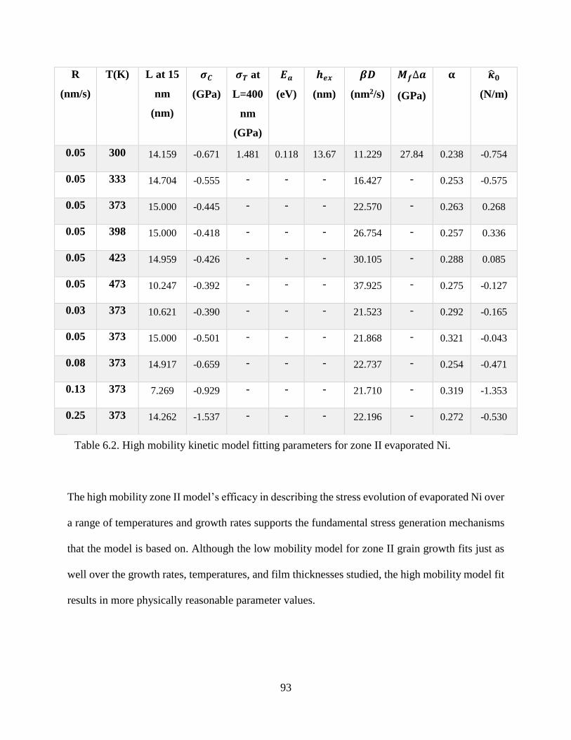
93
R
(nm/s)
T(K) L at 15
nm
(nm)
𝝈𝑪
(GPa)
𝝈𝑻 at
L=400
nm
(GPa)
𝑬𝒂
(eV)
𝒉𝒆𝒙
(nm)
𝜷𝑫
(nm2/s)
𝑴𝒇∆𝒂
(GPa)
𝛂 ��𝟎
(N/m)
0.05 300 14.159 -0.671 1.481 0.118 13.67 11.229 27.84 0.238 -0.754
0.05 333 14.704 -0.555 - - - 16.427 - 0.253 -0.575
0.05 373 15.000 -0.445 - - - 22.570 - 0.263 0.268
0.05 398 15.000 -0.418 - - - 26.754 - 0.257 0.336
0.05 423 14.959 -0.426 - - - 30.105 - 0.288 0.085
0.05 473 10.247 -0.392 - - - 37.925 - 0.275 -0.127
0.03 373 10.621 -0.390 - - - 21.523 - 0.292 -0.165
0.05 373 15.000 -0.501 - - - 21.868 - 0.321 -0.043
0.08 373 14.917 -0.659 - - - 22.737 - 0.254 -0.471
0.13 373 7.269 -0.929 - - - 21.710 - 0.319 -1.353
0.25 373 14.262 -1.537 - - - 22.196 - 0.272 -0.530
The high mobility zone II model’s efficacy in describing the stress evolution of evaporated Ni over
a range of temperatures and growth rates supports the fundamental stress generation mechanisms
that the model is based on. Although the low mobility model for zone II grain growth fits just as
well over the growth rates, temperatures, and film thicknesses studied, the high mobility model fit
results in more physically reasonable parameter values.
Table 6.2. High mobility kinetic model fitting parameters for zone II evaporated Ni.
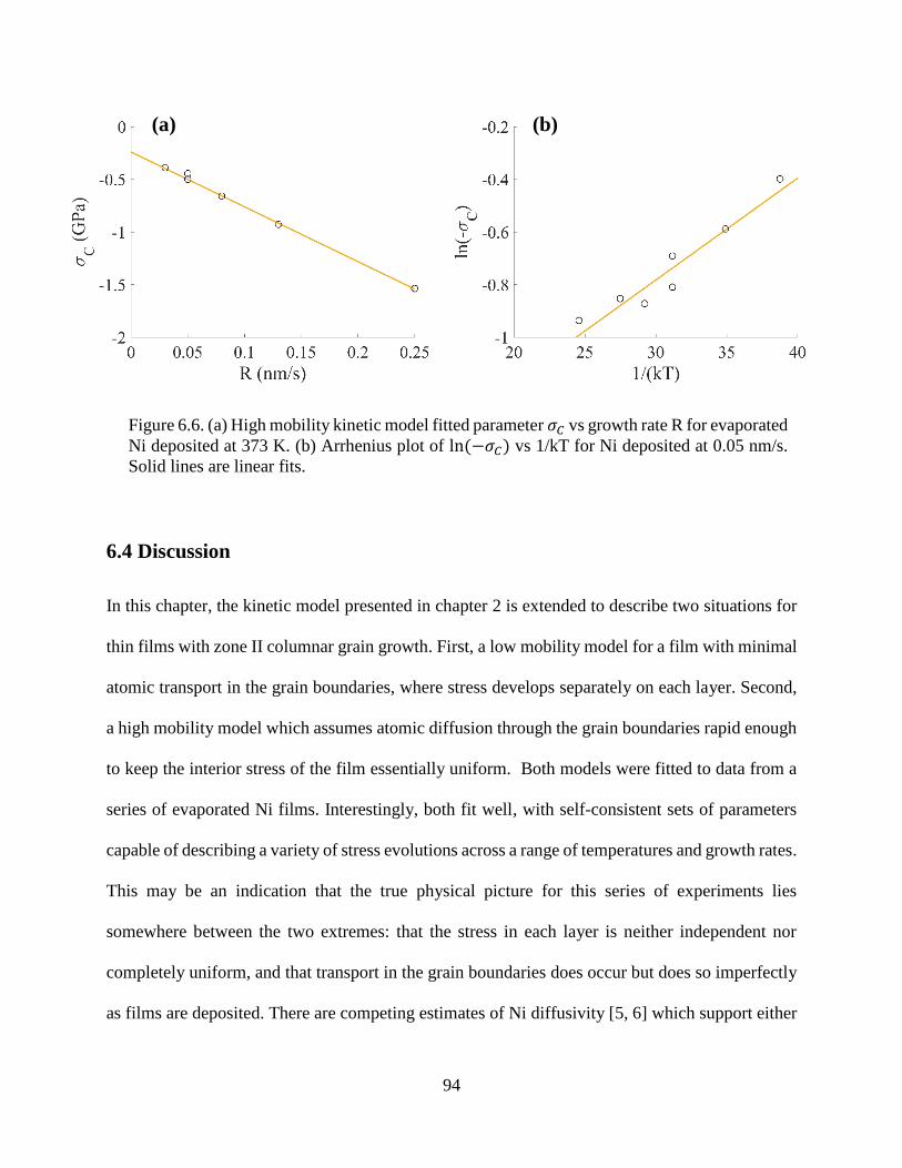
94
6.4 Discussion
In this chapter, the kinetic model presented in chapter 2 is extended to describe two situations for
thin films with zone II columnar grain growth. First, a low mobility model for a film with minimal
atomic transport in the grain boundaries, where stress develops separately on each layer. Second,
a high mobility model which assumes atomic diffusion through the grain boundaries rapid enough
to keep the interior stress of the film essentially uniform. Both models were fitted to data from a
series of evaporated Ni films. Interestingly, both fit well, with self-consistent sets of parameters
capable of describing a variety of stress evolutions across a range of temperatures and growth rates.
This may be an indication that the true physical picture for this series of experiments lies
somewhere between the two extremes: that the stress in each layer is neither independent nor
completely uniform, and that transport in the grain boundaries does occur but does so imperfectly
as films are deposited. There are competing estimates of Ni diffusivity [5, 6] which support either
(a) (b)
Figure 6.6. (a) High mobility kinetic model fitted parameter 𝜎𝐶 vs growth rate R for evaporated
Ni deposited at 373 K. (b) Arrhenius plot of ln(−𝜎𝐶) vs 1/kT for Ni deposited at 0.05 nm/s.
Solid lines are linear fits.

95
high mobility or low mobility behavior. In either case, the stress contribution of grain growth under
the surface is a key component to the total stress evolution, insufficient by itself to explain the
range of complex evolutions observed but important in conjunction with other tensile and
compressive stresses generated where grain boundaries meet the surface. The grain size and rate
of grain size increase with thickness 𝛼 for all films was not permitted to vary more than 20% from
the experimentally measured value, so the Chaudhari stress for each film is similar. Therefore,
nearly all the variation in stress evolution is due to stress generated at the triple junctions. Figure
6.7 shows an example of the separate and combined component contributions with ℎ𝜎𝑔𝑔 and ℎ𝜎𝑔𝑏
calculated by the model for the film deposited at 0.25 nm/s and 373 K. The change in curvature as
the film grows is primarily dependent on the shape of ℎ𝜎𝑔𝑏, which depends on growth rate and
temperature.
For both the low mobility and the high mobility model models, σC was found to be strongly linear
with growth rate with an exponential dependence on 1/T. Both trends were successfully captured
with comprehensive equation 6.8 describing σC as a function of growth rate and temperature with
three fitted parameters: a constant 𝐴0, prefactor 𝐴1, and an activation energy 𝐸𝑎𝐶 , which supports
a σC dependence on the ratio 𝑅/𝐷. In equation 2.7, σC is defined as being proportional to chemical
potential change on the film surface. A proportionality between σC and growth rate indicates an
increase in the driving force for atom insertion into the grain boundary which is consistent with
increased supersaturation on the surface with higher deposition rates. Conversely, increasing
temperatures increase diffusivity and atom mobility, which lowers surface supersaturation by
enabling adatom diffusion to sinks like defects and grain boundaries. Therefore, the 𝑅/𝐷
dependence observed is supported by the fundamental mechanisms of the kinetic model regardless

96
of whether there is high or low mobility in the grain boundaries. However, the non-zero constant
𝐴0 implies that even when no growth is occurring, σC has a value. Supersaturation of atoms on the
surface is unlikely without deposition flux, so there may be another mechanism in play.
These trends in σC with temperature and growth rate were not observed in electrodeposited films
or evaporated Ag. In previous chapters, σC was a model parameter always held constant across
growth rate or temperature because there was no evidence to support doing otherwise. For this set
of experiments, changing σC proved to be necessary to arrive at good fits. Although it seems likely
from the evidence here that σC can change with deposition conditions, this is the first set of data
Figure 6.7. Stress thickness of evaporated Ni deposited at 0.25 nm/s and 373K. Dotted purple
line and dashed blue line are fit to components of high mobility model for zone II microstructure
described in text; solid black line represents the combined model.

97
which captures the stress evolution for a material with several growth rates, several temperatures,
and microstructure evolution known well enough to isolate the stress from grain growth and predict
the surface grain size contribution to the parameter ratio -𝛽𝐷/𝑅𝐿. All of these factors are necessary
in order to capture and accurately describe film stress in a regime where σC changes significantly
enough to be measured.
A constant value of σC may still be a reasonable approximation for the experiments investigated
in previous chapters. The growth rates for electrodeposition experiments were orders of magnitude
higher than for evaporation. The rate of atom incorporation in rapidly deposited systems may be
outpaced by the rate of deposition such that atoms have insufficient time to jump into the grain
boundary before the height of the grain boundary increases. The linearity of σC with growth rate
would then not be sustained at high growth rates. If equation 6.8 does hold true at high growth
rates, it may be that the effects were too subtle to capture in electrodeposition experiments, either
because the range of growth rates was too narrow or due to differences in electrodeposited vs
evaporated film growth. Increased roughness and more abundant defects on an electrodeposited
surface provide more sinks for mobile atoms compared to evaporated films, which could affect the
mechanisms for atom diffusion and incorporation. Further research into the relationship between
growth rate and surface chemical potential is necessary, especially in different growth regimes.
Another parameter with surprising fitted results is the activation energy for 𝛽𝐷, which the high
and low mobility models both find to be approximately 0.12 eV. These values for the activation
energy of the jump from the film surface into the grain boundary are somewhat lower than either
0.22 eV for surface diffusion [4] or 0.45 eV for diffusion through a grain boundary [7]. However,
Leib and Thompson found an activation energy for reversible stress relaxation in Au films which,

98
although most likely due to atom diffusion out of the grain boundary and onto the surface, was
also much lower than those expected for lattice diffusion, surface diffusion, or gain boundary
diffusion [8]. This is an indication that atom behavior around triple junctions is not well
understood. It may be that the actual atomic jump relevant is not quite analogous to either surface
diffusion or grain boundary diffusion, or that an abundance of defects in the particularly small
grains effectively assists atomic diffusion. Further investigation is needed, with deposition
experiments that cover a range of temperatures and carefully monitor grain size as well as stress
and modeling experiments to study the atomic transition between the film surface and grain
boundary. In particular, terrace size may be an important factor in determining how easily atoms
may jump from the surface into the grain boundary; narrow atomic ledges around grain boundaries
require adatoms outside the immediate vicinity of the grain boundary to attach and detach from
step edges while diffusing.
References
[1] H. Z. Yu and C. V. Thompson, Acta Materialia 67, 189-198 (2014).
[2] P. Chaudhari, Journal of Vacuum Science and Technology 9 (1), 520-522 (1972).
[3] M. Meyers and K. Chawla, (Cambridge University Press).
[4] T.-Y. Fu and T. T. Tsong, Surface science 454, 571-574 (2000).
[5] H. Z. Yu, J. S. Leib, S. T. Boles and C. V. Thompson, Journal of Applied Physics 115 (4),
043521 (2014).
[6] D. Prokoshkina, V. Esin, G. Wilde and S. Divinski, Acta Materialia 61 (14), 5188-5197
(2013).
[7] Y. R. Kolobov, G. Grabovetskaya, M. Ivanov, A. Zhilyaev and R. Valiev, Scripta
materialia 44 (6), 873-878 (2001).
[8] J. Leib, R. Mönig and C. Thompson, Physical review letters 102 (25), 256101 (2009).
99
Chapter 7
Conclusions
7.1 Summary of findings
The goal of this thesis was to investigate intrinsic stress development in thin films by performing
electrodeposition experiments, measuring stress through wafer curvature, and applying a kinetic
model based on fundamental processes to a variety of experiments which provided insight into the
effects of island geometry and coalescence, deposition rate, temperature, and microstructure
evolution. The kinetic model successfully described observed stress behaviors in well-defined
systems with self-consistent parameters, which supports the physical theory of the important stress
generating mechanisms: a tensile stress from grain boundary formation 𝜎𝑇, a compressive stress
from adatom insertion into the grain boundary 𝜎𝐶, and tensile stress from grain growth. The
implication of this result is that if the processing parameters and the microstructure evolution of a
system are known, it is possible to predict and control the residual stress in a thin film. The key
findings are summarized below.
- Growth rate and temperature are both key parameters which contribute to stress
development, as observed in previous work. However, this work has shown that each
parameter has quantifiable effects on film stress which can be captured and predicted.
Furthermore, patterned thin films with controlled coalescence events show that the average
growth rate is only sufficient for uniform films. For non-uniform or coalescing films, the
rate of change of the height of the grain boundaries must be calculated instead.

100
- Characterizing grain size, grain structure, and how grains evolve during deposition is
crucial to fully understanding and describing stress development in thin films. Zone I, zone
II, and zone T type films are all affected by grain growth stress very differently. Surface
grain size alone can determine whether the stress in a film is tensile or compressive at a
given growth rate and temperature, and larger grains at the surface may either increase or
decreases stress, depending on the growth rate. In addition to direct stress from grain
growth, grain size also has a strong influence on the stress from grain boundary formation.
The Hoffman-Nix-Clemens predicted proportionality to 1/√𝐿 is generally supported for
the tensile component 𝜎𝑇.
- In films with high atomic mobility, the average stress in the film affects the change in
chemical potential of atoms jumping into the grain boundary. Stress from grain growth in
the bulk can therefore impact the driving force for atom insertion from the film surface.
- In some regimes, the compressive component 𝜎𝐶 may depend significantly on growth rate
and temperature. A linear relationship between 𝜎𝐶 and growth rate was observed in
evaporated Ni, but not in electrodeposited Ni or Cu. It is possible that the relation may be
observed for both types of deposition at similar growth rates or when another factor like
growth mode is made equivalent, but it requires further study.

101
7.2 Analysis of parameters
At this point, the opportunity arises to consider the specific results of the model fitting across all
experiments presented. Comparisons can be made for parameter values between materials, film
types, and effective grain size. Table 7.1 summarizes several key parameter values for steady state
stress measurements of films deposited at temperatures near 300 K fit to the kinetic model. In table
7.2, the parameter values are for continuous deposition fits and the same temperature constraints.
As the model is not exact, these values are not being presented as definitive, but rather as a useful
basis for comparison and guidance for further investigation.
For uniform Cu and Ni films electrodeposited at 293 K with a grain size of 400 nm, 𝜎𝐶 is similar
between them, but 𝜎𝑇 is significantly larger for Ni and 𝛽𝐷 is larger for Cu. These differences are
Material Source L (μm) 𝝈𝑪,𝟎 (MPa) 𝝈𝑻√𝑳
(MPa√𝛍𝐦)
𝜷𝑫 (nm2/s) T
Cu Ch. 5 0.4 -16.2 61.24 1761 293
Cu [1] 0.4 -19.9 57.0 1601 293
Ni Ch. 5 0.4 -27.74 290.8 681.1 293
Ni [1] 0.4 -32.5 316.9 860.4 293
Ni [1] 0.8 208.8 293
Ni [2] 0.25 -622 218.8 252 313
Ni Ch. 4 0.15 -248.7 59.6 58 313
Ni Ch. 4 0.5 313
Ni Ch. 4 5.3 -11.5 350.0 7850.4 313
Ni Ch. 4 10.6 313
Ni Ch. 4 26.5 313
Table 7.1. A summary of steady state kinetic model fitted parameters. All data is for
electroplated films.

102
in reasonable agreement with the differences in material parameters. 𝜎𝑇 scales with 𝑀𝑓, which is
246 GPa for Ni and 182 GPa for Cu. 𝛽𝐷, proportional to diffusivity, is larger for Cu, the high
mobility material.
For Ni, there is data available for uniform electrodeposited films, patterned electrodeposited films,
and evaporated films. The patterned and steady-state electrodeposited films have similar parameter
values for 𝜎𝑇√𝐿, averaging about 200 MPa μm1/2, except for the evaporated film (L=0.02), which
is considerably larger. The same trend roughly holds for 𝜎𝐶, with the exception of the steady state
electrodeposited Ni data from [2]: all values are less than -300 MPa except for the evaporated film,
which is again larger. These differences in parameter values may be associated with differences in
deposition conditions. 𝜎𝐶 is proportional to the chemical potential due in part to supersaturation
on the surface of the film, which may be higher in evaporated systems even at low growth rates
because deposition occurs in a vacuum rather than from a solution in contact with the surface. 𝜎𝑇
Material Source L (μm) 𝝈𝑪,𝟎 (MPa) 𝝈𝑻√𝑳
(MPa√𝛍𝐦)
𝜷𝑫 (nm2/s) T
Ni Ch. 5 0.4 -147.8 212.8 431.7 293
Ni Ch. 4 5.3 -20 202.6 4977.5 313
Ni Ch. 4 10.6 172.3 5171.4 313
Ni Ch. 4 26.5 176.1 5278.8 313
Ni Ch. 4 22 -187.5 199.0 57340 323
Ni [3] 22 -224.4 304.5 22060 323
Ni* Ch. 6 0.02 -670.5 936.7 11.2 300
Ag* Ch. 4 0.07 -67.8 24.4 0.226 303
Table 7.2. A summary of kinetic model fitted parameters for films deposited continuously with
the model fit to the full deposition stress thickness curve. Rows marked with * are for e-beam
evaporated films; all others are electroplated.

103
is proportional to the interfacial energy of the step edge, which may be elevated by high material
purity or vacuum conditions. Though the parameters for evaporated Ag are not as elevated as for
evaporated Ni, it is difficult to say whether this is evidence against the rationale above or due to a
difference in material properties.
The final parameter to examine for Ni is 𝛽𝐷. A plot of 𝛽𝐷 with L which includes both continuous
and steady state data is shown in figure 7.1 with a log-log scale. The blue line is a power fit to the
data with an equation of 𝛽𝐷=0.81L0.99. There are several points which are identical 𝛽𝐷 values for
different grain sizes which reflect pairs or sets of data that were fitted with 𝛽𝐷 uniformity enforced,
Figure 7.1. Log-log plot of 𝛽𝐷 vs grain size for all fitted Ni experiments.
104
and some vertical pairs where different types of fits were applied to the same experiment, such as
the steady state and continuous fits for the patterned data visible as a set of six points in a in the
top right of the plot. Nonetheless, a clear trend emerges when the parameter values are treated as
a whole which implies that the −𝛽𝐷
𝑅𝐿 term of the kinetic model exponent may not accurately capture
the dependence on grain size, and individual sets of experiments did not cover a large enough
range of grain sizes to make the distinction clear. As for the cause, another parameter such as
surface concentration may be partially dependent on the distance between grain boundaries.
7.2.1 Kinetic model plots of stress vs. two parameters
In chapter 6, the magnitude of compressive kinetic model parameter 𝜎𝐶 was found to have a linear
dependence on growth rate and an Arrhenius dependence on temperature. By reconciling these
two dependencies into one equation and fitting it to the parameter values, we find that for the high
mobility model fit to evaporated Ni, 𝜎𝐶=-0.212-0.382 R e−0.084/kT. With this comprehensive
expression for 𝜎𝐶, it becomes possible to plot model predictions for several parameters at once.
The values for grain size and the rate of grain size increase with thickness were taken as the average
from the model fit.
Figure 7.2 plots the stress thickness against both temperature and growth rate at two points in the
growth of the film. In 7.2 a) both the film height and the grain size are 15 nm, while in 7.2 b) the
film height is 200 nm and the grain size is 70 nm. As growth rate increases, so does stress, though
more rapidly at lower temperatures. The white plane indicates a zero stress state. For an evaporated
Ni film grown to these thicknesses, the surface shows the resulting stress thickness of the film for
any set of temperature and growth rate. The intersection with the zero plane indicates the maximum
growth rate necessary for a film grown to the indicated thickness at a given temperature to have a

105
compressive total stress thickness. As the film thickness increases, the range of parameters which
will yield a compressive final film narrows to lower and lower growth rates.
In figure 7.3, stress thickness is plotted against substrate temperature and film thickness to 200 nm
for growth rates of 0.03, 0.05, and 0.07 nm/s, and to 600 nm film thickness at 0.05 nm/s. The white
planes again indicate zero stress. For all films, higher temperatures correspond to less tensile or
more compressive stress. However, at lower growth rates, films grown at higher temperatures will
remain compressive for longer. In 7.3 c) at 0.03 nm/s, the stress thickness at 600 K remains
compressive for the duration of film growth to 200 nm, and the negative slope with thickness does
not ease until near the end of the deposition. In 7.3 a), at 0.05 nm/s, while the film initially has a
compressive slope with thickness at 600 K, it begins to turn up by 100 nm thickness. For a film at
500 K, growth stopped at 100 nm would be near zero stress, while a film stopped before that point
a) b)
Figure 7.2. Evaporated Ni high mobility model surface for stress thickness vs growth rate and
temperature for a) film thickness h=15 nm, grain size L=15 nm b) h=200, L=70. White plane
is at 0 stress.

106
would be compressive, and afterward would be tensile. Figure 7.3 b) shows that as the film
becomes thicker than 200 nm, the final stress thickness is more tensile at all temperatures. When
the stress evolution of a film is complex, all parameters must be considered to predict film stress.
The same material may exhibit type I tensile behavior or type II compressive behavior or
intermediate behavior that transitions from compressive to tensile depending on the growth rate,
temperature, thickness, and microstructure evolution of the film.
a) b)
c) d)
Figure 7.3. Evaporated Ni high mobility model surface for stress thickness vs thickness and
temperature at a) 0.05 nm/s to a film thickness of 200 nm, b) 0.05 nm/s to a film thickness of 600
nm, c) 0.03 nm/s to 200 nm and b) 0.07 nm/s to 200 nm. White planes are at 0 stress.

107
7.3 Future work
Many promising avenues remain open for future work. Valuable contributions can be made with
further deposition experiments with in situ stress measurements and thorough characterization of
film microstructure, extension of the kinetic model presented here to other film structures or
deposition systems, or additional modeling of the fundamental processes of film growth. The study
of more zone II films would be useful for determining whether the exclusion layer hypothesized
here for evaporated Ni films has a basis in physical properties, is typical for many films, or
represents a construction for enabling the application of the high mobility formulation of the model
to a system with limited grain boundary transportation
In addition to investigating pure materials with zone I, zone II, or zone T grain growth, alloyed
materials and the relationship between film stress and composition has great potential as a field of
study. Experiments in simple binary systems would help lay a foundation, which could then be
extended to thin films with more than one phase or with one species significantly more mobile
than the other, as well as films grown epitaxially and non-metallic materials.
Adapting and extending the kinetic model to describe stress evolution for new systems or situations
would both provide insight into the basic processes of film growth and test previously made
assumptions. Types of systems like those mentioned above would pose very interesting challenges.
Additionally, a calculation of grain boundary velocity for the coalescence of randomly nucleated
films would present an opportunity to investigate the initial stages of typical film growth. For
complications such as the annihilation of grain boundaries before the film is fully coalesced and
interactions with the substrate, it would be useful to determine the extent of their effects.

108
Initial investigations have already begun into stress evolution in sputtered films. High-energy
deposition introduces new processing parameters such as partial pressure and bias and new stresses
generated by defect formation and annihilation, but some success has already been achieved in
extending the triple junction model to describe both classical magnetron sputtering and HiPIMS
data [4]. Ongoing experiments in this direction at Brown are being undertaken by Zhaoxia Rao.
Figure 7.4 below shows stress data for sputtered Mo and a fit to the data for an extended version
of the kinetic model which includes stress from energetic particles and sub-surface defects,
published in [4], as a function of growth rate and pressure.
Many questions uncovered in this work could be investigated by finite element analysis (FEA) or
kinetic Monte Carlo (KMC) modeling. For zone T films, it is unclear how far beneath the surface
Figure 7.4. Sputtered Mo plotted vs pressure and growth rate. The white plane is at 0 stress.
109
grain growth occurs, and what limits it. The rate of grain boundary motion in zone II films and
potential interactions with the substrate could be studied as well. Stress relaxation during
deposition pauses is most likely the result of grain growth (in the case of irreversible tensile stress)
and atom diffusion into and out of the grain boundary (in the case of reversible stress), but
quantification of these effects would be useful. In general, atomistic modeling to better understand
atom transport across the surface and into the grain boundaries would provide valuable insight into
the fundamental mechanisms of stress generation and film growth.
References
[1] A. Engwall, Z. Rao and E. Chason, Materials & Design 110, 616-623 (2016).
[2] A. Bhandari, B. W. Sheldon and S. J. Hearne, Journal of applied physics 101 (3), 033528
(2007).
[3] E. Chason, J. Shin, C.-H. Chen, A. Engwall, C. Miller, S. Hearne and L. Freund, Journal
of Applied Physics 115 (12), 123519 (2014).
[4] E. Chason, M. Karlson, J. Colin, D. Magnfält, K. Sarakinos and G. Abadias, Journal of
Applied Physics 119 (14), 145307 (2016).

110
Appendix A
Non-Linear Least Squares Fitting Programs
This appendix contains the code written in MATLAB for non-linear least squares fitting programs
used to fit experimental stress thickness or instantaneous stress data from wafer curvature
measurements to a kinetic model outined in chapter 2 and extended to specific systems in detail in
subsequent chapters. The foundation of the model is the prediction of stress development in a
polycrystalline thin film based on competing tensile and compressive mechanisms which operate
at the triple junction where a grain boundary meets the surface of a film. However, since the
application to each set of experiments adds significant complexity, several examples of fitting
programs are included here.
The basic structure of the programs below is as follows. Experimental data is imported from
external files. Initial values for fitting parameters are established along with upper and lower
bounds. Parameters with unique values for each data set are created as data structures which hold
the same number of values as experimental data sets being fitted, in the same order for all variables,
i.e., if the imported data sets are ordered by increasing growth rate, the first value for all parameter
data structures is associated with the lowest growth rate data set. A non-linear least squares fitting
routine optimizes the parameter values within the allowed range in order to reduce the difference
between the experimental data and the calculated predictions of the kinetic model describing the
stress behavior of the system. Finally, the best fit and the experimental data are plotted in a figure.
Some MATLAB formatting is preserved here for clarity. Comments in the code below which
describe and interpret the programming language are marked by a %.

111
A.1 Program for 2D symmetrical patterned film stress
The following program was designed to accept stress thickness data calculated from wafer
curvature experiments conducted on photolithographically patterend films with square arrays of
hemispherical islands coalescing simultaneously as described in Chapter 4. Island coalescence
progressed through three stages. Initially, islands were isolated from each other, not in contact,
which means that no grain boundaries were formed. Since each island in a square array occupied
a space with a square footprint of side length equal to pattern spacing 𝐿, initial contact between
islands during deposition was made when the island radii reach 𝐿/2. At this stage, the contact
surface between two hemispheres was a semicircle. The shape of this contact surface changed to
a truncated semicircle when the island radii reached a length of 𝐿 √2⁄ . For each of these stages,
both the rate of change of the height of the grain boundary and the area of the contact must be
calculated differently. In the program below, a series of if/then statements used the radius of the
island calculated from the growth rate and time to determine which regime is relevant at each point
in time. The experimental stress thickness data was fit to a kinetic model which predicted the stress
thickness at each point using the grain boundary velocity and contact area calculations. The final
results of this fitting were presented in chapter 4 and [1]. Grateful acknowledgement is made to
Chun-Hao Chen, Brittni Thomas, Julia Zakorski, and Christopher Miller for their contributions to
the development of this program.
function [ ] = 2D_Patterned_Fitting_Code( )
%Non-linear least squares fitting program for 2D symmetrical films with square
arrays of simultaneously coalescing hemispherical islands.

112
clear all %Clears any previously assigned parameter values.
global tol dataTime dataStress n sets %Global variables are shared between
fuctions within a program
tol=1*10^-5; %Variable setting internal tolerance
%Assigned constants. These parameters do not change once set.
sets=5; %Number of data sets being fitted.
iterations=200; %Number of iterations for the fitting subroutine to run
interval=20; %Interval between data points fit. Reduce program run time by
increasing this value. At interval=1, all data points are included in the
fitting calculations.
%Fitting parameters. Values assigned to these parameters are allowed to shift
during fitting within the bounds assigned.
L=22; %Grain Size (µm)
t0=[3700,2900,2500,2000,1350]; %Estimate of time at which the hemispherical
islands begin to coalesce (seconds).
R=[0.0025,0.0033,0.0039,0.0052,0.0070]; %Growth rates (µm/sec)
B=1; %Beta*D kinetic parameter (µm^2/s) as defined in chapter 2
sigC=-300; %σ_C compressive stress parameter (MPa)
sigT=60; %σ_T tensile stress parameter (MPa)
%Variation allowance for fitting parameters. With variation near zero,
parameters are kept as assigned above.
113
R_variation=0.0001; %Maximum factor variation from initial value for R.
B_variation1=1; %Factor variation from initial value for B
B_variation2=0.001; %Factor variation allowed between values of B
sigC_variation=0.3; %Factor variation from initial value for sigC
sigT_variation=1; %Factor variation from initial value for sigT
t_variation=0.3; %Factor variation from initial value for time of onset of
coalescence, t0
L_variation=0.000001; %Factor variation from initial value for L
%Upper and lower limits determined for parameters using variation allowance
assigned above. Each unique parameter must have a set upper and lower boundary.
for i=1:1:sets
yoff(i)=0; %Absolute offset permitted in stress thickness calculation
(initial guess)
ylb(i)=-1; %Stress thickness offset lower bound
yub(i)=1; %Stress thickness offset upper bound
q(i)=0; %Dummy variable to enable two degrees of variation for kinetic
parameter BD
qlb(i)=-B_variation2;
qub(i)=B_variation2;
toff(i)=t0(i)-L/(2*R(i)); %Time offset between estimated coalesence and
expected time calcualted from growth rate and pattern spacing. Because the
difference may be either positive or negative, a series of if/else statements
insures that the boundaries are determined correctly.
if toff(i) > 0
toff_lb(i)=(1-t_variation)*toff(i);
toff_ub(i)=(1+t_variation)*toff(i);
else
114
toff_lb(i)=(1+t_variation)*toff(i);
toff_ub(i)=(1-t_variation)*toff(i);
end
end
%Initial componsite variables assembled for fitting parameters, lower bounds,
and upper bounds
x0=[sigC,sigT,yoff,B,toff,q,R,L];
lb=[(1+sigC_variation)*sigC,(1-sigT_variation)*sigT,ylb,(1-
B_variation1)*B,toff_lb,qlb,(1-R_variation)*R,(1-L_variation)*L];
ub=[(1-sigC_variation)*sigC,(1+sigT_variation)*sigT,yub,
(1+B_variation1)*B,toff_ub,qub,(1+R_variation)*R,(1+L_variation)*L];
% Imports data from .csv files to create data matrix. Data is combined into one
structure indexed by set number. Data file names (must be in same folder as
program). Numbered order in the structure ‘dataname’ correlates to set order in
the assigned parameter values above. The format for datasets evaluated by this
function is two columns: deposition time in seconds followed by stress thickness
in GPa* Å.
dataname{1}='-1_29volts.csv';
dataname{2}='-1_31volts.csv';
dataname{3}='-1_32volts.csv';
dataname{4}='-1_35volts.csv';
dataname{5}='-1_39volts.csv';
for i=1:1:sets
dat{i}=csvread(dataname{i},1,0);

115
end
for i=1:1:sets
predata=dat{i};
n(2*i-1)=length(predata);
predata(10^6,5)=0;
data(:,:,i)=predata;
end
%Files are abbreviated according to interval determined above and new ending
indices for each data set are found
for i=1:1:sets
index=1;
for v=1:interval:n(2*i-1)
dataTime(index,i)=(data(v,3,i));
dataStress(index,i)=data(v,2,i);
index=index+1;
end
n(2*i)=ceil(n(2*i-1)/interval);
EndLimit(i)=dataTime(n(2*i),i)+800;
end
%Options for least squares fitting routine
options=optimset('Display','iter','MaxFunEvals',5*10^20,'MaxIter',
iterations,'TolX', 10^-15 ,'TolFun', 10^(-50), 'DiffMaxChange', Inf,
'DiffMinChange', 0);

116
%Variables, boundaries, and options are fed to the non-linear least squares
fitting routine and with the function below. Fitted parameter values are
returned here as the combined variable ‘Final’ which must then be reassigned to
more descriptive parameters.
Final=lsqnonlin(@fun1,x0,lb,ub,options);
sigC=Final(1);
sigT=Final(2);
L=Final(4+4*sets);
for i=1:1:sets
yoff(i)=Final(i+2);
B(i)=Final(3+sets);
toff(i)=Final(i+3+sets);
q(i)=Final(i+3+2*sets);
R(i)=Final(i+3+3*sets);
end
for i=2:1:sets
B(i)=(1+q(i))*B(1);
end
%Using the fitted parameter values, model predictions are calculated with the
distance between points determined by interval2.
for i=1:1:sets
totalIntegral=0;
117
index=1;
interval2=1;
for k=1:interval2:EndLimit(i)-1
%Hemisphere coalescence occurs at the time when the island radius
(calculated from the growth rate and time k modified by toff) is equal
to half the pattern spacing L.
if R(i)*(k-toff(i)) - (L/2) <= tol
%Prior to island coalesence
integral=0;
End
if (R(i)*(k-toff(i))) - (L/sqrt(2)) < tol && (R(i)*(k-toff(i))) - (L/2)
>= tol
%When hemispheres first coalesce, the contact area between two
isalnds is a semicircle.
A1=(3.141592654/2)*((R(i)*(k-toff(i)))^2-(L^2)/4);
A2=(3.141592654/2)*((R(i)*(k+1-toff(i)))^2-(L^2)/4);
%Grain boundary velocity calculation.
drdt1=(R(i)^2*(k-toff(i)))/(sqrt((R(i)*(k-toff(i)))^2-(L^2)/4));
drdt2=(R(i)^2*(k+1-toff(i)))/(sqrt((R(i)*(k+1-toff(i)))^2-
(L^2)/4));
%Kinetic model instantaneous stress calculation.
stress1=(sigC+(sigT-sigC)*exp(-B(i)/(L*drdt1)));
stress2=(sigC+(sigT-sigC)*exp(-B(i)/(L*drdt2)));
integral= ((stress1+stress2)/2)*(A2-A1);

118
end
if (R(i)*(k-toff(i))) - (L/sqrt(2)) >= tol
%When hemispheres fully coalesce, the contact area between two
isalnds is a complex truncated semicircle. This section calculates
the area and grain boundary velocity.
h1=sqrt((R(i)*(k-toff(i)))^2-(L^2)/2);
h2=sqrt((R(i)*(k+1-toff(i)))^2-(L^2)/2);
theta1=asin(L/(2*(sqrt(h1^2+(L^2)/4))));
theta2=asin(L/(2*(sqrt(h2^2+(L^2)/4))));
A1=theta1*((L^2)/4+h1^2)+.5*L*h1;
A2=theta2*((L^2)/4+h2^2)+.5*L*h2;
drdt1=(R(i)^2*(k-toff(i)))/(sqrt((R(i)*(k-toff(i)))^2-
(L^2)/4));
drdt2=(R(i)^2*(k+1-toff(i)))/(sqrt((R(i)*(k+1-toff(i)))^2-
(L^2)/4));
%Kinetic model instantaneous stress calculation.
stress1=(sigC+(sigT-sigC)*exp(-B(i)/(L*drdt1)));
stress2=(sigC+(sigT-sigC)*exp(-B(i)/(L*drdt2)));
integral= ((stress1+stress2)/2)*(A2-A1);
end
%Calculates integrated stress thickness and adds y_offset
totalIntegral=totalIntegral+integral;
sigma(index,i) = (totalIntegral)/L+yoff(i);
%Counter increases on every loop.
index=index+1;

119
end
end
%Parameters not commented out or followed by a semicolon will report their final
values in the MATLAB Command Window
L
sigC
sigT
B
R
yoff
toff
%This section creates a new figure with a scatter plot of the experimental data.
figure; hold all;
for i=1:1:sets
plot(dat{i}(:,3),dat{i}(:,2));
end
%The model predictions are plotted with the data.
for i=1:1:sets
modelx = 1:interval2:EndLimit(i)-1;
for j=1:interval2:EndLimit(i)-1;
modely(j) = sigma(j,i);
end
p=plot(modelx,modely);
set(p,'Color','blue','LineWidth',2)
modely=0;
end

120
end
%The following function accepts parameter values from the function above and
calculates the model predictions and the difference between the predictions and
the data, which becomes the quantity minimized by lsqnonlin.
function[FinalSigma]=fun1(x)
global tol dataTime dataStress n sets %Global variables are shared directly
across functions within a program.
%Reassigns the initial parameter values from the combined vector fed to the
subroutine (x) to more descriptive variables as defined.
sigC=x(1);
sigT=x(2);
L=x(4*sets+4);
for i=1:1:sets
yoff(i)=x(i+2);
B(i)=x(3+sets);
toff(i)=x(i+3+sets);
q(i)=x(i+3+2*sets);
R(i)=x(i+3+3*sets);
End
for i=2:1:sets
B(i)=(1+q(i))*B(1);
End

121
%For each data point, this loop calculates model predictions using current
parameter values, then compares the result with the experimental data.
m1=0;
for i=1:1:sets
totalIntegral=0;
for j=1:1:n(2*i)-1
%Prior to hemisphere coalescence, no stress is generated.
if (R(i)*(dataTime(j,i)-toff(i))) - (L/2) < tol
integral=0;
end
%Initial contact between hemispherical islands
if (R(i)*(dataTime(j,i)-toff(i))) - (L/sqrt(2)) < tol &&
(R(i)*(dataTime(j,i)-toff(i))) - (L/2) >= tol
A1=(3.141592654/2)*((R(i)*(dataTime(j,i)-toff(i)))^2-(L^2)/4);
A2=(3.141592654/2)*((R(i)*(dataTime(j+1,i)-toff(i)))^2-(L^2)/4);
drdt1=(R(i)^2*(dataTime(j,i)-
toff(i)))/(sqrt((R(i)*(dataTime(j,i)-toff(i)))^2-(L^2)/4));
drdt2=(R(i)^2*(dataTime(j+1,i)-
toff(i)))/(sqrt((R(i)*(dataTime(j+1,i)-toff(i)))^2-(L^2)/4));
%Instantaneous stress predicted by kinetic model
stress1=(sigC+(sigT-sigC)*exp(-B(i)/(L*drdt1)));
stress2=(sigC+(sigT-sigC)*exp(-B(i)/(L*drdt2)));
integral= ((stress1+stress2)/2)*(A2-A1)
end

122
%Hemispherical islands fully coalesce with a contact area of a
truncated semicircle.
if R(i)*(dataTime(j,i)-toff(i)) - (L/sqrt(2)) >= tol
h1=sqrt((R(i)*(dataTime(j,i)-toff(i)))^2-(L^2)/2);
h2=sqrt((R(i)*(dataTime(j+1,i)-toff(i)))^2-(L^2)/2);
theta1=asin(L/(2*(sqrt(h1^2+(L^2)/4))));
theta2=asin(L/(2*(sqrt(h2^2+(L^2)/4))));
A1=theta1*((L^2)/4+h1^2)+.5*L*h1;
A2=theta2*((L^2)/4+h2^2)+.5*L*h2;
drdt1=(R(i)^2*(dataTime(j,i)-
toff(i)))/(sqrt((R(i)*(dataTime(j,i)-toff(i)))^2-(L^2)/4));
drdt2=(R(i)^2*(dataTime(j+1,i)-
toff(i)))/(sqrt((R(i)*(dataTime(j+1,i)-toff(i)))^2-(L^2)/4));
%Instantaneous stress predicted by kinetic model
stress1=(sigC+(sigT-sigC)*exp(-B(i)/(L*drdt1)));
stress2=(sigC+(sigT-sigC)*exp(-B(i)/(L*drdt2)));
integral= ((stress1+stress2)/2)*(A2-A1);
end
%Calculates integrated stress thickness and adds y_offset
totalIntegral=totalIntegral+integral;
sigma(j) = (totalIntegral)/L+yoff(i);
%Appends differences between calculations and experimental data for
each data set to one vector for fit to minimize.
FinalSigma(j+m1)=(sigma(j)-dataStress(j,i));
end

123
%Length of m1 adjusts so that the results from the next data set are
correctly appended to the end of the vector.
m1=length(FinalSigma);
end
end
A.2 Program for 1D symmetrical patterned film stress
The program in this section was designed to take stress thickness data calculated from wafer
curvature experiments conducted on symmetrically pattered Ni films of coalescing semicylinders
described in Chapter 4 and fit a kinetic model describing the stress evolution of the films using a
set of variable parameters. This model is detailed for the specific case of films with 1D symmetry
as detailed in chapter 4. Three separate fitting programs were run in conjunction, one for each
pattern spacing. One example was included in this section for pattern spacing 10.6 µm. Results of
each fitting program were compared and inputs adjusted iteratively to arrive at a common value
for compressive stress paramter 𝜎𝐶 and a narrow range for kinetic parameter 𝛽𝐷 with good fits for
each data set as presented in chapter 4 and [2]. Curvature measurement corrections necessary due
to the thickness of the films relative to the substrate were applied to the stress thickness data sets
following equation 4.9 prior to fitting.
function [ ] = 1D_Patterned_Fitting_Code( )

124
%Non-linear least squares fitting program for 1D symmetrical Ni films.
clear all %Clears any previously assigned parameter values.
global tol dataTime dataStress n sets %Variables shared between functions
tol=1*10^-5; %Internal tolerance variable
%Assigned constants. These parameters do not change once set.
L=106000; %Grain Size (angstroms)
sets=7; %Number of data sets being fitted.
iterations=200; %Number of iterations for the fitting subroutine to run
interval=10; %Interval between data points fit. Reduce program run time by
increasing this value. At interval=1, all data points are included.
%Fitting parameters. Values assigned to these parameters are allowed to shift
during fitting according to the variation assigned in the next section.
t0=[16800,7620,5340,2899,1940,1310,975]; Estimate of time at which the
cylindrical islands begin to coalesce (seconds).
R=[2.988757883,7.363636364,11.66176471,18.90109890,31.82800000,41.66666667,52
.35714286]; %Growth rates determined by Bhandari as in [3]
B=502744; % Beta*D kinetic parameter (Å^2/s).
sigC=-0.0201272; %σ_C compressive stress parameter (GPa)
sigT=0.055; %σ_T tensile stress parameter (GPa)
sigy=[-0.026, 0.0259, 0.028, 0.0369, 0.0554 , 0.0669, 0.0505]/2; %σ_y stress
parameter in transverse direction as described in chapter 4
yoff=[100, 100, 10, -10, 170, 70, 120]; %Initial stress thickness offset from
0 to compensate for experimental variation and uncalculated early transverse
coalescence stresses.

125
%Variation allowance for fitting parameters. With variation near zero,
parameters are kept as assigned above.
R_variation=0.000001; %Maximum factor variation from initial value for R.
B_variation1=0.05; %Factor variation from initial value for B
B_variation2=0.1; %Factor variation between B values
sigC_variation=0.000001; %Factor variation from initial value for sigC
sigT_variation=0.5; %Factor variation from initial value for sigT
yoff_var=50; %Absolute quantity variation allowed for initial stress thickness
offset from 0
ysig_variation=0.1; %Absolute variation allowed for sigma_y
t_variation=0.1; %Factor variation from set time of cylindrical coalescence
L_variation=0.000001; %Factor variation of island spacing L
%Upper and lower limits determined for parameters using variation allowance
assigned above. Each unique parameter must have a set upper and lower boundary.
for i=1:1:sets
ylb(i)=yoff(i)-yoff_var; %Stress thickness offset boundaries
yub(i)=yoff(i)+yoff_var;
q(i)=0; %q is an internal calculation aid allowing beta values to vary
slightly from each other
qlb(i)=-B_variation2;
qub(i)=B_variation2;
toff(i)=t0(i)-L/(2*R(i)); %Time offset between estimated coalesence and
expected time calcualted from growth rate and pattern spacing. The discrepancy
is due in large part to the ignored volume of the trench in the photoresist.
Because the difference may be either positive or negative, a series of if/else
statements insures that the boundaries are determined correctly.

126
if toff(i) > 0
toff_lb(i)=(1-t_variation)*toff(i);
toff_ub(i)=(1+t_variation)*toff(i);
else
toff_lb(i)=(1+t_variation)*toff(i);
toff_ub(i)=(1-t_variation)*toff(i);
end
if sigy(i) > 0 %A similar system is in place to permit the correct upper
and lower boundary assignments whether sigma_y is positive or negative.
ysig_lb(i)=(1-ysig_variation)*sigy(i);
ysig_ub(i)=(1+ysig_variation)*sigy(i);
else
ysig_lb(i)=(1+ysig_variation)*sigy(i);
ysig_ub(i)=(1-ysig_variation)*sigy(i);
end
end
%Initial componsite variables of fitting parameters, lower bounds, and upper
bounds
x0=[sigC,sigT,yoff,B,R,q,toff,L,sigy];
lb=[(1+sigC_variation)*sigC,(1-sigT_variation)*sigT,ylb,(1-B_variation1)*B,
(1-R_variation)*R,qlb,toff_lb,(1-L_variation)*L,ysig_lb];
ub=[(1-sigC_variation)*sigC,(1+sigT_variation)*sigT,yub,(1+B_variation1)*B,
(1+R_variation)*R,qub,toff_ub,(1+L_variation)*L,ysig_ub];
%Data file names (must be in same folder as program). Numbered order in the
structure ‘dataname’ correlates to assigned parameter values above. The format
127
for datasets is two columns: deposition time (in seconds) followed by stress
thickness (in GPa* Å).
dataname{1}='Ni_063.csv';
dataname{2}='Ni_068.csv';
dataname{3}='Ni_051.csv';
dataname{4}='Ni_055.csv';
dataname{5}='Ni_062.csv';
dataname{6}='Ni_053.csv';
dataname{7}='Ni_048.csv';
%Imports data from .csv files to create data matrix. Data is combined into one
structure of time, stress thickness, and set number.
data = zeros(10^3,2,sets);
for i=1:1:sets
predata=csvread(dataname{i},1,0);
endset=find(predata(:,2),1,'last');
n(2*i-1)=endset;
data(1:endset,1,i)=predata(1:endset,1);
data(1:endset,2,i)=predata(1:endset,2);
end
%Files are abbreviated according to interval set above and new final indices
for each data set are found
EndLimit=zeros(sets);
for i=1:1:sets
index=1;
128
for v=1:interval:n(2*i-1)
dataTime(index,i)=(data(v,1,i));
dataStress(index,i)=data(v,2,i);
index=index+1;
end
n(2*i)=ceil(n(2*i-1)/interval);
EndLimit(i)=dataTime(n(2*i),i);
end
%Options set for least squares fitting routine
options=optimset('Display','iter','MaxFunEvals',5*10^20,'MaxIter',
iterations,'TolX', 10^-15 ,'TolFun', 10^(-50));
%Variables, boundaries, and options are fed to the non-linear least squares
fitting routine and with the function below. Fitted parameter values are
returned here as the combined variable ‘Final’ and are then reassigned to
descriptive parameters.
Final=lsqnonlin(@fitfun,x0,lb,ub,options);
sigC=Final(1);
sigT=Final(2);
L=Final(4*sets+4);
for i=1:1:sets
yoff(i)=Final(i+2);
B(i)=Final(3+sets);
R(i)=Final(i+3+sets);
129
q(i)=Final(i+3+2*sets);
toff(i)=Final(i+3+3*sets);
sigy(i)=Final(i+4+4*sets);
end
for i=2:1:sets
B(i)=(1+q(i))*B(1);
end
%Using the fitted parameter values, model predictions are calculated with an
interval of interval2.
sigma=zeros(10^3,sets);
for i=1:1:sets
totalIntegral=0;
index=1;
interval2=1;
deltaT = interval2;
for k=1:interval2:EndLimit(i)-1
%Semicylinder radii are determined from the growth rate and deposition
time modified by toff
rad1=R(i)*(k-toff(i));
rad2=R(i)*(k+1-toff(i));
if rad1 - (L/2) <= tol
%Stress thickness prior to island coalescence is calculated from
estimated island cross-sectional area and stress parameter sigy
xzarea1=pi/2*(rad1)^2;
xzarea2=pi/2*(rad2)^2;

130
stress1=sigy(i)*(xzarea2-xzarea1)/L*-.278; %0.278 is the Poisson
ratio of Ni; the factor is negative because this is the x-direction
contribution of the y-direction stress.
integral= (stress1)*deltaT;
else
%Stress thickness after cylinders coalesce is calculated from grain
boundary velocity dhdt, modified triple junction stress as
described in Eqn. 4.10, and transverse contributions.
dhdt1 = (R(i)^2*(k-toff(i)))/(sqrt((R(i)*(k-toff(i)))^2-(L^2)/4));
dhdt2 = (R(i)^2*((k+1)-toff(i)))/(sqrt((R(i)*((k+1)-toff(i)))^2-
(L^2)/4));
xzarea1=rad1^2*asin(L/2/rad1)+L/2*sqrt(rad1^2-(L/2)^2);
xzarea2=rad2^2*asin(L/2/rad2)+L/2*sqrt(rad2^2-(L/2)^2);
stress1=(sigC+(sigT-(sigC+sigy(i)*.273))*exp(-
B(i)/(L*dhdt1)))*dhdt1;
stress2=(sigC+(sigT-(sigC+sigy(i)*.273))*exp(-
B(i)/(L*dhdt2)))*dhdt2;
integral=((stress1+stress2)/2 + sigy(i)*(xzarea2-xzarea1)/L*-
.278)*deltaT;
end
%Model predictions at each data point determined by integration
totalIntegral=totalIntegral+integral;
%Add stress thickness offset
sigma(index,i)=totalIntegral+yoff(i);

131
%Increase counter on every loop
index=index+1;
end
end
%Parameters not marked as comments or followed by a semicolon will report their
final values in the MATLAB Command Window
L
sigC
sigT
B
R
t0
toff
sigy
yoff
sigy
%Creates a scatter plot of the abbreviated data sets.
figure('InvertHardcopy','off','Color',[1 1 1]);
for i=1:1:sets
scatter(dataTime(:,i),dataStress(:,i),120,[0,.4,0],'Marker','.' )
hold on
end
%Plots the model predictions
for i=1:1:sets
modelx = 1:interval2:ceil(EndLimit(i)-2);

132
modely=sigma(1:interval2:ceil(EndLimit(i)-2),i);
p=plot(modelx,modely);
set(p,'Color','blue','LineWidth',2)
end
xlabel({'Time (s)'},'FontName','times new roman');
ylabel({'Stress Thickness (GPa*A)'},'FontName','times new roman');
annotation('textbox',...
[0.767397521448999 0.789931989924434 0.1163012392755
0.125944584382872],...
'String',{'sigC* = ' sigC,'sigT = ' sigT,'BD = ' B});
end
%The following function accepts parameter values from the function above and
calculates the model predictions and the difference between the predictions and
the data, which becomes the quantity minimized by lsqnonlin.
function[FinalSigma]=fitfun(x)
global tol dataTime dataStress n sets
%Reassigns initial parameter values from the combined single vector fed to the
subroutine to more descriptive variables.
sigC=x(1);
sigT=x(2);
L=x(4*sets+4);
for i=1:1:sets
yoff(i)=x(i+2);
133
B(i)=x(3+sets);
R(i)=x(i+3+sets);
q(i)=x(i+3+2*sets);
toff(i)=x(i+3+3*sets);
sigy(i)=x(i+4+4*sets);
end
for i=2:1:sets
B(i)=(1+q(i))*B(1);
end
%For each data point, this loop calculates model predictions using the current
parameter values, then compares the result with the experimental data.
sigma=zeros(10^3);
m1=0;
for i=1:1:sets
totalIntegral=0;
for j=1:1:n(2*i)-1
%Semicylinder radii are determined from the growth rate and deposition
time modified by toff
rad1=R(i)*(dataTime(j,i)-toff(i));
rad2=R(i)*(dataTime(j+1,i)-toff(i));
if (R(i)*(dataTime(j,i)-toff(i))) - (L/2) < tol
%Stress thickness prior to island coalescence is calculated from
estimated island cross-sectional area and stress parameter sigy
deltaT = dataTime(j+1,i)-dataTime(j,i);
134
xzarea1=pi/2*(rad1)^2;
xzarea2=pi/2*(rad2)^2;
stress1=sigy(i)*(xzarea2-xzarea1)/L*-.278;i
integral= (stress1)*deltaT; %Step contribution to integral
else
%Stress thickness after cylinders coalesce is calculated from grain
boundary velocity dhdt, modified triple junction stress as in Eqn.
4.10, and transverse contributions.
dhdt1=(R(i)^2*(dataTime(j,i)-toff(i)))/(sqrt((R(i)*
(dataTime(j,i)-toff(i)))^2-(L^2)/4));
dhdt2=(R(i)^2*(dataTime(j+1,i)-toff(i)))/(sqrt((R(i)*
(dataTime(j+1,i)-toff(i)))^2-(L^2)/4));
xzarea1=rad1^2*asin(L/2/rad1)+L/2*sqrt(rad1^2-(L/2)^2);
xzarea2=rad2^2*asin(L/2/rad2)+L/2*sqrt(rad2^2-(L/2)^2);
deltaT = dataTime(j+1,i)-dataTime(j,i);
stress1=(sigC+(sigT-(sigC+sigy(i)*.273))*exp(-
B(i)/(L*dhdt1)))*dhdt1;
stress2=(sigC+(sigT-(sigC+sigy(i)*.273))*exp(-
B(i)/(L*dhdt2)))*dhdt2;
integral=((stress1+stress2)/2 + sigy(i)*(xzarea2-xzarea1)/L*-
.278)*deltaT;
end
135
%Model stress thickness calculated by numeric integration of time steps
totalIntegral=totalIntegral+integral;
%Add stress thickness offset
sigma(j) = totalIntegral +yoff(i);
%Calculate the difference between data set and model prediction
FinalSigma(j+m1)=(sigma(j)-dataStress(j,i));
end
%The value of m1 updates after each data set so that all residuals are
contained within the same vector.
m1=length(FinalSigma);
end
end
A.3 Program for parametric stress surface
In chapter 5 and [4-5], a parametric investigation into the steady-state stress behavior of continuous
films was conducted which measured film stress paired with microstructure and deposition
parameters. The program below fitted steady-state stress measurements of electrodeposited Cu to
a three-dimensional function surface predicted by a kinetic model for stress development at grain
boundary triple junctions which depends on film growth rate and grain size.

136
function [ ] = Steady_State_Surface_Fit( )
%Non-linear least squares fitting program for instantaneous steady-state stress
measurements vs grain size and growth rate
global tol CuR CuL CuS %Global variables are shared between fuctions within a
program
tol=1*10^-5; %Internal tolerance variable
%Imports data from a .csv file where the first column is growth rate (R) in
nm/s, the second column is instantaneous stress (S) with units of MPa, and the
third column is grain size (L) in nanometers.
CuRSL= csvread('CuRSLE.csv',1,0);
CuL=CuRSL(:,3);
CuR=CuRSL(:,1);
CuS=CuRSL(:,2);
%User defined program parameters
modelmax=1200; %Determines the maximum grain size used for the surface mesh
iterations=500; %Sets the maximum number of iterations for the fitting
subroutine to run
%Fitting parameters initial values. These will shift during fitting as permitted
by the variation set in the next section.
sigC=-16.22; %Compressive stress parameter (MPa)

137
sig0=1905.7; %sig0=sigT*L^pwr
B= 1762.59; %Beta*D kinetic parameter (nm^2/s)
pwr=.5;
%Factor variation allowance for fitting parameters. With variation near zero,
parameters are kept as assigned above.
B_variation=.5;
sigC_variation=.5;
sig0_variation=1;
pwr_variation=.0000001;
%Composite variable x0 created for fitting parameters, lb and ub for lower
bounds and upper bounds as determined by variation allowance above. Each unique
parameter must have a set upper and lower boundary.
x0=[sigC,sig0,B,pwr];
lb=[(1+sigC_variation)*sigC,(1-sig0_variation)*sig0,(1-B_variation)*B,(1-
pwr_variation)*pwr];
ub=[(1-sigC_variation)*sigC,(1+sig0_variation)*sig0,(1+B_variation)*B,
(1+pwr_variation)*pwr];
%Options for least squares fitting routine
options=optimset('Display','iter','MaxFunEvals',5*10^20,'MaxIter',
iterations,'TolX', 10^-20 ,'TolFun', 10^(-50));
%Variables, boundaries, and options are fed to the non-linear least squares
fitting routine and with the function below. Fitted parameter values are

138
returned here as the combined variable ‘Final’ then reassigned to descriptive
parameters.
Final=lsqnonlin(@fun1,x0,lb,ub,options);
sigC=Final(1);
sig0=Final(2);
B=Final(3);
pwr=Final(4);
%Parameters not marked as comments or followed by a semicolon will report their
final values in the MATLAB Command Window
sigC
sig0
B
pwr
%The parametric surface is generated using kinetic model predictions for each
point on an evenly spaced mesh covering the desired range of growth rate R and
grain size L.
gel =50:50:modelmax; %Grain size mesh (nm)
gR= .2:.2:15; %Growth rate mesh (nm/s)
gstress=zeros(length(gR),length(gel));
for i=1:1:length(gel)
for k=1:1:length(gR)
gstress(k,i)=(sigC+(sig0/(gel(i))^pwr-sigC)*exp(-B/(gel(i)*gR(k))));
end
end

139
%A figure is generated which plots the function surface, the experimental data
points (stress vs. R and L), an annotation box with parameter values, and lines
marking the residuals between each data point and the corresponding point for
the respective growth rate and grain size on the stress surface.
figure('InvertHardcopy','off','Color',[1 1 1]);
surf(gel,gR,gstress); alpha(.4); hold on;
scatter3(CuL,CuR,CuS,'fill','MarkerFaceColor',[0 0 1]);
xlabel({'Grain Size (nm)'},'FontName','Times New Roman');
ylabel({'Growth Rate (nm/s)'},'FontName','Times New Roman');
zlabel({'Stress (MPa)'},'FontName','Times New Roman');
annotation('textbox',...
[0.76739752 0.789931989 0.11630123 0.1259445843],...
'String',{'sigC = ' sigC,'sigT at 100 nm = ' sig0/sqrt(100),'B = ' B,
'sig0/L^x, x=', pwr});
for i=1:1:length(CuS)
calcstress=(sigC+(sig0/(CuL(i))^pwr-sigC)*exp(-B/(CuL(i)*CuR(i))));
plot3([CuL(i),CuL(i)],[CuR(i),CuR(i)],[CuS(i),calcstress], 'Color',[0 0
1]);hold on;
end
hold off;
end

140
%The following function accepts parameter values from the function above and
calculates the model predictions and the difference between the predictions and
the data, which becomes the quantity minimized by lsqnonlin.
function[FinalSigma]=fun1(x)
global tol CuR CuL CuS
%Initial parameter values received as the combined variable x are reassigned to
more descriptive labels.
sigC=x(1);
sig0=x(2);
B=x(3);
pwr=x(4);
%In this loop, precise model predictions are made with experimental grain size
and growth rate measurements and the result is compared directly with the
experimental stress data.
FinalSigma=zeros(length(CuR));
for i=1:1:length(CuL)
modelstress=(sigC+(sig0/(CuL(i))^pwr-sigC)*exp(-B/(CuL(i)*CuR(i))));
datastress=CuS(i);
FinalSigma(i)=modelstress-datastress;
end
end

141
A.4 Program for zone II low mobility film stress
Zone II thin films, with a microstructure characterized by columnar grains which increase in
diameter with film thickness, pose additional challenges in describing the stress evolution.
Densification due to grain boundary annihiliation beneath the surface of the film is an additional
source of tensile stress independent of the grain boundary triple junctions, as described in chapter
6 and [6]. The program below was designed to fit experimental data from films grown at a range
of temperatures and growth rates to a kinetic model which accounted for both tensile and
compressive mechanisms at the grain boundary triple junction and linear columnar grain growth
through the thickness of the film. Stress contributions from coalescence during the initial stages of
deposition were neglected as that region is not fit, but it was assumed that the full volume of the
film contributed tensile stress from grain growth. To give equal weight to data sets of varying point
density, experimental stress thickness data was averaged around uniformly spaced thickness values
for fitting.
function [ ] = Low_mobility_evaporated_Ni
%Non-linear least squares fitting program for low mobility zone II films
clear all
global sets temp L intstress cs hf setnos yoff_dat meshstress dataThickness
dataStress endcell %Global variables are shared between all functions in a
program.
%User defined constants and data handling

142
sets=[1 2 3 4 5 6 7 8 9 10 11]; %Only data set numbers included in this vector
will be fit. Sets 1-6 are experiments at 0.5 nm/s with varying temperature,
while sets 7-11 are at 373K with varying growth rates.
endcell=[12086 13887 15947 17573 19999 20299 31815 19999 11999 824 5952]; %The
length of each data set.
endcell=endcell(sets);
temp = [300 333 373 398 423 473 373 373 373 373 373]; %Experimental temperature
temp = temp(sets);
iterations=1000; %Maximum number of iterations for the program to run
%Parameter initialization and bounding, part I. Parameters may have single
values or unique values for each data set, while upper and lower bounds may be
set by absolute variation or as a factor of the initial value.
R=[.05 .05 .05 .05 .05 .05 .03 .05 .08 .13 .25]; %Growth Rates (nm/sec)
R=R(sets);
R_variation=.004; %Absolute variation permitted for each R
sigC=[-2.5702 -1.8409 -1.4427 -1.3256 -1.1737 -0.8900 -0.9894 -1.4764 -2.1222
-3.1888 -4.5339]; %Initial values of compressive parameter sigC
sigC=sigC(sets);
sigT=1*sqrt(400); %Though labelled sigT, this parameter is actually the tensile
stress parameter sig0=sigT*sqrt(L)
sigT_max=5*sqrt(400);
sigT_min=.1*sqrt(400);
ea=.2; %Activation energy
ea_variation=.999;
B=5; %Kinetic parameter (beta*D)_0, without temperature dependence included
B_variation1=2; %Factor variation allowed for B values from initial guess
B_variation2=.05; %Factor variation allowed between sets for B

143
msda=[1 1 1 1 1 1 1 1 1 1 1]*29; %Material parameter of the biaxial stress of
the film*the change in atom spacing from grain boundary elimination
msda=msda(sets);
msda_variation=.1; %Factor variation allowed for Msda
fstart=15; %Film thickness at which fitting begins
dh=.1; %Interval between film thickness points for fitting (mesh size)
alpha=[1 1 1 1 1 1 1 1 1 1 1]*.298; %Grain growth parameter determined
experimentally
alpha=alpha(sets);
alpha_variation=.2*.298; %Absolute variation allowed for alpha
%The following lines import data from .csv files and organize it into a matrix
of film thickness, stress thickness, and data set number. The .csv files are
formatted as paired columns of film thickness in Angstroms and stress thickness
in N/m
name{1}='Yu Ni p5A range of T all copy.csv';
name{2}='373 K Yu Ni All copy.csv';
rawdata1=csvread(name{1},1,0,[1 0 20299 11]);
rawdata2=csvread(name{2},1,0,[1 0 31815 9]);
rawdata1(size(rawdata2),1)=0;
rawdata=[rawdata1 rawdata2];
data=zeros(min(endcell),2,length(sets));
for i=1:1:length(sets)
predata=rawdata(1:endcell(i),sets(i)*2-1:sets(i)*2);
n(2*i-1)=length(predata);

144
data(1:endcell(i),1,i)=predata(:,1)./10; %This converts thickness data from
Angstroms to nm
data(1:endcell(i),2,i)=predata(:,2);
find(data(:,2,i),1, 'last');
hfend(i)=floor(predata(find(predata(:,1),1, 'last'), 1)/10);
end
%Creates evenly spaced thickness values for each data set, from fstart to
hfend(i) with interval dh
hf=zeros(length(sets),max(hfend)-(fstart-1));
for i=1:1:length(sets)
index=1;
for j=1:dh:hfend(i)-(fstart-1)
hf(i,index)=(fstart-1)+j;
index=index+1;
end
end
%Divides experimental data into separate stress and thickness structures
interval=1;
for i=1:1:length(sets)
index=1;
for v=1:interval:n(2*i-1)
dataThickness(index,i)=data(v,1,i);
dataStress(index,i)=data(v,2,i);
index=index+1;
end

145
n(2*i)=ceil(n(2*i-1)/interval);
EndLimit(i)=dataThickness(n(2*i),i);
end
%Evenly spaced stress data is generated by averaging at evenly spaced thickness
points
for i=1:1:length(sets)
for j=1:1:find(hf(i,:), 1, 'last')
meshstress(j,i)=mean(data(data(1:endcell(i),1,i)>hf(i,j)-.51 &
data(1:endcell(i),1,i)<hf(i,j)+.51,2,i));
end
end
%The initial average stress value at film thickness fstart is set to yoff_dat
for i=1:1:length(sets)
x=(data(1:endcell(i),1,i)>fstart-2 & data(1:endcell(i),1,i)<fstart+2);
yoff_dat(i)=mean(data(x,2,i));
end
% Parameter initialization and bounding, part II. Absolute variation permitted
from experimental stress thickness at thickness fstart for initial model
prediction values. For low mobility fitting, there is no difference between
these two, so only cstart is used.
yoff_off=[1 1 1 1 1 1 1 1 1 1 1]*0;
yoff_off=yoff_off(sets);
yoff_variation=1;

146
cstart_off=[1 1 1 1 1 1 1 1 1 1 1]*0;
cstart_off=cstart_off(sets);
cstart_var=1;
for i=1:1:length(sets)
ylb(i)=-yoff_variation;
yub(i)=yoff_variation;
curvestart_lb(i)=-cstart_var;
curvestart_ub(i)=cstart_var;
q(i)=0;
qlb(i)=1-B_variation2;
qub(i)=1+B_variation2;
Rlb(i)=R(i)-R_variation;
Rub(i)=R(i)+R_variation;
sigC_ub(i)=-0.001;
sigC_lb(i)=-5;
L15(i)=10; %Grain size L at film thickness fstart
L15_lb(i)=5;
L15_ub(i)=15;
msda_lb(i)=msda(i)*(1-msda_variation);
msda_ub(i)=msda(i)*(1+msda_variation);
alpha_lb(i)=alpha(i)-alpha_variation;
alpha_ub(i)=alpha(i)+alpha_variation;
end
%Composite variables for initial values, upper bounds, and lower bounds must be
in the same order with the same length
x0=[sigC,sigT,B,q,R,yoff_off,L15,ea,msda,cstart_off,alpha];
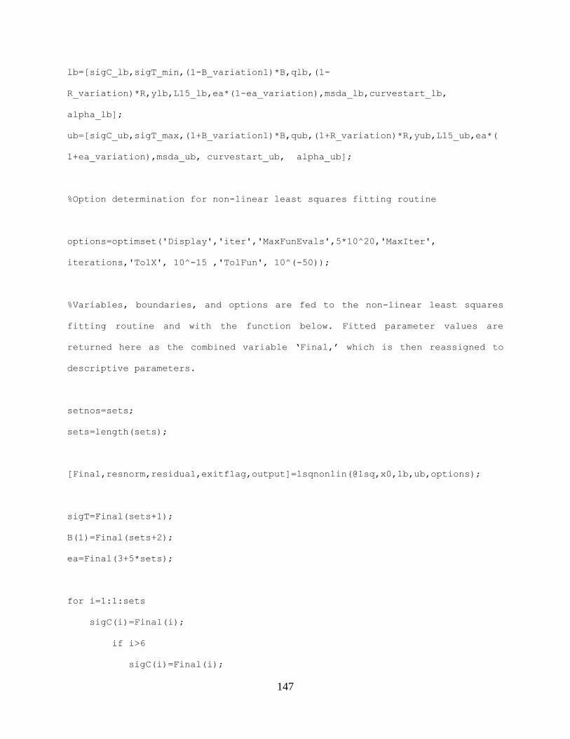
147
lb=[sigC_lb,sigT_min,(1-B_variation1)*B,qlb,(1-
R_variation)*R,ylb,L15_lb,ea*(1-ea_variation),msda_lb,curvestart_lb,
alpha_lb];
ub=[sigC_ub,sigT_max,(1+B_variation1)*B,qub,(1+R_variation)*R,yub,L15_ub,ea*(
1+ea_variation),msda_ub, curvestart_ub, alpha_ub];
%Option determination for non-linear least squares fitting routine
options=optimset('Display','iter','MaxFunEvals',5*10^20,'MaxIter',
iterations,'TolX', 10^-15 ,'TolFun', 10^(-50));
%Variables, boundaries, and options are fed to the non-linear least squares
fitting routine and with the function below. Fitted parameter values are
returned here as the combined variable ‘Final,’ which is then reassigned to
descriptive parameters.
setnos=sets;
sets=length(sets);
[Final,resnorm,residual,exitflag,output]=lsqnonlin(@lsq,x0,lb,ub,options);
sigT=Final(sets+1);
B(1)=Final(sets+2);
ea=Final(3+5*sets);
for i=1:1:sets
sigC(i)=Final(i);
if i>6
sigC(i)=Final(i);

148
end
q(i)=Final(i+2+1*sets);
R(i)=Final(i+2+2*sets);
yoff_off(i)=Final(i+2+3*sets);
L15(i)=Final(i+2+4*sets);
msda(i)=Final(1+3+5*sets);
cstart_off(i)=Final(i+3+6*sets);
alpha(i)=Final(i+3+7*sets);
end
for i=2:1:sets
B(i)=(q(i))*B(1);
end
for i=1:1:7
yoff(i)=cstart_off(i);
cstart(i)=yoff_dat(i);
end
for i=8:11
yoff(i)=cstart_off(i);
cstart(i)=yoff_dat(i);
end
%Parameters not marked as comments or followed by a semicolon will report their
final values in the MATLAB Command Window
sigC
sigT/sqrt(400)
B
ea
q
R
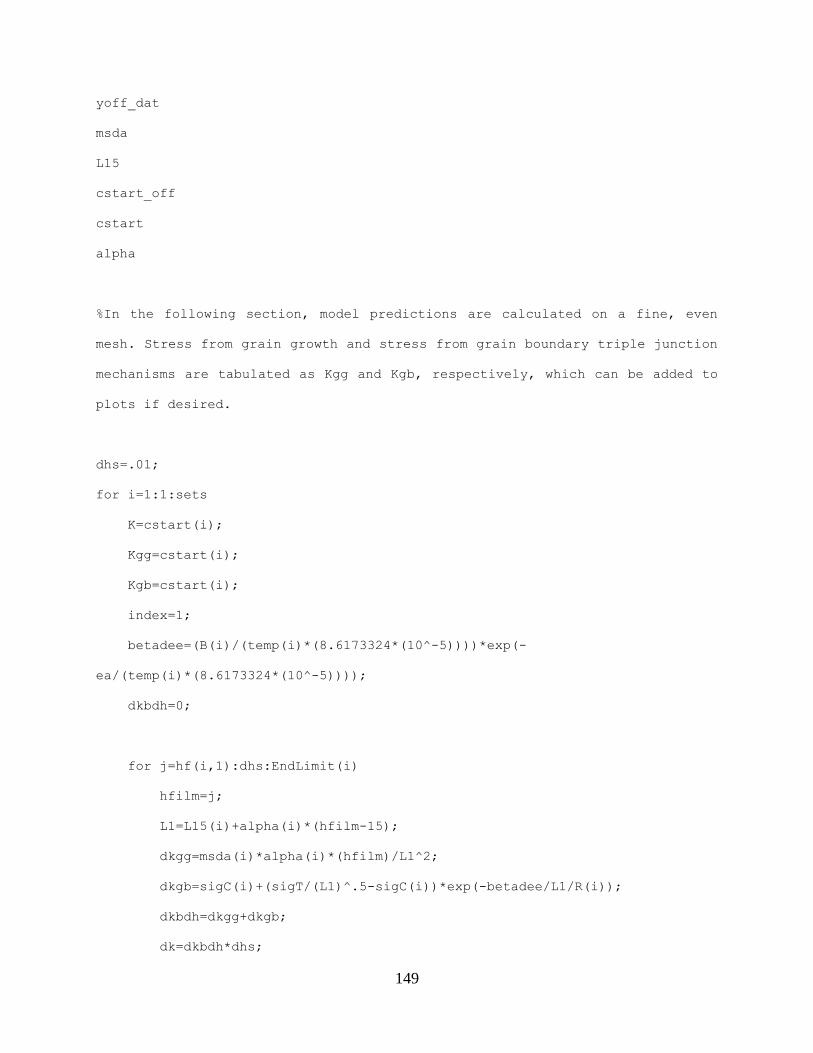
149
yoff_dat
msda
L15
cstart_off
cstart
alpha
%In the following section, model predictions are calculated on a fine, even
mesh. Stress from grain growth and stress from grain boundary triple junction
mechanisms are tabulated as Kgg and Kgb, respectively, which can be added to
plots if desired.
dhs=.01;
for i=1:1:sets
K=cstart(i);
Kgg=cstart(i);
Kgb=cstart(i);
index=1;
betadee=(B(i)/(temp(i)*(8.6173324*(10^-5))))*exp(-
ea/(temp(i)*(8.6173324*(10^-5))));
dkbdh=0;
for j=hf(i,1):dhs:EndLimit(i)
hfilm=j;
L1=L15(i)+alpha(i)*(hfilm-15);
dkgg=msda(i)*alpha(i)*(hfilm)/L1^2;
dkgb=sigC(i)+(sigT/(L1)^.5-sigC(i))*exp(-betadee/L1/R(i));
dkbdh=dkgg+dkgb;
dk=dkbdh*dhs;

150
K=K+dk;
int(index,i)=K+yoff(i);
moddk(index,i)=dk;
Kgg=Kgg+dkgg*dhs;
Kgb=Kgb+dkgb*dhs;
moddkgg(index,i)=Kgg+yoff(i);
moddkgb(index,i)=Kgb+yoff(i);
lhf(index,i)=j;
%Increase counter on every loop
index=index+1;
end
end
%For plotting the results, due to the large number of data sets, two plots are
generated when more than six data sets are fit.
figure1=figure('InvertHardcopy','off','Color',[1 1 1]); %%hold all;
axes1=axes('Parent',figure1,'FontSize',20,'FontName','Times New Roman');
xlim(axes1,[0 100]);
hold(axes1,'all');
xlabel({'Thickness (nm)'},'FontSize',24,'FontName','Times New Roman');
ylabel({'Stress thickness (N/m)'},'FontSize',24,'FontName','Times New Roman');
hold all;
for i=1:1:sets

151
datcolor(:,i)=[0,R(i)^.4+.2,(temp(i)-300)/(473-300)]; %Sets data colors
depending on growth rate and temperature
end
if sets<=6
for i=1:1:sets
plot(data(1:endcell(i),1,i),data(1:endcell(i),2,i),'Color',datcolor(:,
i),'Linewidth',2);hold all;
end
for i=1:1:sets
p=plot(lhf(5:find(lhf(:,i),1,'last'),i),int(5:find(lhf(:,i),1,'last'),
i),'b','LineWidth',1.5);hold all;
end
annotation('textbox',...
[0.767397521 0.78993198992 0.116301239 0.12594458438],...
'String',{'sigC = ' sigC,'sigT at 400nm = ' sigT/sqrt(400), 'Ea = ' ea,
'Bo = ' B(1) 'BD variation = ' B_variation2 'BDtot = '
(B./temp./(8.6173324*(10^-5))).*exp(-ea./temp./(8.6173324*(10^-5))) 'Lo = '
L15 'curvestart = ' cstart 'alpha = ' alpha 'msda = ' msda 'yoff = ' yoff 'R
= ' R 'T = ' temp});
hold off;
else
for i=1:1:6
plot(data(1:endcell(i),1,i),data(1:endcell(i),2,i),'Color',datcolor(:,
i),'Linewidth',2);hold all;
end
annotation('textbox',...
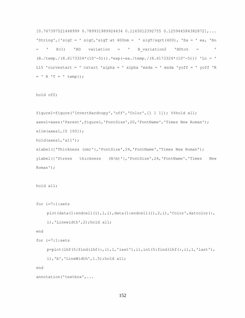
152
[0.767397521448999 0.789931989924434 0.1163012392755 0.125944584382872],...
'String',{'sigC = ' sigC,'sigT at 400nm = ' sigT/sqrt(400), 'Ea = ' ea, 'Bo
= ' B(1) 'BD variation = ' B_variation2 'BDtot = '
(B./temp./(8.6173324*(10^-5))).*exp(-ea./temp./(8.6173324*(10^-5))) 'Lo = '
L15 'curvestart = ' cstart 'alpha = ' alpha 'msda = ' msda 'yoff = ' yoff 'R
= ' R 'T = ' temp});
hold off;
figure1=figure('InvertHardcopy','off','Color',[1 1 1]); %%hold all;
axes1=axes('Parent',figure1,'FontSize',20,'FontName','Times New Roman');
xlim(axes1,[0 100]);
hold(axes1,'all');
xlabel({'Thickness (nm)'},'FontSize',24,'FontName','Times New Roman');
ylabel({'Stress thickness (N/m)'},'FontSize',24,'FontName','Times New
Roman');
hold all;
for i=7:1:sets
plot(data(1:endcell(i),1,i),data(1:endcell(i),2,i),'Color',datcolor(:,
i),'Linewidth',2);hold all;
end
for i=7:1:sets
p=plot(lhf(5:find(lhf(:,i),1,'last'),i),int(5:find(lhf(:,i),1,'last'),
i),'b','LineWidth',1.5);hold all;
end
annotation('textbox',...

153
[0.76739752144 0.78993198992 0.116301239 0.12594458438],'String',{'sigC = '
sigC,'sigT at 400nm = ' sigT/sqrt(400), 'Ea = ' ea, 'Bo = ' B(1) 'BD
variation = ' B_variation2 'BDtot = ' (B./temp./(8.6173324*(10^-5))).*exp(-
ea./temp./(8.6173324*(10^-5))) 'Lo = ' L15 'curvestart = ' cstart 'alpha =
' alpha 'msda = ' msda 'yoff = ' yoff 'R = ' R 'T = ' temp});
hold off;
end
save('lowmobdata1220out.mat','lhf');
save('lowmobfit1220out.mat','int');
end
%The following function accepts parameter values from the function above and
calculates the model predictions and the difference between the predictions and
the data, which becomes the quantity minimized by lsqnonlin.
function[FinalSigma]= lsq(x)
global sets temp hf L intstress cs setnos yoff_dat meshstress dataThickness
dataStress endcell
%Reassigns initial parameter values from the combined single vector fed to the
subroutine to more descriptive variables.
sigT=x(sets+1);
B(1)=x(sets+2);
ea=x(3+5*sets);

154
for i=1:1:sets
sigC(i)=x(i);
if i>6
sigC(i)=x(i);
end
q(i)=x(i+2+1*sets);
R(i)=x(i+2+2*sets);
yoff_off(i)=x(i+2+3*sets);
L15(i)=x(i+2+4*sets);
msda(i)=x(1+3+5*sets);
cstart_off(i)=x(i+3+6*sets);
alpha(i)=x(i+3+7*sets);
end
for i=1:1:7
yoff(i)=cstart_off(i);
cstart(i)=yoff_dat(i);
end
for i=8:11
yoff(i)=cstart_off(i);
cstart(i)=yoff_dat(i);
end
for i=2:1:sets
B(i)=(q(i))*B(1);
end
%Calculates the predicted cumulative stress from the model for each thickness
step using the most recent parameter values and determines the difference
between the model predictions and the data to be minimized.

155
intstress=zeros(size(hf));
cumintstress=intstress;
for i=1:1:sets
dh=hf(i,2)-hf(i,1);
K=cstart(i);
betadee=(B(i)/(temp(i)*(8.6173324*(10^-5))))*exp(-
ea/(temp(i)*(8.6173324*(10^-5))));
for j=1:1:find(hf(i,:),1,'last')
L1=L15(i)+(hf(i,j)-15)*alpha(i);
hfilm=hf(i,j);
dkbdh=sigC(i)+(sigT/(L1)^.5-sigC(i))*exp(-
betadee/L1/R(i))+msda(i)*(alpha(i)*hfilm)/(L1^2);
intstress(j,i)=dkbdh*dh;
K=K+intstress(j,i);
cs(j,i)=K;
cumintstress(j,i)=K+yoff(i);
end
end
FinalSigma=0;
for i=1:sets
FinalSigma=cat(1,FinalSigma,cumintstress(1:find(hf(i,:),1,'last'),i)-
(meshstress(1:find(hf(i,:),1,'last'),i)));
end
end

156
A.5 Program for zone II high mobility film stress
High mobility films with zone II microstructure are complicated not only by tensile stress from
grain boundary annihilation beneath the surface of the film, but also by atom transport through the
grain boundaries. This transport affects or even eliminates any stress gradient in the bulk of the
film, and it also changes the difference in chemical potential between the surface and the grain
boundary, which affects the compressive stress generation in newly deposited layers of the film.
The program below fitted stress thickness data deposited during experiments at a range of growth
rates and temperatures to a kinetic model which accounted for both stress from subsurface grain
growth and the effect of high mobility grain boundary transport on the compressive stress arising
from surface adatom insertion into the grain boundaries in addition to the tensile stress from grain
boundary formation. The coalescence regime was not treated here, but it was assumed that there
is rapid transport through the grain boundaries and tensile stress from grain growth contributed by
the full volume of the film outside of a small exclusion layer near the substrate. The results of this
fitting and further details can be found in chapter 6 and [6].
function [ ] = High_mobility_evaporated_Ni
%Non-linear least squares fitting program for low mobility zone II films
clear all
global sets temp L intstress cs hf setnos fstart yoff_dat meshstress
dataThickness dataStress endcell %Global variables are shared between all
functions in a program.
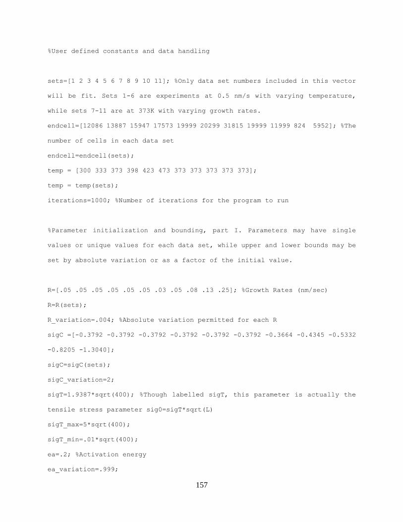
157
%User defined constants and data handling
sets=[1 2 3 4 5 6 7 8 9 10 11]; %Only data set numbers included in this vector
will be fit. Sets 1-6 are experiments at 0.5 nm/s with varying temperature,
while sets 7-11 are at 373K with varying growth rates.
endcell=[12086 13887 15947 17573 19999 20299 31815 19999 11999 824 5952]; %The
number of cells in each data set
endcell=endcell(sets);
temp = [300 333 373 398 423 473 373 373 373 373 373];
temp = temp(sets);
iterations=1000; %Number of iterations for the program to run
%Parameter initialization and bounding, part I. Parameters may have single
values or unique values for each data set, while upper and lower bounds may be
set by absolute variation or as a factor of the initial value.
R=[.05 .05 .05 .05 .05 .05 .03 .05 .08 .13 .25]; %Growth Rates (nm/sec)
R=R(sets);
R_variation=.004; %Absolute variation permitted for each R
sigC =[-0.3792 -0.3792 -0.3792 -0.3792 -0.3792 -0.3792 -0.3664 -0.4345 -0.5332
-0.8205 -1.3040];
sigC=sigC(sets);
sigC_variation=2;
sigT=1.9387*sqrt(400); %Though labelled sigT, this parameter is actually the
tensile stress parameter sig0=sigT*sqrt(L)
sigT_max=5*sqrt(400);
sigT_min=.01*sqrt(400);
ea=.2; %Activation energy
ea_variation=.999;
158
B=10; %Kinetic parameter (beta*D)_0, without temperature dependence included
B_variation1=15;%Factor variation allowed for B values from initial guess
B_variation2=.05; %Factor variation allowed between sets for B
msda=[1 1 1 1 1 1 1 1 1 1 1]*29; %Material parameter of the biaxial stress of
the film*the change in atom spacing from grain boundary elimination
msda=msda(sets);
msda_variation=.1;
fstart=15; %Film thickness at which fitting begins
dh=.05; %Interval between film thickness points for fitting (mesh size)
hex=7.5; %Height of exclusion zone near the substrate which does not contribute
to grain growth stress
hex_variation=7.5; %Absolute variation permitted for hex
alpha=[1 1 1 1 1 1 1 1 1 1 1]*.298; %Grain growth parameter determined
experimentally
alpha=alpha(sets);
alpha_variation=.298*.2; %Absolute variation permitted for alpha
%This section of code imports data from .csv files and organize it into a data
structure of film thickness, stress thickness, and data set number. The .csv
files are formatted as paired columns of film thickness in Angstroms and stress
thickness in N/m
name{1}='Yu Ni p5A range of T all copy.csv';
name{2}='373 K Yu Ni All copy.csv';
rawdata1=csvread(name{1},1,0,[1 0 20299 11]);
rawdata2=csvread(name{2},1,0,[1 0 31815 9]);
rawdata1(size(rawdata2),1)=0;
rawdata=[rawdata1 rawdata2];

159
data=zeros(min(endcell),2,length(sets));
for i=1:1:length(sets)
predata=rawdata(1:endcell(i),sets(i)*2-1:sets(i)*2);
n(2*i-1)=length(predata);
data(1:endcell(i),1,i)=predata(:,1)./10; %This converts the thickness data
from Angstroms to nm
data(1:endcell(i),2,i)=predata(:,2);
hfend(i)=floor(predata(find(predata(:,1),1, 'last'), 1)/10);
end
%Creates evenly spaced thickness values for each data set, from fstart to
hfend(i) with interval dh
hf=zeros(length(sets),max(hfend)-(fstart-1));
for i=1:1:length(sets)
index=1;
for j=1:dh:hfend(i)-(fstart-1)
hf(i,index)=(fstart-1)+j;
index=index+1;
end
end
%Creates separate stress and thickness structures for experimental data
interval=1;
for i=1:1:length(sets)
index=1;
for v=1:interval:n(2*i-1)

160
dataThickness(index,i)=data(v,1,i);
dataStress(index,i)=data(v,2,i);
index=index+1;
end
n(2*i)=ceil(n(2*i-1)/interval);
EndLimit(i)=dataThickness(n(2*i),i);
end
%Evenly spaced stress data is generated by averaging at evenly spaced thickness
points
for i=1:1:length(sets)
for j=1:1:find(hf(i,:), 1, 'last')
meshstress(j,i)=mean(data(data(1:endcell(i),1,i)>hf(i,j)-.51 &
data(1:endcell(i),1,i)<hf(i,j)+.51,2,i));
end
end
%The initial average stress value at film thickness fstart is set to yoff_dat
for i=1:1:length(sets)
x=(data(1:endcell(i),1,i)>fstart-2 & data(1:endcell(i),1,i)<fstart+2);
yoff_dat(i)=mean(data(x,2,i));
end
%Parameter initialization and bounding, part II. Absolute variation permitted
from experimental stress thickness at thickness fstart for initial model
prediction values. Because the stress thickness at the preceeding point
contributes to each new stress calculation, two small offsets are permitted.

161
The first, yoff, is the difference allowed between the first point of the model
prediction and the stress thickness data value at fstart. The second is the
difference between the stress thickness data value at fstart and the stress
thickness used to calculate the next point.
yoff=[1 1 1 1 1 1 1 1 1 1 1]*0;
yoff=yoff(sets);
yoff_variation=1;
cstart=[1 1 1 1 1 1 1 1 1 1 1]*0;
cstart=cstart(sets);
cstart_var=1;
for i=1:1:length(sets)
yoff(i)=0;
ylb(i)=yoff(i)-yoff_variation;
yub(i)=yoff(i)+yoff_variation;
cstart(i)=0;
curvestart_lb(i)=cstart(i)-cstart_var;
curvestart_ub(i)=cstart(i)+cstart_var;
q(i)=0;
qlb(i)=1-B_variation2;
qub(i)=1+B_variation2;
Rlb(i)=R(i)-R_variation;
Rub(i)=R(i)+R_variation;
sigC_ub(i)=sigC(i)+sigC_variation;
sigC_lb(i)=sigC(i)-sigC_variation;
L15(i)=10;
L15_lb(i)=5;
L15_ub(i)=15;
msda_lb(i)=msda(i)*(1-msda_variation);

162
msda_ub(i)=msda(i)*(1+msda_variation);
alpha_lb(i)=alpha(i)-alpha_variation;
alpha_ub(i)=alpha(i)+alpha_variation;
hex(i)=hex(1);
hex_lb(i)=hex(i)-hex_variation;
hex_ub(i)=hex(i)+hex_variation;
end
%Composite variables for initial values, upper bounds, and lower bounds must be
in the same order with the same length
x0=[sigC,sigT,B,q,R,yoff,L15, ea,msda,cstart,alpha,hex];
lb=[sigC_lb,sigT_min,(1-B_variation1)*B,qlb,(1-
R_variation)*R,ylb,L15_lb,ea*(1-ea_variation),msda_lb,curvestart_lb,
alpha_lb, hex_lb];
ub=[sigC_ub,sigT_max,(1+B_variation1)*B,qub,(1+R_variation)*R,yub,L15_ub,ea*(
1+ea_variation),msda_ub, curvestart_ub, alpha_ub, hex_ub];
setnos=sets;
sets=length(sets);
%Options for non-linear least squares fitting routine
options=optimset('Display','iter','MaxFunEvals',5*10^20,'MaxIter',
iterations,'TolX', 10^-15 ,'TolFun', 10^(-50));
%Variables, boundaries, and options are fed to the non-linear least squares
fitting routine and with the function below. Fitted parameter values are

163
returned here as the combined variable ‘Final,’ which is then reassigned to
descriptive parameters.
[Final,resnorm,residual,exitflag,output]=lsqnonlin(@lsq,x0,lb,ub,options);
sigT=Final(sets+1);
B(1)=Final(sets+2);
ea=Final(3+5*sets);
for i=1:1:sets
sigC(i)=Final(i);
if i>6
sigC(i)=Final(i);
end
q(i)=Final(i+2+1*sets);
R(i)=Final(i+2+2*sets);
yoff_off(i)=Final(i+2+3*sets);
L15(i)=Final(i+2+4*sets);
msda(i)=Final(1+3+5*sets);
cstart_off(i)=Final(i+3+6*sets);
alpha(i)=Final(i+3+7*sets);
hex(i)=Final(1+3+8*sets);
end
for i=2:1:sets
B(i)=(q(i))*B(1);
end
for i=1:1:7
range=dataThickness(1:endcell(i),i)>hex(i)-
.1&dataThickness(1:endcell(i),i)<hex(i)+.1;

164
hexy(i)=mean(dataStress(range,i)); %Stress thickness data value at the end
of the exlusion zone
yoff(i)=hexy(i)+yoff_off(i);
cstart(i)=yoff_dat(i)-hexy(i)+cstart_off(i);
end
for i=8:11
hexy(i)=hexy(7);
yoff(i)=hexy(i)+yoff_off(i);
cstart(i)=yoff_dat(i)-hexy(i)+cstart_off(i);
end
%Parameters and expressions not marked as comments or followed by a semicolon
will report their final values in the MATLAB Command Window
sigC
sigT/sqrt(400)
B./temp./(8.6173324*(10^-5))).*exp(-ea./temp./(8.6173324*(10^-5)))
ea
q
R
yoff
yoff_dat
yoff_off
msda
L15
cstart_off
cstart
alpha
hex

165
%In the following section, model predictions are calculated on a fine, even
mesh. Stress from grain growth and stress from grain boundary triple junction
mechanisms are tabulated as Kgg and Kgb, respectively, which can be added to
plots if desired.
dhs=.01;
for i=1:1:sets
K=cstart(i);
index=1;
betadee=(B(i)/(temp(i)*(8.6173324*(10^-5))))*exp(-
ea/(temp(i)*(8.6173324*(10^-5))));
dkbdh=0;
for j=hf(i,1):dhs:EndLimit(i)
if j-fstart < 0
dk=0;
L1=L15(i)+alpha(i)*(j-15);
hfilm=j;
dkbdh=0;
dkgg=0;
dkgb=0;
else
hfilm=j;
L1=L15(i)+alpha(i)*(hfilm-15);
dkgg=msda(i)*alpha(i)*(hfilm-hex(i))/L1^2;
dkgb=sigT/sqrt(L1)-betadee/R(i)/L1*(K/(hfilm-hex(i))-sigC(i));
dkbdh=dkgg+dkgb;
dk=dkbdh*dhs;
end

166
K=K+dk;
Kgg=Kgg+dkgg*dhs;
Kgb=Kgb+dkgb*dhs;
int(index,i) =K+yoff(i);
moddk(index,i)=dk;
moddkgg(index,i)= Kgg+yoff(i);
moddkgb(index,i)= Kgb+yoff(i);
lhf(index,i)=j;
%Increase counter on every loop
index=index+1;
end
end
%For plotting the results, due to the large number of data sets, two plots are
generated when more than six data sets are fit.
figure1=figure('InvertHardcopy','off','Color',[1 1 1]); %%hold all;
axes1=axes('Parent',figure1,'FontSize',20,'FontName','Times New Roman');
xlim(axes1,[0 100]);
hold(axes1,'all');
xlabel({'Thickness (nm)'},'FontSize',24,'FontName','Times New Roman');
ylabel({'Stress thickness (N/m)'},'FontSize',24,'FontName','Times New Roman');
hold all;
for i=1:1:sets
datcolor(:,i)=[0,R(i)^.4+.2,(temp(i)-300)/(473-300)]; %Sets data colors
depending on growth rate and temperature

167
end
if sets<=6
for i=1:1:sets
plot(data(1:endcell(i),1,i),data(1:endcell(i),2,i),'Color',datcolor(:,
i),'Linewidth',2);hold all;
end
for i=1:1:sets
p=plot(lhf(5:find(lhf(:,i),1,'last'),i),int(5:find(lhf(:,i),1,'last'),
i),'b','LineWidth',1.5);hold all;
end
annotation('textbox',...
[0.767397521 0.78993198992 0.116301239 0.12594458438],...
'String',{'sigC = ' sigC,'sigT at 400nm = ' sigT/sqrt(400), 'Ea = ' ea,
'Bo = ' B(1) 'BD variation = ' B_variation2 'BDtot = '
(B./temp./(8.6173324*(10^-5))).*exp(-ea./temp./(8.6173324*(10^-5))) 'Lo = '
L15 'curvestart = ' cstart 'alpha = ' alpha 'msda = ' msda 'yoff = ' yoff 'R
= ' R 'T = ' temp});
hold off;
else
for i=1:1:6
plot(data(1:endcell(i),1,i),data(1:endcell(i),2,i),'Color',datcolor(:,
i),'Linewidth',2);hold all;
end
annotation('textbox',...
[0.767397521448999 0.789931989924434 0.1163012392755 0.125944584382872],...

168
'String',{'sigC = ' sigC,'sigT at 400nm = ' sigT/sqrt(400), 'Ea = ' ea, 'Bo
= ' B(1) 'BD variation = ' B_variation2 'BDtot = '
(B./temp./(8.6173324*(10^-5))).*exp(-ea./temp./(8.6173324*(10^-5))) 'Lo = '
L15 'curvestart = ' cstart 'alpha = ' alpha 'msda = ' msda 'yoff = ' yoff 'R
= ' R 'T = ' temp});
hold off;
figure1=figure('InvertHardcopy','off','Color',[1 1 1]); %%hold all;
axes1=axes('Parent',figure1,'FontSize',20,'FontName','Times New Roman');
xlim(axes1,[0 100]);
hold(axes1,'all');
xlabel({'Thickness (nm)'},'FontSize',24,'FontName','Times New Roman');
ylabel({'Stress thickness (N/m)'},'FontSize',24,'FontName','Times New
Roman');
hold all;
for i=7:1:sets
plot(data(1:endcell(i),1,i),data(1:endcell(i),2,i),'Color',datcolor(:,i
),'Linewidth',2);hold all;
end
for i=7:1:sets
p=plot(lhf(5:find(lhf(:,i),1,'last'),i),int(5:find(lhf(:,i),1,'last'),i
),'b','LineWidth',1.5);hold all;
end
annotation('textbox',...
[0.76739752144 0.78993198992 0.116301239 0.12594458438],'String',{'sigC = '
sigC,'sigT at 400nm = ' sigT/sqrt(400), 'Ea = ' ea, 'Bo = ' B(1) 'BD
169
variation = ' B_variation2 'BDtot = ' (B./temp./(8.6173324*(10^-5))).*exp(-
ea./temp./(8.6173324*(10^-5))) 'Lo = ' L15 'curvestart = ' cstart 'alpha =
' alpha 'msda = ' msda 'yoff = ' yoff 'R = ' R 'T = ' temp});
hold off;
end
save('highmobdata.mat', 'lhf');
save('highmobfit.mat','int');
end
%The following function accepts parameter values from the function above and
calculates the model predictions and the difference between the predictions and
the data, which becomes the quantity minimized by lsqnonlin.
function[FinalSigma]= lsq(x)
global sets temp hf S L intstress cs setnos yoff_dat meshstress dataThickness
dataStress endcell
%Reassigns initial parameter values from the combined single vector to more
descriptive variables.
sigT=x(sets+1);
B(1)=x(sets+2);
ea=x(3+5*sets);
for i=1:1:sets
sigC(i)=x(i);

170
if i>6
sigC(i)=x(i);
end
q(i)=x(i+2+1*sets);
R(i)=x(i+2+2*sets);
yoff_off(i)=x(i+2+3*sets);
L15(i)=x(i+2+4*sets);
msda(i)=x(1+3+5*sets);
cstart_off(i)=x(i+3+6*sets);
alpha(i)=x(i+3+7*sets);
hex(i)=x(1+3+8*sets);
end
for i=2:1:sets
B(i)=(q(i))*B(1);
end
for i=1:1:7
range=dataThickness(1:endcell(i),i)>hex(i)-.1&
dataThickness(1:endcell(i),i)<hex(i)+.1;
hex_y(i)=mean(dataStress(range,i));
yoff(i)=hex_y(i)+yoff_off(i);
cstart(i)=yoff_dat(i)-hex_y(i)+cstart_off(i);
end
for i=8:11
hex_y(i)=hex_y(7);
yoff(i)=hex_y(i)+yoff_off(i);
cstart(i)=yoff_dat(i)-hex_y(i)+cstart_off(i);
end
171
%Calculates the predicted cumulative stress from the model for each thickness
step using the most recent parameter values and determines the difference
between the model predictions and the data to be minimized.
intstress=zeros(size(hf));
cumintstress=intstress;
for i=1:1:sets
dh=hf(i,2)-hf(i,1);
K=cstart(i);
betadee=(B(i)/(temp(i)*(8.6173324*(10^-5))))*exp(-
ea/(temp(i)*(8.6173324*(10^-5))));
for j=1:1:find(hf(i,:),1,'last')
L1=L15(i)+(hf(i,j)-15)*alpha(i);
hfilm=hf(i,j);
dkbdh=sigT/sqrt(L1)-betadee/R(i)/L1*(K/(hfilm-hex(i))-
sigC(i))+msda(i)*alpha(i)*(hfilm-hex(i))/L1^2;
intstress(j,i) = dkbdh*dh;
K=K+intstress(j,i);
cs(j,i)=K;
cumintstress(j,i)=K+yoff(i);
end
end
FinalSigma=0;
for i=1:sets
FinalSigma=cat(1,FinalSigma, cumintstress(1:find(hf(i,:),1,'last'),i)-
(meshstress(1:find(hf(i,:),1,'last'),i)));
end
end
172
References
[1] E. Chason, J. Shin, C.-H. Chen, A. Engwall, C. Miller, S. Hearne and L. Freund, Journal
of Applied Physics 115 (12), 123519 (2014).
[2] E. Chason, A. M. Engwall, C. M. Miller, C. H. Chen, A. Bhandari, S. K. Soni, S. J. Hearne,
L. B. Freund and B. W. Sheldon, Scripta Materialia 97, 33-36 (2015).
[3] A. Bhandari, B. W. Sheldon and S. J. Hearne, Journal of Applied Physics 101 (3), 033528
(2007).
[4] A. Engwall, Z. Rao and E. Chason, Materials & Design 110, 616-623 (2016).
[5] A. Engwall, Z. Rao and E. Chason, Journal of The Electrochemical Society 164 (13),
D828-D834 (2017).
[6] E. Chason, A. M. Engwall, Z. Rao and T. Nishimura, Journal of Applied Physics (in press
2018)