Embed Size (px)
Citation preview

BoS Chairman 35 : M.E. VLSI DESIGN - REGULATION 2007 - CURRICULUM
K.S.Rangasamy College of Technology - Autonomous Regulation
R 2007
Department Electronics and Communication
Engineering
Programme Code & Name 35 : M.E. VLSI Design

BoS Chairman 35 : M.E. VLSI DESIGN - REGULATION 2007 - CURRICULUM
K.S.Rangasamy College of Technology , Tiruchengode - 637215
Curriculum for the Programmes under Autonomous Scheme
Regulation R 2007
Department Department of Electronics and Communication Engineering
Programme Code & Name 35 : M.E. VLSI Design
Semester I
Course Code
Course Name Hours/ Week Credit Maximum marks
L T P C CA ES Total
THEORY
07350101C Applied Mathematics 3 1 0 4 50 50 100
07350102C Digital signal processing integrated circuits
3 1 0 4 50 50 100
07350103C Advanced Digital System Design
3 1 0 4 50 50 100
07350104C VLSI Design Techniques 4 0 0 4 50 50 100
07350105C Solid State Device Modeling And Simulation
4 0 0 4 50 50 100
07350106C Testing of VLSI Circuits 4 0 0 4 50 50 100
PRACTICAL
07350107P VLSI Design Laboratory I 0 0 3 2 50 50 100
Total 21 3 3 26 700
Semester II
Course Code
Course Name Hours/ Week Credit Maximum marks
L T P C CA ES Total
THEORY
07350201C Analysis and Design of Analog Integrated Circuits
4 0 0 4 50 50 100
07350202C Computer Aided Design of VLSI Circuits
4 0 0 4 50 50 100
07350203C VLSI Signal Processing 4 0 0 4 50 50 100
073502**E Elective I 3 0 0 3 50 50 100
073502**E Elective II 3 0 0 3 50 50 100
073502**E Elective III 3 0 0 3 50 50 100
PRACTICAL
07350207P VLSI Design Laboratory II 0 0 3 2 50 50 100
07350208P Technical seminar I 0 0 3 2 100 00 100
07350209P Technical report preparation & Presentation I
0 0 3 2 50 50 100
Total 21 0 9 27 900

BoS Chairman 35 : M.E. VLSI DESIGN - REGULATION 2007 - CURRICULUM
K.S.Rangasamy College of Technology , Tiruchengode - 637215
Curriculum for the Programmes under Autonomous Scheme
Regulation R 2007
Department Department of Electronics and Communication Engineering
Programme Code & Name 35 : M.E. VLSI Design
Semester III
Course Code
Course Name Hours/ Week Credit Maximum marks
L T P C CA ES Total
THEORY
073503**E Elective IV 3 0 0 3 50 50 100
073503**E Elective V 3 0 0 3 50 50 100
073503**E Elective VI 3 0 0 3 50 50 100
PRACTICAL
07350304P Project Work - Phase I 0 0 3 6 100 00 100
07350305P Technical Report Preparation & Presentation-II
0 0 3 2 100 00 100
Total 9 0 6 17 500
Semester IV
Course Code
Course Name Hours/ Week Credit Maximum marks
L T P C CA ES Total
07350401P Project Work - Phase II 0 0 30 20 50 50 100
Total 0 0 30 20 100

BoS Chairman 35 : M.E. VLSI DESIGN - REGULATION 2007 - CURRICULUM
K.S.Rangasamy College of Technology , Tiruchengode - 637215
Curriculum for the Programmes under Autonomous Scheme
Regulation R 2007
Department Department of Electronics and Communication Engineering
Programme Code & Name 35 : M.E. VLSI Design
List of Electives
Course Code
Course Name Hours/ Week Credit Maximum marks
L T P C CA ES Total
0735**41E CMOS VLSI Design 3 0 0 3 50 50 100
0735**42E VLSI Technology 3 0 0 3 50 50 100
0735**43E Neural Networks and Applications 3 0 0 3 50 50 100
0735**44E Design of Semiconductor Memories 3 0 0 3 50 50 100
0735**45E Computational Intelligent Techniques
3 0 0 3 50 50 100
0735**46E Advanced Microprocessors and Microcontrollers
3 0 0 3 50 50 100
0735**47E Low Power VLSI Design 3 0 0 3 50 50 100
0735**48E Analog VLSI Design 3 0 0 3 50 50 100
0735**49E ASIC Design 3 0 0 3 50 50 100
0735**50E Genetic Algorithms and their Applications
3 0 0 3 50 50 100
0735**51E Electromagnetic Interference and Compatibility in System Design
3 0 0 3 50 50 100
0735**52E Speech And Audio Signal Processing
3 0 0 3 50 50 100
0735**53E Reliability Engineering 3 0 0 3 50 50 100
0735**54E DSP Processor Architecture and Programming
3 0 0 3 50 50 100
0735**55E Physical Design of VLSI Circuits 3 0 0 3 50 50 100
0735**56E Digital Image Processing 3 0 0 3 50 50 100
0735**57E Computer Architecture and Parallel Processing
3 0 0 3 50 50 100

BoS Chairman 35 : M.E. VLSI DESIGN - REGULATION 2007 - SYLLABUS
K.S.Rangasamy College of Technology - Autonomous Regulation R 2007
Department Electronics & Communication
Engineering Programme Code & Name 35 : M.E. VLSI Design
Semester I
Course Code Course Name Hours/ Week Credit Maximum Marks
L T P C CA ES Total
07350101S APPLIED MATHEMATICS 3 1 0 4 50 50 100
Objective(s) To develop efficient algorithms for solving numerical methods, to acquire skills in handling situation involving random variable. To learn the basics and gained the skill for specialized studies and research.
1 LINEAR ALGEBRAIC EQUATION AND EIGEN VALUE PROBLEMS
Total Hrs 12
System of equations- Solution by Gauss Elimination, Gauss-Jordan and LU decomposition method- Jacobi, Gauss-Seidal iteration method- Eigen values of a matrix by Jacobi and Power method.
2 WAVE EQUATION Total Hrs 12
Solution of initial and boundary value problems- Characteristics- D‘Alembert‘s Solution - Significance of characteristic curves - Laplace transform solutions for displacement in a long string - a long string under its weight - a bar with prescribed force on one end- free vibrations of a string.
3 SPECIAL FUNCTIONS Total Hrs 12
Bessel‘s equation - Bessel Functions- Legendre‘s equation - Legendre polynomials - Rodrigue‘s formula - Recurrence relations- generating functions and orthogonal property for Bessel functions - Legendre polynomials.
4 RANDOM VARIABLES Total Hrs 12
One dimensional Random Variable - Moments and MGF – Binomial, Poisson, Geometrical, Normal Distributions- Two dimensional Random Variables – Marginal and Conditional Distributions – Covariance and Correlation Coefficient - Functions of Two dimensional random variable
5 QUEUEING THEORY Total Hrs 12
Single and Multiple server Markovian queueing models - Steady state system size probabilities – Little‘s formula - Priority queues - M/G/1 queueing system – P.K. formula.
Total hours to be taught 60
Reference(s) :
1 Sankara Rao.K. ―Introduction to Partial Differential Equation ―, PHI, 1995.
2 Taha. H.A., ―Operations Research- An Introduction ― 6th Edition, PHI, 1997.
3 Jain M.K. Iyengar, S.R.K. & Jain R.K., ―International Methods for Scientific and Engineering Computation‖, New Age International (P) Ltd, Publlishers 2003.

BoS Chairman 35 : M.E. VLSI DESIGN - REGULATION 2007 - SYLLABUS
K.S.Rangasamy College of Technology - Autonomous Regulation R 2007
Department Electronics & Communication
Engineering Programme Code & Name 35 : M.E. VLSI Design
Semester I
Course Code Course Name Hours/ Week Credit Maximum Marks
L T P C CA ES Total
07350102C DIGITAL SIGNAL PROCESSING INTEGRATED CIRCUITS
3 1 0 4 50 50 100
Objective(s) To study DSP system design & CMOS technologies, DFT & FFT computation. To introduce the architecture of synthesis of DSP
1 DSP INTEGRATED CIRCUITS AND VLSI CIRCUIT TECHNOLOGIES
Total Hrs 12
Standard digital signal processors, Application specific IC‘s for DSP, DSP systems, DSP system design, Integrated circuit design. MOS transistors, MOS logic, VLSI process technologies, Trends in CMOS technologies.
2 DIGITAL SIGNAL PROCESSING Total Hrs 12
Digital signal processing, Sampling of analog signals, Selection of sample frequency, Signal-processing systems, Frequency response, Transfer functions, Signal flow graphs, Filter structures, Adaptive DSP algorithms, DFT-The Discrete Fourier Transform, FFT-The Fast Fourier Transform Algorithm, Image coding, Discrete cosine transforms.
3 DIGITAL FILTERS AND FINITE WORD LENGTH EFFECTS Total Hrs 12
FIR filters, FIR filter structures, FIR chips, IIR filters, Specifications of IIR filters, Mapping of analog transfer functions, Mapping of analog filter structures, Multirate systems, Interpolation with an integer factor L, Sampling rate change with a ratio L/M, Multirate filters. Finite word length effects -Parasitic oscillations, Scaling of signal levels, Round-off noise, measuring round-off noise, Coefficient sensitivity, Sensitivity and noise.
4 DSP ARCHITECTURES AND SYNTHESIS OF DSP ARCHITECTURES
Total Hrs 12
DSP system architectures, Standard DSP architecture, Ideal DSP architectures, Multiprocessors and multicomputers, Systolic and Wave front arrays, Shared memory architectures. Mapping of DSP algorithms onto hardware, Implementation based on complex PEs, Shared memory architecture with Bit – serial PEs.
5 ARITHMETIC UNITS AND INTEGRATED CIRCUIT DESIGN Total Hrs 12
Conventional number system, Redundant Number system, Residue Number System, Bit-parallel and Bit-Serial arithmetic, Basic shift accumulator, Reducing the memory size, Complex multipliers, Improved shift-accumulator. Layout of VLSI circuits, FFT processor, DCT processor and Interpolator as case studies.
Total hours to be taught 60
Reference(s) :
1 Lars Wanhammer, ―DSP Integrated Circuits‖, Academic press, New York 1999.
2 A.V.Oppenheim et.al, ‗Discrete-time Signal Processing‘ Pearson education, 2000.
3 Emmanuel C. Ifeachor, Barrie W. Jervis, ―Digital signal processing – A practical approach‖, Second edition, Pearson education, Asia 2001.

BoS Chairman 35 : M.E. VLSI DESIGN - REGULATION 2007 - SYLLABUS
K.S.Rangasamy College of Technology - Autonomous Regulation R 2007
Department Electronics & Communication
Engineering Programme Code & Name 35 : M.E. VLSI Design
Semester I
Course Code Course Name Hours/ Week Credit Maximum Marks
L T P C CA ES Total
07350103C
ADVANCED DIGITAL SYSTEM DESIGN (Common to M.E. (Applied Electronics, VLSI Design)
3 1 0 4 50 50 100
Objective(s) To learn how to design programmable logic circuits, logic synthesis compiler based on VHDL. To determine the types of fault that occur in digital circuits.
1 SEQUENTIAL LOGIC OPTIMIZATION Total Hrs 12
Sequential Circuit Optimization Using State Based Models, Sequential Circuit Optimization Using Network Models, Implicit Finite State machine Traversal Methods, Testability Considerations for Synchronous Circuits.
2 ASYNCHRONOUS FINITE STATE MACHINES Total Hrs 12
Scope, Asynchronous Analysis, Design of Asynchronous Machines, Cycle and Races, Plotting and Reading the Excitation Map, Hazards, Essential Hazards Map Entered Variable, MEV Approaches to Asynchronous Design, Hazards in Circuit Developed by MEV Method.
3 DIGITAL SYSTEM TESTING Total Hrs 12
Fault Models, Fault Equivalence, Fault Location, Fault Dominance, Single and Multiple Stack Faults, Testing for Single Stack Faults, Algorithms, Random test Generation, Adhoc Design for Testability Techniques, Classical Scan Designs, Boundary Scan Standards, Built-In-Self-Test, Test Pattern Generation, BIST Architecture examples.
4 HIGH SPEED DIGITAL DESIGN Total Hrs 12
Frequency, Time and Distance, Capacitance and Inductance Effects, High Speed Properties of Logical Gates, Speed And Power, Measurement Techniques, Rise Time and Bandwidth of Oscilloscope probes, Self Inductance , Signal pickup and loading effects of probes, clock distribution, clock skew and methods to reduce skew, Controlling crosstalk on clock lines, Delay adjustments, Clock oscillators and clockjitter.
5 SYSTEM DESIGN USING VHDL Total Hrs 12
Specification of combinational systems using VHDL, Basic language element of VHDL, Types of Modeling, Design of serial adder with accumulator, State graph for Control network, Design of Binary Multiplier and Binary Divider, Flip-Flops, Registers, Counters, Sequential Machines, Combinational Logic Circuits.
Total hours to be taught 60
Reference(s) :
1 Fletcher .An Engineering Approach to Digital Design, PHI 2004.
2 Parag K Lala ,Digital Circuit Testing And Testability, Academic 1997.
3 Miron Abramovici et. al , Digital System Testing And Testable Design, Jaico Publishing House 2001.
4 Howard Johnson and Martin Graham, High Speed Digital Design : Handbook of Black Magic, PHI PTR.

BoS Chairman 35 : M.E. VLSI DESIGN - REGULATION 2007 - SYLLABUS
K.S.Rangasamy College of Technology - Autonomous Regulation R 2007
Department Electronics & Communication
Engineering Programme Code & Name 35 : M.E. VLSI Design
Semester I
Course Code Course Name Hours/ Week Credit Maximum Marks
L T P C CA ES Total
07350104C VLSI DESIGN TECHNIQUES 4 0 0 4 50 50 100
Objective(s) To learn the CMOS processing technology and basic CMOS circuits, CMOS transistor theory and logic design. To study about verilog HDL programming.
1 VLSI DESIGN PROCESS & MOS TRANSISTOR THEORY AND PROCESS TECHNOLOGY
Total Hrs 12
VLSI Design Process – Architectural Design – Logical Design – Physical Design – Layout Styles –Full custom, Semicustom approaches. NMOS and PMOS transistors, Threshold voltage- Body effect- Design equations- Second order effects. MOS models and small signal AC characteristics. Basic CMOS technology.
2 INVERTERS AND LOGIC GATES Total Hrs 12
NMOS and CMOS Inverters, Stick diagram, Inverter ratio, DC and transient characteristics , switching times, Super buffers, Driving large capacitance loads, CMOS logic structures , Transmission gates, Static CMOS design, dynamic CMOS design.
3 CIRCUIT CHARACTERISATION & PERFORMANCE ESTIMATION
Total Hrs 12
Resistance estimation, Capacitance estimation, Inductance, switching characteristics, transistor sizing, power dissipation and design margining. Charge sharing .Scaling.
4 VLSI SYSTEM COMPONENTS CIRCUITS Total Hrs 12
Multiplexers, Decoders, comparators, priority encoders, Shift registers. Arithmetic circuits – Ripple carry adders, Carry look ahead adders, High-speed adders, Multipliers
5 VERILOG HARDWARE DESCRIPTION LANGUAGE Total Hrs 12
Overview of digital design with Verilog HDL, hierarchical modelling concepts, modules and port definitions, gate level modelling, data flow modelling, behavioral modelling, task & functions, Test Bench.
Total hours to be taught 60
Reference(s) :
1 Jan M Rabaey, ― Digital Integrated Circuits‖ Prentice Hall of India, 2002.
2 Sung-Mo Kang and Yusuf Leblebici, ―CMOS Digital Integrated Circuits- Analysis and Design‖,Tata McGraw Hill,2003
3 Neil H.E. Weste and Kamran Eshraghian, Principles of CMOS VLSI Design, Pearson Education ASIA, 2nd edition, 2000.
4 John P.Uyemura ―Introduction to VLSI Circuits and Systems‖, John Wiley & Sons, Inc., 2002.
5 J.Bhasker, B.S.Publications, ―A Verilog HDL Primer‖, 2nd Edition, 2001.
6 Pucknell, ―Basic VLSI Design‖, Prentice Hall of India Publication, 1995.
7 Wayne Wolf ―Modern VLSI Design System on chip. Pearson Education.2002.

BoS Chairman 35 : M.E. VLSI DESIGN - REGULATION 2007 - SYLLABUS
K.S.Rangasamy College of Technology - Autonomous Regulation R 2007
Department Electronics & Communication
Engineering Programme Code & Name 35 : M.E. VLSI Design
Semester I
Course Code Course Name Hours/ Week Credit Maximum Marks
L T P C CA ES Total
07350105C SOLID STATE DEVICE MODELING AND SIMULATION
4 0 0 4 50 50 100
Objective(s) It gives overall idea about solid state devices and it‘s parameters, it deals the modeling technique and different models used for the implementation of circuits using solid state devices
1 BASIC SEMICONDUCTOR PHYSICS Total Hrs 12
Quantum Mechanical Concepts, Carrier Concentration, Transport Equation, Band gap, Mobility and Resistivity, Carrier Generation and Recombination, Avalanche Process, Noise Sources. Diodes: Forward and Reverse biased junctions – Reverse bias breakdown – Transient and AC conditions -– Static and Dynamic behavior- Small and Large signal models – SPICE model for a Diode – Temperature and Area effects on Diode Model Parameters.
2 BIPOLAR DEVICE MODELING Total Hrs 12
Transistor Models: BJT – Transistor Action – Minority carrier distribution and Terminal currents - Switching- Eber - Molls and Gummel Poon Model, SPICE modeling - temperature and area effects.
3 MOSFET MODELING Total Hrs 12
MOS Transistor – NMOS, PMOS – MOS Device equations - Threshold Voltage – Second order effects - Temperature Short Channel and Narrow Width Effect, Models for Enhancement, Depletion Type MOSFET, CMOS Models in SPICE.
4 PARAMETER MEASUREMENT Total Hrs 12
Bipolar Junction Transistor Parameter – Static Parameter Measurement Techniques – Large signal parameter Measurement Techniques, Gummel Plots, MOSFET: Long and Short Channel Parameters, Measurement of Capacitance.
5 OPTOELECTRONIC DEVICE MODELING Total Hrs 12
Static and Dynamic Models, Rate Equations, Numerical Technique, Equivalent Circuits, Modeling of LEDs, Laser Diode and Photo detectors.
Total hours to be taught 60
Reference(s) :
1 Ben.G..Streetman, ―Solid State Devices‖, Prentice Hall , 1997.
2 Giuseppe Massobrio and Paolo Antogentti, ―Semiconductor Device Modeling with SPICE‖ 2nd Edition, McGraw-Hill Inc, New York, 1993.
3 Tyagi M.S. ―Introduction to Semiconductor Devices‖, 2 nd Edition Mc Graw Hill, New York,1981.
BoS Chairman 35 : M.E. VLSI DESIGN - REGULATION 2007 - SYLLABUS
K.S.Rangasamy College of Technology - Autonomous Regulation R 2007
Department Electronics & Communication
Engineering Programme Code & Name 35 : M.E. VLSI Design
Semester I
Course Code Course Name Hours/ Week Credit Maximum Marks
L T P C CA ES Total
07350106C TESTING OF VLSI CIRCUITS 4 0 0 4 50 50 100
Objective(s) Complex digital systems in single chips, must be verify to ensure that they are functioning correctly. Testing of VLSI circuits deals with the nuts and bolts of such technique used verify the system in chip.
1 Total Hrs 12
Introduction to Testing - Faults in digital circuits - Modeling of faults - Logical Fault Models - Fault detection - Fault location - Fault dominance - Logic Simulation - Types of simulation - Delay models - Gate level Event-driven simulation.
2 Total Hrs 12
Test generation for combinational logic circuits - Testable combinational logic circuit design - Test generation for sequential circuits - design of testable sequential circuits.
3 Total Hrs 12
Design for Testability - Ad-hoc design - Generic scan based design - Classical scan based design - System level DFT approaches.
4 Total Hrs 12
Built-In Self Test - Test pattern generation for BIST - Circular BIST – BIST Architectures - Testable Memory Design - Test algorithms - Test generation for Embedded RAMs.
5 Total Hrs 12
Logic Level Diagnosis - Diagnosis by UUT reduction - Fault Diagnosis for Combinational Circuits - Self-checking design - System Level Diagnosis.
Total hours to be taught 60
Reference(s) :
1 M. Abramovici, M.A. B reuer and A.D. Friedman, "Digital Systems and Testable Design", Jaico Publishing House, 2002.
2 P.K. Lala, "Digital Circuit Testing and Testability", Academic Press, 2002
3 M.L. Bushnell and V.D. Agrawal, "Essentials of Electronic Testing for Digital, Memory and Mixed-Signal VLSI Circuits", Kluwar Academic Publishers, 2002.

BoS Chairman 35 : M.E. VLSI DESIGN - REGULATION 2007 - SYLLABUS
K.S.Rangasamy College of Technology - Autonomous Regulation R 2007
Department Electronics & Communication
Engineering Programme Code & Name 35 : M.E. VLSI Design
Semester I
Course Code Course Name Hours/ Week Credit Maximum Marks
L T P C CA ES Total
07350107C VLSI DESIGN LABORATORY I 0 0 3 2 50 50 100
LIST OF EXPERIMENTS
1. Modeling of Sequential Digital system using VHDL. 2. Modeling of Sequential Digital system using Verilog. 3. Writing Test Benches Using Verilog / VHDL 4. Design and Implementation of ALU using FPGA. 5. Simulation of NMOS and CMOS circuits using SPICE. 6. Design of Static and Dynamic Logic Circuits 7. Modeling of MOSFET using C. 8. Implementation of FFT, Digital Filters. 9. Implementation of DSP algorithms using software package. 10. Implementation of MAC Unit using FPGA.

BoS Chairman 35 : M.E. VLSI DESIGN - REGULATION 2007 - SYLLABUS
K.S.Rangasamy College of Technology - Autonomous Regulation R 2007
Department Electronics & Communication
Engineering Programme Code & Name 35 : M.E. VLSI Design
Semester II
Course Code Course Name Hours/ Week Credit Maximum Marks
L T P C CA ES Total
07350201S ANALYSIS AND DESIGN OF ANALOG INTEGRATED CIRCUITS
4 0 0 4 50 50 100
Objective(s)
It depend heavily on the utilization of suitable models for integrated circuit components, analyze the various circuit configuration n encountered in Linear Integrated Circuits and Explore several applications of opamps to illustrate their versatility in analog circuit and system design.
1 MODELS FOR INTEGRATED CIRCUIT ACTIVE DEVICES
Total Hrs 12
Depletion region of a pn junction – large signal behavior of bipolar transistors- small signal model of bipolar transistor- large signal behavior of MOSFET- small signal model of the MOS transistors- short channel effects in MOS transistors – weak inversion in MOS transistors- substrate current flow in MOS transistor.
2 CIRCUIT CONFIGURATION FOR LINEAR IC Total Hrs 12
Current sources, Analysis of difference amplifiers with active load using BJT and FET, supply and temperature independent biasing techniques, voltage references. Output stages: Emitter follower, source follower and Push pull output stages.
3 OPERATIONAL AMPLIFIERS Total Hrs 12
Analysis of operational amplifiers circuit, slew rate model and high frequency analysis, Frequency response of integrated circuits: Single stage and multistage amplifiers, Operational amplifier noise
4 ANALOG MULTIPLIER AND PLL Total Hrs 12
Analysis of four quadrant and variable trans conductance multiplier, voltage controlled oscillator, closed loop analysis of PLL, Monolithic PLL design in integrated circuits: Sources of noise- Noise models of Integrated-circuit Components – Circuit Noise Calculations – Equivalent Input Noise Generators – Noise Bandwidth – Noise Figure and Noise Temperature.
5 ANALOG DESIGN WITH MOS TECHNOLOGY Total Hrs 12
MOS Current Mirrors – Simple, Cascode, Wilson and Widlar current source – CMOS Class AB output stages – Two stage MOS Operational Amplifiers, with Cascode, MOS Telescopic-Cascode Operational Amplifier – MOS Folded Cascode and MOS Active Cascode Operational Amplifiers.
Total hours to be taught 60
Reference(s) :
1 Gray, Meyer, Lewis, Hurst, ―Analysis and design of Analog IC‘s‖, 4th
Edition, Wiley International, 2002.
2 Behzad Razavi, ―Design of Analog CMOS Integrated Circuits‖, S.Chand and company ltd, 2000
3 Nandita Dasgupata, Amitava Dasgupta, ‖Semiconductor Devices, Modelling and Technology‖, Prentice Hall of Indiapvt.ltd,2004.
BoS Chairman 35 : M.E. VLSI DESIGN - REGULATION 2007 - SYLLABUS
K.S.Rangasamy College of Technology - Autonomous Regulation R 2007
Department Electronics & Communication
Engineering Programme Code & Name 35 : M.E. VLSI Design
Semester II
Course Code Course Name Hours/ Week Credit Maximum Marks
L T P C CA ES Total
07350202C COMPUTER AIDED DESIGN OF VLSI CIRCUITS
4 0 0 4 50 50 100
Objective(s) To know about the algorithms that are used inside VLSI design automation tools and how these tools are used to design a VLSI chip
1 Total Hrs 12
Introduction to VLSI Design methodologies - Review of Data structures and algorithms - Review of VLSI Design automation tools - Algorithmic Graph Theory and Computational Complexity - Tractable and Intractable problems - general purpose methods for combinatorial optimization.
2 Total Hrs 12
Layout Compaction - Design rules - problem formulation - algorithms for constraint graph compaction - placement and partitioning - Circuit representation - Placement algorithms - partitioning
3 Total Hrs 12
Floor planning concepts - shape functions and floorplan sizing - Types of local routing problems - Area routing - channel routing - global routing - algorithms for global routing.
4 Total Hrs 12
Simulation - Gate-level modeling and simulation - Switch-level modeling and simulation - Combinational Logic Synthesis - Binary Decision Diagrams - Two Level Logic Synthesis.
5 Total Hrs 12
High level Synthesis - Hardware models - Internal representation - Allocation - assignment and
scheduling - Simple scheduling algorithm - Assignment problem – High level transformations.
Total hours to be taught 60
Reference(s) :
1 S.H. Gerez, "Algorithms for VLSI Design Automation", John Wiley & Sons,2002
2 N.A. Sherwani, "Algorithms for VLSI Physical Design Automation", Kluwar Academic Publishers, 2002.
3 Drechsler,R., Evolutionary Algorithms for VLSI CAD, Kluwer Academic Publishers, Boston, 1998.
BoS Chairman 35 : M.E. VLSI DESIGN - REGULATION 2007 - SYLLABUS
K.S.Rangasamy College of Technology - Autonomous Regulation R 2007
Department Electronics & Communication
Engineering Programme Code & Name 35 : M.E. VLSI Design
Semester II
Course Code Course Name Hours/ Week Credit Maximum Marks
L T P C CA ES Total
07350203C VLSI SIGNAL PROCESSING 4 0 0 4 50 50 100
Objective(s) To study the transformations for high speed using pipelining, returning and parallel processing techniques and experience on power reduction transformation for supply voltage reduction, capacitance reduction. To learn area reduction using folding techniques
1 INTRODUCTION TO DSP SYSTEMS Total Hrs 12
Introduction To DSP Systems -Typical DSP algorithms; Iteration Bound – data flow graph representations, loop bound and iteration bound, Longest path Matrix algorithm; Pipelining and parallel processing – Pipelining of FIR digital filters, parallel processing, pipelining and parallel processing for low power.
2 RETIMING, FOLDING AND UNFOLDING Total Hrs 12
Retiming - definitions and properties Retiming techniques; Unfolding – an algorithm for Unfolding, properties of unfolding, sample period reduction and parallel processing application; Folding – Folding transformation – Register minimizing techniques – Register minimization in folded architectures.
3 FAST CONVOLUTION Total Hrs 12
Fast convolution – Cook-Toom algorithm, modified Cook-Took algorithm – Winograd Algorithm, Iterated Convolution – Cyclic Convolution; Pipelined and parallel recursive and adaptive filters – inefficient/efficient single channel interleaving, Look- Ahead pipelining in first- order IIR filters, Look-Ahead pipelining with power-of-two decomposition parallel processing of IIR filters, combined pipelining and parallel processing of IIR filters, pipelined adaptive digital filters, relaxed look-ahead, pipelined LMS adaptive filter.
4 BIT-LEVEL ARITHMETIC ARCHITECTURES Total Hrs 12
Bit-Level Arithmetic Architectures- parallel multipliers with sign extension, parallel carry-ripple array multipliers, parallel carry-save multiplier, 4x 4 bit Baugh- Wooley carry-save multiplication tabular form and implementation, design of Lyon‘s bit-serial multipliers using Horner‘s rule, bit-serial FIR filter, CSD representation, CSD multiplication using Horner‘s rule for precision improvement.
5 PROGRAMMING DIGITAL SIGNAL PROCESSORS Total Hrs 12
Synchronous, Wave and asynchronous pipelining- synchronous pipelining and clocking styles, clock skew in edge-triggered single-phase clocking, two-phase clocking, wave pipelining, asynchronous pipelining bundled data versus dual rail protocol; Programming Digital Signal Processors – generalarchitecture with important features; Low power Design – needs for low power VLSI chips, charging and discharging capacitance, short-circuit current of an inverter, CMOS leakage current, basic principles of low power design.
Total hours to be taught 60
Reference(s) :
1 Keshab K.Parhi, ―VLSI Digital Signal Processing systems, Design and implementation‖, Wiley, Inter Science, 1999.
2 Gary Yeap, ―Practical Low Power Digital VLSI Design‖, Kluwer Academic Publishers, 1998.

BoS Chairman 35 : M.E. VLSI DESIGN - REGULATION 2007 - SYLLABUS
K.S.Rangasamy College of Technology - Autonomous Regulation R 2007
Department Electronics & Communication
Engineering Programme Code & Name 35 : M.E. VLSI Design
Semester II
Course Code Course Name Hours/ Week Credit Maximum Marks
L T P C CA ES Total
07350207C VLSI DESIGN LABORATORY II
0 0 3 2 50 50 100
LIST OF EXPERIMENTS
1. Implementation of 8 Bit ALU in FPGA / CPLD. 2. Implementation of 4 Bit Sliced processor in FPGA / CPLD. 3. Implementation of Elevator controller using embedded microcontroller. 4. Implementation of Alarm clock controller using embedded microcontroller. 5. Implementation of model train controller using embedded microcontroller. 6. System design using PLL.

BoS Chairman 35 : M.E. VLSI DESIGN - REGULATION 2007 - SYLLABUS
K.S.Rangasamy College of Technology - Autonomous Regulation R 2007
Department Electronics & Communication
Engineering Programmes Code &
Name 35 : M.E. VLSI Design
Semester II
Course Code Course Name Hours / Week Credit Maximum Marks
L T P C CA ES Total
07350209P TECHNICAL REPORT PREPARATION & PRESENTATION I
0 0 3 2 100 00 100
Objective(s) To provide exposure to the students to refer, read and review the research articles in referred journals and conference proceedings. To Improve the technical report writing and presentation skills of the students.
Methodology
Each student is allotted to a faculty of the department by the HOD
By mutual discussions, the faculty guide will assign a topic in the general / subject area to the student.
The students have to refer the Journals and Conference proceedings and collect the published literature.
The student is expected to collect at least 20 such Research Papers published in the last 5 years.
Using OHP/Power Point, the student has to make presentation for 15-20 minutes followed by 10 minutes discussion.
The student has make two presentations, one at the middle and the other near the end of the semester.
The student has to write a Technical Report for about 30-50 pages (Title page, One page Abstract, Review of Research paper under various subheadings, Concluding Remarks and List of References). The technical report has to be submitted to the HOD one week before the final presentation, after the approval of the faculty guide.
Execution
Week Activity
I Allotment of Faculty Guide by the HoD
II Finalizing the topic with the approval of Faculty Guide
III-IV Collection of Technical papers
V-VI Mid semester presentation
VII-VIII Report writing
IX Report submission
X-XI Final presentation
Evaluation
100% by Continuous Assessment 3 Hrs/week and 2 credits
Component Weightage
Phase -I Presentation 25 %
Phase - II Presentation 25 %
Report Preparation and Submission 30 %
Final Presentation 20 %
Total 100 %

BoS Chairman 35 : M.E. VLSI DESIGN - REGULATION 2007 - SYLLABUS
K.S.Rangasamy College of Technology - Autonomous Regulation R 2007
Department Electronics & Communication
Engineering Programme Code & Name 35 : M.E. VLSI Design
ELECTIVES
Course Code Course Name Hours/ Week Credit Maximum Marks
L T P C CA ES Total
0735**41E CMOS VLSI DESIGN 3 0 0 3 50 50 100
Objective(s) To learn the CMOS processing technology and basic CMOS circuits, CMOS transistor theory and to learn logic design.
1 MOS TRANSISTOR THEORY Total Hrs 9
Introduction to I.C Technology. Basic MOS transistors. Threshold Voltage. Body effect. Basic D.C. Equations. Second order effects. MOS models. Small signal A.C characteristics. The complementary CMOS inverter. DC characteristics. Static Load MOS inverters. The differential inverters. Transmission gate.
2 CMOS PROCESSING TECHNOLOGY Total Hrs 9
Silicon semiconductor technology. Wafer processing, Oxidation, epitaxy, deposition, Ion implantation. CMOS technology. nwell, pwell process. Silicon on insulator. CMOS process enhancement. Interconnect and circuit elements. Layout design rules. Latchup.
3 CIRCUIT CHARACTERISTICS AND PERFORMANCE ESTIMATION
Total Hrs 9
Resistance estimation. Capacitance estimation. MOS capacitor characteristics. Device capacitances. Diffusion capacitance. SPICE modeling of MOS capacitance. Routing capacitance. Distributed RC effects. Inductance. Switching characteristics. Rise time. Fall time. Delay time. Empirical delay models. Gate delays. CMOS gate transistor sizing. Power dissipation. Scaling of MOS transistor dimensions.
4 CMOS CIRCUIT AND LOGIC DESIGN Total Hrs 9
Cmos Logic gate design. Fan in and fan out. Typical CMOS NAND and NOR delays. Transistor sizing. CMOS logic structures. Complementary logic. BICMOS logic. Pseudo nMOS logic. Dynamic CMOS logic. Clocked CMOS logic. Pass transistor logic. CMOS domino logic. NP domino logic. Cascade voltage switch logic. Source follower pull up Logic (SFPL). Clocking strategies – I/O structures.
5 CMOS SUBSYSTEM DESIGN Total Hrs 9
Data path operations. Addition/subtraction. Parity generators. Comparators. Zero/one detectors. Binary Counters. ALUs. Multiplication. Array, Radix-n, Wallace Tree and Serial Multiplication. Shifters. Memory elements. RWM, Rom, Content Addressable Memory. Control: FSM, PLA Control Implementation.
Total hours to be taught 45
Reference(s) :
1 Neil.H.E. Weste and K.Eshragian, ―Principles of CMOS VLSI Design‖. 2
nd Edition. Addison-Wesley ,
2000.
2 Douglas a. Pucknell and K.Eshragian., ―Basic VLSI Design‖ 3rd
Edition. PHI, 2000
3 R. Jacob Baker, Harry W. LI., & David K. Boyce., ―CMOS Circuit Design‖, 3rd
Indian reprint, PHI, 2000
BoS Chairman 35 : M.E. VLSI DESIGN - REGULATION 2007 - SYLLABUS
K.S.Rangasamy College of Technology - Autonomous Regulation R 2007
Department Electronics & Communication
Engineering Programme Code & Name 35 : M.E. VLSI Design
ELECTIVES
Course Code Course Name Hours/ Week Credit Maximum Marks
L T P C CA ES Total
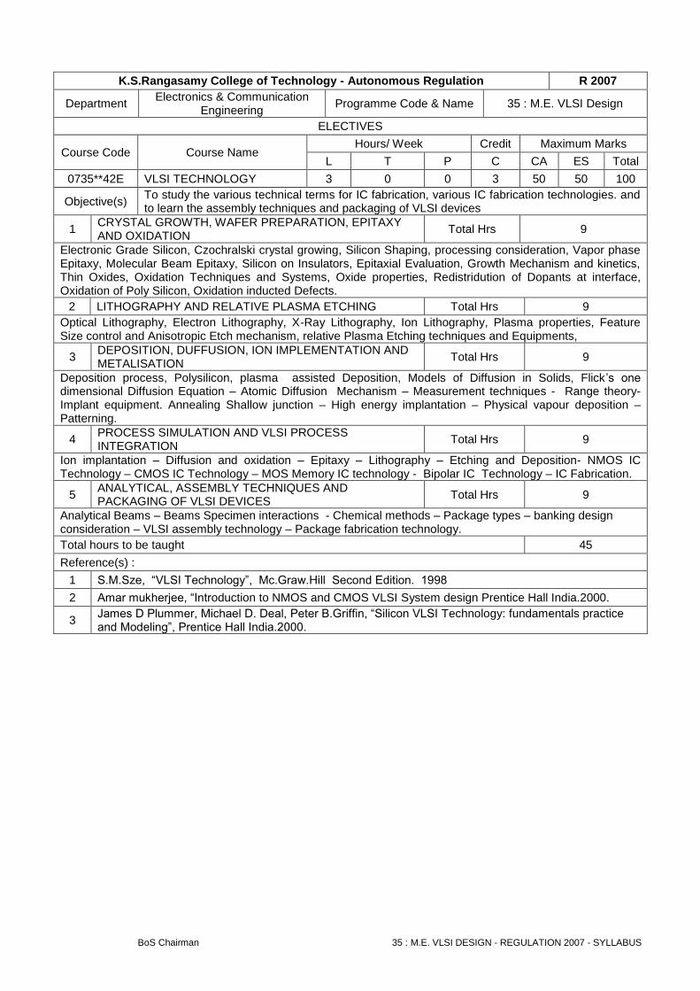
0735**42E VLSI TECHNOLOGY 3 0 0 3 50 50 100
Objective(s) To study the various technical terms for IC fabrication, various IC fabrication technologies. and to learn the assembly techniques and packaging of VLSI devices
1 CRYSTAL GROWTH, WAFER PREPARATION, EPITAXY AND OXIDATION
Total Hrs 9
Electronic Grade Silicon, Czochralski crystal growing, Silicon Shaping, processing consideration, Vapor phase Epitaxy, Molecular Beam Epitaxy, Silicon on Insulators, Epitaxial Evaluation, Growth Mechanism and kinetics, Thin Oxides, Oxidation Techniques and Systems, Oxide properties, Redistridution of Dopants at interface, Oxidation of Poly Silicon, Oxidation inducted Defects.
2 LITHOGRAPHY AND RELATIVE PLASMA ETCHING Total Hrs 9
Optical Lithography, Electron Lithography, X-Ray Lithography, Ion Lithography, Plasma properties, Feature Size control and Anisotropic Etch mechanism, relative Plasma Etching techniques and Equipments,
3 DEPOSITION, DUFFUSION, ION IMPLEMENTATION AND METALISATION
Total Hrs 9
Deposition process, Polysilicon, plasma assisted Deposition, Models of Diffusion in Solids, Flick ‘s one dimensional Diffusion Equation – Atomic Diffusion Mechanism – Measurement techniques - Range theory- Implant equipment. Annealing Shallow junction – High energy implantation – Physical vapour deposition – Patterning.
4 PROCESS SIMULATION AND VLSI PROCESS INTEGRATION
Total Hrs 9
Ion implantation – Diffusion and oxidation – Epitaxy – Lithography – Etching and Deposition- NMOS IC Technology – CMOS IC Technology – MOS Memory IC technology - Bipolar IC Technology – IC Fabrication.
5 ANALYTICAL, ASSEMBLY TECHNIQUES AND PACKAGING OF VLSI DEVICES
Total Hrs 9
Analytical Beams – Beams Specimen interactions - Chemical methods – Package types – banking design consideration – VLSI assembly technology – Package fabrication technology.
Total hours to be taught 45
Reference(s) :
1 S.M.Sze, ―VLSI Technology‖, Mc.Graw.Hill Second Edition. 1998
2 Amar mukherjee, ―Introduction to NMOS and CMOS VLSI System design Prentice Hall India.2000.
3 James D Plummer, Michael D. Deal, Peter B.Griffin, ―Silicon VLSI Technology: fundamentals practice and Modeling‖, Prentice Hall India.2000.
BoS Chairman 35 : M.E. VLSI DESIGN - REGULATION 2007 - SYLLABUS
K.S.Rangasamy College of Technology - Autonomous Regulation R 2007
Department Electronics & Communication Engineering Programme Code &
Name 34 : M.E. APPLIED
ELECTRONICS
ELECTIVES
Course Code Course Name Hours/ Week Credit Maximum Marks
L T P C CA ES Total
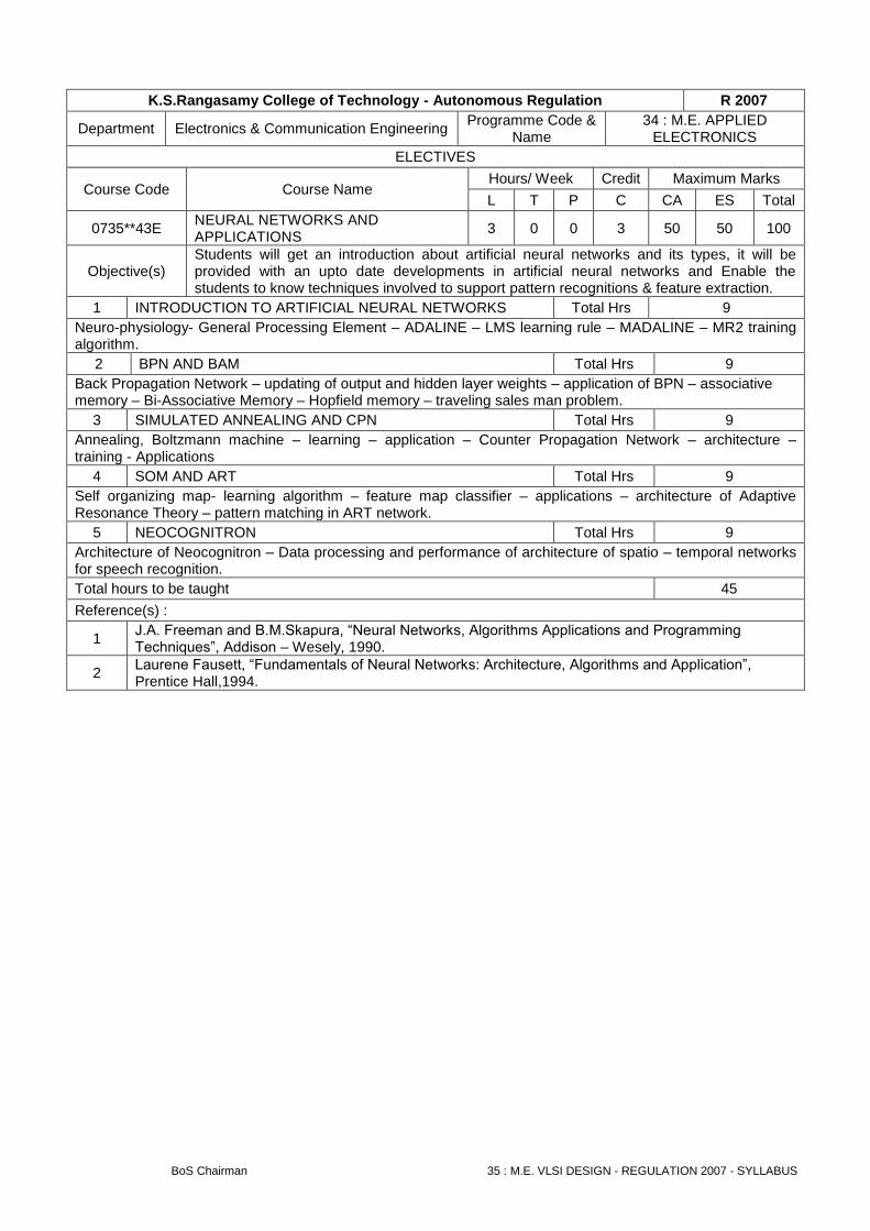
0735**43E NEURAL NETWORKS AND APPLICATIONS
3 0 0 3 50 50 100
Objective(s) Students will get an introduction about artificial neural networks and its types, it will be provided with an upto date developments in artificial neural networks and Enable the students to know techniques involved to support pattern recognitions & feature extraction.
1 INTRODUCTION TO ARTIFICIAL NEURAL NETWORKS Total Hrs 9
Neuro-physiology- General Processing Element – ADALINE – LMS learning rule – MADALINE – MR2 training algorithm.
2 BPN AND BAM Total Hrs 9
Back Propagation Network – updating of output and hidden layer weights – application of BPN – associative memory – Bi-Associative Memory – Hopfield memory – traveling sales man problem.
3 SIMULATED ANNEALING AND CPN Total Hrs 9
Annealing, Boltzmann machine – learning – application – Counter Propagation Network – architecture – training - Applications
4 SOM AND ART Total Hrs 9
Self organizing map- learning algorithm – feature map classifier – applications – architecture of Adaptive Resonance Theory – pattern matching in ART network.
5 NEOCOGNITRON Total Hrs 9
Architecture of Neocognitron – Data processing and performance of architecture of spatio – temporal networks for speech recognition.
Total hours to be taught 45
Reference(s) :
1 J.A. Freeman and B.M.Skapura, ―Neural Networks, Algorithms Applications and Programming Techniques‖, Addison – Wesely, 1990.
2 Laurene Fausett, ―Fundamentals of Neural Networks: Architecture, Algorithms and Application‖, Prentice Hall,1994.

BoS Chairman 35 : M.E. VLSI DESIGN - REGULATION 2007 - SYLLABUS
K.S.Rangasamy College of Technology - Autonomous Regulation R 2007
Department Electronics & Communication Engineering Programme Code &
Name 35 : M.E. VLSI DESIGN
ELECTIVES
Course Code Course Name Hours/ Week Credit Maximum Marks
L T P C CA ES Total
0735**44E DESIGN OF SEMICONDUCTOR MEMORIES
3 0 0 3 50 50 100
Objective(s) To learn the technologies for designing semiconductor memories, methods of testing semiconductor memories and the techniques involved in packaging of memories
1 RANDOM ACCESS MEMORY TECHNOLOGIES Total Hrs 9
STATIC RANDOM ACCESS MEMORIES (SRAMs): SRAM Cell Structures-MOS SRAM Architecture-MOS SRAM Cell and Peripheral Circuit Operation-BipolarSRAM Technologies-Silicon On Insulator (SOl) Technology-Advanced SRAM Architectures and Technologies-Application Specific SRAMs. DYNAMIC RANDOM ACCESS MEMORIES (DRAMs): DRAM Technology Development-CMOS DRAMs-DRAMs Cell Theory and Advanced Cell Strucutures-BiCMOS,DRAMs-Soft Error Failures in DRAMs-Advanced DRAM Designs and Architecture-Application Specific DRAMs.
2 NONVOLATILE MEMORIES Total Hrs 9
Masked Read-Only Memories (ROMs)-High Density ROMs-Programmable Read-Only Memories (PROMs)-BipolarPROMs-CMOS PROMs-Erasable (UV) - Programmable Road-Only Memories (EPROMs)-Floating-GateEPROM Cell-One-Time Programmable (OTP) Eproms-Electrically Erasable PROMs (EEPROMs)-EEPROM Technology And Arcitecture-Nonvolatile SRAM-Flash Memories (EPROMs or EEPROM)-AdvancedFlash Memory Architecture.
3 MEMORY FAULT MODELING, TESTING, AND MEMORY DESIGN FOR TESTABILITY AND FAULT TOLERANCE
Total Hrs 9
RAM Fault Modeling, Electrical Testing, Peusdo Random Testing-Megabit DRAM Testing-Nonvolatile Memory Modeling and Testing-IDDQ Fault Modeling and Testing-Application Specific Memory Testing
4 SEMICONDUCTOR MEMORY RELIABILITY AND RADIATION EFFECTS
Total Hrs 9
General Reliability Issues-RAM Failure Modes and Mechanism-Nonvolatile Memory Reliability-Reliability Modeling and Failure Rate Prediction-Design for Reliability-Reliability Test Structures-Reliability Screening andQualification. RAM Fault Modeling, Electrical Testing, Peusdo Random Testing-Megabit DRAM Testing-Nonvolatile Memory Modeling and Testing-IDDQ Fault Modeling and Testing-Application Specific Memory Testing.
5 PACKAGING TECHNOLOGIES Total Hrs 9
Radiation Effects-Single Event Phenomenon (SEP)-Radiation Hardening Techniques-Radiation Hardening Process and Design Issues-Radiation Hardened Memory Characteristics-Radiation Hardness Assurance and Testing - Radiation Dosimetry-Water Level Radiation Testing and Test Structures. Ferroelectric Random Access Memories (FRAMs)-Gallium Arsenide (GaAs) FRAMs-Analog Memories-Magnetoresistive Random Access Memories (MRAMs)-Experimental Memory Devices. Memory Hybrids and MCMs (2D)-Memory Stacks and MCMs (3D)-Memory MCM Testing and Reliability Issues-Memory Cards-High Density Memory Packaging Future Directions
Total hours to be taught 45
Reference(s) :
1 Ashok K. Sharma, ―Semiconductor Memories: Technology, Testing, and Reliability‖, Wiley-IEEE Press, 2002.
2 Ashok K. Sharma , ―Semiconductor Memories‖, Two-Volume Set, Wiley-IEEE Press, 2003.
3 Ashok K. Sharma, ―Semiconductor Memories: Technology, Testing, and Reliability‖, Prentice Hall of India, 1997.
BoS Chairman 35 : M.E. VLSI DESIGN - REGULATION 2007 - SYLLABUS
K.S.Rangasamy College of Technology - Autonomous Regulation R 2007
Department Electronics & Communication
Engineering Programme Code & Name 35 : M.E. VLSI Design
ELECTIVES
Course Code Course Name Hours/ Week Credit Maximum Marks
L T P C CA ES Total
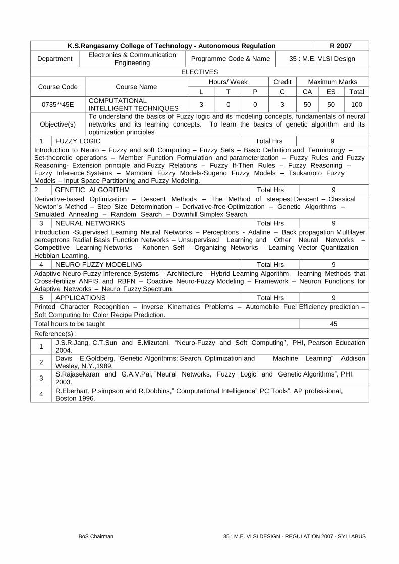
0735**45E COMPUTATIONAL INTELLIGENT TECHNIQUES
3 0 0 3 50 50 100
Objective(s) To understand the basics of Fuzzy logic and its modeling concepts, fundamentals of neural networks and its learning concepts. To learn the basics of genetic algorithm and its optimization principles
1 FUZZY LOGIC Total Hrs 9
Introduction to Neuro – Fuzzy and soft Computing – Fuzzy Sets – Basic Definition and Terminology – Set-theoretic operations – Member Function Formulation and parameterization – Fuzzy Rules and Fuzzy Reasoning- Extension principle and Fuzzy Relations – Fuzzy If-Then Rules – Fuzzy Reasoning – Fuzzy Inference Systems – Mamdani Fuzzy Models-Sugeno Fuzzy Models – Tsukamoto Fuzzy Models – Input Space Partitioning and Fuzzy Modeling.
2 GENETIC ALGORITHM Total Hrs 9
Derivative-based Optimization – Descent Methods – The Method of steepest Descent – Classical Newton‘s Method – Step Size Determination – Derivative-free Optimization – Genetic Algorithms – Simulated Annealing – Random Search – Downhill Simplex Search.
3 NEURAL NETWORKS Total Hrs 9
Introduction -Supervised Learning Neural Networks – Perceptrons - Adaline – Back propagation Multilayer perceptrons Radial Basis Function Networks – Unsupervised Learning and Other Neural Networks – Competitive Learning Networks – Kohonen Self – Organizing Networks – Learning Vector Quantization – Hebbian Learning.
4 NEURO FUZZY MODELING Total Hrs 9
Adaptive Neuro-Fuzzy Inference Systems – Architecture – Hybrid Learning Algorithm – learning Methods that Cross-fertilize ANFIS and RBFN – Coactive Neuro-Fuzzy Modeling – Framework – Neuron Functions for Adaptive Networks – Neuro Fuzzy Spectrum.
5 APPLICATIONS Total Hrs 9
Printed Character Recognition – Inverse Kinematics Problems – Automobile Fuel Efficiency prediction – Soft Computing for Color Recipe Prediction.
Total hours to be taught 45
Reference(s) :
1 J.S.R.Jang, C.T.Sun and E.Mizutani, ―Neuro-Fuzzy and Soft Computing‖, PHI, Pearson Education 2004.
2 Davis E.Goldberg, ‖Genetic Algorithms: Search, Optimization and Machine Learning‖ Addison Wesley, N.Y.,1989.
3 S.Rajasekaran and G.A.V.Pai, ‖Neural Networks, Fuzzy Logic and Genetic Algorithms‖, PHI, 2003.
4 R.Eberhart, P.simpson and R.Dobbins,‖ Computational Intelligence‖ PC Tools‖, AP professional, Boston 1996.

BoS Chairman 35 : M.E. VLSI DESIGN - REGULATION 2007 - SYLLABUS
K.S.Rangasamy College of Technology - Autonomous Regulation R 2007
Department Electronics & Communication Engineering Programme Code &
Name 35 : M.E. VLSI Design
ELECTIVES
Course Code Course Name Hours/ Week Credit Maximum Marks
L T P C CA ES Total
0735**46E ADVANCED MICROPROCESSORS AND MICROCONTROLLERS
3 0 0 3 50 50 100
Objective(s) If explain the architecture and addressing modes of 8086, MOTOROLA 68000 microprocessor, and also it explain the peripheral interface.
1 MICROPROCESSOR ARCHITECTURE Total Hrs 9
Instruction set – Data formats – Instruction formats – Addressing modes – Memory hierarchy – register file – Cache – Virtual memory and paging – Segmentation – Pipelining – The instruction pipeline – pipeline hazards – Instruction level parallelism – reduced instruction set – Computer principles – RISC versus CISC – RISC properties – RISC evaluation – On-chip register files versus cache evaluation.
2 HIGH PERFORMANCE CISC ARCHITECTURE – PENTIUM Total Hrs 9
The software model – functional description – CPU pin descriptions – RISC concepts – bus operations – Super scalar architecture – pipe lining – Branch prediction – The instruction and caches – Floating point unit –protected mode operation – Segmentation – paging – Protection – multitasking – Exception and interrupts – Input /Output – Virtual 8086 model – Interrupt processing -Instruction types – Addressing modes – Processor flags – Instruction set -programming the Pentium processor.
3 HIGH PERFORMANCE RISC ARCHITECTURE :ARM Total Hrs 9
The ARM architecture – ARM assembly language program – ARM organization and implementation – The ARM instruction set - The thumb instruction set – ARM CPU cores.
4 MOTOROLA 68HC11 MICROCONTROLLERS Total Hrs 9
Instructions and addressing modes – operating modes – Hardware reset – Interrupt system – Parallel I/O ports – Flags – Real time clock – Programmable timer – pulse accumulator – serial communication interface – A/D converter – hardware expansion – Assembly language Programming.
5 PIC MICRO CONTROLLER Total Hrs 9
CPU architecture – Instruction set - Interrupts – Timers – I/O port expansion –I2C bus for peripheral chip access
– A/D converter – UART.
Total hours to be taught 45
Reference(s) :
1 Daniel Tabak , ‗‘ Advanced Microprocessors‖ McGraw Hill.Inc., 1995.
2 James L. Antonakos , ― The Pentium Microprocessor ‗‘ Pearson Education , 1997.
3 Steve Furber , ‗‘ ARM System –On –Chip architecture ―Addison Wesley , 2000.
4 John .B.Peatman , ― Design with PIC Microcontroller , Prentice hall, 1997.

BoS Chairman 35 : M.E. VLSI DESIGN - REGULATION 2007 - SYLLABUS
K.S.Rangasamy College of Technology - Autonomous Regulation R 2007
Department Electronics & Communication
Engineering Programme Code &
Name 35 : M.E. VLSI Design
ELECTIVES
Course Code Course Name Hours/ Week Credit Maximum Marks
L T P C CA ES Total
0735**47E LOW POWER VLSI DESIGN 3 0 0 3 50 50 100
Objective(s) To emphasize the optimization and trade – off techniques that involve power dissipation, and to highlight the basic principles, methodologies and techniques that are common to CMOS digital design.
1 POWER DISSIPATION IN CMOS Total Hrs 9
Hierarchy of limits of power – Sources of power consumption – Physics of power dissipation in CMOS FET devices- Basic principle of low power design.
2 POWER OPTIMIZATION Total Hrs 9
Logical level power optimization – Circuit level low power design – Circuit techniques for reducing power consumption in adders and multipliers.
3 DESIGN OF LOW POWER CMOS CIRCUITS Total Hrs 9
Computer Arithmetic techniques for low power systems – Reducing power consumption in memories – Low power clock, Interconnect and layout design – Advanced techniques – Special techniques
4 POWER ESTIMATION Total Hrs 9
Power estimation techniques – Logic level power estimation – Simulation power analysis – Probabilistic power analysis.
5 SYNTHESIS AND SOFTWARE DESIGN FOR LOW POWER Total Hrs 9
Synthesis for low power –Behavioral level transforms- Software design for low power.
Total hours to be taught 45
Reference(s) :
1 K.Roy and S.C. Prasad , LOW POWER CMOS VLSI circuit design, Wiley,2000.
2 Dimitrios Soudris, Chirstian Pignet, Costas Goutis, DESIGNING CMOS CIRCUITS FOR LOW POWER, Kluwer,2002.
3 B. Kuo and J.H Lou, Low voltage CMOS VLSI Circuits, Wiley 1999.
4 John .B.Peatman , ― Design with PIC Microcontroller , Prentice hall, 1997.
5 James B. Kuo, Shin – chia Lin, Low voltage SOI CMOS VLSI Devices and Circuits. John Wiley and sons, inc 2001.

BoS Chairman 35 : M.E. VLSI DESIGN - REGULATION 2007 - SYLLABUS
K.S.Rangasamy College of Technology - Autonomous Regulation R 2007
Department Electronics & Communication
Engineering Programme Code &
Name 35 : M.E. VLSI Design
ELECTIVES
Course Code Course Name Hours/ Week Credit Maximum Marks
L T P C CA ES Total
0735**48E ANALOG VLSI DESIGN 3 0 0 3 50 50 100
Objective(s)
Introduction to Analog VLSI and Basic CMOS and BiCMOS Circuit Techniques, Concepts of Continuous-Time Signal Processing- Low-Voltage Signal Processing and Current-Mode Signal Processing. Neural Information Processing and Analog VLSI Interconnects , design of Sampled Data Analog Filters and Over sampled A/D Converters
1 BASIC CMOS CIRCUIT TECHNIQUES, CONTINUOUS TIME AND LOW-VOLTAGE SIGNALPROCESSING
Total Hrs 9
Mixed-Signal VLSI Chips-Basic CMOS Circuits-Basic Gain Stage-Gain Boosting Techniques-Super MOSTransistor- Primitive Analog Cells-Linear Voltage-Current Converters-MOS Multipliers and Resistors-CMOS,Bipolar and Low-Voltage BiCMOS Op-Amp Design-Instrumentation Amplifier Design-Low Voltage Filters.
2 BASIC BICMOS CIRCUIT TECHNIQUES, CURRENT -MODE SIGNAL PROCESSING AND NEURAL INFORMATION PROCESSING
Total Hrs 9
Continuous-Time Signal Processing-Sampled-Data Signal Processing-Switched-Current Data Converters-Practical Considerations in SI Circuits Biologically-Inspired Neural Networks - Floating - Gate, Low-Power Neural Networks-CMOS Technology and Models-Design Methodology-Networks-Contrast Sensitive Silicon Retina.
3 SAMPLED-DATA ANALOG FILTERS, OVER SAMPLED A/D CONVERTERS AND ANALOG INTEGRATED SENSORS
Total Hrs 9
First-order and Second SC Circuits-Bilinear Transformation - Cascade Design-Switched-Capacitor Ladder Filter-Synthesis of Switched-Current Filter- Nyquist rate A/D Converters-Modulators for Over sampled A/D Conversion-First and Second Order and Multibit Sigma-Delta Modulators-Interpolative Modulators –Cascaded Architecture-Decimation Filters-mechanical, Thermal, Humidity and Magnetic Sensors-Sensor Interfaces.
4 DESIGN FOR TESTABILITY AND ANALOG VLSI INTERCONNECTS
Total Hrs 9
Fault modelling and Simulation - Testability-Analysis Technique-Ad Hoc Methods and General Guidelines-Scan Techniques-Boundary Scan-Built-in Self Test-Analog Test Buses-Design for Electron -Beam Testablity-Physics of Interconnects in VLSI-Scaling of Interconnects-A Model for Estimating Wiring Density-A Configurable Architecture for Prototyping Analog Circuits.
5 STATISTICAL MODELING AND SIMULATION, ANALOG COMPUTER-AIDED DESIGN AND ANALOG AND MIXED ANALOG-DIGITAL LAYOUT
Total Hrs 9
Review of Statistical Concepts - Statistical Device Modeling- Statistical Circuit Simulation-Automation Analog Circuit Design-automatic Analog Layout-CMOS Transistor Layout-Resistor Layout-Capacitor Layout-Analog Cell Layout-Mixed Analog -Digital Layout
Total hours to be taught 45
Reference(s) :
1 Mohammed Ismail, Terri Fiez, ―Analog VLSI signal and Information Processing ", McGraw-Hill International Editons, 1994.
2 Malcom R.Haskard, Lan C.May, ―Analog VLSI Design - NMOS and CMOS ", Prentice Hall, 1998.
3 Randall L Geiger, Phillip E. Allen, " Noel K.Strader, VLSI Design Techniques for Analog and Digital Circuits ", Mc Graw Hill International Company, 1990

BoS Chairman 35 : M.E. VLSI DESIGN - REGULATION 2007 - SYLLABUS
K.S.Rangasamy College of Technology - Autonomous Regulation R 2007
Department Electronics & Communication
Engineering Programme Code &
Name 35 : M.E. VLSI Design
ELECTIVES
Course Code Course Name Hours/ Week Credit Maximum Marks
L T P C CA ES Total
0735**49E ASIC DESIGN 3 0 0 3 50 50 100
Objective(s) To Know about the hardware and software which are involved in an application specific integrated circuits. And to know how to design an application specific integrated circuits for a specific application.
1 INTRODUCTION TO ASICS, CMOS LOGIC AND ASIC LIBRARY DESIGN
Total Hrs 9
Types of ASICs - Design flow - CMOS transistors CMOS Design rules - Combinational Logic Cell – Sequential logic cell - Data path logic cell - Transistors as Resistors - Transistor Parasitic Capacitance- Logical effort –Library cell design - Library architecture.
2 PROGRAMMABLE ASICS, PROGRAMMABLE ASIC LOGIC CELLS AND PROGRAMMABLE ASIC I/O CELLS
Total Hrs 9
Anti fuse - static RAM - EPROM and EEPROM technology - PREP benchmarks - Actel ACT - Xilinx LCA –Altera FLEX - Altera MAX DC & AC inputs and outputs - Clock & Power inputs - Xilinx I/O blocks.
3 PROGRAMMABLE ASIC INTERCONNECT, PROGRAMMABLE ASIC DESIGN SOFTWARE AND LOW LEVEL DESIGN ENTRY
Total Hrs 9
Actel ACT -Xilinx LCA - Xilinx EPLD - Altera MAX 5000 and 7000 - Altera MAX 9000 - Altera FLEX –Design systems - Logic Synthesis - Half gate ASIC -Schematic entry - Low level design language - PLA tools -EDIF- CFI design representation.
4 LOGIC SYNTHESIS, SIMULATION AND TESTING Total Hrs 9
Verilog and logic synthesis -VHDL and logic synthesis - types of simulation -boundary scan test - fault simulation - automatic test pattern generation.
5 ASIC CONSTRUCTION, FLOOR PLANNING, PLACEMENT AND ROUTING
Total Hrs 9
System partition - FPGA partitioning - partitioning methods - floor planning - placement - physical design flow –global routing - detailed routing - special routing - circuit extraction - DRC.
Total hours to be taught 45
Reference(s) :
1 M.J.S .Smith, "Application Specific Integrated Circuits, Addison -Wesley Longman Inc., 1997.
2 Farzad Nekoogar and Faranak Nekoogar, From ASICs to SOCs: A Practical Approach, Prentice Hall PTR, 2003
3 Wayne Wolf, FPGA-Based System Design, Prentice Hall PTR, 2004

BoS Chairman 35 : M.E. VLSI DESIGN - REGULATION 2007 - SYLLABUS
K.S.Rangasamy College of Technology - Autonomous Regulation R 2007
Department Electronics & Communication
Engineering Programme Code &
Name 35 : M.E. VLSI Design
ELECTIVES
Course Code Course Name Hours/ Week Credit Maximum Marks
L T P C CA ES Total
0735**50E GENETIC ALGORITHMS AND THEIR APPLICATIONS
3 0 0 3 50 50 100
Objective(s) Introduction to GA Technology, Placement Technology, Routing Technology and Test Generation Patterns
1 Total Hrs 9
Introduction, A Technology-Steady State Algorithm-Fitness Scaling-Inversion
2 Total Hrs 9
GA for VLSI Design, Layout and Test automation- partitioning-automatic placement, routing technology, Mapping for FPGA- Automatic test generation- Partitioning algorithm Taxonomy-Multiway Partitioning
3 Total Hrs 9
Hybrid genetic – genetic encoding-local improvement-WDFR-Comparison of Cas- Standard cell placement-GASP algorithm-unified algorithm.
4 Total Hrs 9
Global routing-FPGA technology mapping-circuit generation-test generation in a GA frame work-test generation procedures.
5 Total Hrs 9
Power estimation-application of GA-Standard cell placement-GA for ATG-problem encoding- fitness function-GA vs Conventional algorithm.
Total hours to be taught 45
Reference(s) :
1 Pinaki Mazumder, E.MRudnick, ‖Genetic Algorithm for VLSI Design, Layout and test Automation‖, Prentice Hall,1998.
2 Randy L. Haupt, Sue Ellen Haupt, ―Practical Genetic Algorithms‖ Wiley – Interscience,1977.
3 Ricardo Sal Zebulum, Macro Aurelio Pacheco, Marley Maria B.R. Vellasco, Marley Maria Bernard Vellasco ―Evolution Electronics: Automatic Design of electronic Circuits and Systems Genetic Algorithms‖, CRC press, 1
st Edition Dec 2001.
4 John R.Koza, Forrest H.Bennett III, David Andre , Morgan Kufmann, ―Genetic Programming Automatic programming and Automatic Circuit Synthesis‖, 1
st Edition , May 1999

BoS Chairman 35 : M.E. VLSI DESIGN - REGULATION 2007 - SYLLABUS
K.S.Rangasamy College of Technology - Autonomous Regulation R 2007
Department Electronics & Communication
Engineering Programme Code &
Name 35 : M.E. VLSI Design
ELECTIVES
Course Code Course Name Hours/ Week Credit Maximum Marks
L T P C CA ES Total
0735**51E ELECTROMAGNETIC INTERFERENCE AND COMPATIBILITY IN SYSTEM DESIGN
3 0 0 3 50 50 100
Objective(s) To study about EMI Environment, EMI Coupling Principles , EMI Specification ,Standards and Limits and EMI Measurements and Control
1 EMI ENVIRONMENT Total Hrs 9
EMI/EMC concepts and definitions, Sources of EMI, conducted and radiated EMI, Transient EMI, Time domain Vs Frequency domain EMI, Units of measurement parameters, Emission and immunity concepts, ESD.
2 EMI COUPLING PRINCIPLES Total Hrs 9
Conducted, Radiated and Transient Coupling, Common Impedance Ground Coupling, Radiated Common Mode and Ground Loop Coupling, Radiated Differential Mode Coupling, Near Field Cable to Cable Coupling, Power Mains and Power Supply coupling.
3 EMI/EMC STANDARDS AND MEASUREMENTS Total Hrs 9
Civilian standards - FCC,CISPR,IEC, EN, Military standards - MIL STD 461D/462, EMI Test Instruments /Systems, EMI Shielded Chamber, Open Area Test Site, TEM Cell, Sensors/Injectors/Couplers, Test beds for ESD and EFT, Military Test Method and Procedures (462).
4 EMI CONTROL TECHNIQUES Total Hrs 9
Shielding, Filtering, Grounding, Bonding, Isolation Transformer, Transient Suppressors, Cable Routing, Signal Control, Component Selection and Mounting.
5 EMC DESIGN OF PCBs Total Hrs 9
PCB Traces Cross Talk, Impedance Control, Power Distribution Decoupling, Zoning, Motherboard Designs and Propagation Delay Performance Models
Total hours to be taught 45
Reference(s) :
1 Henry W.Ott, "Noise Reduction Techniques in Electronic Systems", John Wiley and Sons, NewYork. 1988.
2 C.R.Paul, ―Introduction to Electromagnetic Compatibility‖ , John Wiley and Sons, Inc, 1992
3 V.P.Kodali, "Engineering EMC Principles, Measurements and Technologies", IEEE Press, 1996.

BoS Chairman 35 : M.E. VLSI DESIGN - REGULATION 2007 - SYLLABUS
K.S.Rangasamy College of Technology - Autonomous Regulation R 2007
Department Electronics & Communication
Engineering Programme Code &
Name 35 : M.E. VLSI Design
ELECTIVES
Course Code Course Name
Hours/ Week Credit Maximum Marks
L T P C CA ES Tota
l
0735**52E SPEECH AND AUDIO SIGNAL PROCESSING
3 0 0 3 50 50 100
Objective(s) Introduction to Analog VLSI and Basic CMOS and BiCMOS Circuit Techniques, Concepts of Continuous-Time Signal Processing- Low-Voltage Signal Processing and Current-Mode Signal Processing and Neural Information Processing and Analog VLSI Interconnects.
1 MECHANICS OF SPEECH Total Hrs 9
Speech production mechanism – Nature of Speech signal – Discrete time modelling of Speech production – Representation of Speech signals – Classification of Speech sounds – Phones – Phonemes – Phonetic and Phonemic alphabets – Articulatory features. Music production – Auditory perception – Anatomical pathways from the ear to the perception of sound – Peripheral auditory system – Psycho acoustics.
2 TIME DOMAIN METHODS FOR SPEECH PROCESSING Total Hrs 9
Time domain parameters of Speech signal – Methods for extracting the parameters Energy, Average Magnitude – Zero crossing Rate – Silence Discrimination using ZCR and energy – Short Time Auto Correlation Function – Pitch period estimation using Auto Correlation Function.
3 FREQUENCY DOMAIN METHOD FOR SPEECH PROCESSING
Total Hrs 9
Short Time Fourier analysis – Filter bank analysis – Formant extraction – Pitch Extraction – Analysis by Synthesis- Analysis synthesis systems- Phase vocoder—Channel Vocoder. HOMOMORPHIC SPEECH ANALYSIS: Cepstral analysis of Speech – Formant and Pitch Estimation – Homomorphic Vocoders.
4 LINEAR PREDICTIVE ANALYSIS OF SPEECH Total Hrs 9
Formulation of Linear Prediction problem in Time Domain – Basic Principle – Auto correlation method – Covariance method – Solution of LPC equations – Cholesky method – Durbin‘s Recursive algorithm – lattice formation and solutions – Comparison of different methods – Application of LPC parameters – Pitch detection using LPC parameters – Formant analysis – VELP – CELP.
5 APPLICATION OF SPEECH & AUDIO SIGNAL PROCESSING
Total Hrs 9
Algorithms: Spectral Estimation, dynamic time warping, hidden Markov model – Music analysis – Pitch Detection – Feature analysis for recognition – Music synthesis – Automatic Speech Recognition – Feature Extraction for ASR – Deterministic sequence recognition – Statistical Sequence recognition – ASR systems – Speaker identification and verification – Voice response system – Speech Synthesis: Text to speech, voice over IP.
Total hours to be taught 45
Reference(s) :
1 Ben Gold and Nelson Morgan, Speech and Audio Signal Processing, John Wiley and Sons Inc. , Singapore, 2004.
2 L.R.Rabiner and R.W.Schaffer – Digital Processing of Speech signals – Prentice Hall -1978.
3 Quatieri – Discrete-time Speech Signal Processing – Prentice Hall – 2001.

BoS Chairman 35 : M.E. VLSI DESIGN - REGULATION 2007 - SYLLABUS
K.S.Rangasamy College of Technology - Autonomous Regulation R 2007
Department Electronics & Communication
Engineering Programme Code &
Name 35 : M.E. VLSI Design
ELECTIVES
Course Code Course Name Hours/ Week Credit Maximum Marks
L T P C CA ES Total
0735**53E RELIABILITY ENGINEERING 3 0 0 3 50 50 100
Objective(s) Reliability Fundamentals, basics of system reliability and device reliability. Reliability techniques maintainability and availability concepts
1 PROBABILITY PLOTTING AND LOAD-STRENGTH INTERFERENCE
Total Hrs 9
Statistical distribution , statistical confidence and hypothesis testing ,probability plotting techniques – Weibull, extreme value ,hazard, binomial data; Analysis of load – strength interference , Safety margin and loading roughness on reliability.
2 RELIABILITY PREDICTION, MODELLING AND DESIGN Total Hrs 9
Statistical design of experiments and analysis of variance Taguchi method, Reliability prediction, Reliability modeling, Block diagram and Fault tree Analysis ,petric Nets, State space Analysis, Monte carlo simulation, Design analysis methods – quality function deployment, load strength analysis, failure modes, effects and criticality analysis.
3 ELECTRONICS AND SOFTWARE SYSTEMS RELIABILITY Total Hrs 9
Reliability of electronic components, component types and failure mechanisms, Electronic system reliability prediction, Reliability in electronic system design; software errors, software structure and modularity, fault tolerance, software reliability, prediction and measurement, hardware/software interfaces
4 RELIABILITY TESTING AND ANALYSIS Total Hrs 9
Test environments, testing for reliability and durability, failure reporting, Pareto analysis, Accelerated test data analysis, CUSUM charts, Exploratory data analysis and proportional hazards modeling, reliability demonstration, reliability growth monitoring.
5 MANUFACTURE AND RELIABILITY MAQNAGEMENT Total Hrs 9
Control of production variability, Acceptance sampling, Quality control and stress screening, Production failure reporting; preventive maintenance strategy, Maintenance schedules, Design for maintainability, Integrated reliability programmes, reliability and costs, standard for reliability, quality and safety, specifying reliability, organization for reliability.
Total hours to be taught 45
Reference(s) :
1 Patrick D.T. O‘Connor, David Newton and Richard Bromley, Practical Reliability Engineering, Fourth edition, John Wiley & Sons, 2002
2 David J. Klinger, Yoshinao Nakada and Maria A. Menendez, Von Nostrand Reinhold, New York, "AT & T Reliability Manual", 5th Edition, 1998.
3 Gregg K. Hobbs, "Accelerated Reliability Engineering - HALT and HASS", John Wiley & Sons, New York, 2000.

BoS Chairman 35 : M.E. VLSI DESIGN - REGULATION 2007 - SYLLABUS
K.S.Rangasamy College of Technology - Autonomous Regulation R 2007
Department Electronics & Communication
Engineering Programme Code &
Name 35 : M.E. VLSI Design
ELECTIVES
Course Code Course Name Hours/ Week Credit Maximum Marks
L T P C CA ES Total
0735**54E DSP PROCESSOR ARCHITECTURE AND PROGRAMMING
3 0 0 3 50 50 100
Objective(s) Introduction to DSP Processors, Architecture of TMS320C5X and TMS320C3X Processor. and introduction of DSP family processors.
1 FUNDAMENTALS OF PROGRAMMABLE DSPs Total Hrs 9
Multiplier and Multiplier accumulator – Modified Bus Structures and Memory access in P-DSPs – Multiple access memory – Multi-port memory – VLIW architecture- Pipelining – Special Addressing modes in P-DSPs – On chip Peripherals.
2 TMS320C5X PROCESSOR Total Hrs 9
Architecture – Assembly language syntax - Addressing modes – Assembly language Instructions - Pipeline structure, Operation – Block Diagram of DSP starter kit – Application Programs for processing real time signals.
3 TMS320C3X PROCESSOR Total Hrs 9
Architecture – Data formats - Addressing modes – Groups of addressing modes- Instruction sets - Operation – Block Diagram of DSP starter kit – Application Programs for processing real time signals – Generating and finding the sum of series, Convolution of two sequences, Filter design
4 ADSP PROCESSORS Total Hrs 9
Architecture of ADSP-21XX and ADSP-210XX series of DSP processors- Addressing modes and assembly language instructions – Application programs –Filter design, FFT calculation.
5 ADVANCED PROCESSORS Total Hrs 9
Architecture of TMS320C54X: Pipe line operation, Code Composer studio - Architecture of TMS320C6X - Architecture of Motorola DSP563XX – Comparison of the features of DSP family processors.
Total hours to be taught 45
Reference(s) :
1 B.Venkataramani and M.Bhaskar, ―Digital Signal Processors – Architecture, Programming and Applications‖ – Tata McGraw – Hill Publishing Company Limited. New Delhi, 2003
2 User guides Texas Instrumentation, Analog Devices, Motorola.
BoS Chairman 35 : M.E. VLSI DESIGN - REGULATION 2007 - SYLLABUS
K.S.Rangasamy College of Technology - Autonomous Regulation R 2007
Department Electronics & Communication
Engineering Programme Code &
Name 35 : M.E. VLSI Design
ELECTIVES
Course Code Course Name Hours/ Week Credit Maximum Marks
L T P C CA ES Total
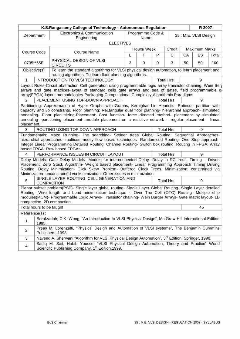
0735**55E PHYSICAL DESIGN OF VLSI CIRCUITS
3 0 0 3 50 50 100
Objective(s)
To learn the standard algorithms for VLSI physical design automation, to learn placement and routing algorithms. To learn floor planning algorithms.
1 INTRODUCTION TO VLSI TECHNOLOGY Total Hrs 9
Layout Rules-Circuit abstraction Cell generation using programmable logic array transistor chaining, Wein Berger arrays and gate matrices-layout of standard cells gate arrays and sea of gates, field programmable gate array(FPGA)-layout methodologies-Packaging-Computational Complexity-Algorithmic Paradigms
2 PLACEMENT USING TOP-DOWN APPROACH Total Hrs 9
Partitioning: Approximation of Hyper Graphs with Graphs, Kernighan-Lin Heuristic- Ratiocut- partition with capacity and i/o constrants. Floor planning: Rectangular dual floor planning- hierarchial approach- simulated annealing- Floor plan sizing-Placement: Cost function- force directed method- placement by simulated annealing- partitioning placement- module placement on a resistive network – regular placement- linear placement.
3 ROUTING USING TOP DOWN APPROACH Total Hrs 9
Fundamentals: Maze Running- line searching- Steiner trees Global Routing: Sequential Approaches- hierarchial approaches- multicommodity flow based techniques- Randomised Routing- One Step approach- Integer Linear Programming Detailed Routing: Channel Routing- Switch box routing. Routing in FPGA: Array based FPGA- Row based FPGAs
4 PERFORMANCE ISSUES IN CIRCUIT LAYOUT Total Hrs 9
Delay Models: Gate Delay Models- Models for interconnected Delay- Delay in RC trees. Timing – Driven Placement: Zero Stack Algorithm- Weight based placement- Linear Programming Approach Timing Driving Routing: Delay Minimization- Click Skew Problem- Buffered Clock Trees. Minimization: constrained via Minimization- unconstrained via Minimization- Other issues in minimization
5 SINGLE LAYER ROUTING, CELL GENERATION AND COMPACTION
Total Hrs 9
Planar subset problem(PSP)- Single layer global routing- Single Layer Global Routing- Single Layer detailed Routing- Wire length and bend minimization technique – Over The Cell (OTC) Routing- Multiple chip modules(MCM)- Programmable Logic Arrays- Transistor chaining- Wein Burger Arrays- Gate matrix layout- 1D compaction- 2D compaction.
Total hours to be taught 45
Reference(s) :
1 Sarafzadeh, C.K. Wong, ―An Introduction to VLSI Physical Design‖, Mc Graw Hill International Edition 1995.
2 Preas M. Lorenzatti, ―Physical Design and Automation of VLSI systems‖, The Benjamin Cummins Publishers, 1998.
3 Naveed A. Sherwani ―Algorithm for VLSI Physical Design Automation‖, 3rd
Edition, Springer, 1998.
4 Sadiq M. Sait, Habib Youssef ―VLSI Physical Design Automation, Theory and Practice‖ World Scientific Publishing Company, 1
st Edition,1999.

BoS Chairman 35 : M.E. VLSI DESIGN - REGULATION 2007 - SYLLABUS
K.S.Rangasamy College of Technology - Autonomous Regulation R 2007
Department Electronics & Communication
Engineering Programme Code &
Name 35 : M.E. VLSI Design
ELECTIVES
Course Code Course Name Hours/ Week Credit Maximum Marks
L T P C CA ES Total
0735**56E DIGITAL IMAGE PROCESSING 3 0 0 3 50 50 100
Objective(s) To study the image fundamentals and mathematical transforms necessary for image processing.
1 DIGITAL IMAGE FUNDAMENTALS Total Hrs 9
Fundamental steps in Digital Image processing – Components of an image processing system - - elements of visual perception – Image sensing and acquisition- image sampling and quantization.
2 IMAGE TRANSFORMS Total Hrs 9
Two dimensional orthogonal and unitary transforms - properties of unitary transforms - one dimensional DFT - - two dimensional DFT- DCT, Discrete sine, Walsh, Hadamard , Slant, Haar, KLT, SVD, Radom and wavelet transforms.
3 IMAGE ENHANCEMENT AND RESTORATION Total Hrs 9
Basic gray level transformations – Histogram equalization – Histogram matching -spatial filtering – smoothing spatial filters – sharpening spatial filters- model of the image degradation / Restoration process- mean filters – order – statistics filters- Adaptive filters – Inverse filtering – minimum mean square error filtering – constrained least squares filtering – Geometric mean filter – geometric transformations.
4 IMAGE SEGMENTATION AND RECOGNITION Total Hrs 9
Detection of Discontinuities – Edge linking and boundary detection – Region based segmentation – morphological operators: Dilation, erosion, opening and closing. Image recognition patterns and pattern classes. Recognition based on decision – theoretic methods.
5 IMAGE COMPRESSION Total Hrs 9
Fundamentals of Image compression - Image compression models – Error free Compression – Lossy Compression – Image compression standards
Total hours to be taught 45
Reference(s) :
1 Gonzalez Rafel C, Woods Richard E, "Digital Image Processing", second edition. Prentice Hall , 2006
2 Jain Anil K , "Fundamentals of Digital Image Processing-" , Prentice Hall of India, 2003

BoS Chairman 35 : M.E. VLSI DESIGN - REGULATION 2007 - SYLLABUS
K.S.Rangasamy College of Technology - Autonomous Regulation R 2007
Department Electronics & Communication
Engineering Programme Code &
Name 35 : M.E. VLSI Design
ELECTIVES
Course Code Course Name Hours/ Week Credit Maximum Marks
L T P C CA ES Total
0735**57E COMPUTER ARCHITECTURE AND PARALLEL PROCESSING
3 0 0 3 50 50 100
Objective(s) To understand the basic principles of parallel processing, gain the knowledge of various computer architecture. To learn the efficient algorithms of parallel computer
1 PRINCIPLES OF PARALLEL PROCESSING Total Hrs 9
Multiprocessors and Multicomputers – Multivector and SIMD Computers- PRAM and VLSI Models- Conditions of Parallelism- Program Partitioning and scheduling-program flow mechanisms- parallel processing applications- speed up performance law.
2 PROCESSOR AND MEMORY ORGANIZATION Total Hrs 9
Advanced processor technology – Superscalar and vector processors- Memory hierarchy technology- Virtual memory technology- Cache memory organization- Shared memory organization.
3 PIPELINE AND PARALLEL ARCHITECTURE Total Hrs 9
Linear pipeline processors- Non linear pipeline processors- Instruction pipeline design- Arithmetic design- Superscalar and super pipeline design- Multiprocessor system interconnects- Message passing mechanisms.
4 VECTOR, MULTITHREAD AND DATAFLOW ARCHITECTURE Total Hrs 9
Vector Processing principle- Multivector Multiprocessors- Compound Vector processing- Principles of multithreading-fine grain multicomputers- scalable and multithread architectures – Dataflow and hybrid architectures.
5 SOFTWARE AND PARALLEL PROCESSING Total Hrs 9
Parallel programming models- parallel languages and compilers- parallel programming environments- synchronization and multiprocessing modes- message passing program development- mapping programs onto multicomputers- multiprocessor UNIX design goals- MACH/OS kernel architecture- OSF/1 architecture and applications.
Total hours to be taught 45
Reference(s) :
1 Kai Hwang, Advanced Computer Architecture, TMH 2001.
2 William Stallings, Computer Organization and Architecture, McMillan Publishing Company, 1990.
3 M.J. Quinn, Designing efficient Algorithms for parallel computer, McGraw Hill International, 1994.