Embed Size (px)
Citation preview
KTa0.5Nb0.5O3 ferroelectric thin films: processing,
characterization and application to microwave agile
devices
Vincent Laur, Arnaud-Gides Moussavou, Anthony Rousseau, Paul Laurent,
Gerard Tanne, Valerie Bouquet, Maryline Guilloux-Viry, Fabrice Huret
To cite this version:
Vincent Laur, Arnaud-Gides Moussavou, Anthony Rousseau, Paul Laurent, Gerard Tanne, etal.. KTa0.5Nb0.5O3 ferroelectric thin films: processing, characterization and application tomicrowave agile devices. Resarch Program of Regional Interest DISCOTEC - BRETAGNECollaboration(s). 2008. <hal-00276991>
HAL Id: hal-00276991
https://hal.archives-ouvertes.fr/hal-00276991
Submitted on 5 May 2008
HAL is a multi-disciplinary open accessarchive for the deposit and dissemination of sci-entific research documents, whether they are pub-lished or not. The documents may come fromteaching and research institutions in France orabroad, or from public or private research centers.
L’archive ouverte pluridisciplinaire HAL, estdestinee au depot et a la diffusion de documentsscientifiques de niveau recherche, publies ou non,emanant des etablissements d’enseignement et derecherche francais ou etrangers, des laboratoirespublics ou prives.

1
Frequenz
59 (2005) 7-8
KTa0.5Nb0.5O3 ferroelectric thin films: processing, characterization and appli-cation to microwave agile devices By V. Laur, A. Moussavou, A. Rousseau, P. Laurent, G. Tanné, V. Bouquet, M. Guilloux-Viry, F. Huret
Abstract
This paper is aimed at demonstrating the high capabilities of KTa0.5Nb0.5O3 thin films for micro-
wave agility applications. Tunable capacitors, resonators and phase shifters were realized with KTN materials. Their high frequency measurements showed, in particular, the very high tuning factors of these films under quite low electric field.
Index Terms
Ferroelectrics, Interdigital Capacitors, Phase Shifters, Stub Resonators, Thin Films
1. Introduction
Nowadays, numerous agile devices are needed in the telecommu-nication area. Indeed, reconfigurable circuits are expected to enable the development of many emerging systems such as multi-standard terminals or active antennas and to make them accessible to the general public.
At the moment, the technologies used to realize agile devices are unable to face up to the drastic industrial requirements compatible with a large diffusion of these systems. For example, ferrite materi-als are used for the realization of active antennas dedicated to mili-tary applications, but the weight of such front-ends is incompatible with mobile applications. More recently, semi-conductor compo-nents have been used to replace ferrite materials, but the cost of the global systems is too high to attract a large number of customers.
Another way to realize agile devices is to use ferroelectric materi-als. Since the eighties, progressive improvements in the way of processing films have led to the availability of thin films with excel-lent properties in term of homogeneity, microstructure, permittivity, and even losses though at a lesser degree. Thin-films are very prom-ising for a global IC integration; moreover, the control voltages required for getting good tuning factors are also lowered. Their very short switching times let the possibility to realize real-time tunable applications. The electrical control can be easily integrated in mi-crowave circuits achieved, in particular, in planar technologies. Finally, their power consumption is quasi null. Nevertheless, in spite of the recent progresses achieved in film processing, their dielectric losses remain too high. The focus of the most recent studies is the reduction of losses by different methods such as dielectric doping, mixing ferroelectric compositions or increasing the film quality (oxygen vacancies, interdiffusions, ).
Till now, most of the microwave studies on ferroelectrics have dealt with Ba1-xSrxTiO3 materials, which proved to exhibit very good properties at microwave frequencies [1]-[4]. Furthermore, by ena-bling researchers to gain more insight into the loss behavior of ferroelectrics, they have contributed to better modeling despite unclear contributions to losses, in particular at high frequencies [5], [6]. Some BST-based circuits are now available for sale [7]-[9], but the performances are still unable to meet the requirements of a high diversity of applications; conducting studies on other ferroelectric materials is thus a must.
The LEST (Laboratoire d Electronique et des Systèmes de Télé-communications) laboratory at Brest has launched, in collaboration with the Unité Sciences Chimiques in Rennes, a project aimed at exploring the potential of KTa1-xNbxO3. This study was motivated by proven evidences of the promising properties of KTN thin films at microwaves provided by the Naval Research Laboratory [10]-[11], which show that KTN materials can compete with BST ones. The potential of KTN for agility applications was also evidenced in bulk form or ceramics [12]; however, this ferroelectric material was given up to the benefit of BST because of processing troubles due to the high volatility of potassium. Nevertheless, a good mastery of
deposition conditions allows one to get access to films of good quality as shown later in this paper.
This paper is aimed at assessing the results got with KTa0.5Nb0.5O3
thin films; indeed, this ferroelectric material appears to be the most promising KTN for agility applications because of its interesting electrical performances (i.e. compromise between agility and losses). Section 2 will focus on the deposition procedure, particularly on the adjustment of the parameters in order to get well-crystallized stoichiometric films. The very specific microstructure of KTN thin films grown on a sapphire substrate will be presented from structural characterizations and SEM (Scanning Electron Microscope) obser-vations. Dielectric measurements will give more insight into the microwave potential of these films for agility applications. Then, in Section 3, the experimental data obtained for tunable varactors (reflection-type and transmission-type interdigital capacitors) as well as the values of capacitance, agility and Commutation Quality Fac-tor (CQF) will be presented and discussed. Section 4 concerns the realization and measurements of stubs resonators, with emphasis on their resonance frequency and agility values. Finally, some phase shifters based on this composition will be presented before drawing our conclusions.
2. KTN materials: processing, physical and electrical properties
KTN is a ferroelectric material known to be difficult to deposit because of the high volatility of potassium. An excess or a lack of potassium in the final compound can degrade the properties of the film by increasing the losses. So, mastering the deposition conditions to get stoichiometric films is a prerequisite to the realization of high-performance KTN-based microwave circuits. The other fastidious issue to get good KTN films is to crystallize the perovskite phase and to avoid the pyrochlore one (KTa2O6 type) liable to decrease the agility of the films. These two requirements can be obtained by setting the conditions of a good adjustment between the different parameters of the deposition.
This paper deals with KTa0.5Nb0.5O3 films deposited by a pulsed laser ablation method on sapphire substrates. Their thicknesses are of about 0.5 µm. The deposition parameters (i.e. oxygen pressure, temperature, laser energy, ...) were optimized to get stoichiometric single-phase films. To compensate for the loss of potassium during the deposition, the target is synthesized with potassium in excess. A more detailed description of the laser ablation conditions and of the targets preparation is given in [13] and [14].
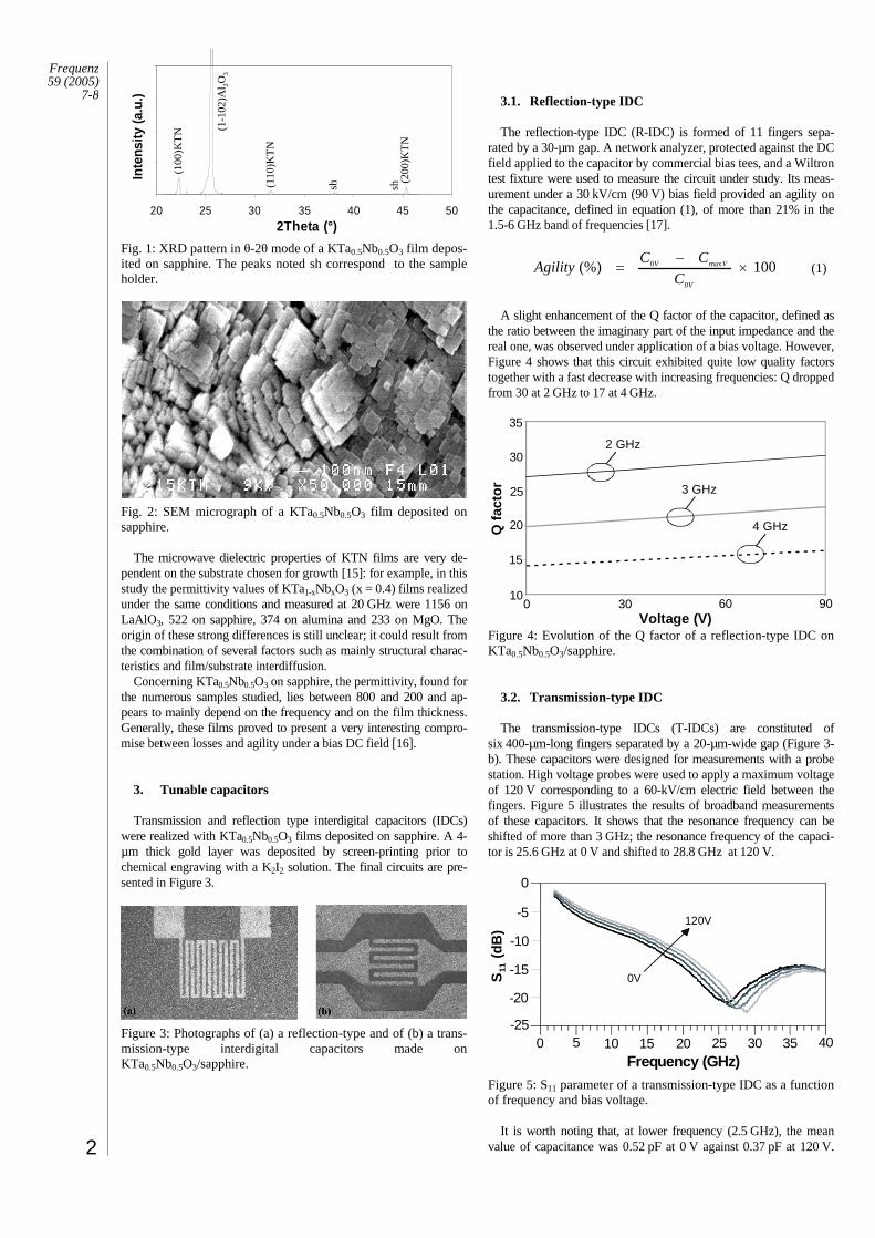
The growth of KTN on sapphire leads to a specific textured mi-crostructure formed of grains with a preferential (100) orientation associated with a minor (110) secondary orientations (Figure 1). Observations of the films with a Scanning Electron Microscope (SEM) have confirmed the texture formed of grains of size between 50 and 100 nm (Figure 2).
2
Frequenz
59 (2005)
7-8
20 25 30 35 40 45 50
2Theta (°)
Inte
nsity
(a.u
.)
(1-1
02)A
l 2O
3
(100
)KT
N
(110
)KT
N
sh sh(2
00)K
TN
20 25 30 35 40 45 502Theta (°)
Inte
nsity
(a.u
.)
(1-1
02)A
l 2O
3
(100
)KT
N
(110
)KT
N
sh sh(2
00)K
TN
Fig. 1: XRD pattern in -2 mode of a KTa0.5Nb0.5O3 film depos-ited on sapphire. The peaks noted sh correspond to the sample holder.
Fig. 2: SEM micrograph of a KTa0.5Nb0.5O3 film deposited on sapphire.
The microwave dielectric properties of KTN films are very de-pendent on the substrate chosen for growth [15]: for example, in this study the permittivity values of KTa1-xNbxO3 (x = 0.4) films realized under the same conditions and measured at 20 GHz were 1156 on LaAlO3, 522 on sapphire, 374 on alumina and 233 on MgO. The origin of these strong differences is still unclear; it could result from the combination of several factors such as mainly structural charac-teristics and film/substrate interdiffusion.
Concerning KTa0.5Nb0.5O3 on sapphire, the permittivity, found for the numerous samples studied, lies between 800 and 200 and ap-pears to mainly depend on the frequency and on the film thickness. Generally, these films proved to present a very interesting compro-mise between losses and agility under a bias DC field [16].
3. Tunable capacitors
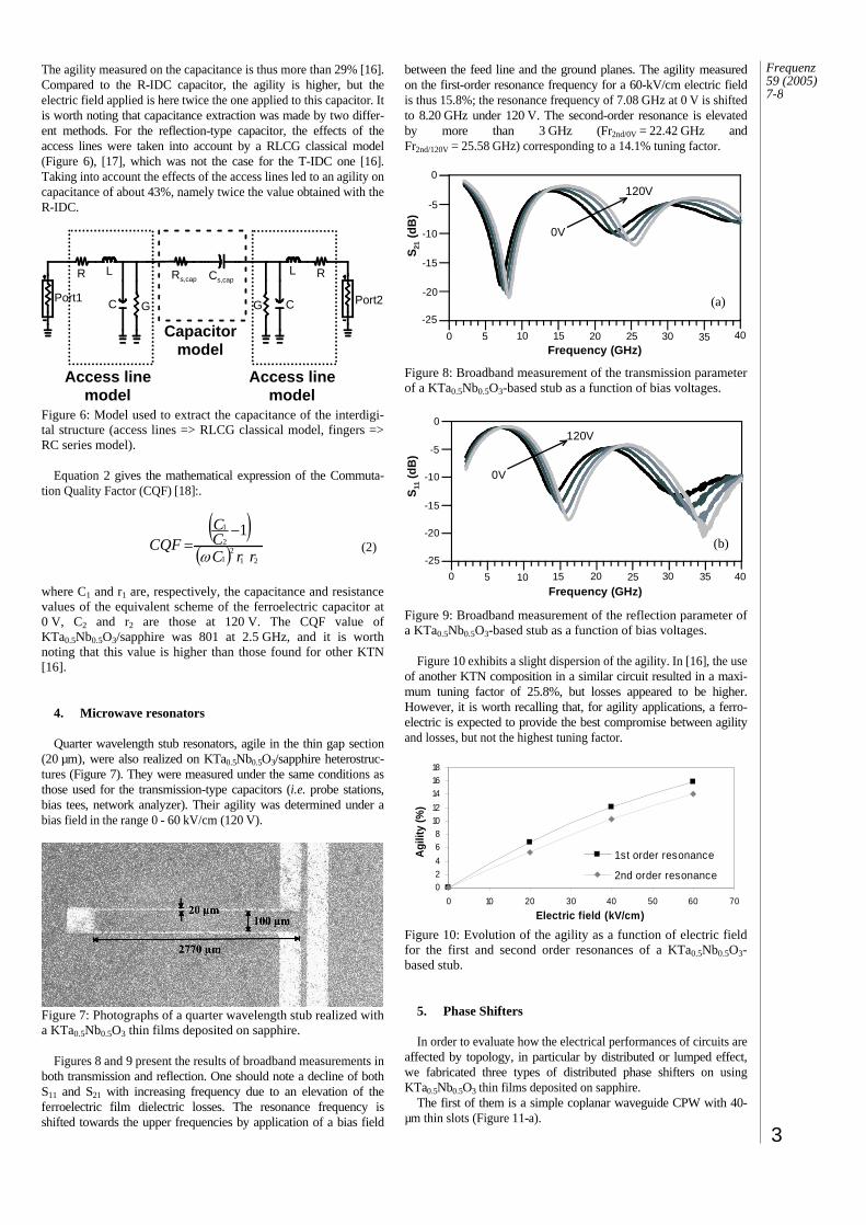
Transmission and reflection type interdigital capacitors (IDCs) were realized with KTa0.5Nb0.5O3 films deposited on sapphire. A 4-µm thick gold layer was deposited by screen-printing prior to chemical engraving with a K2I2 solution. The final circuits are pre-sented in Figure 3.
Figure 3: Photographs of (a) a reflection-type and of (b) a trans-mission-type interdigital capacitors made on KTa0.5Nb0.5O3/sapphire.
3.1. Reflection-type IDC
The reflection-type IDC (R-IDC) is formed of 11 fingers sepa-rated by a 30-µm gap. A network analyzer, protected against the DC field applied to the capacitor by commercial bias tees, and a Wiltron test fixture were used to measure the circuit under study. Its meas-urement under a 30 kV/cm (90 V) bias field provided an agility on the capacitance, defined in equation (1), of more than 21% in the 1.5-6 GHz band of frequencies [17].
100(%)0
max0
V
VV
C
CCAgility (1)
A slight enhancement of the Q factor of the capacitor, defined as the ratio between the imaginary part of the input impedance and the real one, was observed under application of a bias voltage. However, Figure 4 shows that this circuit exhibited quite low quality factors together with a fast decrease with increasing frequencies: Q dropped from 30 at 2 GHz to 17 at 4 GHz.
0 30 60 90
35
30
25
20
15
100 30 60 90
Voltage (V)
Q f
acto
r
2 GHz
3 GHz
4 GHz
Figure 4: Evolution of the Q factor of a reflection-type IDC on KTa0.5Nb0.5O3/sapphire.
3.2. Transmission-type IDC
The transmission-type IDCs (T-IDCs) are constituted of six 400-µm-long fingers separated by a 20-µm-wide gap (Figure 3-b). These capacitors were designed for measurements with a probe station. High voltage probes were used to apply a maximum voltage of 120 V corresponding to a 60-kV/cm electric field between the fingers. Figure 5 illustrates the results of broadband measurements of these capacitors. It shows that the resonance frequency can be shifted of more than 3 GHz; the resonance frequency of the capaci-tor is 25.6 GHz at 0 V and shifted to 28.8 GHz at 120 V.
S11
(d
B)
0
-5
-10
-15
-20
-250 5 10 15 20 25 30 35 40
0V
120V
Frequency (GHz) Figure 5: S11 parameter of a transmission-type IDC as a function of frequency and bias voltage.
It is worth noting that, at lower frequency (2.5 GHz), the mean value of capacitance was 0.52 pF at 0 V against 0.37 pF at 120 V.
3
Frequenz
59 (2005) 7-8
The agility measured on the capacitance is thus more than 29% [16]. Compared to the R-IDC capacitor, the agility is higher, but the electric field applied is here twice the one applied to this capacitor. It is worth noting that capacitance extraction was made by two differ-ent methods. For the reflection-type capacitor, the effects of the access lines were taken into account by a RLCG classical model (Figure 6), [17], which was not the case for the T-IDC one [16]. Taking into account the effects of the access lines led to an agility on capacitance of about 43%, namely twice the value obtained with the R-IDC.
Port1 Port2
R Rs,capR
C C
Cs,capL L
G G
Capacitor model
Access line model
Access line model
Figure 6: Model used to extract the capacitance of the interdigi-tal structure (access lines => RLCG classical model, fingers => RC series model).
Equation 2 gives the mathematical expression of the Commuta-tion Quality Factor (CQF) [18]:.
212
1
2
1 1
rrCCC
CQF
(2)
where C1 and r1 are, respectively, the capacitance and resistance values of the equivalent scheme of the ferroelectric capacitor at 0 V, C2 and r2 are those at 120 V. The CQF value of KTa0.5Nb0.5O3/sapphire was 801 at 2.5 GHz, and it is worth noting that this value is higher than those found for other KTN [16].
4. Microwave resonators
Quarter wavelength stub resonators, agile in the thin gap section (20 µm), were also realized on KTa0.5Nb0.5O3/sapphire heterostruc-tures (Figure 7). They were measured under the same conditions as those used for the transmission-type capacitors (i.e. probe stations, bias tees, network analyzer). Their agility was determined under a bias field in the range 0 - 60 kV/cm (120 V).
Figure 7: Photographs of a quarter wavelength stub realized with a KTa0.5Nb0.5O3 thin films deposited on sapphire.
Figures 8 and 9 present the results of broadband measurements in both transmission and reflection. One should note a decline of both S11 and S21 with increasing frequency due to an elevation of the ferroelectric film dielectric losses. The resonance frequency is shifted towards the upper frequencies by application of a bias field
between the feed line and the ground planes. The agility measured on the first-order resonance frequency for a 60-kV/cm electric field is thus 15.8%; the resonance frequency of 7.08 GHz at 0 V is shifted to 8.20 GHz under 120 V. The second-order resonance is elevated by more than 3 GHz (Fr2nd/0V = 22.42 GHz and Fr2nd/120V = 25.58 GHz) corresponding to a 14.1% tuning factor.
120V0
-5
-10
-15
-20
-25
S21
(d
B)
0V
0 5 10 15 20 25 30 35Frequency (GHz)
40
Figure 8: Broadband measurement of the transmission parameter of a KTa0.5Nb0.5O3-based stub as a function of bias voltages.
120V0
-5
-10
-15
-20
-25
S11
(d
B)
0V
0 5 10 15 20 25 30 35
Frequency (GHz)40
Figure 9: Broadband measurement of the reflection parameter of a KTa0.5Nb0.5O3-based stub as a function of bias voltages.
Figure 10 exhibits a slight dispersion of the agility. In [16], the use of another KTN composition in a similar circuit resulted in a maxi-mum tuning factor of 25.8%, but losses appeared to be higher. However, it is worth recalling that, for agility applications, a ferro-electric is expected to provide the best compromise between agility and losses, but not the highest tuning factor.
02
4
6
8
10
12
14
1618
0 10 20 30 40 50 60 70
Electric field (kV/cm)
Agi
lity
(%)
1st order resonance
2nd order resonance
Figure 10: Evolution of the agility as a function of electric field for the first and second order resonances of a KTa0.5Nb0.5O3-based stub.
5. Phase Shifters
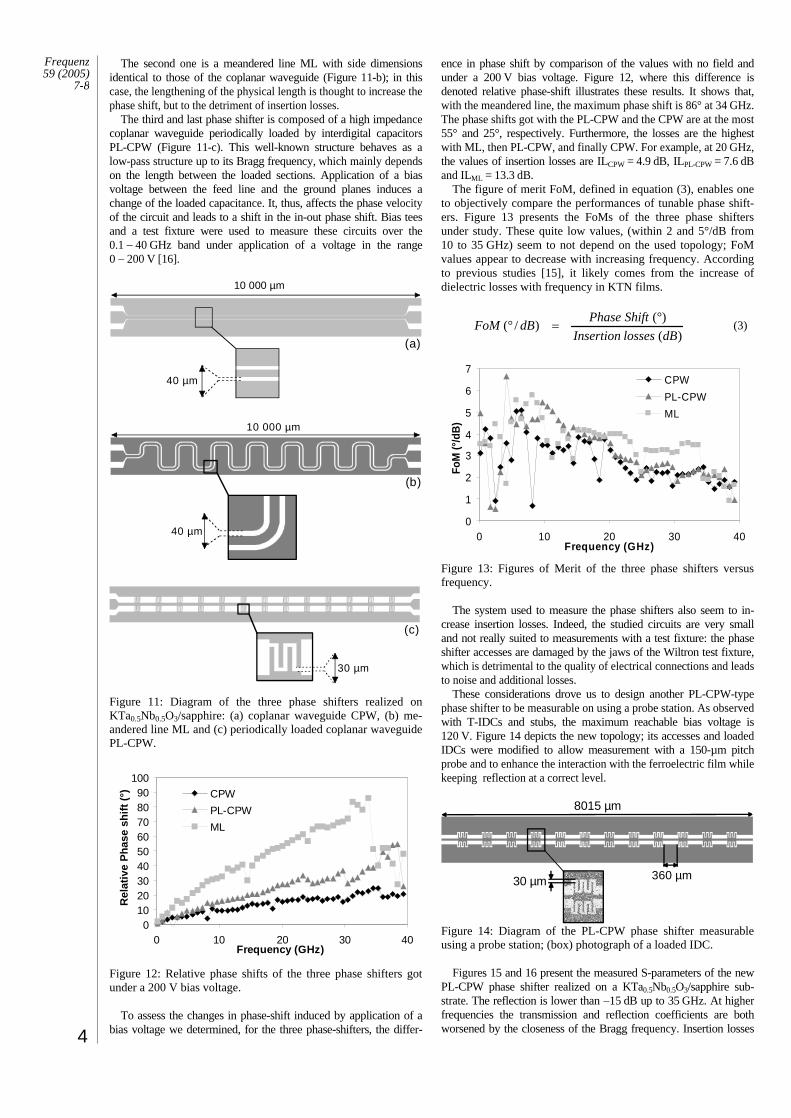
In order to evaluate how the electrical performances of circuits are affected by topology, in particular by distributed or lumped effect, we fabricated three types of distributed phase shifters on using KTa0.5Nb0.5O3 thin films deposited on sapphire.
The first of them is a simple coplanar waveguide CPW with 40-µm thin slots (Figure 11-a).
(a)
(b)
4
Frequenz
59 (2005)
7-8
The second one is a meandered line ML with side dimensions
identical to those of the coplanar waveguide (Figure 11-b); in this case, the lengthening of the physical length is thought to increase the phase shift, but to the detriment of insertion losses.
The third and last phase shifter is composed of a high impedance coplanar waveguide periodically loaded by interdigital capacitors PL-CPW (Figure 11-c). This well-known structure behaves as a low-pass structure up to its Bragg frequency, which mainly depends on the length between the loaded sections. Application of a bias voltage between the feed line and the ground planes induces a change of the loaded capacitance. It, thus, affects the phase velocity of the circuit and leads to a shift in the in-out phase shift. Bias tees and a test fixture were used to measure these circuits over the 0.1
40 GHz band under application of a voltage in the range 0
200 V [16].
10 000 µm
40 µm
40 µm
10 000 µm
30 µm
(a)
(b)
(c)
Figure 11: Diagram of the three phase shifters realized on KTa0.5Nb0.5O3/sapphire: (a) coplanar waveguide CPW, (b) me-andered line ML and (c) periodically loaded coplanar waveguide PL-CPW.
0102030405060708090
100
0 10 20 30 40Frequency (GHz)
Rel
ativ
e P
has
e sh
ift
(°) CPW
PL-CPW
ML
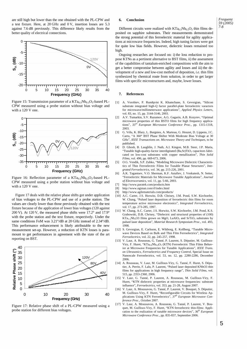
Figure 12: Relative phase shifts of the three phase shifters got under a 200 V bias voltage.
To assess the changes in phase-shift induced by application of a bias voltage we determined, for the three phase-shifters, the differ-
ence in phase shift by comparison of the values with no field and under a 200 V bias voltage. Figure 12, where this difference is denoted relative phase-shift illustrates these results. It shows that, with the meandered line, the maximum phase shift is 86° at 34 GHz. The phase shifts got with the PL-CPW and the CPW are at the most 55° and 25°, respectively. Furthermore, the losses are the highest with ML, then PL-CPW, and finally CPW. For example, at 20 GHz, the values of insertion losses are ILCPW = 4.9 dB, ILPL-CPW = 7.6 dB and ILML = 13.3 dB.
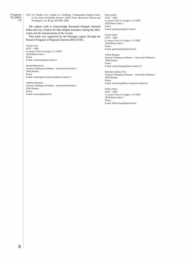
The figure of merit FoM, defined in equation (3), enables one to objectively compare the performances of tunable phase shift-ers. Figure 13 presents the FoMs of the three phase shifters under study. These quite low values, (within 2 and 5°/dB from 10 to 35 GHz) seem to not depend on the used topology; FoM values appear to decrease with increasing frequency. According to previous studies [15], it likely comes from the increase of dielectric losses with frequency in KTN films.
)(
)()/(
dBlossesInsertion
ShiftPhasedBFoM
(3)
0
1
2
3
4
5
6
7
0 10 20 30 40Frequency (GHz)
FoM
(°/d
B)
CPW
PL-CPW
ML
Figure 13: Figures of Merit of the three phase shifters versus frequency.
The system used to measure the phase shifters also seem to in-crease insertion losses. Indeed, the studied circuits are very small and not really suited to measurements with a test fixture: the phase shifter accesses are damaged by the jaws of the Wiltron test fixture, which is detrimental to the quality of electrical connections and leads to noise and additional losses.
These considerations drove us to design another PL-CPW-type phase shifter to be measurable on using a probe station. As observed with T-IDCs and stubs, the maximum reachable bias voltage is 120 V. Figure 14 depicts the new topology; its accesses and loaded IDCs were modified to allow measurement with a 150-µm pitch probe and to enhance the interaction with the ferroelectric film while keeping reflection at a correct level.
360 µm
8015 µm
30 µm
Figure 14: Diagram of the PL-CPW phase shifter measurable using a probe station; (box) photograph of a loaded IDC.
Figures 15 and 16 present the measured S-parameters of the new PL-CPW phase shifter realized on a KTa0.5Nb0.5O3/sapphire sub-strate. The reflection is lower than 15 dB up to 35 GHz. At higher frequencies the transmission and reflection coefficients are both worsened by the closeness of the Bragg frequency. Insertion losses
5
Frequenz
59 (2005) 7-8
are still high but lower than the one obtained with the PL-CPW and a test fixture. Here, at 20 GHz and 0 V, insertion losses are 5.3 against 7.6 dB previously. This difference likely results from the better quality of electrical connections.
5 10 15 20 25 30 350 40
-15
-10
-5
-20
0
S21
(d
B)
Frequency (GHz)
0V
120V
Figure 15: Transmission parameter of a KTa0.5Nb0.5O3-based PL-CPW measured using a probe station without bias voltage and with a 120 V one.
5 10 15 20 25 30 350 40
-30
-25
-20
-15
-10
-5
-35
0
Frequency (GHz)
S11
(d
B)
0V
120V
Figure 16: Reflection parameter of a KTa0.5Nb0.5O3-based PL-CPW measured using a probe station without bias voltage and with a 120 V one.
Figure 17 deals with the relative phase shifts got under application of bias voltages to the PL-CPW and use of a probe station. The values are clearly lower than those previously obtained with the test fixture because of the application of lower bias voltages (120 against 200 V). At 120 V, the measured phase shifts were 17.2° and 17.9° with the probe station and the text fixture, respectively. Under the same conditions FoM was 3.21°/dB at 20 GHz instead of 2.34°/dB. This performance enhancement is likely attributable to the new measurement set-up. However, a reduction of KTN losses is para-mount to get performances in agreement with the state of the art reporting on BST.
Rel
ativ
e P
has
e sh
ift
(°)
05
10152025303540
0 10 20 30 40Frequency (GHz)
40V
80V
120V
Figure 17: Relative phase shift of a PL-CPW measured using a probe station for different bias voltages.
6. Conclusion
Different circuits were realized with KTa0.5Nb0.5O3 thin films de-posited on sapphire substrates. Their measurements demonstrated the strong potential of this ferroelectric material for agility applica-tions at microwave frequencies. Indeed, high tuning factors were got for quite low bias fields. However, dielectric losses remained too high.
Ongoing researches are focused on: i) the loss reduction to pro-pose KTNs as a pertinent alternative to BST films, ii) the assessment of the capabilities of tantalum-enriched compositions with the aim to get a better compromise between agility and losses and iii) the de-velopment of a new and low-cost method of deposition, i.e. thin film synthesized by chemical route from solution, in order to get larger films with specific microstructures and, maybe, lower losses.
7. References
[1] A. Vorobiev, P. Rundqvist K. Khamchane, S. Gevorgian, Silicon substrate integrated high-Q factor parallel-plate ferroelectric varactors for microwave/millimeterwave applications , Applied Physics Letters, vol. 83, no. 15, pp. 3144-3146, 2003.
[2] A.V. Tumarkin, S.V. Razumov, A.G. Gagarin, A.B. Kozyrev, Optimal microwave properties of thin BSTO films for high frequency applica-tions , 33rd European Microwave Conference Proc., pp. 1315-1318, 2003.
[3] G. Vélu, K. Blary, L. Burgnies, A. Marteau, G. Houzet, D. Lippens, J.C. Carru, A 360° BST Phase Shifter With Moderate Bias Voltage at 30 GHz , IEEE Transactions on. Microwave Theory and Techniques, to be published.
[4] D. Ghosh, B. Laughlin, J. Nath, A.I. Kingon, M.B. Steer, J.P. Maria, Tunable high-quality-factor interdigitated (Ba,Sr)TiO3 capacitors fabri-
cated on low-cost substrates with copper metallization , Thin Solid Films, vol. 496, pp. 669-673, 2006.
[5] O.G. Vendik, S.P. Zubko, Modeling Microwave Dielectric Characteris-tics of Thin Ferroelectric Films for Tunable Planar Structures , Inte-grated Ferroelectrics, vol. 34, pp. 215-226, 2001.
[6] A.K. Tagantsev, V.O. Sherman, K.F. Astafiev, J. Venkatesh, N. Setter, Ferroelectric Materials for Microwave Tunable Applications , Journal
of Electroceramics, vol. 11, pp. 5-66, 2003. [7] http://www.paratek.com/products.htm [8] http://www.ngimat.com/rf/index.html [9] http://www.agilematerials.com/products/ [10] A.C. Carter, J.S. Horwitz, D.B. Chrisey, J.M. Pond, S.W. Kirchoefer,
W. Chang, Pulsed laser deposition of ferroelectric thin films for room temperature active microwave electronics , Integrated Ferroelectrics, vol. 17, pp. 273-285, 1997.
[11] W. Chang, A.C. Carter, J.S. Horwitz, S.W. Kirchoefer, J.M. Pond, K.S. Grabowski, D.B. Chrisey, Dielectric and structural properties of (100) KTa1-xNbxO3 films grown on MgO, LaAlO3 and SrTiO3 substrates by pulsed laser deposition , Material Research Symposium Proc., vol. 493, 1998.
[12] S. Gevorgian, E. Carlsson, E. Wikborg, E. Kollberg, Tunable Micro-wave Devices Based on Bulk and Thin Film Ferroelectrics , Integrated Ferroelectrics, vol. 22, pp. 245-257, 1998.
[13] V. Laur, A. Rousseau, G. Tanné, P. Laurent, S. Députier, M. Guilloux-Viry, F. Huret, KTa0.6Nb0.4O3 (KTN) Ferroelectric Thin Films Behav-ior at Microwave Frequencies for Tunable Applications , IEEE Trans. on Ultrasonics, Ferroelectrics and Frequency Control, Special Issue on Nanoscale Ferroelectrics, vol. 53, no. 12, pp. 2280-2286, December 2006.
[14] A. Rousseau, V. Laur, M. Guilloux-Viry, G. Tanné, F. Huret, S. Dépu-tier, A. Perrin, F. Lalu, P. Laurent, Pulsed laser deposited KNbO3 thin films for applications in high frequency range , Thin Solid Films, vol. 515, pp. 2353-2360, 2006.
[15] V. Laur, G. Tanné, P. Laurent, A. Rousseau, M. Guilloux-Viry, F. Huret, KTN dielectric properties at microwave frequencies: substrate influence , Ferroelectrics, vol. 353, pp. 21-28, August 2007.
[16] V. Laur, A. Moussavou, G. Tanné, P. Laurent, V. Bouquet, S. Députier, M. Guilloux-Viry, F. Huret, Reconfigurable Circuits for Wireless Ap-plications Using KTN Ferroelectrics , 37th European Microwave Con-ference Proc., Octobre 2007.
[17] V. Laur, A. Moussavou, A. Rousseau, G. Tanné, P. Laurent, V. Bou-quet, M. Guilloux-Viry, F. Huret, KTN ferroelectric thin-films: Appli-cation to the realization of tunable microwave devices , 36th European Microwave Conference Proc., pp. 835-837, Septembre 2006.
6
Frequenz
59 (2005)
7-8
[18] I.B. Vendik, O.G. Vendik, E.L. Kollberg, Commutation Quality Factor
of Two-State Switchable devices , IEEE Trans. Microwave Theory and Techniques, vol. 48, pp. 802-808, 2000.
The authors wish to acknowledge Raymond Jézéquel, Bernard Della and Guy Chuiton for their helpful assistance during the fabri-cation and the measurements of the circuits.
This study was supported by the Bretagne region through the Resarch Program of Regional Interest DISCOTEC.
Vincent Laur LEST UBO, 6, avenue Victor Le Gorgeu, C.S. 93837 29238 Brest Cedex 3 France E-mail: [email protected]
Arnaud Moussavou Sciences Chimiques de Rennes Université de Rennes I 35042 Rennes France E-mail: [email protected]
Anthony Rousseau Sciences Chimiques de Rennes Université de Rennes I 35042 Rennes France E-mail: [email protected]
Paul Laurent LEST UBO, 6, avenue Victor Le Gorgeu, C.S. 93837 29238 Brest Cedex 3 France E-mail: [email protected]
Gérard Tanné LEST UBO, 6, avenue Victor Le Gorgeu, C.S. 93837 29238 Brest Cedex 3 France E-mail: [email protected]
Valérie Bouquet Sciences Chimiques de Rennes
Université de Rennes I 35042 Rennes France E-mail: [email protected]
Maryline Guilloux-Viry Sciences Chimiques de Rennes Université de Rennes I 35042 Rennes France E-mail: [email protected]
Fabrice Huret LEST UBO, 6, avenue Victor Le Gorgeu, C.S. 93837 29238 Brest Cedex 3 France E-mail: [email protected]


![Manganese-NanoparticlesSubstitutionsontheVanadiumSitesof Bi … · 2017. 7. 24. · ment of ferroelectric properties together with a lowered processing temperature [15, 16]. It has](https://img.pdfslide.net/doc/110x75/610263232d8c8c2416030878/manganese-nanoparticlessubstitutionsonthevanadiumsitesof-bi-2017-7-24-ment.jpg)


![FERROELECTRIC RAM [FRAM] - Study Mafiastudymafia.org/wp...FERROELECTRIC-RAM-FRAM-Report.pdf · A Seminar report On FERROELECTRIC RAM [FRAM] Submitted in partial fulfillment of the](https://img.pdfslide.net/doc/110x75/5b94f2f009d3f2130d8dd6e1/ferroelectric-ram-fram-study-a-seminar-report-on-ferroelectric-ram-fram.jpg)


![Manganese-NanoparticlesSubstitutionsontheVanadiumSitesof Bi … · 2019. 7. 31. · ment of ferroelectric properties together with a lowered processing temperature [15, 16]. It has](https://img.pdfslide.net/doc/110x75/61025fb7de28726cae024e1a/manganese-nanoparticlessubstitutionsonthevanadiumsitesof-bi-2019-7-31-ment.jpg)


![Sangeetha [Ferroelectric Memory]](https://img.pdfslide.net/doc/110x75/55cf8f91550346703b9d9665/sangeetha-ferroelectric-memory.jpg)