Embed Size (px)
Citation preview
2
.
This chapter introduces the mixer circuit and shows all the basicsof DC simulations, including a family of curves and device biasingcalculations.
Lab 2: DC Simulations
Lab 2: DC Simulations
2-2
OBJECTIVES
• Build a symbolized sub-circuit for use in the hierarchy
• Create a family of curves for the device used in the mixer
• Sweep variables, pass parameters, and the plot or list the data
• Use equations to calculate bias resistor values from simulation data
NOTE about this lab: This lab and the remaining labs will use the BJT mixer todemonstrate all types of simulations. Regardless of the type of circuit you design, thetechniques and simulations presented in these labs will be applicable to many othercircuit configurations.
PROCEDURE
The following steps are for creating the mixer BJT sub-circuit with package parasiticsand performing the dc simulations as part of the design process.
1. Create a New Project and name it: mixer
2. Open a New Schematic Window and save it as: bjt_pkg
3. Setup the BJT device and model:
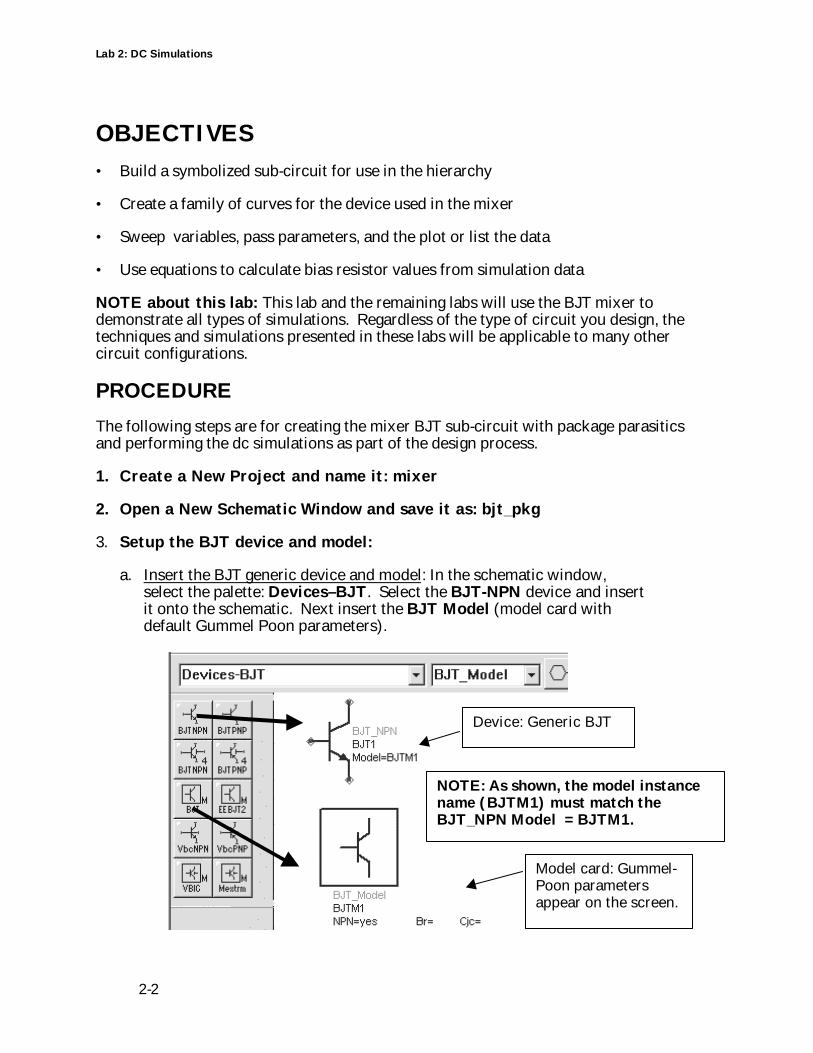
a. Insert the BJT generic device and model: In the schematic window,select the palette: Devices–BJT. Select the BJT-NPN device and insertit onto the schematic. Next insert the BJT Model (model card withdefault Gummel Poon parameters).
Device: Generic BJT
Model card: Gummel-Poon parametersappear on the screen.
NOTE: As shown, the model instancename (BJTM1) must match theBJT_NPN Model = BJTM1.
Lab 2: DC Simulations
2-3
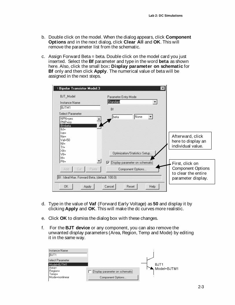
b. Double click on the model. When the dialog appears, click ComponentOptions and in the next dialog, click Clear All and OK. This willremove the parameter list from the schematic.
c. Assign Forward Beta = beta. Double click on the model card you justinserted. Select the Bf parameter and type in the word beta as shownhere. Also, click the small box: Display parameter on schematic forBf only and then click Apply. The numerical value of beta will beassigned in the next steps.
d. Type in the value of Vaf (Forward Early Voltage) as 50 and display it byclicking Apply and OK. This will make the dc curves more realistic.
e. Click OK to dismiss the dialog box with these changes.
f. For the BJT device or any component, you can also remove theunwanted display parameters (Area, Region, Temp and Mode) by editingit in the same way.
First, click onComponent Optionsto clear the entireparameter display.
Afterward, clickhere to display anindividual value.
Lab 2: DC Simulations
2-4
4. Build the rest of the subcircuit
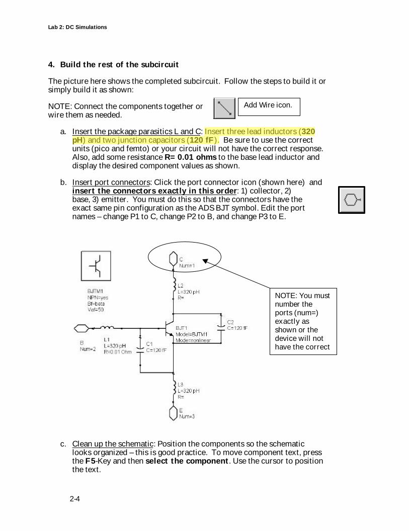
The picture here shows the completed subcircuit. Follow the steps to build it orsimply build it as shown:
NOTE: Connect the components together orwire them as needed.
a. Insert the package parasitics L and C: Insert three lead inductors (320pH) and two junction capacitors (120 fF). Be sure to use the correctunits (pico and femto) or your circuit will not have the correct response.Also, add some resistance R= 0.01 ohms to the base lead inductor anddisplay the desired component values as shown.
b. Insert port connectors: Click the port connector icon (shown here) andinsert the connectors exactly in this order: 1) collector, 2)base, 3) emitter. You must do this so that the connectors have theexact same pin configuration as the ADS BJT symbol. Edit the portnames – change P1 to C, change P2 to B, and change P3 to E.
c. Clean up the schematic: Position the components so the schematiclooks organized – this is good practice. To move component text, pressthe F5-Key and then select the component. Use the cursor to positionthe text.
Add Wire icon.
NOTE: You mustnumber theports (num=)exactly asshown or thedevice will nothave the correctorientation.

Lab 2: DC Simulations
2-5
5. Create a symbol for the sub-circuit
There are three ways to create a symbol for a circuit: 1) Use a defaultsymbol, 2) Use a built-in symbol (a standard symbol), or 3) Create a newsymbol by drawing one or modifying an existing one. For this lab you willuse a built-in bjt symbol which looks better than the default three-portsymbol. The following steps shows how to do this:
a. To see the default symbol, click: View >Create/Edit Schematic Symbol. The symbolpage will replace the schematic page and a dialogwill appear. Click OK to use the defaults.
b. Next, a rectangle or square with three ports isgenerated:
NOTE: You will be replacing the default symbol with a built-inBJT symbol in the next steps. As you do, you must assign thepin (port) numbers exactly as shown to match the built-insymbol for the emitter, base, and collector.
c. To change the symbol to a built-in symbol that looks like atransistor, delete the entire symbol you just created: Select > SelectAll. Then click the trash can icon to delete the symbol.
d. Return to the schematic: View > Create/Edit Schematic.Now click File> Design Parameters. In the General tab,there is a Symbol Name parameter list. Click the arrow andselect: SYM_BJT_NPN. Also, Change the componentinstance name to Q.
File >Design Parameters
Lab 2: DC Simulations
2-6
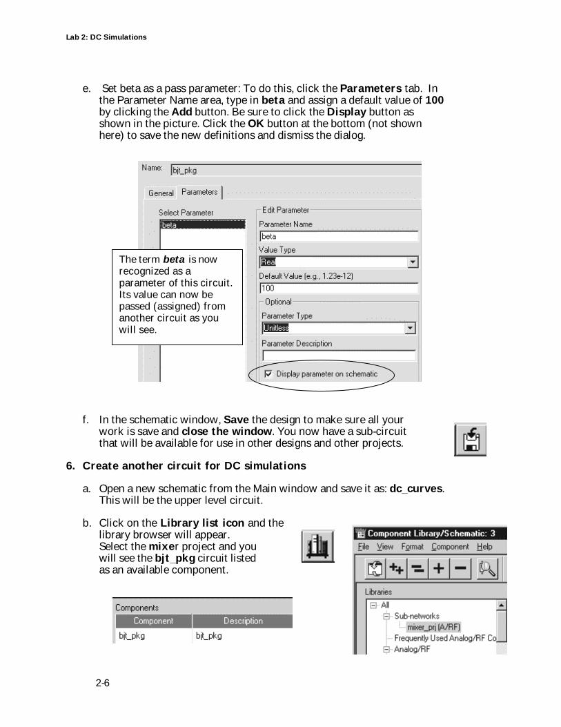
e. Set beta as a pass parameter: To do this, click the Parameters tab. Inthe Parameter Name area, type in beta and assign a default value of 100by clicking the Add button. Be sure to click the Display button asshown in the picture. Click the OK button at the bottom (not shownhere) to save the new definitions and dismiss the dialog.
f. In the schematic window, Save the design to make sure all yourwork is save and close the window. You now have a sub-circuitthat will be available for use in other designs and other projects.
6. Create another circuit for DC simulations
a. Open a new schematic from the Main window and save it as: dc_curves.This will be the upper level circuit.
b. Click on the Library list icon and thelibrary browser will appear.Select the mixer project and youwill see the bjt_pkg circuit listedas an available component.
The term beta is nowrecognized as aparameter of this circuit.Its value can now bepassed (assigned) fromanother circuit as youwill see.
Lab 2: DC Simulations
2-7
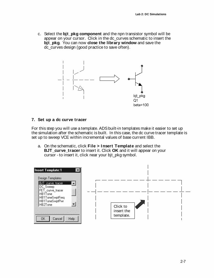
c. Select the bjt_pkg component and the npn transistor symbol will beappear on your cursor. Click in the dc_curves schematic to insert thebjt_pkg. You can now close the library window and save thedc_curves design (good practice to save often).
7. Set up a dc curve tracer
For this step you will use a template. ADS built-in templates make it easier to set upthe simulation after the schematic is built. In this case, the dc curve tracer template isset up to sweep VCE within incremental values of base current IBB.
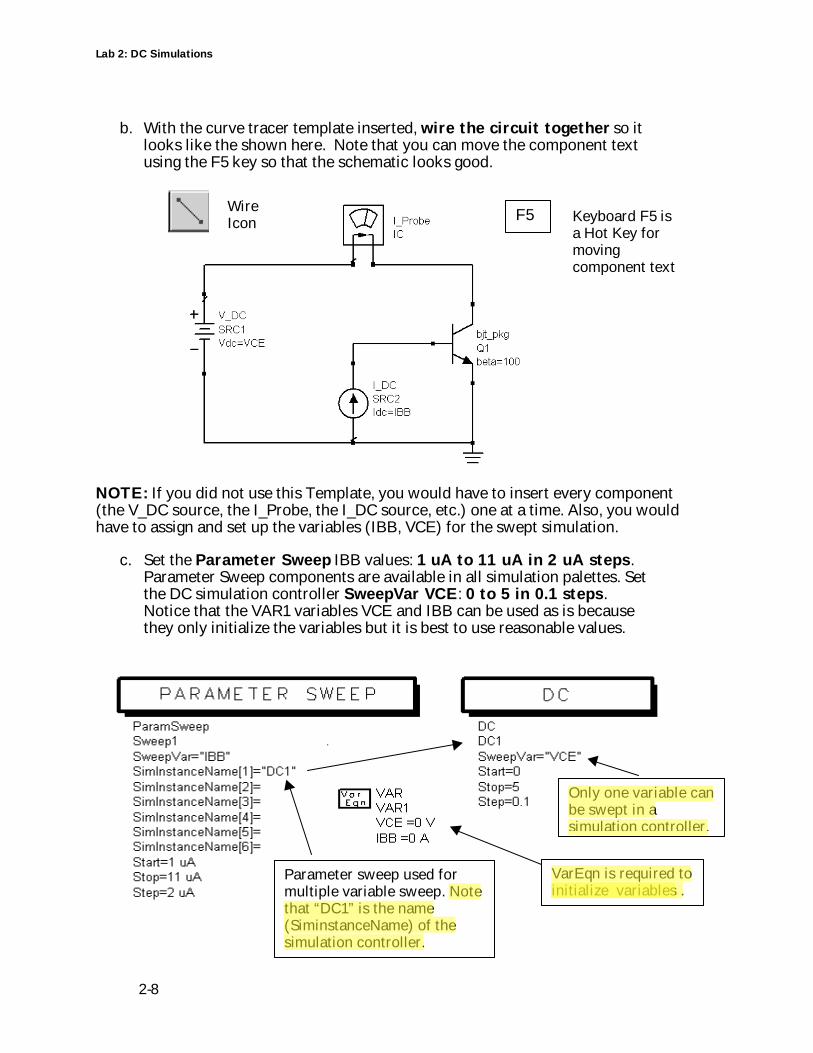
a. On the schematic, click File > Insert Template and select theBJT_curve_tracer to insert it. Click OK and it will appear on yourcursor - to insert it, click near your bjt_pkg symbol.
Click toinsert thetemplate.
Lab 2: DC Simulations
2-8
b. With the curve tracer template inserted, wire the circuit together so itlooks like the shown here. Note that you can move the component textusing the F5 key so that the schematic looks good.
NOTE: If you did not use this Template, you would have to insert every component(the V_DC source, the I_Probe, the I_DC source, etc.) one at a time. Also, you wouldhave to assign and set up the variables (IBB, VCE) for the swept simulation.
c. Set the Parameter Sweep IBB values: 1 uA to 11 uA in 2 uA steps.Parameter Sweep components are available in all simulation palettes. Setthe DC simulation controller SweepVar VCE: 0 to 5 in 0.1 steps.Notice that the VAR1 variables VCE and IBB can be used as is becausethey only initialize the variables but it is best to use reasonable values.
Parameter sweep used formultiple variable sweep. Notethat “DC1” is the name(SiminstanceName) of thesimulation controller.
VarEqn is required toinitialize variables .
Only one variable canbe swept in asimulation controller.
F5WireIcon Keyboard F5 is
a Hot Key formovingcomponent text
Lab 2: DC Simulations
2-9
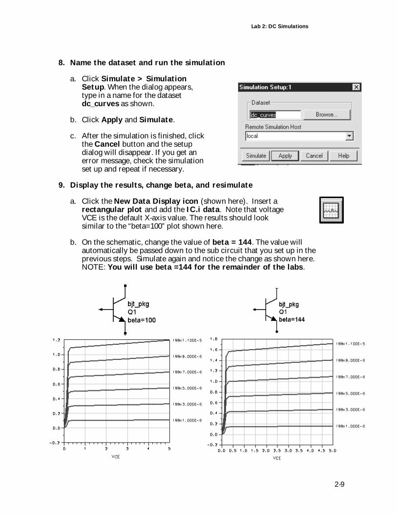
8. Name the dataset and run the simulation
a. Click Simulate > SimulationSetup. When the dialog appears,type in a name for the datasetdc_curves as shown.
b. Click Apply and Simulate.
c. After the simulation is finished, clickthe Cancel button and the setupdialog will disappear. If you get anerror message, check the simulationset up and repeat if necessary.
9. Display the results, change beta, and resimulate
a. Click the New Data Display icon (shown here). Insert arectangular plot and add the IC.i data. Note that voltageVCE is the default X-axis value. The results should looksimilar to the “beta=100” plot shown here.
b. On the schematic, change the value of beta = 144. The value willautomatically be passed down to the sub circuit that you set up in theprevious steps. Simulate again and notice the change as shown here.NOTE: You will use beta =144 for the remainder of the labs.
Lab 2: DC Simulations
2-10
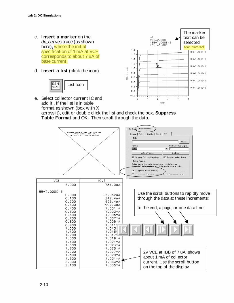
c. Insert a marker on thedc_curves trace (as shownhere), where the initialspecification of 1 mA at VCEcorresponds to about 7 uA ofbase current.
d. Insert a list (click the icon).
e. Select collector current IC andadd it . If the list is in tableformat as shown (box with Xacross it), edit or double click the list and check the box, SuppressTable Format and OK. Then scroll through the data.
The markertext can beselectedand moved.
2V VCE at IBB of 7 uA showsabout 1 mA of collectorcurrent. Use the scroll buttonon the top of the display
Use the scroll buttons to rapidly movethrough the data at these increments:
to the end, a page, or one data line.
List Icon
Lab 2: DC Simulations
2-11
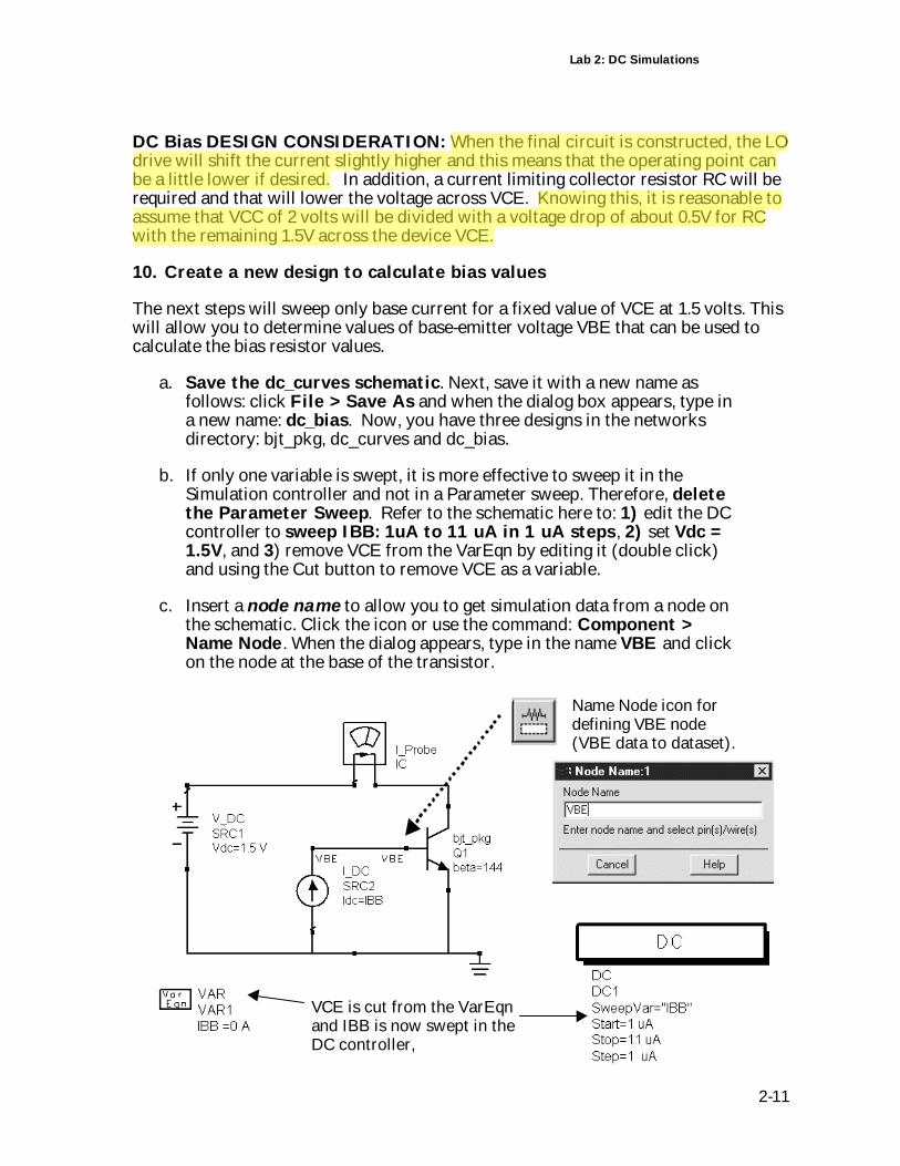
DC Bias DESIGN CONSIDERATION: When the final circuit is constructed, the LOdrive will shift the current slightly higher and this means that the operating point canbe a little lower if desired. In addition, a current limiting collector resistor RC will berequired and that will lower the voltage across VCE. Knowing this, it is reasonable toassume that VCC of 2 volts will be divided with a voltage drop of about 0.5V for RCwith the remaining 1.5V across the device VCE.
10. Create a new design to calculate bias values
The next steps will sweep only base current for a fixed value of VCE at 1.5 volts. Thiswill allow you to determine values of base-emitter voltage VBE that can be used tocalculate the bias resistor values.
a. Save the dc_curves schematic. Next, save it with a new name asfollows: click File > Save As and when the dialog box appears, type ina new name: dc_bias. Now, you have three designs in the networksdirectory: bjt_pkg, dc_curves and dc_bias.
b. If only one variable is swept, it is more effective to sweep it in theSimulation controller and not in a Parameter sweep. Therefore, deletethe Parameter Sweep. Refer to the schematic here to: 1) edit the DCcontroller to sweep IBB: 1uA to 11 uA in 1 uA steps, 2) set Vdc =1.5V, and 3) remove VCE from the VarEqn by editing it (double click)and using the Cut button to remove VCE as a variable.
c. Insert a node name to allow you to get simulation data from a node onthe schematic. Click the icon or use the command: Component >Name Node. When the dialog appears, type in the name VBE and clickon the node at the base of the transistor.
Name Node icon fordefining VBE node(VBE data to dataset).
VCE is cut from the VarEqnand IBB is now swept in theDC controller,
Lab 2: DC Simulations
2-12
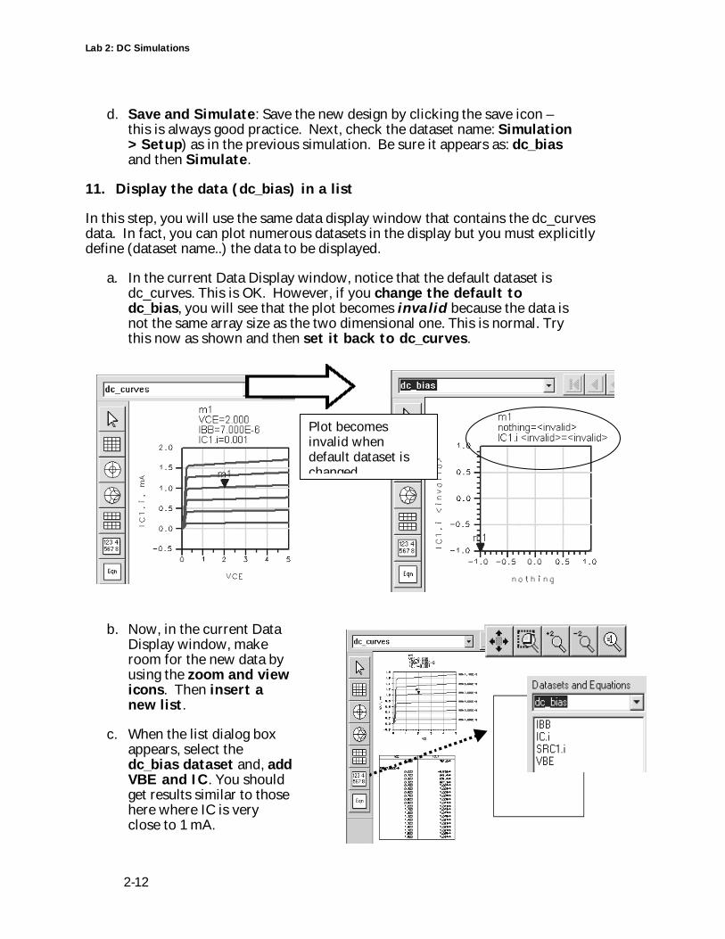
d. Save and Simulate: Save the new design by clicking the save icon –this is always good practice. Next, check the dataset name: Simulation> Setup) as in the previous simulation. Be sure it appears as: dc_biasand then Simulate.
11. Display the data (dc_bias) in a list
In this step, you will use the same data display window that contains the dc_curvesdata. In fact, you can plot numerous datasets in the display but you must explicitlydefine (dataset name..) the data to be displayed.
a. In the current Data Display window, notice that the default dataset isdc_curves. This is OK. However, if you change the default todc_bias, you will see that the plot becomes invalid because the data isnot the same array size as the two dimensional one. This is normal. Trythis now as shown and then set it back to dc_curves.
b. Now, in the current DataDisplay window, makeroom for the new data byusing the zoom and viewicons. Then insert anew list.
c. When the list dialog boxappears, select thedc_bias dataset and, addVBE and IC. You shouldget results similar to thosehere where IC is veryclose to 1 mA.
Plot becomesinvalid whendefault dataset ischanged.
Lab 2: DC Simulations
2-13
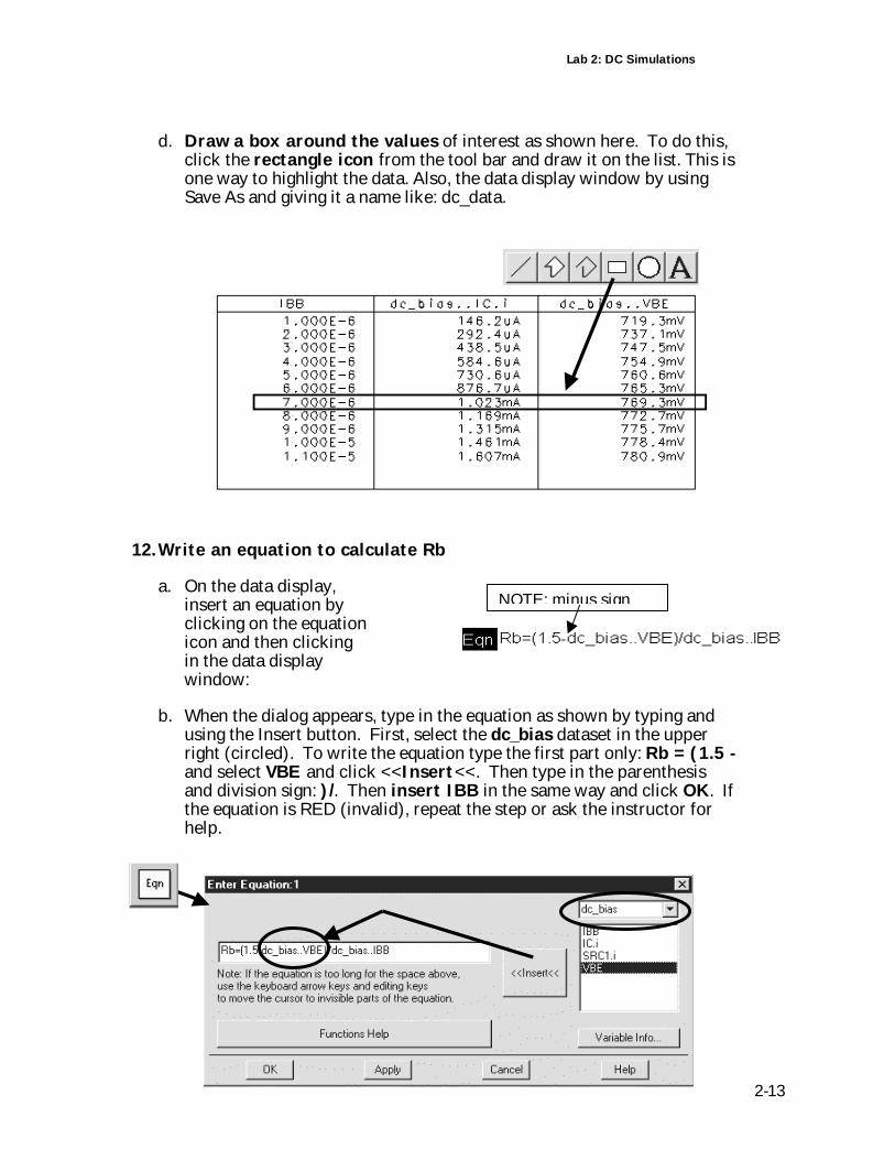
d. Draw a box around the values of interest as shown here. To do this,click the rectangle icon from the tool bar and draw it on the list. This isone way to highlight the data. Also, the data display window by usingSave As and giving it a name like: dc_data.
12. Write an equation to calculate Rb
a. On the data display,insert an equation byclicking on the equationicon and then clickingin the data displaywindow:
b. When the dialog appears, type in the equation as shown by typing andusing the Insert button. First, select the dc_bias dataset in the upperright (circled). To write the equation type the first part only: Rb = (1.5 -and select VBE and click <<Insert<<. Then type in the parenthesisand division sign: )/. Then insert IBB in the same way and click OK. Ifthe equation is RED (invalid), repeat the step or ask the instructor forhelp.
NOTE: minus sign
Lab 2: DC Simulations
2-14
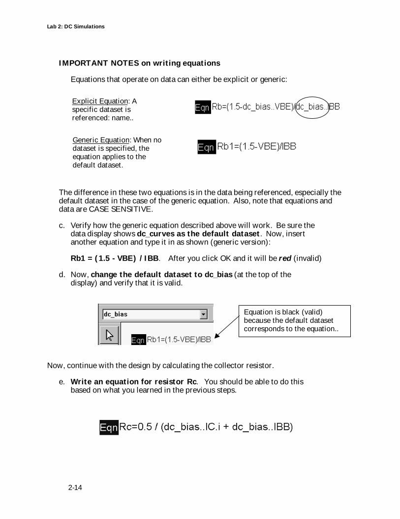
IMPORTANT NOTES on writing equations
Equations that operate on data can either be explicit or generic:
The difference in these two equations is in the data being referenced, especially thedefault dataset in the case of the generic equation. Also, note that equations anddata are CASE SENSITIVE.
c. Verify how the generic equation described above will work. Be sure thedata display shows dc_curves as the default dataset. Now, insertanother equation and type it in as shown (generic version):
Rb1 = (1.5 - VBE) / IBB. After you click OK and it will be red (invalid)
d. Now, change the default dataset to dc_bias (at the top of thedisplay) and verify that it is valid.
Now, continue with the design by calculating the collector resistor.
e. Write an equation for resistor Rc. You should be able to do thisbased on what you learned in the previous steps.
Generic Equation: When nodataset is specified, theequation applies to thedefault dataset.
Explicit Equation: Aspecific dataset isreferenced: name..
Equation is black (valid)because the default datasetcorresponds to the equation..
Lab 2: DC Simulations
2-15
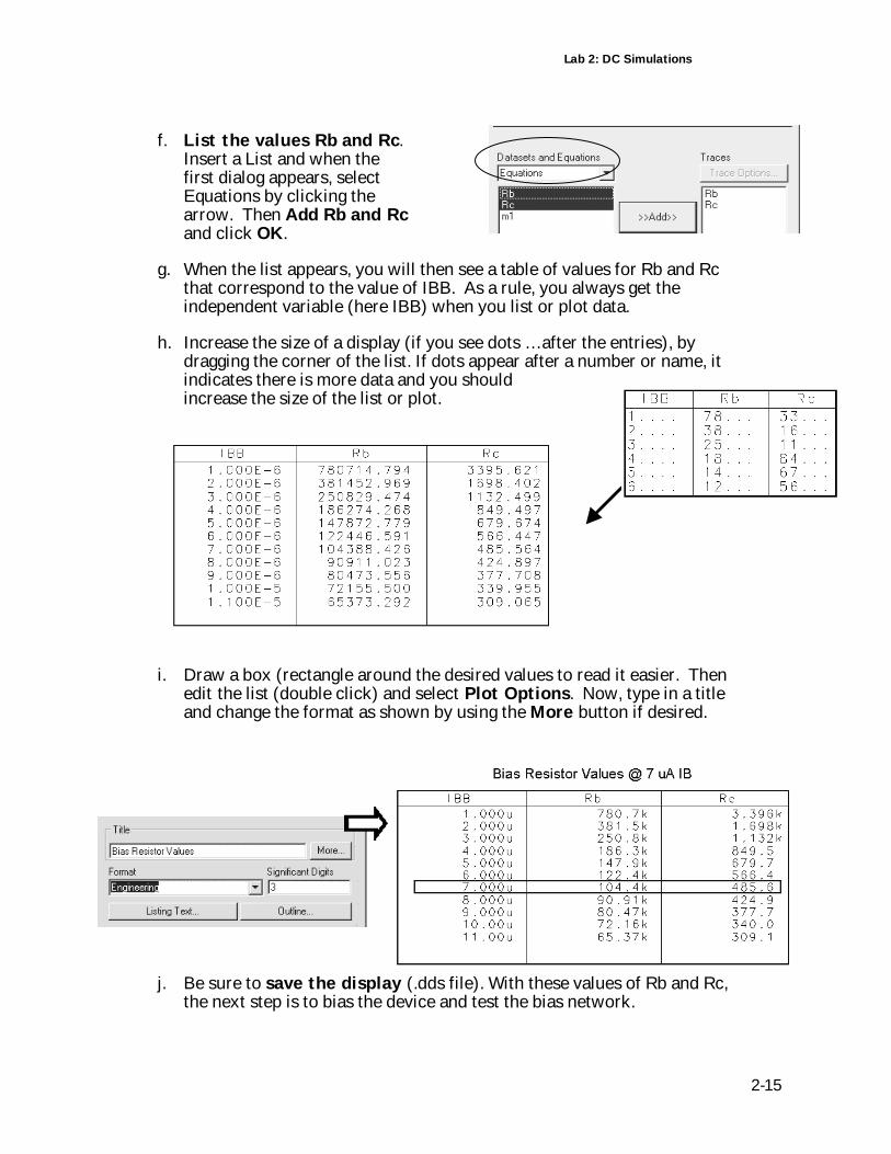
f. List the values Rb and Rc.Insert a List and when thefirst dialog appears, selectEquations by clicking thearrow. Then Add Rb and Rcand click OK.
g. When the list appears, you will then see a table of values for Rb and Rcthat correspond to the value of IBB. As a rule, you always get theindependent variable (here IBB) when you list or plot data.
h. Increase the size of a display (if you see dots …after the entries), bydragging the corner of the list. If dots appear after a number or name, itindicates there is more data and you shouldincrease the size of the list or plot.
i. Draw a box (rectangle around the desired values to read it easier. Thenedit the list (double click) and select Plot Options. Now, type in a titleand change the format as shown by using the More button if desired.
j. Be sure to save the display (.dds file). With these values of Rb and Rc,the next step is to bias the device and test the bias network.
Lab 2: DC Simulations
2-16
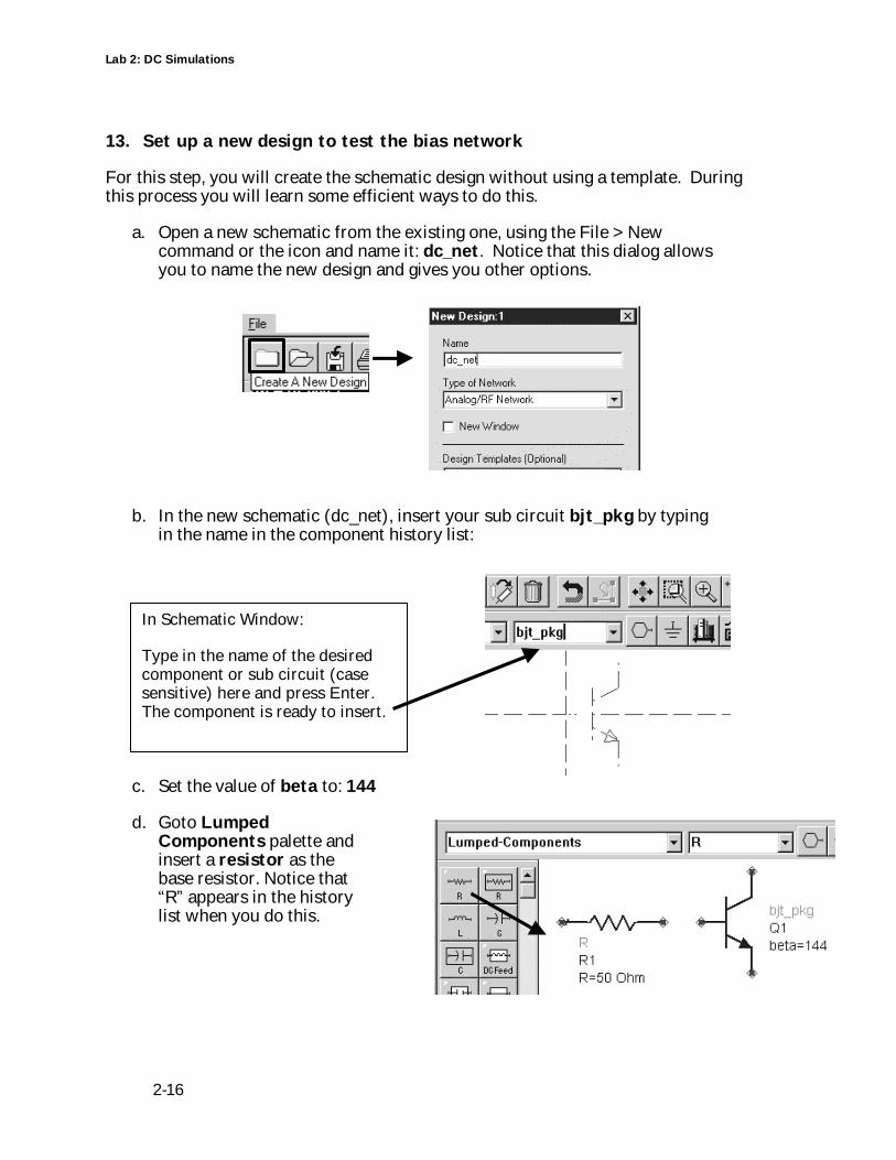
13. Set up a new design to test the bias network
For this step, you will create the schematic design without using a template. Duringthis process you will learn some efficient ways to do this.
a. Open a new schematic from the existing one, using the File > Newcommand or the icon and name it: dc_net. Notice that this dialog allowsyou to name the new design and gives you other options.
b. In the new schematic (dc_net), insert your sub circuit bjt_pkg by typingin the name in the component history list:
c. Set the value of beta to: 144
d. Goto LumpedComponents palette andinsert a resistor as thebase resistor. Notice that“R” appears in the historylist when you do this.
In Schematic Window:
Type in the name of the desiredcomponent or sub circuit (casesensitive) here and press Enter.The component is ready to insert.
Lab 2: DC Simulations
2-17
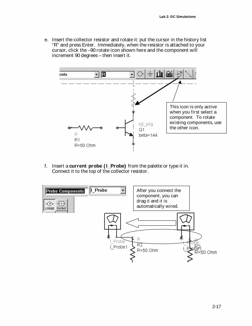
e. Insert the collector resistor and rotate it: put the cursor in the history list“R” and press Enter. Immediately, when the resistor is attached to yourcursor, click the –90 rotate icon shown here and the component willincrement 90 degrees – then insert it.
f. Insert a current probe (I_Probe) from the palette or type it in.Connect it to the top of the collector resistor.
After you connect thecomponent, you candrag it and it isautomatically wired.
This icon is only activewhen you first select acomponent. To rotateexisting components, usethe other icon.
Lab 2: DC Simulations
2-18
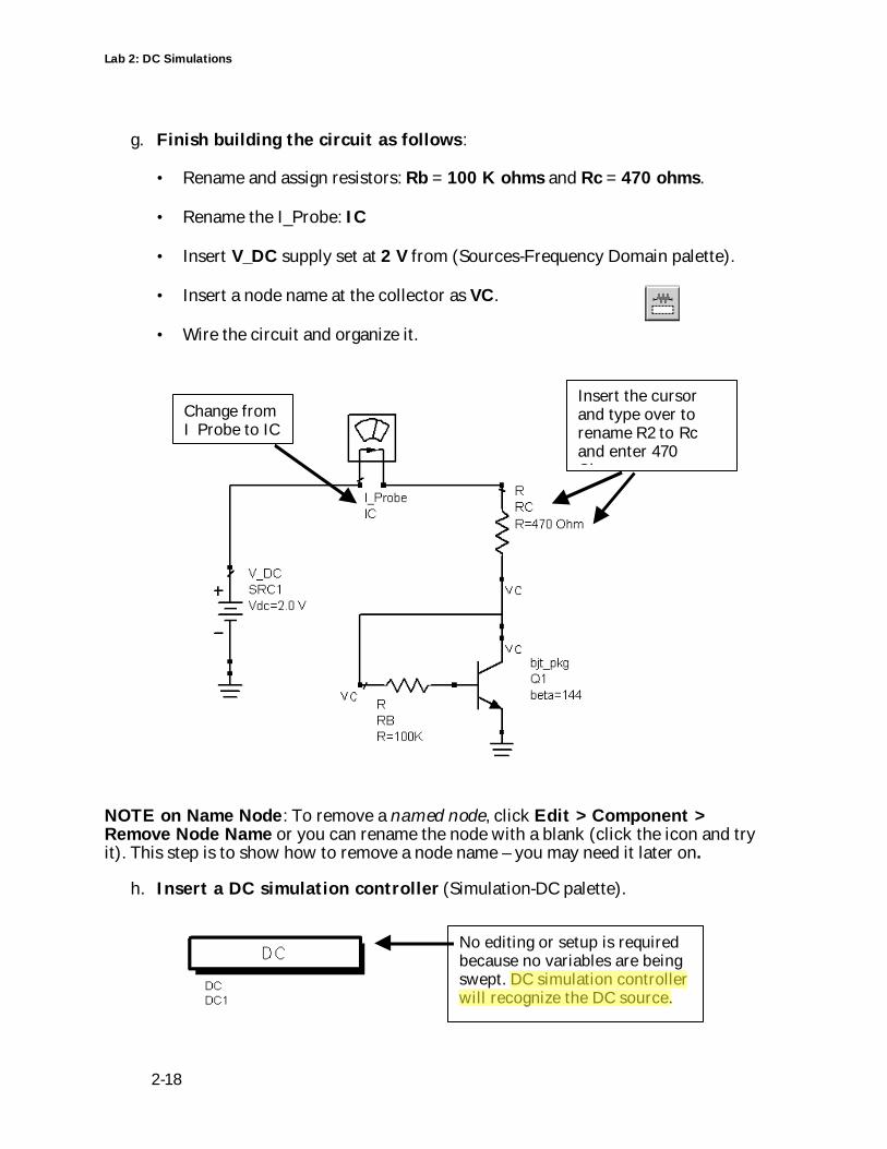
g. Finish building the circuit as follows:
• Rename and assign resistors: Rb = 100 K ohms and Rc = 470 ohms.
• Rename the I_Probe: IC
• Insert V_DC supply set at 2 V from (Sources-Frequency Domain palette).
• Insert a node name at the collector as VC.
• Wire the circuit and organize it.
NOTE on Name Node: To remove a named node, click Edit > Component >Remove Node Name or you can rename the node with a blank (click the icon and tryit). This step is to show how to remove a node name – you may need it later on.
h. Insert a DC simulation controller (Simulation-DC palette).
No editing or setup is requiredbecause no variables are beingswept. DC simulation controllerwill recognize the DC source.
Change fromI_Probe to IC
Insert the cursorand type over torename R2 to Rcand enter 470Ohms.
Lab 2: DC Simulations
2-19
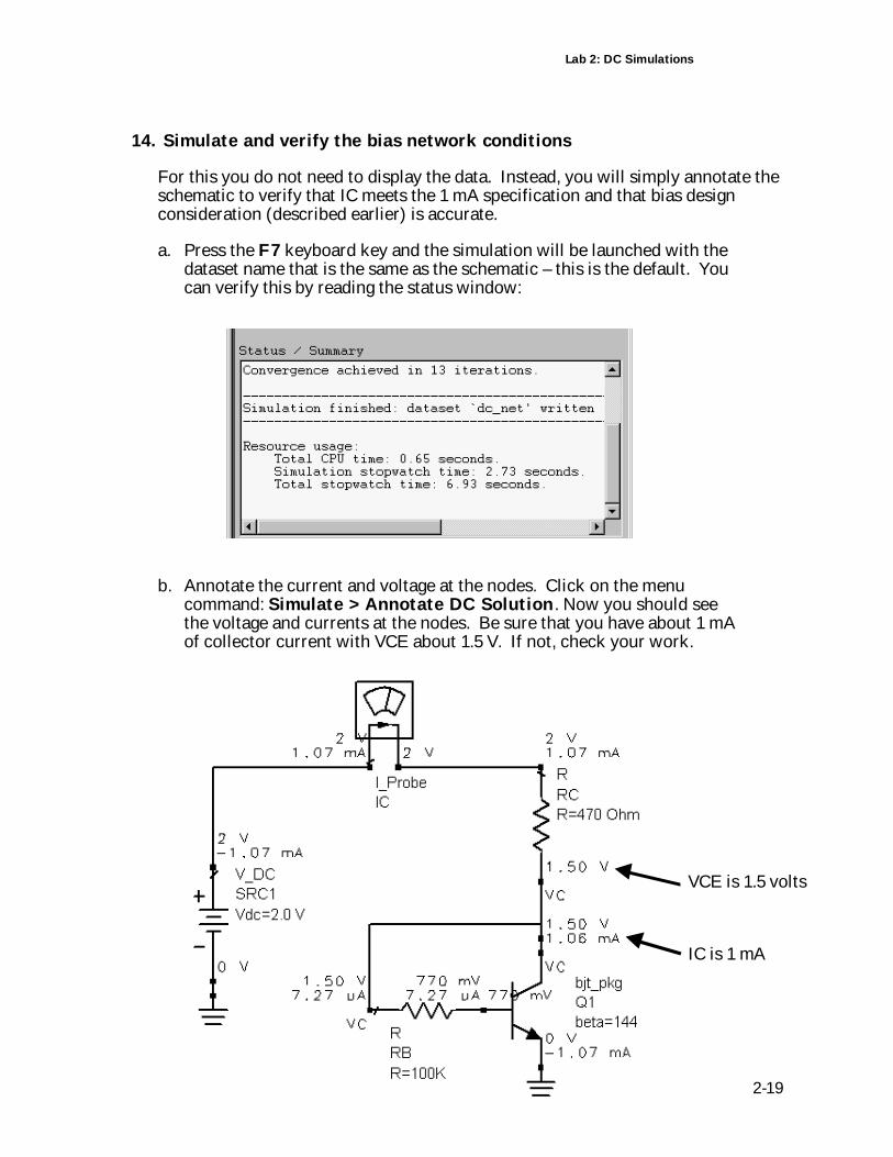
14. Simulate and verify the bias network conditions
For this you do not need to display the data. Instead, you will simply annotate theschematic to verify that IC meets the 1 mA specification and that bias designconsideration (described earlier) is accurate.
a. Press the F7 keyboard key and the simulation will be launched with thedataset name that is the same as the schematic – this is the default. Youcan verify this by reading the status window:
b. Annotate the current and voltage at the nodes. Click on the menucommand: Simulate > Annotate DC Solution. Now you should seethe voltage and currents at the nodes. Be sure that you have about 1 mAof collector current with VCE about 1.5 V. If not, check your work.
VCE is 1.5 volts
IC is 1 mA
Lab 2: DC Simulations
2-20
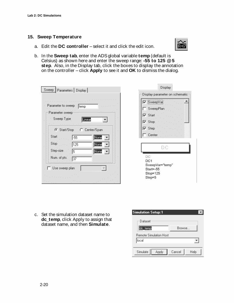
15. Sweep Temperature
a. Edit the DC controller – select it and click the edit icon.
b. In the Sweep tab, enter the ADS global variable temp (default isCelsius) as shown here and enter the sweep range: -55 to 125 @ 5step. Also, in the Display tab, click the boxes to display the annotationon the controller – click Apply to see it and OK to dismiss the dialog.
c. Set the simulation dataset name todc_temp, click Apply to assign thatdataset name, and then Simulate.
Lab 2: DC Simulations
2-21
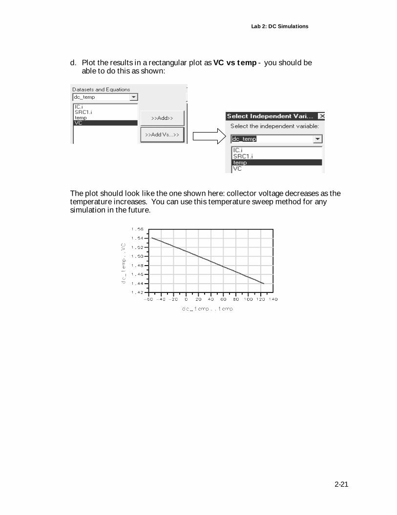
d. Plot the results in a rectangular plot as VC vs temp - you should beable to do this as shown:
The plot should look like the one shown here: collector voltage decreases as thetemperature increases. You can use this temperature sweep method for anysimulation in the future.
Lab 2: DC Simulations
2-22
EXTRA EXERCISES
1. Plot current (probe) vs. temperature.
2. Try these commands:
a. Select the bjt and click the command: Edit > Component > BreakConnections. Reinsert the bjt and see what happens.
b. Spend a few moments experimenting with the other Simulation menucommands: Highlight Node and Detailed Device Operating Point. Theseare only available after a dc simulation.
c. Go to the data display: Use the right mouse button and experimentwith the selections.
2. Replace the Gummel-Poon model card with another model (Mextram) andresimulate. Afterward, compare the results.