Embed Size (px)
Citation preview

Lab 5: PCB Design with Altium EECS 473
1
On the website is an Altium tutorial. Do it.
1. Pre-Lab_____________________
Q1. Once you’ve finished the tutorial, get a screenshot
of your board design. It should look similar to the
figure to the right.
Q2. Do the following tutorials which cover how to
create a device (a package and symbol combined together is a device)
https://www.altium.com/documentation/18.0/display/ADES/((A+Look+at+Creating+Library+Component s))_AD
Complete the sections on the webpage in the following order:
Creating a New Library Package and Schematic Library
Creating a New Schematic Component
Adding Pins to the Schematic Component
Setting the Schematic Component’s Properties
Creating PCB Component Footprints
Creating A New PCB Library
Manually Creating a Footprint
Adding Footprint Models to a Schematic Component
Checking the Component and Generating Reports
After completing the sections above, provide screen captures of your completed device. It should look something like this:
Lab 5: PCB Design with Altium EECS 473
2
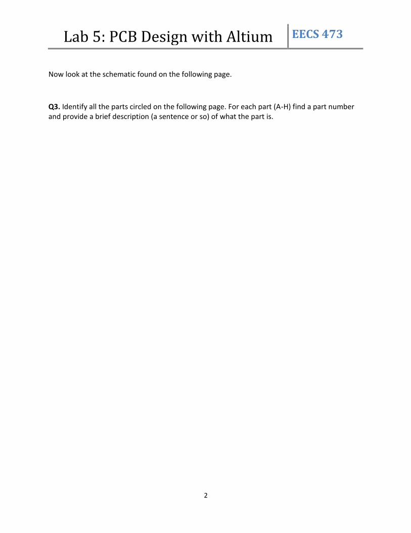
Now look at the schematic found on the following page.
Q3. Identify all the parts circled on the following page. For each part (A-H) find a part number and provide a brief description (a sentence or so) of what the part is.
Lab 5: PCB Design with Altium EECS 473
3
Lab 5: PCB Design with Altium EECS 473
4
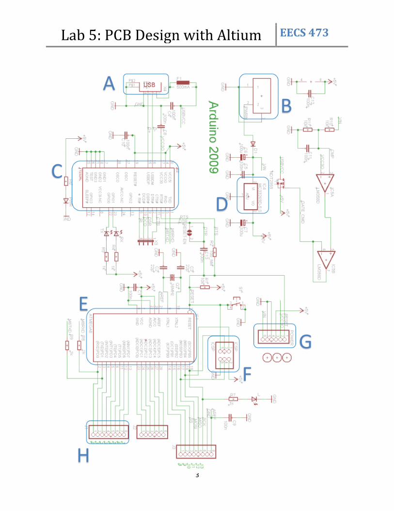
2. In-Lab_____________________________________________
Note: The in-lab is based heavily on the Lab 5: PCB Design with EAGLE, which is based on the EAGLE lessons from the Michigan Embedded Systems Hub.
Lab 5: PCB Design with Altium EECS 473
5
Introduction__________________________________________
In the prelab, you gained experience performing schematic capture and board layout with a simple board in Altium and looked at a much larger design. In this section, we will be exploring a mid-sized board featuring a simple microcontroller-based system, including a power supply and supporting components such as LEDs.
Part 1: Setting up Altium________________________________
The first thing we need to do is setup Altium. Go to the labs site and download the lab5.zip file and extract the LAB5_files folder. We will be using the EAGLE MESH library within Altium, so we will need to import the files.
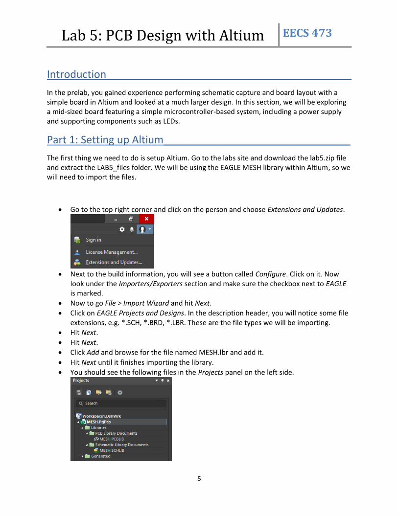
Go to the top right corner and click on the person and choose Extensions and Updates.
Next to the build information, you will see a button called Configure. Click on it. Now
look under the Importers/Exporters section and make sure the checkbox next to EAGLE is marked.
Now to go File > Import Wizard and hit Next.
Click on EAGLE Projects and Designs. In the description header, you will notice some file extensions, e.g. *.SCH, *.BRD, *.LBR. These are the file types we will be importing.
Hit Next.
Hit Next.
Click Add and browse for the file named MESH.lbr and add it.
Hit Next until it finishes importing the library.
You should see the following files in the Projects panel on the left side.

Lab 5: PCB Design with Altium EECS 473
6
We have now successfully imported the EAGLE MESH library into Altium. We can now start creating our schematic.
Part 2: Creating a New Schematic_________________________
Create a schematic by going to File > New > Schematic.
The core components of a design are those that will affect the functionality. In our simple example project, the core components are the voltage regulator and the processor (MCU). We will design those now.
2.1 Power Supply
2.1.1 Place Part
We will start our design by adding our linear dropout regulator (LDO) and the support components that it requires. First, let’s check to make sure that our MESH library is properly installed and that we are able to search parts from it.
Click on Panels in the bottom right corner and click on Libraries.
You will see a panel pop up on the right side. Click on Libraries near the top.
Go to the Installed tab and check that the MESH.IntLib is activated. Close the box.

Lab 5: PCB Design with Altium EECS 473
7
Now that we have ensured the MESH library is activated, we can search for the regulator.
In the Libraries panel, click on Search near the top.
Set the Field to Name, Operator to contains, and Value to LM340.
In the Scope section, click on the radio button next to Available libraries.
Hit Search.
You should now see at least 1 component in the Libraries panel on the right side.
We want the LM340MPX-5.0/NOPB from the MESH.SCHLIB.
Double click on the component, or right click and hit Place.
Add the part somewhere on the schematic sheet by left clicking. Hit escape to prevent placing the part multiple times.
2.1.2 Add Capacitors
Most voltage regulators will require some capacitors to function. Information on how many capacitors and of what size are required can be found in the voltage regulator’s datasheet. Let’s take a look at the LM340MPX-5.0 datasheet. The datasheet is included in the Lab5_files you downloaded from the lab site.
On the first page, find Figure 1 – “Fixed Output Regulation”.
As we can see, we require one 220nF capacitor and one 100nF ceramic capacitor. For more information on using capacitors in power supplies including capacitor type and ESR, ask your instructor or refer to the lecture presentation available online.
Lab 5: PCB Design with Altium EECS 473
8
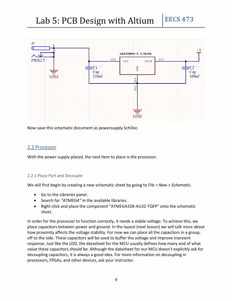
We will add the ceramic caps first.
Go back to the Libraries panel and hit Search.
Make sure the Operator is contains. Search Cap in Available Libraries.
You should now see a few components in the Libraries panel.
Right click on Cap and place this part twice within the schematic sheet on either side of the regulator.
You can rotate the capacitor before placing by hitting the Space key.
After placing the capacitors, right click on the ‘220nF’ text next to the left capacitor and select Properties.
Change the Value to ‘220nF’.
Do the same for the other capacitor, setting its Value to ‘100nF’.
Double click on “C?” next to each capacitor and change the Values to C1 and C2 for the left and right capacitors, respectively.
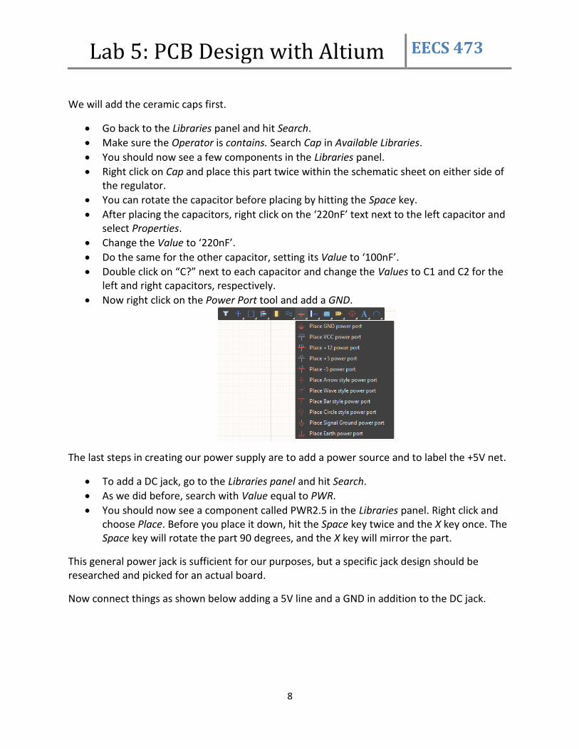
Now right click on the Power Port tool and add a GND.
The last steps in creating our power supply are to add a power source and to label the +5V net.
To add a DC jack, go to the Libraries panel and hit Search.
As we did before, search with Value equal to PWR.
You should now see a component called PWR2.5 in the Libraries panel. Right click and choose Place. Before you place it down, hit the Space key twice and the X key once. The Space key will rotate the part 90 degrees, and the X key will mirror the part.
This general power jack is sufficient for our purposes, but a specific jack design should be researched and picked for an actual board.
Now connect things as shown below adding a 5V line and a GND in addition to the DC jack.
Lab 5: PCB Design with Altium EECS 473
9
Now save this schematic document as powersupply.SchDoc.
2.2 Processor
With the power supply placed, the next item to place is the processor.
2.2.1 Place Part and Decouple
We will first begin by creating a new schematic sheet by going to File > New > Schematic.
Go to the Libraries panel.
Search for “ATMEGA” in the available libraries.
Right click and place the component “ATMEGA328-AU32-TQFP” onto the schematic sheet.
In order for the processor to function correctly, it needs a stable voltage. To achieve this, we place capacitors between power and ground. In the layout (next lesson) we will talk more about how proximity affects the voltage stability. For now we can place all the capacitors in a group, off to the side. These capacitors will be used to buffer the voltage and improve transient response. Just like the LDO, the datasheet for the MCU usually defines how many and of what value these capacitors should be. Although the datasheet for our MCU doesn’t explicitly ask for decoupling capacitors, it is always a good idea. For more information on decoupling in processors, FPGAs, and other devices, ask your instructor.
Lab 5: PCB Design with Altium EECS 473
10
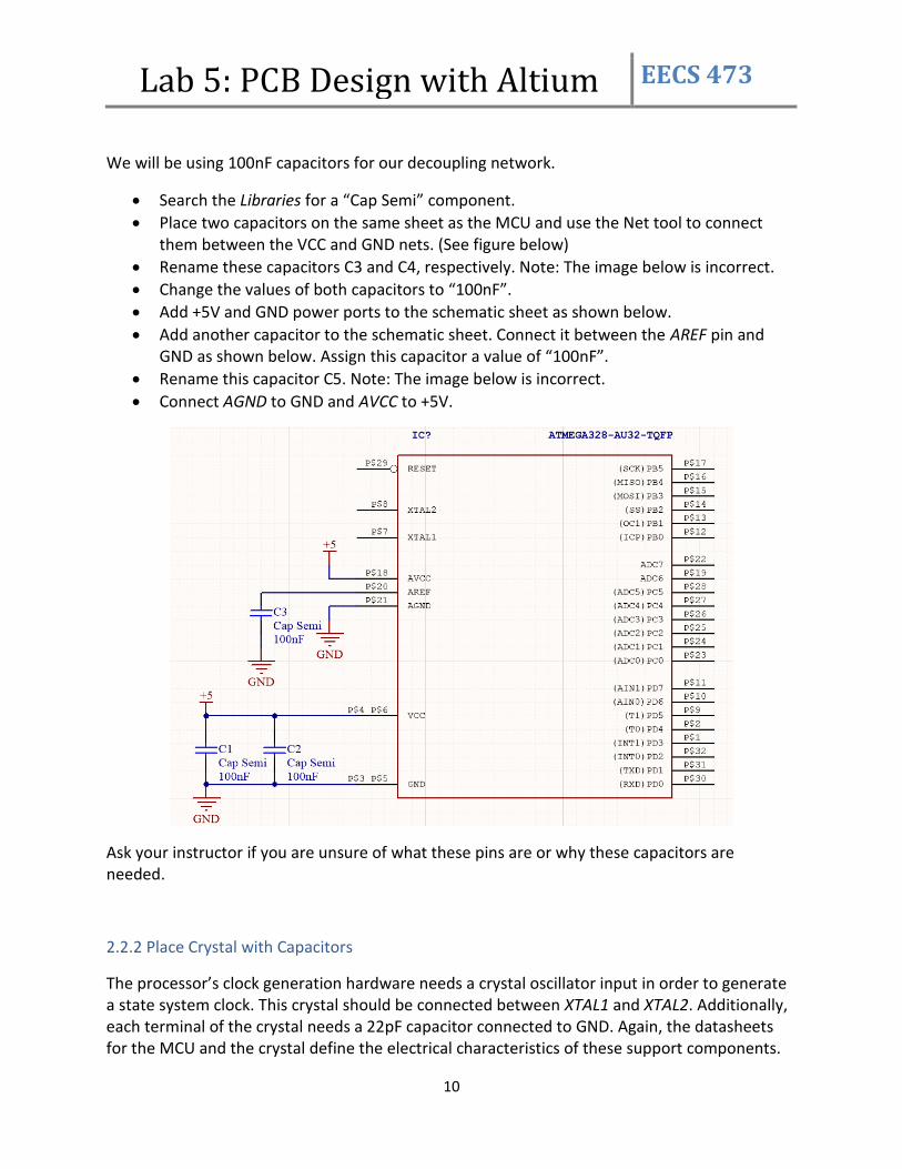
We will be using 100nF capacitors for our decoupling network.
Search the Libraries for a “Cap Semi” component.
Place two capacitors on the same sheet as the MCU and use the Net tool to connect them between the VCC and GND nets. (See figure below)
Rename these capacitors C3 and C4, respectively. Note: The image below is incorrect.
Change the values of both capacitors to “100nF”.
Add +5V and GND power ports to the schematic sheet as shown below.
Add another capacitor to the schematic sheet. Connect it between the AREF pin and GND as shown below. Assign this capacitor a value of “100nF”.
Rename this capacitor C5. Note: The image below is incorrect.
Connect AGND to GND and AVCC to +5V.
Ask your instructor if you are unsure of what these pins are or why these capacitors are needed.
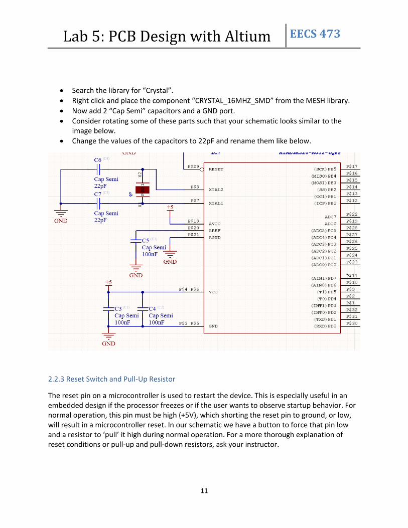
2.2.2 Place Crystal with Capacitors
The processor’s clock generation hardware needs a crystal oscillator input in order to generate a state system clock. This crystal should be connected between XTAL1 and XTAL2. Additionally, each terminal of the crystal needs a 22pF capacitor connected to GND. Again, the datasheets for the MCU and the crystal define the electrical characteristics of these support components.
Lab 5: PCB Design with Altium EECS 473
11
Search the library for “Crystal”.
Right click and place the component “CRYSTAL_16MHZ_SMD” from the MESH library.
Now add 2 “Cap Semi” capacitors and a GND port.
Consider rotating some of these parts such that your schematic looks similar to the image below.
Change the values of the capacitors to 22pF and rename them like below.
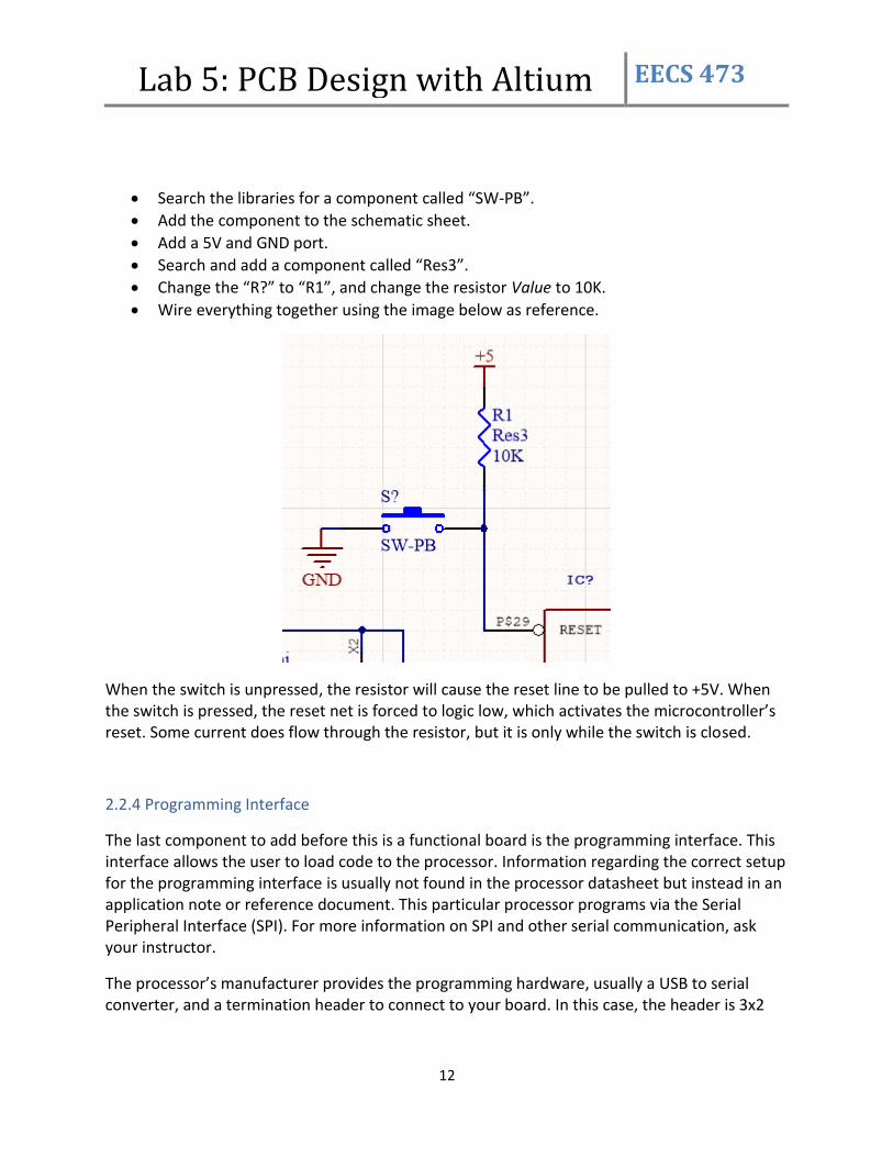
2.2.3 Reset Switch and Pull-Up Resistor
The reset pin on a microcontroller is used to restart the device. This is especially useful in an embedded design if the processor freezes or if the user wants to observe startup behavior. For normal operation, this pin must be high (+5V), which shorting the reset pin to ground, or low, will result in a microcontroller reset. In our schematic we have a button to force that pin low and a resistor to ‘pull’ it high during normal operation. For a more thorough explanation of reset conditions or pull-up and pull-down resistors, ask your instructor.
Lab 5: PCB Design with Altium EECS 473
12
Search the libraries for a component called “SW-PB”.
Add the component to the schematic sheet.
Add a 5V and GND port.
Search and add a component called “Res3”.
Change the “R?” to “R1”, and change the resistor Value to 10K.
Wire everything together using the image below as reference.
When the switch is unpressed, the resistor will cause the reset line to be pulled to +5V. When the switch is pressed, the reset net is forced to logic low, which activates the microcontroller’s reset. Some current does flow through the resistor, but it is only while the switch is closed.
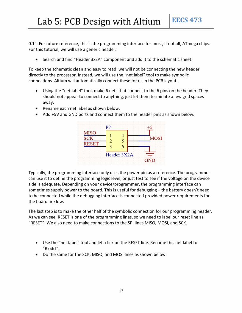
2.2.4 Programming Interface
The last component to add before this is a functional board is the programming interface. This interface allows the user to load code to the processor. Information regarding the correct setup for the programming interface is usually not found in the processor datasheet but instead in an application note or reference document. This particular processor programs via the Serial Peripheral Interface (SPI). For more information on SPI and other serial communication, ask your instructor.
The processor’s manufacturer provides the programming hardware, usually a USB to serial converter, and a termination header to connect to your board. In this case, the header is 3x2
Lab 5: PCB Design with Altium EECS 473
13
0.1”. For future reference, this is the programming interface for most, if not all, ATmega chips. For this tutorial, we will use a generic header.
Search and find “Header 3x2A” component and add it to the schematic sheet.
To keep the schematic clean and easy to read, we will not be connecting the new header directly to the processor. Instead, we will use the “net label” tool to make symbolic connections. Altium will automatically connect these for us in the PCB layout.
Using the “net label” tool, make 6 nets that connect to the 6 pins on the header. They should not appear to connect to anything, just let them terminate a few grid spaces away.
Rename each net label as shown below.
Add +5V and GND ports and connect them to the header pins as shown below.
Typically, the programming interface only uses the power pin as a reference. The programmer can use it to define the programming logic level, or just test to see if the voltage on the device side is adequate. Depending on your device/programmer, the programming interface can sometimes supply power to the board. This is useful for debugging – the battery doesn’t need to be connected while the debugging interface is connected provided power requirements for the board are low.
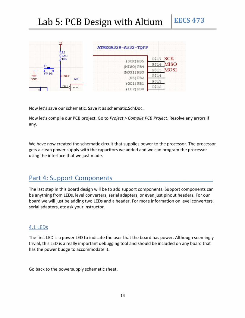
The last step is to make the other half of the symbolic connection for our programming header. As we can see, RESET is one of the programming lines, so we need to label our reset line as “RESET”. We also need to make connections to the SPI lines MISO, MOSI, and SCK.
Use the “net label” tool and left click on the RESET line. Rename this net label to “RESET”.
Do the same for the SCK, MISO, and MOSI lines as shown below.
Lab 5: PCB Design with Altium EECS 473
14
Now let’s save our schematic. Save it as schematic.SchDoc.
Now let’s compile our PCB project. Go to Project > Compile PCB Project. Resolve any errors if any.
We have now created the schematic circuit that supplies power to the processor. The processor gets a clean power supply with the capacitors we added and we can program the processor using the interface that we just made.
Part 4: Support Components____________________________
The last step in this board design will be to add support components. Support components can be anything from LEDs, level converters, serial adapters, or even just pinout headers. For our board we will just be adding two LEDs and a header. For more information on level converters, serial adapters, etc ask your instructor.
4.1 LEDs
The first LED is a power LED to indicate the user that the board has power. Although seemingly trivial, this LED is a really important debugging tool and should be included on any board that has the power budge to accommodate it.
Go back to the powersupply schematic sheet.
Lab 5: PCB Design with Altium EECS 473
15
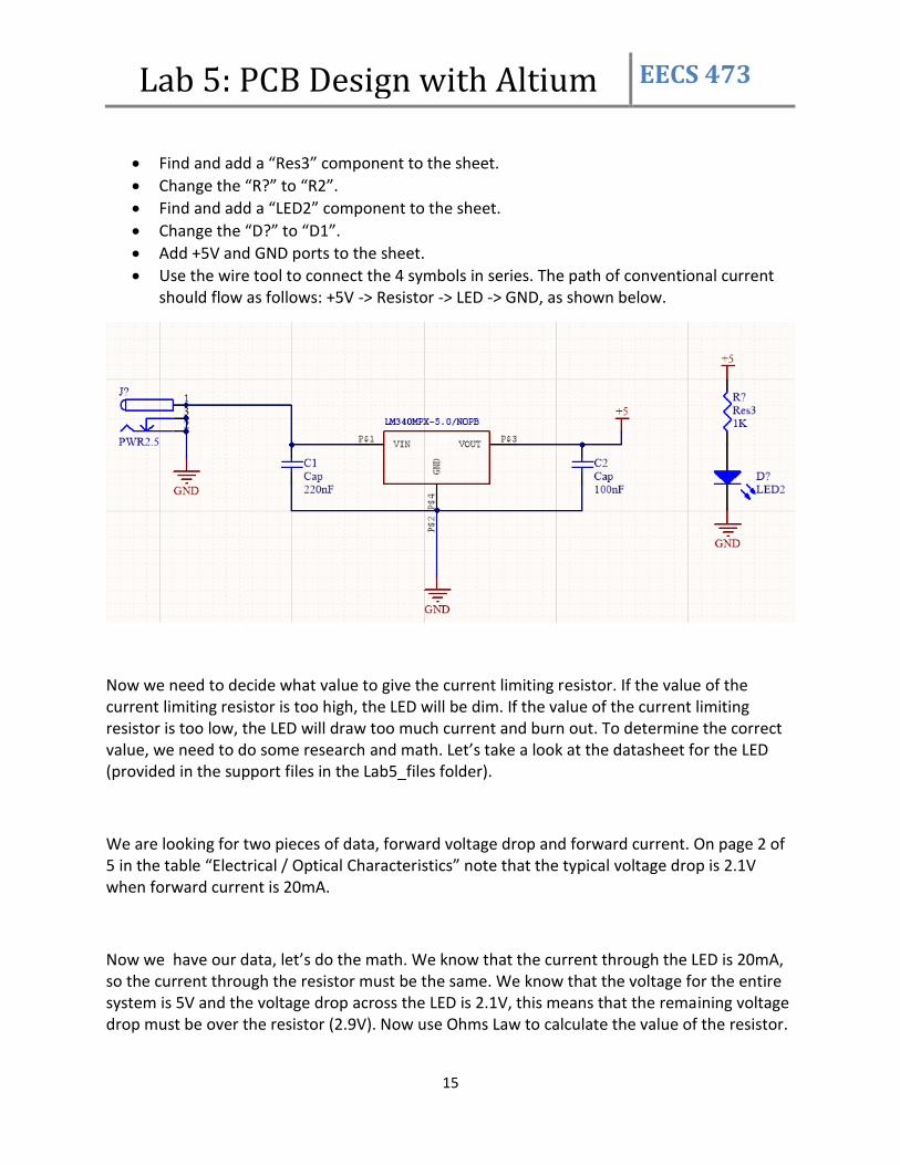
Find and add a “Res3” component to the sheet.
Change the “R?” to “R2”.
Find and add a “LED2” component to the sheet.
Change the “D?” to “D1”.
Add +5V and GND ports to the sheet.
Use the wire tool to connect the 4 symbols in series. The path of conventional current should flow as follows: +5V -> Resistor -> LED -> GND, as shown below.
Now we need to decide what value to give the current limiting resistor. If the value of the current limiting resistor is too high, the LED will be dim. If the value of the current limiting resistor is too low, the LED will draw too much current and burn out. To determine the correct value, we need to do some research and math. Let’s take a look at the datasheet for the LED (provided in the support files in the Lab5_files folder).
We are looking for two pieces of data, forward voltage drop and forward current. On page 2 of 5 in the table “Electrical / Optical Characteristics” note that the typical voltage drop is 2.1V when forward current is 20mA.
Now we have our data, let’s do the math. We know that the current through the LED is 20mA, so the current through the resistor must be the same. We know that the voltage for the entire system is 5V and the voltage drop across the LED is 2.1V, this means that the remaining voltage drop must be over the resistor (2.9V). Now use Ohms Law to calculate the value of the resistor.

Lab 5: PCB Design with Altium EECS 473
16
V = I*R, or rearranged, R = V/I = 2.9 / 0.02 = 145 Ohms. 145 Ohms is not a standard resistor value, so we round up to the nearest standard value (150 Ohms).
Another aspect to consider is the power dissipated by the current limiting resistor. Recall that Power = V*I. Our resistor will be dissipating 2.9 * 0.02 = 0.058 Watts. Typical 0603 resistors are 0.1 W rated, so this design will work. If we wanted a smaller resistor (with lower power rating) or higher current (brighter LED), then we would have to choose components that match specifications. For more information about choosing components, current limiting resistors, or LED circuit design, ask your instructor.
Give the “Res3” resistor a value of 150.
The next LED that we place will be a debugging LED connected to one of the digital IO pins of the processor. The user will then be able to toggle this LED through software. We are going to place our LED on the SCK line. This line is used during programming and then becomes user I/O. An LED on SCK, therefore, will indicate to the user that programming is happening and then become available for other use.
Switch back to the schematic with the processor.
Add the same “Res3” and “LED2” components to the sheet.
Change the “R?” to “R3”, and the “D?” to “D2”.
Instead of using the +5V power port as we did earlier, we will use the SCK line as the high voltage. Use a GND port as well did before.
Give the resistor a value of 150.
Give the LED a value of RED.
Note that the LED will be illuminated when SCK is high and off when SCK is low. The datasheet for the MCU defines the “Absolute Maximum Rating” for each I/O pin to be 40mA. The 20mA draw of the LED is well within this limit.
Lab 5: PCB Design with Altium EECS 473
17
4.2 Headers
Because this board is essentially a platform for numerous different applications, it is likely that various processor IO pins will be needed in the future. The pins on the processor itself are far too tiny to solder directly to so we will provide a header to make this easier. If you are unsure of what a header is, ask your instructor.
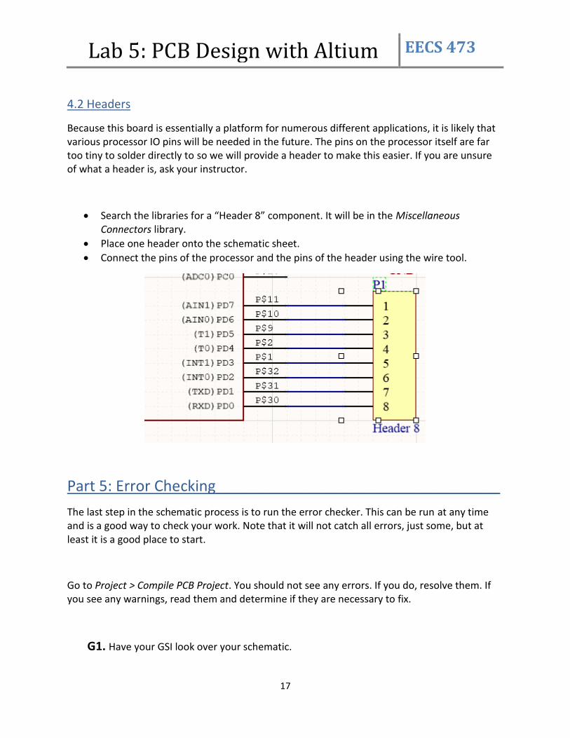
Search the libraries for a “Header 8” component. It will be in the Miscellaneous Connectors library.
Place one header onto the schematic sheet.
Connect the pins of the processor and the pins of the header using the wire tool.
Part 5: Error Checking__________________________________
The last step in the schematic process is to run the error checker. This can be run at any time and is a good way to check your work. Note that it will not catch all errors, just some, but at least it is a good place to start.
Go to Project > Compile PCB Project. You should not see any errors. If you do, resolve them. If you see any warnings, read them and determine if they are necessary to fix.
G1. Have your GSI look over your schematic.
Lab 5: PCB Design with Altium EECS 473
18
Part 6: Initialize and Outline Board________________________
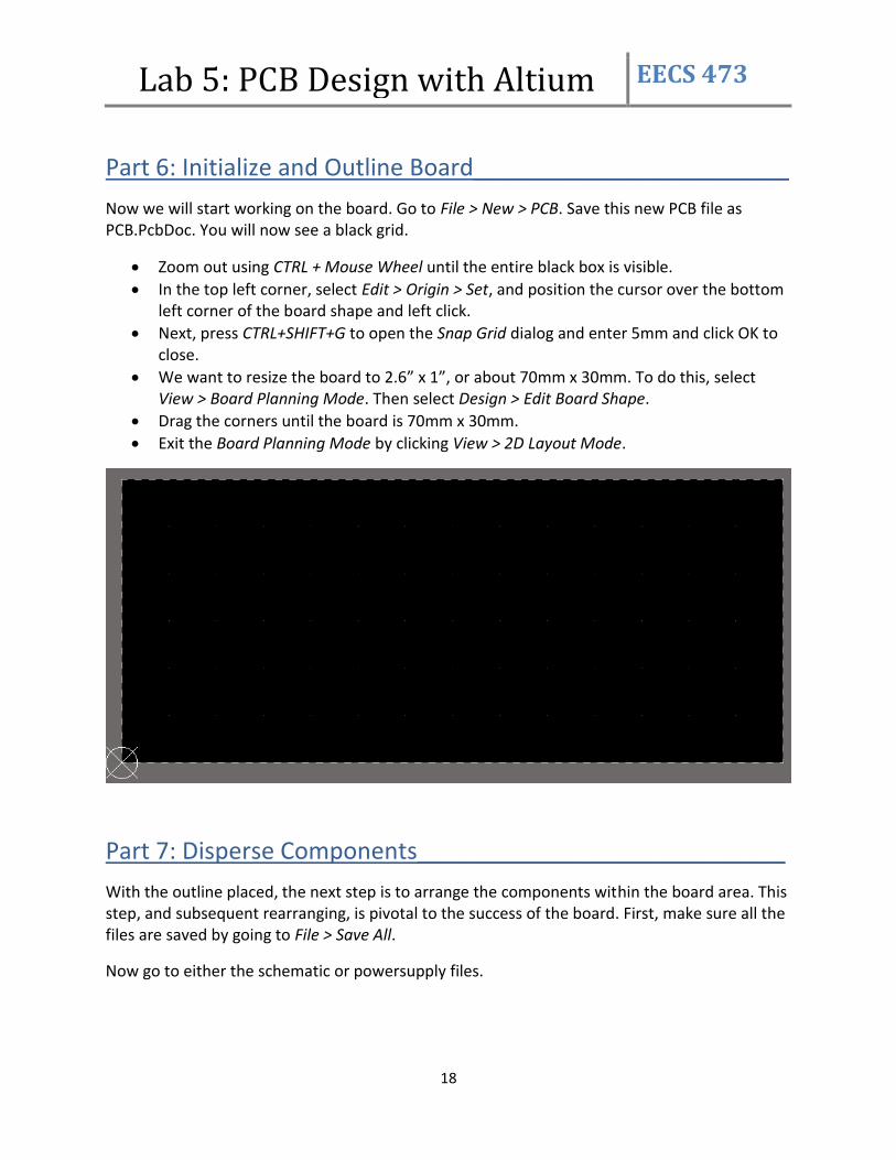
Now we will start working on the board. Go to File > New > PCB. Save this new PCB file as PCB.PcbDoc. You will now see a black grid.
Zoom out using CTRL + Mouse Wheel until the entire black box is visible.
In the top left corner, select Edit > Origin > Set, and position the cursor over the bottom left corner of the board shape and left click.
Next, press CTRL+SHIFT+G to open the Snap Grid dialog and enter 5mm and click OK to close.
We want to resize the board to 2.6” x 1”, or about 70mm x 30mm. To do this, select View > Board Planning Mode. Then select Design > Edit Board Shape.
Drag the corners until the board is 70mm x 30mm.
Exit the Board Planning Mode by clicking View > 2D Layout Mode.
Part 7: Disperse Components____________________________
With the outline placed, the next step is to arrange the components within the board area. This step, and subsequent rearranging, is pivotal to the success of the board. First, make sure all the files are saved by going to File > Save All.
Now go to either the schematic or powersupply files.

Lab 5: PCB Design with Altium EECS 473
19
Go to Design > Update PCB Document.
You will see a box like this:
Click on Validate Changes. If everything goes smoothly, you will see a green check mark
next to every component.
Now click on Execute Changes. This will import all our components into the PCB file. You should now see this within the PCB.PcbDoc file:
You can click on the red boxes and hit the Delete key.
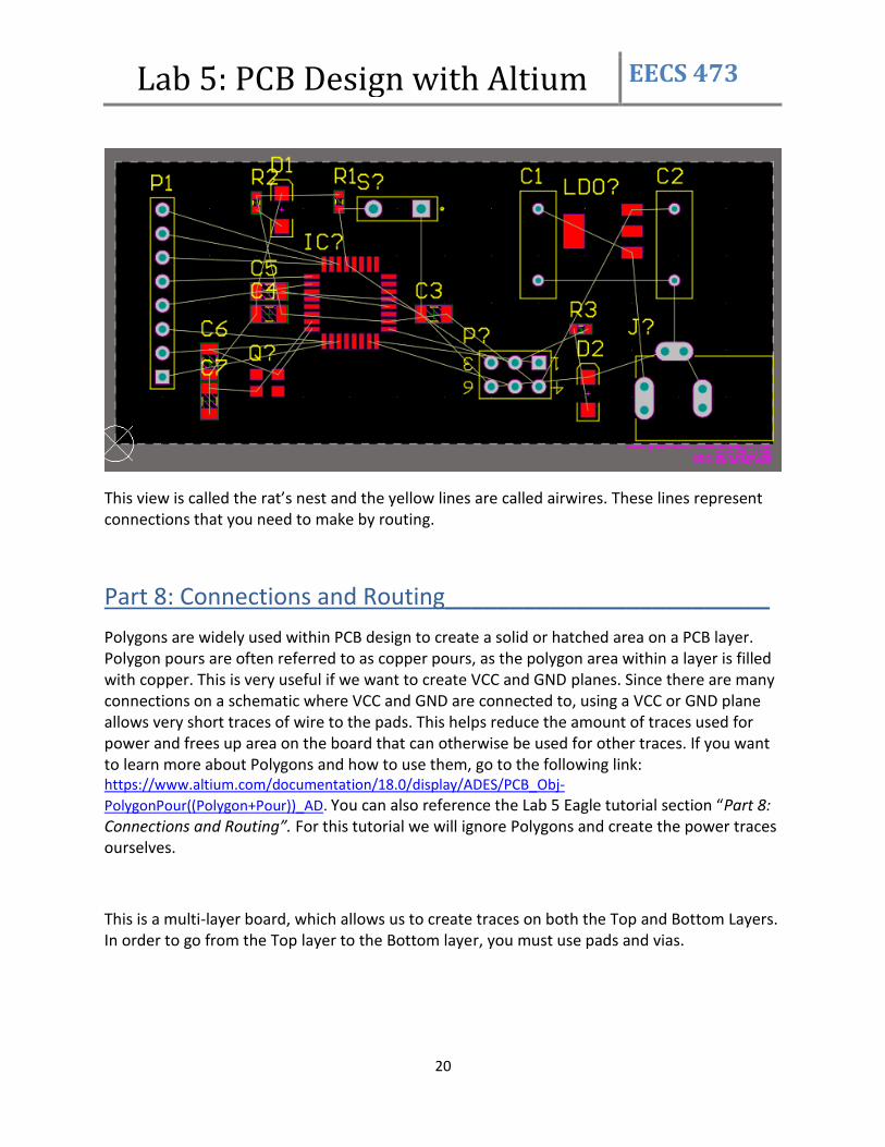
Rearrange and place the components onto the PCB grid. Start with the regulator, “LDO?”, and the processor, “IC?”. Group these items separately and with enough space for support components. Make sure that the decoupling capacitors for the microprocessor and voltage regulator are as close to the ICs as possible. Place the connectors, headers, and switch last.
Lab 5: PCB Design with Altium EECS 473
20
This view is called the rat’s nest and the yellow lines are called airwires. These lines represent connections that you need to make by routing.
Part 8: Connections and Routing_________________________
Polygons are widely used within PCB design to create a solid or hatched area on a PCB layer. Polygon pours are often referred to as copper pours, as the polygon area within a layer is filled with copper. This is very useful if we want to create VCC and GND planes. Since there are many connections on a schematic where VCC and GND are connected to, using a VCC or GND plane allows very short traces of wire to the pads. This helps reduce the amount of traces used for power and frees up area on the board that can otherwise be used for other traces. If you want to learn more about Polygons and how to use them, go to the following link: https://www.altium.com/documentation/18.0/display/ADES/PCB_Obj-
PolygonPour((Polygon+Pour))_AD. You can also reference the Lab 5 Eagle tutorial section “Part 8: Connections and Routing”. For this tutorial we will ignore Polygons and create the power traces ourselves.
This is a multi-layer board, which allows us to create traces on both the Top and Bottom Layers. In order to go from the Top layer to the Bottom layer, you must use pads and vias.
Lab 5: PCB Design with Altium EECS 473
21
As we learned in the Altium tutorial from the Pre-Lab, you can choose between Interactive Routing and Active Routing. Interactive Routing involves manually wiring the traces together. This method allows for more control over the board design, as you can route traces to be efficient and clean. Active Routing involves automatically connecting some or all of the traces together. This is helpful for beginners, since Altium will create the traces optimally and very quickly. However, the Active Routing tool is not perfect, and does not always create the traces in the most efficient manner. If you do use the Active Routing tool, you may end up with a few air wires that you will need to manually wire.
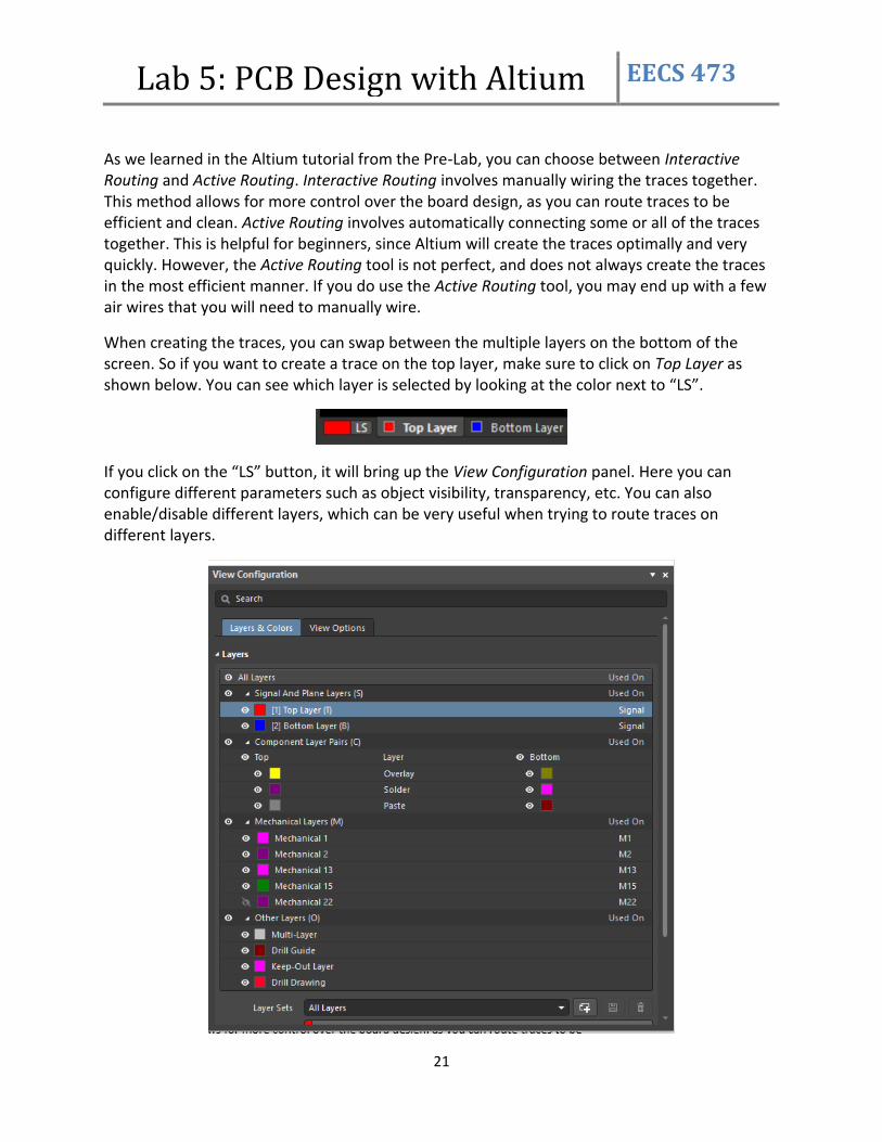
When creating the traces, you can swap between the multiple layers on the bottom of the screen. So if you want to create a trace on the top layer, make sure to click on Top Layer as shown below. You can see which layer is selected by looking at the color next to “LS”.
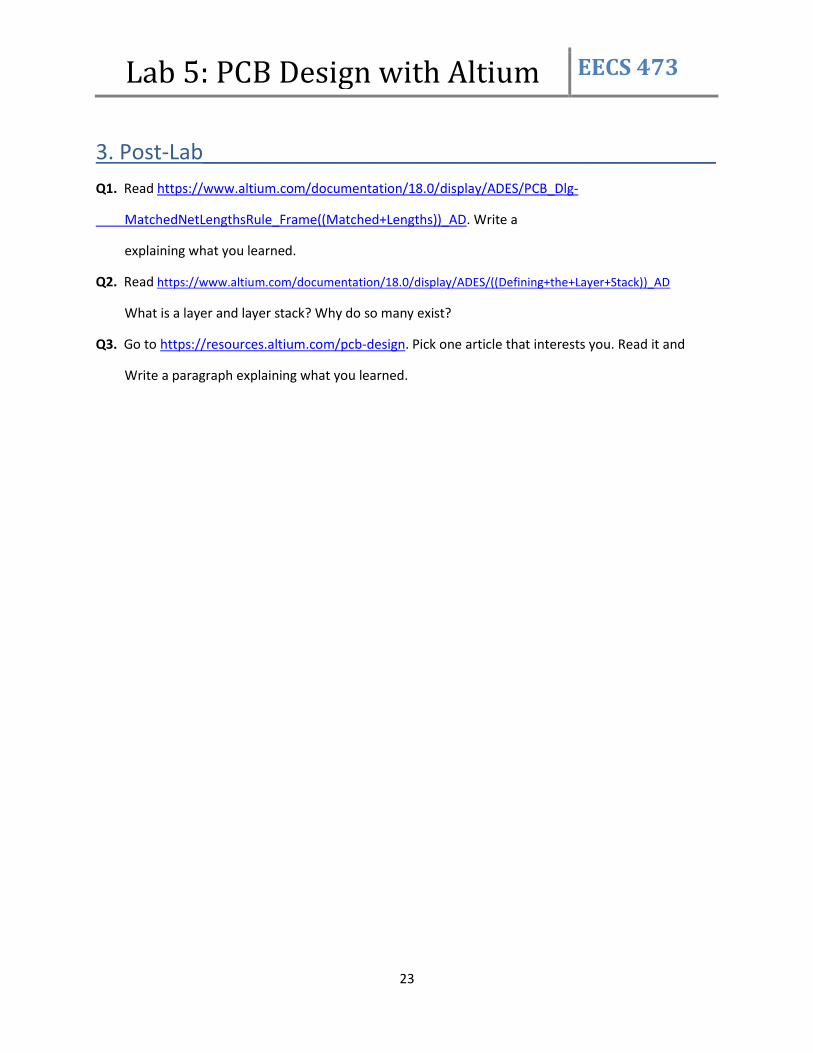
If you click on the “LS” button, it will bring up the View Configuration panel. Here you can configure different parameters such as object visibility, transparency, etc. You can also enable/disable different layers, which can be very useful when trying to route traces on different layers.

Lab 5: PCB Design with Altium EECS 473
22
After routing everything together, we will compile and error check.
Go to Project > Compile PCB Project and resolve any errors.
Go to Tools > Design Rule Check and click on Run Design Rule Check. Resolve any errors that pop up.
If everything goes well, you should now have a complete board design.
Part 9: Gerber Files____________________________________
Now that our board design is complete, we are ready to generate the files needed to send our PCB to a fabrication house.
Go to File > Fabrication Outputs > Gerber Files.
On the General tab, choose Millimeters as the units.
On the General tab, choose 4:3 as the format.
On the Layers tab, click Plot Layers and select Used On.
On the Layers tab, disable any mechanical layers.
On the Advanced tab, confirm that the Position on Film is set to Reference to relative origin.
Click OK. Save this file.
G2. Show your board layout to your GSI. Be able to justify the decisions you’ve made.
G3. Create a zipfile of your Gerber files and drill hole file you’d need for the manufacture of
your board. Show your GSI.
Lab 5: PCB Design with Altium EECS 473
23
3. Post-Lab___________________________________________
Q1. Read https://www.altium.com/documentation/18.0/display/ADES/PCB_Dlg-
MatchedNetLengthsRule_Frame((Matched+Lengths))_AD. Write a
explaining what you learned.
Q2. Read https://www.altium.com/documentation/18.0/display/ADES/((Defining+the+Layer+Stack))_AD
What is a layer and layer stack? Why do so many exist?
Q3. Go to https://resources.altium.com/pcb-design. Pick one article that interests you. Read it and
Write a paragraph explaining what you learned.


![EECS 473 Midterm Exam - University of Michigan 473 Midterm Exam Fall 2017 ... T3 Period % Utilization A 2 10 3 9 4 8 103.3% ... Design Question [31 points]](https://img.pdfslide.net/doc/110x75/5ab90e747f8b9ad5338d8bec/eecs-473-midterm-exam-university-of-michigan-473-midterm-exam-fall-2017-t3.jpg)