Embed Size (px)
DESCRIPTION
LAB REPORT 012
Citation preview
7/17/2019 Lab Report 04
http://slidepdf.com/reader/full/lab-report-04-568cb00c86304 1/4
Lab Report # 04
To construct a Common Emitter amplifier and calculate
its voltage gain with & without feedback
Theory:
A common emitter is a type of electronic amplifier stage based on
a bipolar transistor in series with a load element such as a resistor. The
term "common emitter" refers to the fact that the emitter node of the
transistor indicated by an arrow symbol! is connected to a "common" power
rail typically the # volt reference or ground node. The collector node is
connected to the output load and the base node acts as input.
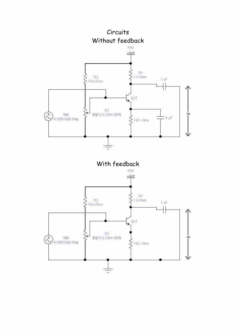
Explanation of circuit:
The electronic circuit diagram given below shows
a common emitter configuration with voltage divider bias CE$%!. 'n the
figure the common emitter circuit comprises the load resistor (C and )*)
transistor with the output connected as shown+ the other circuit elements
are used for biasing the transistor and signal coupling,decoupling.
The resistor (E between the emitter node and the shared ground appears at
first glance to contradict the strict definition of "common emitter" but the
term is still appropriate here because for all fre-uencies of interest the
capacitor CE acts as low impedance by decoupling the emitter to ground. The
emitter resistor provides a form of negative feedback called emitter
degeneration which increases the stability and linearity of the amplifier
especially in response to temperature changes.
or the common emitter circuit on the right this is necessary to ensure the
transistor is in the active mode and thus prevent it from acting as a
rectifier which would cause clipping on the negative portion of the input
signal resulting in a distorted output.
7/17/2019 Lab Report 04
http://slidepdf.com/reader/full/lab-report-04-568cb00c86304 2/4
The resistors (/ and (0 are chosen to ensure the base1emitter voltage is
appro2imately #.3 volts which is the "on" voltage for a 4T transistor.
These resistors along with (E also determine the -uiescent current flowing
through the transistor and therefore its gain.
eedback concept:
'f some percentage of an amplifier5s output signal is
connected to the input so that the amplifier amplifies part of its own output
signal we have what is known as feedback . eedback comes in two varieties:
positive also called regenerative ! and negative also called degenerative !.
*ositive feedback reinforces the direction of an amplifier5s output voltagechange.
)egative feedback on the other hand has a "dampening" effect on an
amplifier: if the output signal happens to increase in magnitude the
feedback signal introduces a decreasing influence into the input of the
amplifier thus opposing the change in output signal. 6hile positive feedback
drives an amplifier circuit toward a point of instability oscillations!
negative feedback drives it the opposite direction: toward a point of
stability.
An amplifier circuit e-uipped with some amount of negative feedback
is not only more stable but it tends to distort the input waveform to a
lesser degree and is generally capable of amplifying a wider range of
fre-uencies. The tradeoff for these advantages there 7ust has to be a
disadvantage to negative feedback right8! is decreased gain. 'f a portion of
an amplifier5s output signal is "fed back" to the input in such a way as to
oppose any changes in the output it will re-uire a greater input signal
amplitude to drive the amplifier5s output to the same amplitude as before.
This constitutes a decreased gain. 9owever the advantages of stabilitylower distortion and greater bandwidth are worth the tradeoff in reduced
gain for many applications.
7/17/2019 Lab Report 04
http://slidepdf.com/reader/full/lab-report-04-568cb00c86304 3/4
Circuits
6ithout feedback
6ith feedback

7/17/2019 Lab Report 04
http://slidepdf.com/reader/full/lab-report-04-568cb00c86304 4/4
*rocedure: The circuit was set up as shown in the circuit diagram. The
/; resistor was connected to Collector. The emitter terminal was
connected to /##; resistor and on its way to the ground which provides a
feedback path to input. Two additional resistances of /#; were inserted
between the base terminals to produce the voltage divider bias. The
coupling capacitors were inserted as well to ensure the ma2imum gain. To
measure the output & input voltages $in & $out! an oscilloscope was connected
across the transistor the readings were reconfirmed using voltmeter
.inally after taking all precautions into account ' got up the readings and
calculated the voltage gain Av!.
The readings are plotted in the observation chart below:
<bservations & Calculations
$CC $! $') $! $<=T $! with
f,b
$<=T $!without f,b
A$ with
f,b
A$ without
f,b
/> /0m$ #./0 #.?/ 1/# 1@3.>
/> /#m$ #.#@@ #.? 1@.@ 1?/> #?m$ #.#@ #.@ 1? 1>3.>
/> 14mV 0.13 0.91 -9.2 -65
Applications:
Common emitter circuits are used to amplify weak voltagesignals such as the faint radio signals detected by an antenna. They are also
used in a special analog circuit configuration known as a current mirror
where a single shared input is used to drive a set of identical transistors
each of whose current drive output will be nearly identical to each other
even if they are driving dissimilar output loads.


![[LAB]04 TeoriaQuadradosMinimos](https://img.pdfslide.net/doc/110x75/55cf9bd6550346d033a78f0b/lab04-teoriaquadradosminimos.jpg)