Embed Size (px)
Citation preview
Large-Scale Synthesis of High-Quality Hexagonal Boron NitrideNanosheets for Large-Area Graphene ElectronicsKang Hyuck Lee,†,|| Hyeon-Jin Shin,‡,|| Jinyeong Lee,† In-yeal Lee,§ Gil-Ho Kim,§ Jae-Young Choi,*,‡
and Sang-Woo Kim*,†
†School of Advanced Materials Science and Engineering, SKKU Advanced Institute of Nanotechnology (SAINT), Center for HumanInterface Nanotechnology (HINT), SKKU-Samsung Graphene Center, Sungkyunkwan University (SKKU), Suwon 440-746,Republic of Korea‡Graphene Center, Samsung Advanced Institute of Technology, Yongin 446-712, Republic of Korea§SKKU Advanced Institute of Nanotechnology (SAINT), Department of Electronic and Electrical Engineering, SungkyunkwanUniversity (SKKU), Suwon 440-746, Republic of Korea
*S Supporting Information
ABSTRACT: Hexagonal boron nitride (h-BN) has received a greatdeal of attention as a substrate material for high-performancegraphene electronics because it has an atomically smooth surface,lattice constant similar to that of graphene, large optical phononmodes, and a large electrical band gap. Herein, we report the large-scale synthesis of high-quality h-BN nanosheets in a chemical vapordeposition (CVD) process by controlling the surface morphologiesof the copper (Cu) catalysts. It was found that morphology controlof the Cu foil is much critical for the formation of the pure h-BNnanosheets as well as the improvement of their crystallinity. For thefirst time, we demonstrate the performance enhancement of CVD-based graphene devices with large-scale h-BN nanosheets. Themobility of the graphene device on the h-BN nanosheets wasincreased 3 times compared to that without the h-BN nanosheets. The on−off ratio of the drain current is 2 times higher thanthat of the graphene device without h-BN. This work suggests that high-quality h-BN nanosheets based on CVD are verypromising for high-performance large-area graphene electronics.
KEYWORDS: Hexagonal boron nitride nanosheets, chemical vapor deposition, morphology control, large-scale synthesis,chemical polishing, graphene device
Hexagonal boron nitride (h-BN) is a layered material witha graphite-type structure in which planar networks of BN
hexagons are regularly stacked. h-BN with a wide band gap(∼5.9 eV)1 has many attractive properties for potentialapplications, for instance, high temperature stability, highmechanical strength, a large thermal conductivity, and a lowdielectric constant.2−6 Recently, h-BN has received a great dealof attention as a promising material substrate for high-qualitygraphene electronics because it has an atomically smoothsurface that is relatively free of dangling bonds and charge traps.It also has a similar lattice constant to graphene7 and shouldenable the tuning of its band gap.8 However, h-BN monolayersare generally produced by the micromechanical cleavage of abulk h-BN crystal, which is limited to small sizes and suitabletechniques.9,10 For practical applications, the realization ofhigh-quality and large-area h-BN consisting a homogeneousmonolayer or a few layers is essential.Recently, reproducible and scalable chemical vapor deposi-
tion (CVD) processes for fabricating few-layer h-BN films ontransition metal surfaces have been reported.11,12 Although
large-area few-layer h-BN films have been successfully realizedusing the CVD process, there are still many issues which remainto be resolved, including the formation of defects such asallotropes (amorphous BN (a-BN) and cubic BN (c-BN)) andthe generation of impurity particles with a heterostructure(BxCyNz/BN soot) on the h-BN surface. Thus, the achievementof large-scale high-quality h-BN layers with a low density ofdefects and impurity particles is strongly desirable to facilitatemore fundamental studies and industrial applications with two-dimensional layered nanomaterials.Herein, we demonstrate a facile method of growing large-
scale high-quality h-BN nanosheets by controlling the surfacemorphology of copper (Cu) foils acting as a catalyst. Thethermal annealing and chemical polishing of the Cu foil lead toan increase in its grain size and surface flatness. It was foundthat increasing the grain size and improving the flatness of the
Received: October 15, 2011Revised: December 15, 2011Published: January 5, 2012
Letter
pubs.acs.org/NanoLett
© 2012 American Chemical Society 714 dx.doi.org/10.1021/nl203635v | Nano Lett. 2012, 12, 714−718
surface of Cu result in the reduction in the amount of allotropes(c-BN) and impurity particles that are crucial for high-quality h-BN growth. Furthermore, we characterize for the first time theelectrical properties of large-scale CVD-grown graphene onCVD-grown h-BN nanosheets. A field effect transistor (FET)based on graphene was fabricated utilizing the large-scale h-BNnanosheets as a buffer layer on a SiO2 gate dielectric. Themobility and on/off ratio of the drain current (Ids) of the CVD-grown graphene FET with h-BN nanosheets grown on thethermally annealed and chemically polished Cu foil wereimproved by 3 and 2 times as compared to that of the CVD-grown graphene FET without the h-BN nanosheets,respectively. This implies that large-scale high-quality h-BNnanosheets should be useful for high-performance large-areagraphene electronics.The synthesis of h-BN layers was carried out in an ambient
pressure CVD system as described in a previous work.11 Forthe growth process, a Cu foil (Alpha Acer, 125 μm thickness)was placed in the CVD chamber and gradually heated up to1000 °C for 2 h 30 min in a mixed Ar/H2 (20 vol % H2, 80 vol% Ar) flow with a flow rate of 100 sccm. Then, the main growthwas carried out in a mixed Ar/H2 gas flow of 75 sccm for 30min at 1000 °C with ammonia borane (NH3−BH3) as thesource material sublimated at 110−130 °C using a subheatingchamber with an N2 gas flow of 25 sccm. It is known that such asublimation temperature leads to the formation of a hydro-borazine structure by cyclization.13 Finally, after the maingrowth, the chamber was cooled to 180 °C with a mixed Ar/H2gas flow at a flow rate of 100 sccm for 4 h. After the synthesis,the nanosheets were coated with poly(methyl methacrylate)(PMMA) and immersed in Cu etchant (Transene, type 1) inorder to etch away the Cu foil. When the Cu was completelyetched away, the h-BN nanosheets with PMMA were rinsed indeionized water several times to wash away the etchantresidues. Then, the PMMA-coated h-BN nanosheets weretransferred onto a SiO2 substrate for further characterizationand device fabrication.14,15
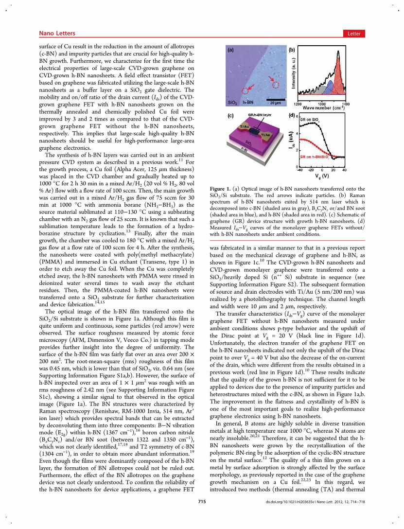
The optical image of the h-BN film transferred onto theSiO2/Si substrate is shown in Figure 1a. Although this film isquite uniform and continuous, some particles (red arrow) wereobserved. The surface roughness measured by atomic forcemicroscopy (AFM, Dimension V, Veeco Co.) in tapping modeprovides further insight into the degree of uniformity. Thesurface of the h-BN film was fairly flat over an area over 200 ×200 nm2. The root-mean-square (rms) roughness of this filmwas 0.45 nm, which is lower than that of SiO2, viz. 0.64 nm (seeSupporting Information Figure S1a,b). However, the surface ofh-BN inspected over an area of 1 × 1 μm2 was rough with anrms roughness of 2.42 nm (see Supporting Information FigureS1c), showing a similar signal to that observed in the opticalimage (Figure 1a). The BN structures were characterized byRaman spectroscopy (Renishaw, RM-1000 Invia, 514 nm, Ar+
ion laser) which provides spectral bands that can be extractedby deconvoluting them into three components: B−N vibrationmode (E2g) within h-BN (1367 cm−1),16 boron carbon nitride(BxCyNz) and/or BN soot (between 1322 and 1350 cm−1),which was not clearly identified,17,18 and T2 symmetry of c-BN(1304 cm−1), in order to obtain more abundant information.19
Even though the films were dominantly composed of the h-BNlayer, the formation of BN allotropes could not be ruled out.Furthermore, the effect of the BN allotropes on the graphenedevice was not clearly understood. To confirm the reliability ofthe h-BN nanosheets for device applications, a graphene FET
was fabricated in a similar manner to that in a previous reportbased on the mechanical cleavage of graphene and h-BN, asshown in Figure 1c.10 The CVD-grown h-BN nanosheets andCVD-grown monolayer graphene were transferred onto aSiO2/heavily doped Si (n++ Si) substrate in sequence (seeSupporting Information Figure S2). The subsequent formationof source and drain electrodes with Ti/Au (5 nm/200 nm) wasrealized by a photolithography technique. The channel lengthand width were 10 μm and 2 μm, respectively.The transfer characteristics (Ids−Vg) curve of the monolayer
graphene FET without h-BN nanosheets measured underambient conditions shows p-type behavior and the upshift ofthe Dirac point at Vg = 20 V (black line in Figure 1d).Unfortunately, the electron transfer of the graphene FET onthe h-BN nanosheets indicated not only the upshift of the Diracpoint to over Vg = 40 V but also the decrease of the on-currentof the drain, which were different from the results obtained in aprevious work (red line in Figure 1d).10 These results indicatethat the quality of the grown h-BN is not sufficient for it to beapplied to devices due to the presence of impurity particles andheterostructures mixed with the c-BN, as shown in Figure 1a,b.The improvement in the flatness and crystallinity of h-BN isone of the most important goals to realize high-performancegraphene electronics using h-BN nanosheets.In general, B atoms are highly soluble in diverse transition
metals at high temperature near 1000 °C, whereas N atoms arenearly insoluble.20,21 Therefore, it can be suggested that the h-BN nanosheets were grown by the recrystallization of thepolymeric BN-ring by the adsorption of the cyclic-BN structureon the metal surface.12 The quality of a thin film grown on ametal by surface adsorption is strongly affected by the surfacemorphology, as previously reported in the case of the graphenegrowth mechanism on a Cu foil.22,23 In this regard, weintroduced two methods (thermal annealing (TA) and thermal
Figure 1. (a) Optical image of h-BN nanosheets transferred onto theSiO2/Si substrate. The red arrows indicate particles. (b) Ramanspectrum of h-BN nanosheets exited by 514 nm laser which isdecomposed into c-BN (shaded area in gray), BxCyNz or/and BN soot(shaded area in blue), and h-BN (shaded area in red). (c) Schematic ofgraphene (GR) device structure with growth h-BN nanosheets. (d)Measured Ids−Vg curves of the monolayer graphene FETs without/with h-BN nanosheets under ambient conditions.
Nano Letters Letter
dx.doi.org/10.1021/nl203635v | Nano Lett. 2012, 12, 714−718715
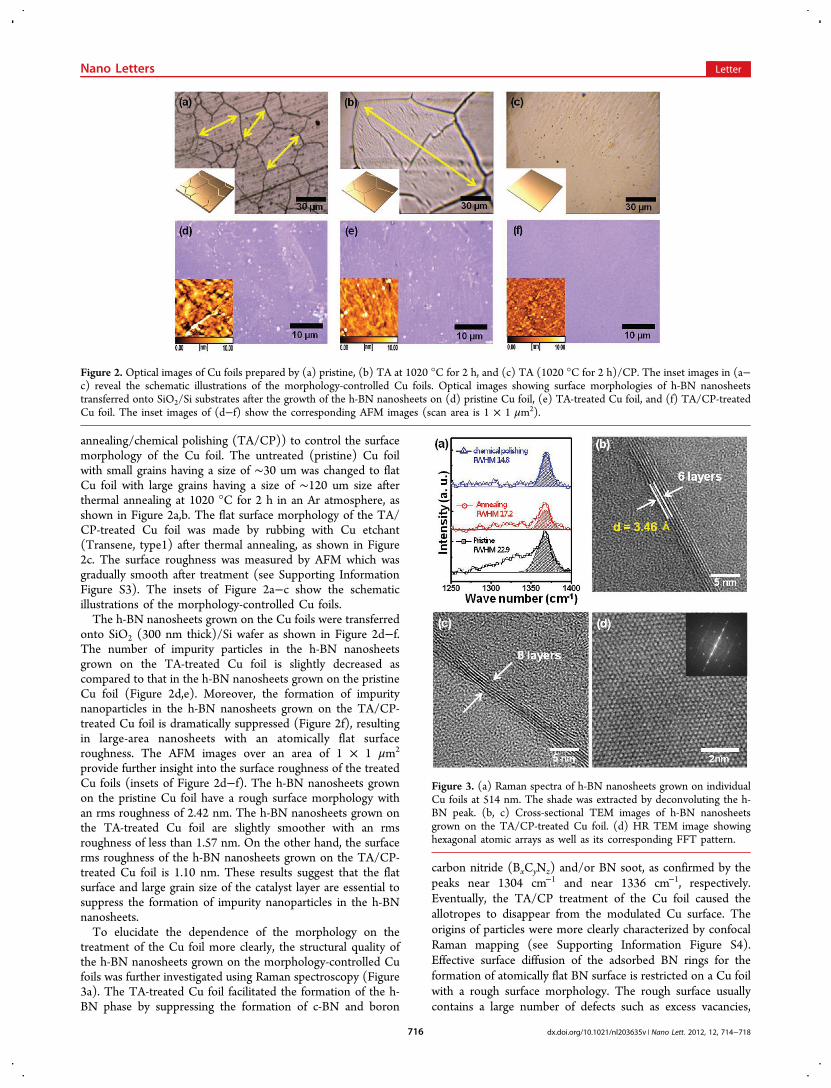
annealing/chemical polishing (TA/CP)) to control the surfacemorphology of the Cu foil. The untreated (pristine) Cu foilwith small grains having a size of ∼30 um was changed to flatCu foil with large grains having a size of ∼120 um size afterthermal annealing at 1020 °C for 2 h in an Ar atmosphere, asshown in Figure 2a,b. The flat surface morphology of the TA/CP-treated Cu foil was made by rubbing with Cu etchant(Transene, type1) after thermal annealing, as shown in Figure2c. The surface roughness was measured by AFM which wasgradually smooth after treatment (see Supporting InformationFigure S3). The insets of Figure 2a−c show the schematicillustrations of the morphology-controlled Cu foils.The h-BN nanosheets grown on the Cu foils were transferred
onto SiO2 (300 nm thick)/Si wafer as shown in Figure 2d−f.The number of impurity particles in the h-BN nanosheetsgrown on the TA-treated Cu foil is slightly decreased ascompared to that in the h-BN nanosheets grown on the pristineCu foil (Figure 2d,e). Moreover, the formation of impuritynanoparticles in the h-BN nanosheets grown on the TA/CP-treated Cu foil is dramatically suppressed (Figure 2f), resultingin large-area nanosheets with an atomically flat surfaceroughness. The AFM images over an area of 1 × 1 μm2
provide further insight into the surface roughness of the treatedCu foils (insets of Figure 2d−f). The h-BN nanosheets grownon the pristine Cu foil have a rough surface morphology withan rms roughness of 2.42 nm. The h-BN nanosheets grown onthe TA-treated Cu foil are slightly smoother with an rmsroughness of less than 1.57 nm. On the other hand, the surfacerms roughness of the h-BN nanosheets grown on the TA/CP-treated Cu foil is 1.10 nm. These results suggest that the flatsurface and large grain size of the catalyst layer are essential tosuppress the formation of impurity nanoparticles in the h-BNnanosheets.To elucidate the dependence of the morphology on the
treatment of the Cu foil more clearly, the structural quality ofthe h-BN nanosheets grown on the morphology-controlled Cufoils was further investigated using Raman spectroscopy (Figure3a). The TA-treated Cu foil facilitated the formation of the h-BN phase by suppressing the formation of c-BN and boron
carbon nitride (BxCyNz) and/or BN soot, as confirmed by thepeaks near 1304 cm−1 and near 1336 cm−1, respectively.Eventually, the TA/CP treatment of the Cu foil caused theallotropes to disappear from the modulated Cu surface. Theorigins of particles were more clearly characterized by confocalRaman mapping (see Supporting Information Figure S4).Effective surface diffusion of the adsorbed BN rings for theformation of atomically flat BN surface is restricted on a Cu foilwith a rough surface morphology. The rough surface usuallycontains a large number of defects such as excess vacancies,
Figure 2. Optical images of Cu foils prepared by (a) pristine, (b) TA at 1020 °C for 2 h, and (c) TA (1020 °C for 2 h)/CP. The inset images in (a−c) reveal the schematic illustrations of the morphology-controlled Cu foils. Optical images showing surface morphologies of h-BN nanosheetstransferred onto SiO2/Si substrates after the growth of the h-BN nanosheets on (d) pristine Cu foil, (e) TA-treated Cu foil, and (f) TA/CP-treatedCu foil. The inset images of (d−f) show the corresponding AFM images (scan area is 1 × 1 μm2).
Figure 3. (a) Raman spectra of h-BN nanosheets grown on individualCu foils at 514 nm. The shade was extracted by deconvoluting the h-BN peak. (b, c) Cross-sectional TEM images of h-BN nanosheetsgrown on the TA/CP-treated Cu foil. (d) HR TEM image showinghexagonal atomic arrays as well as its corresponding FFT pattern.
Nano Letters Letter
dx.doi.org/10.1021/nl203635v | Nano Lett. 2012, 12, 714−718716
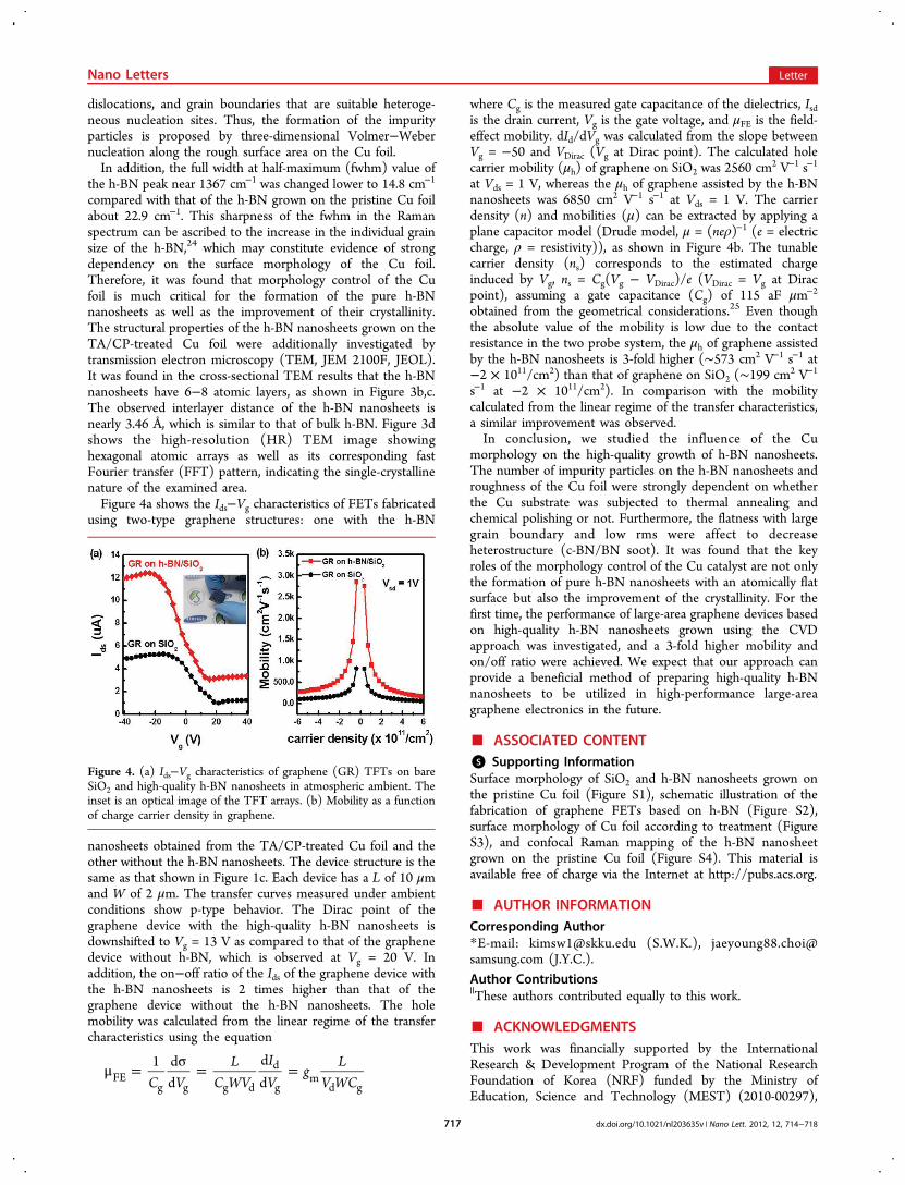
dislocations, and grain boundaries that are suitable heteroge-neous nucleation sites. Thus, the formation of the impurityparticles is proposed by three-dimensional Volmer−Webernucleation along the rough surface area on the Cu foil.In addition, the full width at half-maximum (fwhm) value of
the h-BN peak near 1367 cm−1 was changed lower to 14.8 cm−1
compared with that of the h-BN grown on the pristine Cu foilabout 22.9 cm−1. This sharpness of the fwhm in the Ramanspectrum can be ascribed to the increase in the individual grainsize of the h-BN,24 which may constitute evidence of strongdependency on the surface morphology of the Cu foil.Therefore, it was found that morphology control of the Cufoil is much critical for the formation of the pure h-BNnanosheets as well as the improvement of their crystallinity.The structural properties of the h-BN nanosheets grown on theTA/CP-treated Cu foil were additionally investigated bytransmission electron microscopy (TEM, JEM 2100F, JEOL).It was found in the cross-sectional TEM results that the h-BNnanosheets have 6−8 atomic layers, as shown in Figure 3b,c.The observed interlayer distance of the h-BN nanosheets isnearly 3.46 Å, which is similar to that of bulk h-BN. Figure 3dshows the high-resolution (HR) TEM image showinghexagonal atomic arrays as well as its corresponding fastFourier transfer (FFT) pattern, indicating the single-crystallinenature of the examined area.Figure 4a shows the Ids−Vg characteristics of FETs fabricated
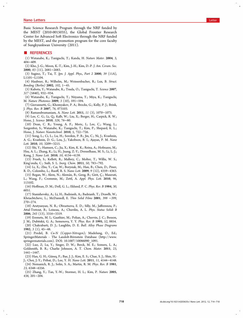
using two-type graphene structures: one with the h-BN
nanosheets obtained from the TA/CP-treated Cu foil and theother without the h-BN nanosheets. The device structure is thesame as that shown in Figure 1c. Each device has a L of 10 μmand W of 2 μm. The transfer curves measured under ambientconditions show p-type behavior. The Dirac point of thegraphene device with the high-quality h-BN nanosheets isdownshifted to Vg = 13 V as compared to that of the graphenedevice without h-BN, which is observed at Vg = 20 V. Inaddition, the on−off ratio of the Ids of the graphene device withthe h-BN nanosheets is 2 times higher than that of thegraphene device without the h-BN nanosheets. The holemobility was calculated from the linear regime of the transfercharacteristics using the equation
μ = σ = =C V
LC WV
IV
gL
V WC1 d
dddFE
g g g d
d
gm
d g
where Cg is the measured gate capacitance of the dielectrics, Isdis the drain current, Vg is the gate voltage, and μFE is the field-effect mobility. dId/dVg was calculated from the slope betweenVg = −50 and VDirac (Vg at Dirac point). The calculated holecarrier mobility (μh) of graphene on SiO2 was 2560 cm
2 V−1 s−1
at Vds = 1 V, whereas the μh of graphene assisted by the h-BNnanosheets was 6850 cm2 V−1 s−1 at Vds = 1 V. The carrierdensity (n) and mobilities (μ) can be extracted by applying aplane capacitor model (Drude model, μ = (neρ)−1 (e = electriccharge, ρ = resistivity)), as shown in Figure 4b. The tunablecarrier density (ns) corresponds to the estimated chargeinduced by Vg, ns = Cg(Vg − VDirac)/e (VDirac = Vg at Diracpoint), assuming a gate capacitance (Cg) of 115 aF μm−2
obtained from the geometrical considerations.25 Even thoughthe absolute value of the mobility is low due to the contactresistance in the two probe system, the μh of graphene assistedby the h-BN nanosheets is 3-fold higher (∼573 cm2 V−1 s−1 at−2 × 10¹¹/cm2) than that of graphene on SiO2 (∼199 cm2 V−1
s−1 at −2 × 10¹¹/cm2). In comparison with the mobilitycalculated from the linear regime of the transfer characteristics,a similar improvement was observed.In conclusion, we studied the influence of the Cu
morphology on the high-quality growth of h-BN nanosheets.The number of impurity particles on the h-BN nanosheets androughness of the Cu foil were strongly dependent on whetherthe Cu substrate was subjected to thermal annealing andchemical polishing or not. Furthermore, the flatness with largegrain boundary and low rms were affect to decreaseheterostructure (c-BN/BN soot). It was found that the keyroles of the morphology control of the Cu catalyst are not onlythe formation of pure h-BN nanosheets with an atomically flatsurface but also the improvement of the crystallinity. For thefirst time, the performance of large-area graphene devices basedon high-quality h-BN nanosheets grown using the CVDapproach was investigated, and a 3-fold higher mobility andon/off ratio were achieved. We expect that our approach canprovide a beneficial method of preparing high-quality h-BNnanosheets to be utilized in high-performance large-areagraphene electronics in the future.
■ ASSOCIATED CONTENT*S Supporting InformationSurface morphology of SiO2 and h-BN nanosheets grown onthe pristine Cu foil (Figure S1), schematic illustration of thefabrication of graphene FETs based on h-BN (Figure S2),surface morphology of Cu foil according to treatment (FigureS3), and confocal Raman mapping of the h-BN nanosheetgrown on the pristine Cu foil (Figure S4). This material isavailable free of charge via the Internet at http://pubs.acs.org.
■ AUTHOR INFORMATIONCorresponding Author*E-mail: [email protected] (S.W.K.), [email protected] (J.Y.C.).
Author Contributions||These authors contributed equally to this work.
■ ACKNOWLEDGMENTSThis work was financially supported by the InternationalResearch & Development Program of the National ResearchFoundation of Korea (NRF) funded by the Ministry ofEducation, Science and Technology (MEST) (2010-00297),
Figure 4. (a) Ids−Vg characteristics of graphene (GR) TFTs on bareSiO2 and high-quality h-BN nanosheets in atmospheric ambient. Theinset is an optical image of the TFT arrays. (b) Mobility as a functionof charge carrier density in graphene.
Nano Letters Letter
dx.doi.org/10.1021/nl203635v | Nano Lett. 2012, 12, 714−718717
Basic Science Research Program through the NRF funded bythe MEST (2010-0015035), the Global Frontier ResearchCenter for Advanced Soft Electronics through the NRF fundedby the MEST, and the promotion program for the core facultyof Sungkyunkwan University (2011).
■ REFERENCES(1) Watanabe, K.; Taniguchi, T.; Kanda, H. Nature Mater. 2004, 3,404−409.(2) Kho, J.-G.; Moon, K.-T.; Kim, J.-H.; Kim, D.-P. J. Am. Ceram. Soc.2000, 83 (11), 2681−2683.(3) Sugino, T.; Tai, T. Jpn. J. Appl. Phys., Part 2 2000, 39 (11A),L1101−L1104.(4) Haubner, R.; Wilhelm, M.; Weissenbacher, R.; Lux, B. Struct.Bonding (Berlin) 2002, 102, 1−45.(5) Kubota, Y.; Watanabe, K.; Tsuda, O.; Taniguchi, T. Science 2007,317 (5840), 932−934.(6) Watanabe, K.; Taniguchi, T.; Niiyama, T.; Miya, K.; Taniguchi,M. Nature Photonics 2009, 3 (10), 591−594.(7) Giovannetti, G.; Khomyakov, P. A.; Brocks, G.; Kelly, P. J.; Brink,J. Phys. Rev. B 2007, 76, 073103.(8) Ramasubramaniam, A. Nano Lett. 2011, 11 (3), 1070−1075.(9) Lee, C. G.; Li, Q.; Kalb, W.; Liu, X.; Berger, H.; Carpick, R. W.;Hone, J. Science 2010, 328, 76−80.(10) Dean, C. R.; Young, A. F.; Meric, I.; Lee, C.; Wang, L.;Sorgenfrei, S.; Watanabe, K.; Taniguchi, T.; Kim, P.; Shepard, K. L.;Hone, J. Nature Nanotechnol. 2010, 5, 722−726.(11) Song, L.; Ci, L.; Lu, H.; Sorokin, P. B.; Jin, C.; Ni, J.; Kvashnin,A. G.; Kvashnin, D. G.; Lou, J.; Yakobson, B. I.; Ajayan, P. M. NanoLett. 2010, 10, 3209−3215.(12) Shi, Y.; Hamsen, C.; Jia, X.; Kim, K. K.; Reina, A.; Hofmann, M.;Hsu, A. L.; Zhang, K.; Li, H.; Juang, Z.-Y.; Dresselhaus, M. S.; Li, L.-J.;Kong, J. Nano Lett. 2010, 10, 4134−4139.(13) Frueh, S.; Kellett, R.; Mallery, C.; Molter, T.; Willis, W. S.;King’ondu, C.; Suib, S. L. Inorg. Chem. 2011, 50, 783−792.(14) Li, X.; Zhu, Y.; Cai, W.; Borysiak, M.; Han, B.; Chen, D.; Piner,R. D.; Colombo, L.; Ruoff, R. S. Nano Lett. 2009, 9 (12), 4359−4363.(15) Regan, W.; Alem, N.; Aleman, B.; Geng, B.; Girit, C.; Maserati,L.; Wang, F.; Crommie, M.; Zettl, A. Appl. Phys. Lett. 2010, 96,113102.(16) Hoffman, D. M.; Doll, G. L.; Eklund, P. C. Phys. Rev. B 1984, 30,6051.(17) Stanishevsky, A.; Li, H.; Badzianb, A.; Badzianb, T.; Drawlb, W.;Khriachtchevc, L.; McDaniedl, E. Thin Solid Films 2001, 398 −399,270−274.(18) Arutyunyan, N. R.; Obraztsova, E. D.; Silly, M.; Jaffrennou, P.;Attal-Tretout, B.; Loiseau, A.; Chuvilin, A. L. Phys. Status Solidi B2006, 243 (13), 3316−3319.(19) Eremets, M. I.; Gauthier, M.; Polian, A.; Chervin, J. C.; Besson,J. M.; Dubitskii, G. A.; Semenova, Y. Y. Phys. Rev. B 1995, 52, 8854.(20) Chakrabarti, D. J.; Laughlin, D. E. Bull. Alloy Phase Diagrams1982, 3 (1), 45−48.(21) Predel, B. Cu-N (Copper-Nitrogen); Madelung, O., Ed.;SpringerMaterials - The Landolt-Bornstein Database (http://www.springermaterials.com). DOI: 10.1007/10086090_1091.(22) Luo, Z; Lu, Y.; Singer, D. W.; Berck, M. E.; Somers, L. A.;Goldsmith, B. R.; Charlie Johnson, A. T. Chem. Mater. 2011, 23,1441−1447.(23) Han, G. H.; Gunes, F.; Bae, J. J.; Kim, E. S.; Chae, S. J.; Shin, H.-J.; Choi, J.-Y.; Pribat, D.; Lee, Y. H. Nano Lett. 2011, 11, 4144−4148.(24) Nemanich, R. J.; Solin, S. A.; Martin, R. M. Phys. Rev. B 1981,23, 6348−6356.(25) Zhang, Y.; Tan, Y.-W.; Stormer, H. L.; Kim, P. Nature 2005,438, 201−204.
Nano Letters Letter
dx.doi.org/10.1021/nl203635v | Nano Lett. 2012, 12, 714−718718