Embed Size (px)
Citation preview
IEICE TRANS. FUNDAMENTALS, VOL.E103–A, NO.1 JANUARY 202011
PAPER Special Section on Cryptography and Information Security
Laser-Induced Controllable Instruction Replacement Fault Attack
Junichi SAKAMOTO†a), Student Member, Daisuke FUJIMOTO†b), and Tsutomu MATSUMOTO†c), Members
SUMMARY To develop countermeasures against fault attacks, it is im-portant to model an attacker’s ability. The instruction skip model is awell-studied practical model for fault attacks on software. Contrastingly,few studies have investigated the instruction replacement model, which is ageneralization of the instruction skip model, because replacing an instruc-tion with a desired one is considered difficult. Some previous studies havereported successful instruction replacements; however, those studies con-cluded that such instruction replacements are not practical attacks becausethe outcomes of the replacements are uncontrollable. This paper proposesthe concept of a controllable instruction replacement technique that usesthe laser irradiation of flash memory. The feasibility of the proposed tech-nique is demonstrated experimentally using a smartcard-type ARM SC100microcontroller. Then, practical cryptosystem attacks that exploit the pro-posed technique are investigated. The targeted cryptosystems employ theAES with software-based anti-fault countermeasures. We demonstrate thatan existing anti-instruction-skip countermeasure can be circumvented byreplacing a critical instruction, e.g., a branch instruction to detect fault oc-currence.key words: instruction replacement, instruction skip, fault attack, laserfault injection, side-channel attack
1. Introduction
The phrase “Trillion Sensor Universe,” which is increas-ingly used in the literature, suggests that the Internet ofThings era will involve an extremely large number of de-vices. In this situation, physical attacks on cryptosystemswill increase due to relatively easy physical access to de-vices. Physical attacks on cryptosystems can be classifiedas; side-channel attacks (passive attacks), and fault attacks(active attacks). This paper focuses on fault attacks, whichobtain stored secret data by intentionally injecting “faults”into the electronic circuit. For example, such faults can in-clude forcible output of secret data. To develop counter-measures against fault attacks, it is necessary to restrict at-tacker’s ability. This process is referred to as “attacker mod-eling,” and the modeled results are referred to as a “faultmodel.”
In this study, we focus on instruction skip and instruc-tion replacement models. The instruction skip model faults,which allows an attacker to skip an assembly language in-struction, has been observed on several embedded processorarchitectures and for several fault injection methods [1]–[5].
Manuscript received March 18, 2019.Manuscript revised July 4, 2019.†The authors are with Yokohama National University,
Yokohama-shi, 240-8501 Japan.a) E-mail: [email protected]) E-mail: [email protected]) E-mail: [email protected]
DOI: 10.1587/transfun.2019CIP0028
Actually, the instruction skip model, a widely studied com-mon fault model, is considered a subset of the instructionreplacement model, in which attackers can replace an as-sembly language instruction. Here, replacements to No Op-eration (NOP) instructions correspond to the instruction skip[6]. Previous studies have reported that instruction replace-ment faults as well as some instruction skip faults occur ondifferent architectures and through different fault injectionmeans [1], [3]. However, these faults should be referredto as instruction “corruption” rather than “replacement” be-cause replacing an instruction with one the attackers want isdifficult.
We propose the concept of a controllable instructionreplacement technique where a running instruction can bechange to a desired instruction. We demonstrate the feasibil-ity of the proposed concept experimentally on a smartcard-type ARM SC100 microcontroller. The primary contribu-tions of this study can be summarized as follows.
(I) Concept of controllable instruction replacement.To the best of our knowledge, the concept of how to injectcontrollable instruction replacement faults has not been de-scribed previously. In the proposed conceptualization, faultsare injected into instruction codes being fetched using laserirradiation on the flash memory from which the target in-struction codes are fetched. By using a laser to irradiate asense amplifier on flash memory, it is expected that a logicvalue (1/0) issued by the sense amplifier will become faulty.Here, we assume that the nth sense amplifier reads the nthbit of instruction code; thus, aiming the laser at sense am-plifiers enables us to control the position of the faulty bit ina replaced instruction.
(II) Demonstration of the feasibility of the proposedcontrollable instruction replacement concept. Laser ex-periments to demonstrate the concept of controllable in-struction replacement were performed on an ARM secureprocessor. A laser irradiation environment was set up tocontrol four laser parameters, i.e., irradiated point, duration,power and timing, to investigate how those parameters affectinstruction replacement.
(III) Circumventing existing countermeasuresagainst instruction skip using the controllable instruc-tion replacement. Most previous studies on fault at-tacks against software consider instruction skip as a generalfault model and propose attacks using and countermeasuresagainst instruction skip. Instruction replacement model isan upper level notion of instruction skip model. Thus, theproposed controllable instruction replacement could com-
Copyright c© 2020 The Institute of Electronics, Information and Communication Engineers
12IEICE TRANS. FUNDAMENTALS, VOL.E103–A, NO.1 JANUARY 2020
promise the security of existing countermeasures against in-struction skip attacks. We describe instruction replacementattacks that circumvent existing countermeasures against in-struction skip.
The remainder of this paper is organized as follows.Section 2 provides a brief overview of previous studies re-lated to fault attacks and fault model. Section 3 introducesthe concept of controllable instruction replacement based onlaser irradiation of a sense amplifier in flash memory (thecontribution (I)). The experimental setup used to demon-strate the feasibility of the proposed concept is describedin Sect. 4. In addition, experimental results using an ARMSC100 processor are provided (the contribution (II)). InSect. 5, we describe an attack on existing countermeasuresagainst instruction skip (the contribution (III)). Conclusionsand suggestions for future work are given in Sect. 6.
2. Related Works
To construct countermeasures against fault attacks, an at-tacker’s ability is abstracted as a “fault model.” As shown inTable 1, fault models are classified according to the levelat which the faults occur. As mentioned previously, thisstudy focuses on instruction skip and instruction replace-ment models.
2.1 Instruction Skip Model
Previous studies have reported the occurrence of instructionskip faults for several fault injection means on various de-vices, such as the clock glitch on the 8-bit AVR ATMega163[1] and LEON3 processor [2], electromagnetic irradiationon the 32-bit ARM Cortex-M3 [3] and the 32-bit ARMv7-Mdevice [4], and laser irradiation on the 32-bit ARM CortexM3 [5]. Moreover, instruction skip faults cause upper-levelIF skip and Loop Count skip faults. Differential fault anal-ysis (DFA) techniques, which computes the candidates of asecret key with sets of a correct (fault-free) ciphertext andan incorrect (fault-injected) ciphertext, are often proposedbased on these algorithmic level fault models; thus, the in-struction skip model is considered to be a practical and com-mon threat to software-implemented cryptosystems.
2.2 Instruction Replacement Model
In the instruction replacement model, attackers can replacea given instruction with a different instruction. The in-struction skip model can be considered part of the instruc-tion replacement model wherein a target instruction is re-placed with a NOP instruction. Compared to the instruc-tion skip model, the instruction replacement model repre-sents significant threat. As mentioned previously, someexperimental results reported that instruction replacementfaults were observed on some devices. However, few studiesfocus primarily on instruction replacement and none con-sider developing countermeasures against the instruction re-placements. Balasch et al. reported the occurrence of in-
Table 1 Fault models. The lower (the bottom in the figure) level faultscauses the upper level faults.
Fault level Fault model Main target
Algorithmic IF skip SoftwareLoop Count skip
Instruction Instruction skipInstruction replacement
Register Bits stuck-at/flip/random HardwareTransistor Set/reset/flip
Table 2 Comparison of the proposed method and previous instructionreplacement studies.
Fault injectionmean
Instruction replace-ment timing
Instructions af-ter replacement
[1] Clock glitch Controllable Not controllable[3] EM irradiation Controllable Not controllable[7] Underpowering Not controllable ControllableOurs Laser irradiation Controllable Controllable
struction replacements on an ATMega163 smartcard via aclock glitch at the time of instruction pre-fetch [1]. Intheir study, some instructions, e.g., EOR (Exclusive OR)and SER (SEt all bits in Register), were targeted, and theinstructions after replacement depend on the period of theclock glitch. However, Balasch et al. concluded that con-trolling instructions after replacement is highly complex be-cause it depends on the internal state of the MCU. Similarresults were observed by Moro et al. on an ARM Cortex-M3 microcontroller through electromagnetic glitches [3].Similar to Balasch et al., Moro et al. could not controlinstructions after replacement. On an ARM9 microcon-troller, Barenghi et al. achieved more practical instructionreplacements through underpowering the target device [7].In their experiments, 1-bit stuck-at-0 faults were observedduring instruction fetch, and they claimed that their methodcould produce instruction replacements, such as replacingan AND instruction with an EOR instruction. However, astheir proposed method reduces the supply voltage during en-tire program execution, it is not possible to select instruc-tions to be fault-injected (i.e. instruction replacement tim-ing).
Table 2 compares the proposed method to previousstudies about instruction replacement. As can be seen, in-struction replacements in the previous studies can only con-trol either instructions replacement timing or instructions af-ter replacement. We propose a controllable instruction re-placement method that can control both instruction replace-ment timing and instructions after replacement.
3. Proposed Method: Controllable Instruction Re-placement by Irradiating Sense Amplifier in FlashMemory with Laser
This section explains the basic concept behind producingthe controllable instruction replacement, i.e., the laser irra-diation of a sense amplifier on a flash memory chip. Mostelectronic devices with cryptographic modules include flash
SAKAMOTO et al.: LASER-INDUCED CONTROLLABLE INSTRUCTION REPLACEMENT FAULT ATTACK13
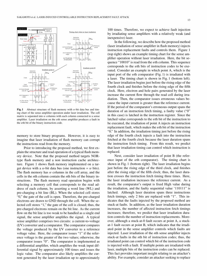
Fig. 1 Abstract structure of flash memory with w-bit data bus and tim-ing chart of the sense amplifier operation under laser irradiation. The cellmatrix is separated into w columns with each column connected to a senseamplifier. Laser irradiation on the wth sense amplifier produces a fault inthe wth bit of the binary instruction code.
memory to store binary programs. However, it is easy toimagine that laser irradiation of flash memory can corruptthe instructions read from the memory.
Prior to introducing the proposed method, we first ex-plain the structure and read operation of a typical flash mem-ory device. Note that the proposed method targets NOR-type flash memory and a non instruction cache architec-ture. Figure 1 shows flash memory implemented on a tar-get device with a w-bit data bus (one instruction = w bits).The flash memory has w columns in the cell array, and thecells in the nth column contain the nth bits of the binary in-structions. The flash memory read operation begins withselecting a memory cell that corresponds to the read ad-dress of each column, by asserting a word line (WL) andpre-charging a bit line (BL). When the selected cell stores“0,” the gate of the cell is open. Therefore, the pre-chargedelectrons are drawn to GND through the cell. When the se-lected cell stores “1,” the gate of the cell is closed; thus, thepre-charged electrons remain on the bit line. As the currentflow on the bit line is too weak to be handled as a single endsignal, the sense amplifier amplifies the signal. A typicalsense amplifier comprises two circuits: a current-to-voltage(I/V) converter and a comparator. The comparator comparesthe voltage produced by the I/V converter to a referencevoltage value. Here, the comparator issues “1” if the refer-ence voltage is the greater of the two values; otherwise, thecomparator issues “0”. The comparator is implemented asa differential amplifier, which amplifies the weak input dif-ferential signal by approximately 100 times and issues thelogic value. The comparator also likely amplifies the cur-rent generated by the laser irradiation up to approximately
100 times. Therefore, we expect to achieve fault injectionby irradiating sense amplifiers with a relatively weak (andinexpensive) laser.
In the following, we describe how the proposed method(laser irradiation of sense amplifier in flash memory) injectsinstruction replacement faults and controls them. Figure 1(top right) shows an example timing chart for the sense am-plifier operation without laser irradiation. Here, the bit se-quence “10010” is read from the wth column. This sequencecorresponds to the wth bits of instruction codes to be exe-cuted. Consider an example in which point A, which is theinput port of the wth comparator (Fig. 1) is irradiated witha laser. The timing chart is shown in Fig. 1 (bottom left).The laser irradiation begins just before the rising edge of thefourth clock and finishes before the rising edge of the fifthclock. Here, electron and hole pairs generated by the laserincrease the current flow through the read cell during irra-diation. Then, the comparator issues erroneous values be-cause the input current is greater than the reference current.If the period of the comparator’s erroneous output spans theduration of an instruction fetch timing, a faulty value (“0”in this case) is latched in the instruction register. Since thelatched value corresponds to the wth bit of the instruction tobe executed, the irradiation of point A injects an instructionreplacement fault, which makes the wth bit of the instruction“0.” In addition, the irradiation timing just before the risingedge of the fourth clock injects a fault into the instructionfetched at the fourth clock because the laser duration spansthe instruction fetch timing. From this result, we predictthat laser irradiation timing can control which instruction isreplaced.
Next, consider laser irradiation of point B (the refer-ence input of the wth comparator). The timing chart isshown in Fig. 1 (bottom right). The laser irradiation beginsjust before the rising edge of the third clock, and finishesafter the rising edge of the fifth clock; thus, the laser dura-tion crosses the instruction fetch timing three times. Here,the laser irradiation increases the reference current. As aresult, the comparator’s output is fixed High value duringthe irradiation, and the faulty sequential value ‘110111” islatched. Although laser duration spans three instructionsfetch timings, only 2 bits are replaced with “1”. This in-dicates that the faults injected by the proposed method arestuck-at faults. In addition, as the laser irradiation durationincreases, the number of affected instruction fetch timingsincreases; therefore, we predict that laser irradiation dura-tion controls the number of instruction replacements. More-over, although a stuck-at-0 fault occurs at point A, a stuck-at-1 fault occurs at point B, which indicates that the irradi-ated point in the sense amplifier controls which faults areinjected. Laser irradiation of the nth sense amplifier injectsstuck-at faults in the nth bit of instruction codes; thus, theirradiated point can control which bit of the instruction codeis injected with a fault. If multiple points are irradiated withlaser, multiple bits of the instruction codes can be replaced.This fact provides important insight relating to an attacker’sability. For example, consider an attacker seeking to replace
14IEICE TRANS. FUNDAMENTALS, VOL.E103–A, NO.1 JANUARY 2020
instruction Inss with instruction Insd. The number N of ir-radiated point required to replace Inss with Insd is the Ham-ming distance between the binary representation of Inss andInsd. A greater N value enhances the attacker’s ability butincreases the cost of the attack. For commercially availablelaser attack evaluation setup, N = 1 or N = 2. If N isgreater than two, the optics becomes too complicated to de-sign and construct a feasible experiment. In the experimentsdiscussed in Sect. 4, we demonstrate the proposed methodin the case of N = 1.
In the proposed controllable instruction replacementmethod, the following laser parameters control instructionreplacement: (i) the laser irradiation point controls whichbits are replaced with which value (“0” or “1”); (ii) the laserirradiation duration controls the number of instructions tobe replaced; (iii) the laser irradiation timing controls whichinstructions are replaced. Section 4 discusses experimentsconducted to confirm these points for N = 1 case.
4. Demonstration on an ARM Secure Processor
4.1 Experimental Environment
Here, we describe the laser setup and device under test(DUT) used in our instruction replacement experiments.The laser setup was optimized for backside laser irradia-tion. Note that devices manufactured using recent tech-nology have multiple metal layers that function as shieldsagainst laser beams. To avoid the effects of these metal lay-ers, the laser in the experimental setup was fired from thebackside of the DUT, i.e., from the silicon substrate side.In this experiment, a smartcard-type ARM SC100 device isused as the DUT because it is easy to expose the siliconsubstrate of smartcard; thus, such devices are suitable forbackside laser irradiation.
4.1.1 Laser Setup
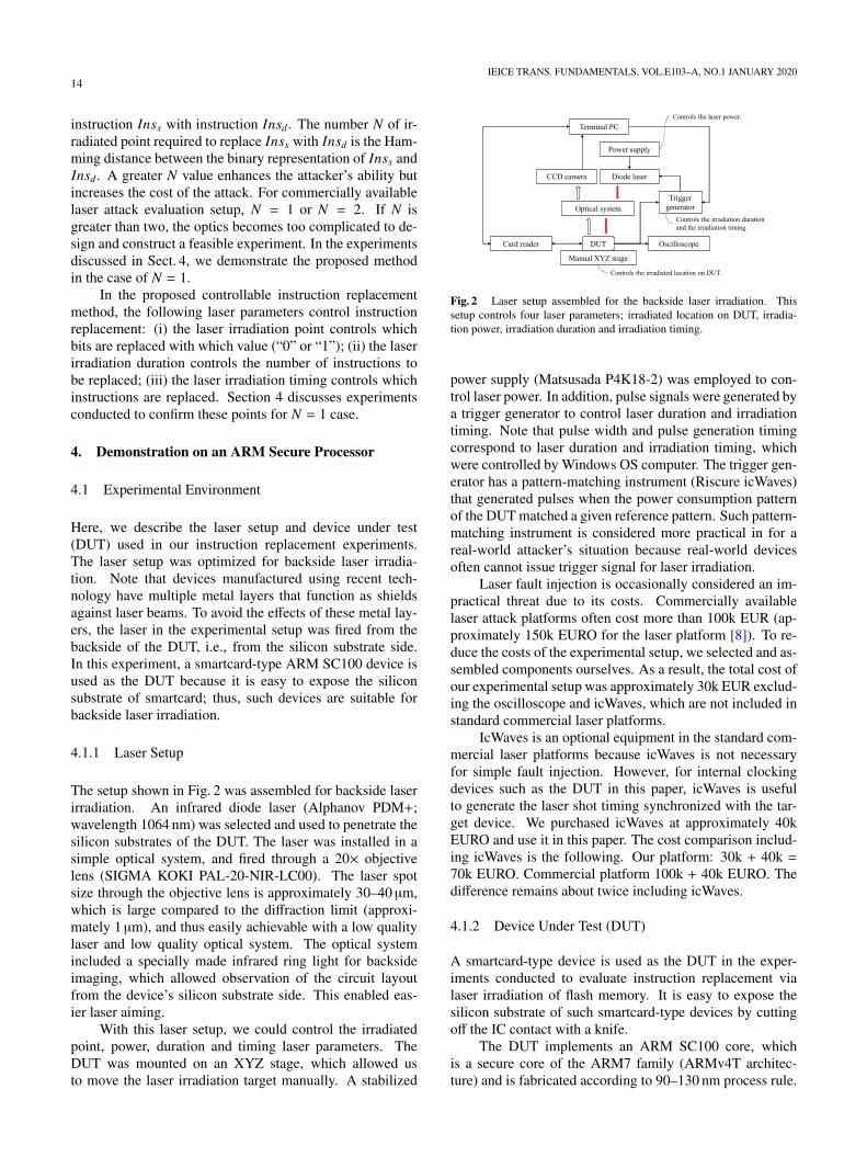
The setup shown in Fig. 2 was assembled for backside laserirradiation. An infrared diode laser (Alphanov PDM+;wavelength 1064 nm) was selected and used to penetrate thesilicon substrates of the DUT. The laser was installed in asimple optical system, and fired through a 20× objectivelens (SIGMA KOKI PAL-20-NIR-LC00). The laser spotsize through the objective lens is approximately 30–40 µm,which is large compared to the diffraction limit (approxi-mately 1 µm), and thus easily achievable with a low qualitylaser and low quality optical system. The optical systemincluded a specially made infrared ring light for backsideimaging, which allowed observation of the circuit layoutfrom the device’s silicon substrate side. This enabled eas-ier laser aiming.
With this laser setup, we could control the irradiatedpoint, power, duration and timing laser parameters. TheDUT was mounted on an XYZ stage, which allowed usto move the laser irradiation target manually. A stabilized
Fig. 2 Laser setup assembled for the backside laser irradiation. Thissetup controls four laser parameters; irradiated location on DUT, irradia-tion power, irradiation duration and irradiation timing.
power supply (Matsusada P4K18-2) was employed to con-trol laser power. In addition, pulse signals were generated bya trigger generator to control laser duration and irradiationtiming. Note that pulse width and pulse generation timingcorrespond to laser duration and irradiation timing, whichwere controlled by Windows OS computer. The trigger gen-erator has a pattern-matching instrument (Riscure icWaves)that generated pulses when the power consumption patternof the DUT matched a given reference pattern. Such pattern-matching instrument is considered more practical in for areal-world attacker’s situation because real-world devicesoften cannot issue trigger signal for laser irradiation.
Laser fault injection is occasionally considered an im-practical threat due to its costs. Commercially availablelaser attack platforms often cost more than 100k EUR (ap-proximately 150k EURO for the laser platform [8]). To re-duce the costs of the experimental setup, we selected and as-sembled components ourselves. As a result, the total cost ofour experimental setup was approximately 30k EUR exclud-ing the oscilloscope and icWaves, which are not included instandard commercial laser platforms.
IcWaves is an optional equipment in the standard com-mercial laser platforms because icWaves is not necessaryfor simple fault injection. However, for internal clockingdevices such as the DUT in this paper, icWaves is usefulto generate the laser shot timing synchronized with the tar-get device. We purchased icWaves at approximately 40kEURO and use it in this paper. The cost comparison includ-ing icWaves is the following. Our platform: 30k + 40k =
70k EURO. Commercial platform 100k + 40k EURO. Thedifference remains about twice including icWaves.
4.1.2 Device Under Test (DUT)
A smartcard-type device is used as the DUT in the exper-iments conducted to evaluate instruction replacement vialaser irradiation of flash memory. It is easy to expose thesilicon substrate of such smartcard-type devices by cuttingoff the IC contact with a knife.
The DUT implements an ARM SC100 core, whichis a secure core of the ARM7 family (ARMv4T architec-ture) and is fabricated according to 90–130 nm process rule.
SAKAMOTO et al.: LASER-INDUCED CONTROLLABLE INSTRUCTION REPLACEMENT FAULT ATTACK15
ARM7 family is a relatively old; however, it has been imple-mented on a number of devices, such as cellular phones andSIM cards. The ARM7 family applies the von Neumannarchitecture and a three-stage pipeline, i.e., fetch, decode,and execution. On the DUT, data and programs are storedin the same memory space, and memory instructions andbranch instructions take a few cycles, whereas ALU instruc-tions complete within a single cycle. Note that no memoryprotection or cache mechanisms were employed in these ex-periments. Here, the fetch stage was targeted for laser irradi-ation to replace the instructions to be executed. The SC100core is a secure core; thus, it is conjectured that some anti-tamper mechanism is implemented in this device. However,the flash memory is considered a peripheral unit; therefore,we predict that the proposed instruction replacement methodis feasible on the DUT.
The DUT has 64 KB ROM and 4 KB RAM for userspace, in which the experimental test programs were stored.An internal clock operates the DUT, and its frequency wasestimated as approximately 9 MHz by oscilloscope mea-surement. Relative to other security mechanisms, the DUTemploys data storage scrambling, abnormal voltage detec-tors (VD) and abnormal clock frequency detectors (FD). Theexperiments discussed in the following section were all con-ducted with the VD and FD enabled.
4.2 Experiments
In this section, we demonstrate controllable instruction re-placement through laser irradiation of flash memory on theDUT. Here, three laser parameters, irradiated point on theDUT, duration, and timing, were examined to confirm howthey affect the instruction replacement.
4.2.1 Effects of Irradiated Points
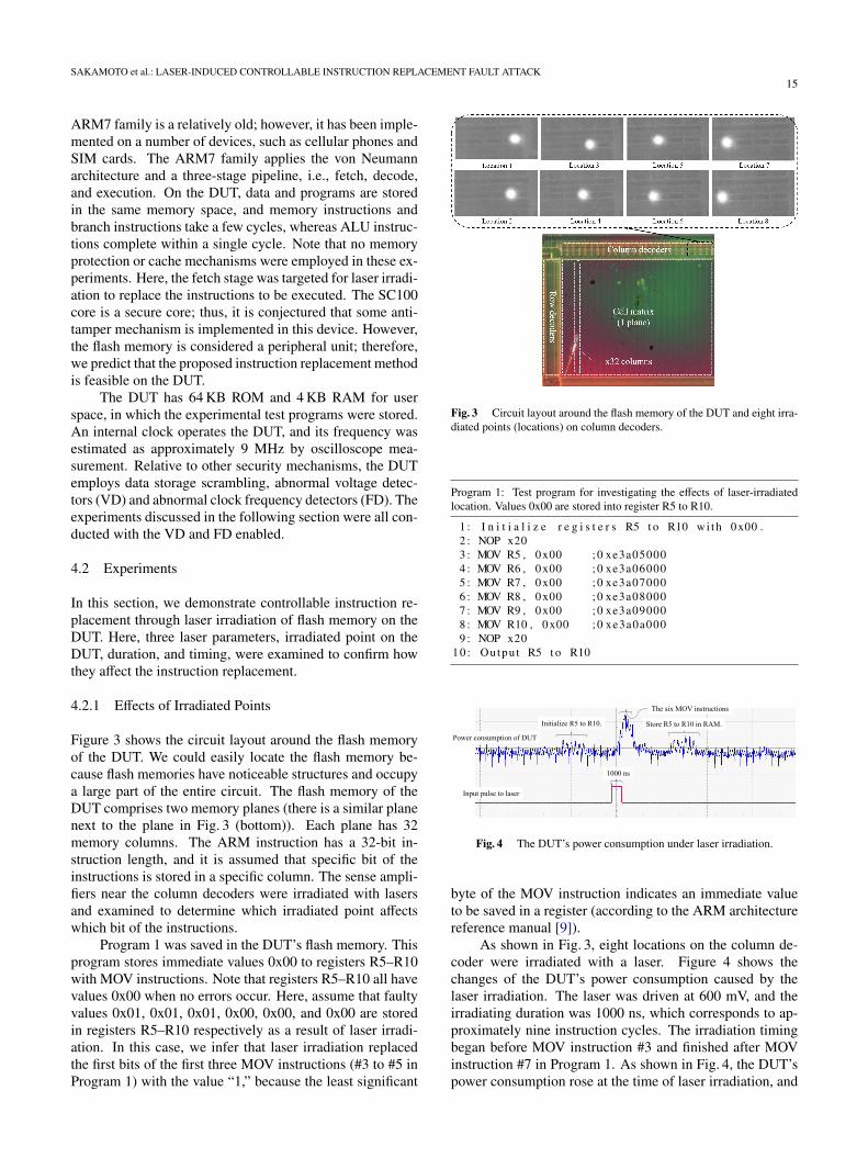
Figure 3 shows the circuit layout around the flash memoryof the DUT. We could easily locate the flash memory be-cause flash memories have noticeable structures and occupya large part of the entire circuit. The flash memory of theDUT comprises two memory planes (there is a similar planenext to the plane in Fig. 3 (bottom)). Each plane has 32memory columns. The ARM instruction has a 32-bit in-struction length, and it is assumed that specific bit of theinstructions is stored in a specific column. The sense ampli-fiers near the column decoders were irradiated with lasersand examined to determine which irradiated point affectswhich bit of the instructions.
Program 1 was saved in the DUT’s flash memory. Thisprogram stores immediate values 0x00 to registers R5–R10with MOV instructions. Note that registers R5–R10 all havevalues 0x00 when no errors occur. Here, assume that faultyvalues 0x01, 0x01, 0x01, 0x00, 0x00, and 0x00 are storedin registers R5–R10 respectively as a result of laser irradi-ation. In this case, we infer that laser irradiation replacedthe first bits of the first three MOV instructions (#3 to #5 inProgram 1) with the value “1,” because the least significant
Fig. 3 Circuit layout around the flash memory of the DUT and eight irra-diated points (locations) on column decoders.
Program 1: Test program for investigating the effects of laser-irradiatedlocation. Values 0x00 are stored into register R5 to R10.
1 : I n i t i a l i z e r e g i s t e r s R5 t o R10 wi th 0x00 .2 : NOP x203 : MOV R5 , 0x00 ; 0 xe3a050004 : MOV R6 , 0x00 ; 0 xe3a060005 : MOV R7 , 0x00 ; 0 xe3a070006 : MOV R8 , 0x00 ; 0 xe3a080007 : MOV R9 , 0x00 ; 0 xe3a090008 : MOV R10 , 0x00 ; 0 xe3a0a0009 : NOP x20
1 0 : Outpu t R5 t o R10
Fig. 4 The DUT’s power consumption under laser irradiation.
byte of the MOV instruction indicates an immediate valueto be saved in a register (according to the ARM architecturereference manual [9]).
As shown in Fig. 3, eight locations on the column de-coder were irradiated with a laser. Figure 4 shows thechanges of the DUT’s power consumption caused by thelaser irradiation. The laser was driven at 600 mV, and theirradiating duration was 1000 ns, which corresponds to ap-proximately nine instruction cycles. The irradiation timingbegan before MOV instruction #3 and finished after MOVinstruction #7 in Program 1. As shown in Fig. 4, the DUT’spower consumption rose at the time of laser irradiation, and
16IEICE TRANS. FUNDAMENTALS, VOL.E103–A, NO.1 JANUARY 2020
Table 3 Faulty values by laser irradiation (dependent on the eight irradi-ated locations).
Location R5 R6 R7 R8 R9 R10
1 0x10 0x00 0x10 0x00 0x10 0x002 0x20 0x00 0x20 0x00 0x20 0x003 0x80 0x00 0x80 0x00 0x80 0x004 0x40 0x00 0x40 0x00 0x40 0x005 0x01 0x00 0x01 0x00 0x01 0x006 0x02 0x00 0x02 0x00 0x02 0x007 0x08 0x00 0x08 0x00 0x08 0x008 0x04 0x00 0x04 0x00 0x04 0x00
the laser irradiation affected the timing of executing MOVinstructions. Table 3 shows the execution results of Pro-gram 1 for each irradiated location. Compared to the nor-mal execution result of 0x00 0x00 0x00 0x00 0x00 0x00,the values in registers R5, R7, and R9 showed a differenceof one bit from the original immediate value 0x00. Theseresults indicate that laser irradiation replaced one bit of theimmediate value field of the MOV instructions with value“1”; thus, faulty MOV instructions were executed. The posi-tions of the faulty bits of the machine code are dependent onthe irradiated location, e.g., irradiated location 1 makes thefifth bit of the 32-bit machine code faulty. While faults wereinjected in R5, R7 and R9, no faults occurred in R6, R8 orR10. Continuing the experiment, it was found that the eightirradiated locations only affected instructions stored in evenmemory addresses. By further experiment, we identified theirradiated locations that only affect instructions stored in oddmemory addresses.
Next, the same experiment was conducted with a dif-ferent program, in which the immediate value 0x00 of Pro-gram 1 was rewritten as 0xFF. The results demonstrate thatno faults occurred on irradiated locations 1–8, which indi-cates that the replacements by laser irradiation at these loca-tions were stuck-at-1 faults rather than bit-flip faults. Sincethe targeted immediate values were 0xFF (all bits 1), stuck-at-1 faults on the immediate field of MOV instruction hadno effect on the instructions. On the other hand, stuck-at-0faults were observed at the upper area of each location 1–8.By performing the same experiments on other irradiated lo-cations, we could specify which irradiated locations causestuck-at-0/1 faults into each bit of 32-bit machine code.Moreover by performing the same experiments to severalinstructions (ALU, memory operation, and branch instruc-tions), it was observed that the instruction replacements oc-cur except MOV instruction, too. Figure 5 summarizes theresults, where irradiated points are represented as a set of co-ordinates (X, Y). Laser irradiation of the points on the right16 column decoders of the 32 memory columns made theinstructions stored in even memory addresses faulty. Laserirradiation of the locations on the left 16 column decodersof the 32 memory columns made the instruction stored inodd memory addresses faulty. This is conjectured due to thebus-scramble mechanism implemented on the DUT or thetwo-plane memory structure. The left and right 16 columnsof the 32 columns both have 64 points that are sensitive to
Fig. 5 Relationships among laser-irradiated points and faulty bit posi-tions of the 32-bit instruction. The laser irradiation of coordinates (X, Y)injects stuck-at-Y fault to the Xth bit of the 32-bit instruction. The order ofthe fault-injected bit for the irradiated points shows the same pattern every1 byte. This figure shows irradiated points affecting the least significantbyte.
laser (stuck-at-0 points of each 32 bit and stuck-at-1 pointsof each 32 bit). The following describes the irradiated pointsin the right 16 columns because the irradiated points in bothright/left 16 columns have the same pattern.
For the irradiated points represented as the set of XYcoordinates, the Y coordinate of the irradiated points de-termines that the injected faults are stuck-at-0 or stuck-at-1faults. There were two Y coordinates sensitive to laser irra-diation, i.e., Y = 0 and Y = 1. Laser irradiation of points atY = 0 injects stuck-at-0 faults to a bit of the 32-bit machinecodes. In contrast, laser irradiation of points at Y = 1 injectsstuck-at-1 faults to a bit of the 32-bit machine code. TheX coordinate of the irradiated points determines the fault-injected bit position of the 32-bit machine code. The 64 ir-radiated points in the 16 columns demonstrate a pattern, i.e.,16 points are found in each of the four columns, as shownin Fig. 5. Figure 5 (top) shows the 16 points in the firstfour columns. Laser irradiation of these 16 points causeda stuck-at-0/1 fault in the least significant byte of the 32-bitmachine code. Note that laser irradiation of coordinate X= N corresponds to the Nth bit fault of the 32-bit machinecode. The same irradiated point pattern can be observed inother four columns. The 16 irradiated points in the secondfour columns replaced each bit of the second byte of the 32-bit machine code with “0/1,” which was also observed forthe third and fourth bytes. In this mean, we could specifythe 64 irradiated points that injected stuck-at-0/1 faults toeach bit of the 32-bit machine code stored in even memoryaddresses (as well as the 64 irradiated points affecting the32-bit machine code stored in odd memory addresses).
Relative to the memory address and bit order, the ex-perimental results differ slightly from the expected resultsexplained in Sect. 3. We consider that this was due to theinfluence of bus scramble security mechanism implemented
SAKAMOTO et al.: LASER-INDUCED CONTROLLABLE INSTRUCTION REPLACEMENT FAULT ATTACK17
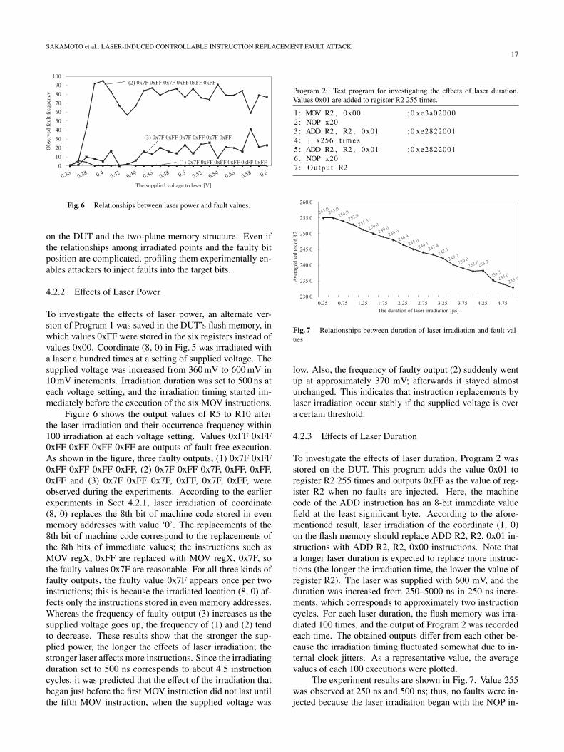
Fig. 6 Relationships between laser power and fault values.
on the DUT and the two-plane memory structure. Even ifthe relationships among irradiated points and the faulty bitposition are complicated, profiling them experimentally en-ables attackers to inject faults into the target bits.
4.2.2 Effects of Laser Power
To investigate the effects of laser power, an alternate ver-sion of Program 1 was saved in the DUT’s flash memory, inwhich values 0xFF were stored in the six registers instead ofvalues 0x00. Coordinate (8, 0) in Fig. 5 was irradiated witha laser a hundred times at a setting of supplied voltage. Thesupplied voltage was increased from 360 mV to 600 mV in10 mV increments. Irradiation duration was set to 500 ns ateach voltage setting, and the irradiation timing started im-mediately before the execution of the six MOV instructions.
Figure 6 shows the output values of R5 to R10 afterthe laser irradiation and their occurrence frequency within100 irradiation at each voltage setting. Values 0xFF 0xFF0xFF 0xFF 0xFF 0xFF are outputs of fault-free execution.As shown in the figure, three faulty outputs, (1) 0x7F 0xFF0xFF 0xFF 0xFF 0xFF, (2) 0x7F 0xFF 0x7F, 0xFF, 0xFF,0xFF and (3) 0x7F 0xFF 0x7F, 0xFF, 0x7F, 0xFF, wereobserved during the experiments. According to the earlierexperiments in Sect. 4.2.1, laser irradiation of coordinate(8, 0) replaces the 8th bit of machine code stored in evenmemory addresses with value ‘0’. The replacements of the8th bit of machine code correspond to the replacements ofthe 8th bits of immediate values; the instructions such asMOV regX, 0xFF are replaced with MOV regX, 0x7F, sothe faulty values 0x7F are reasonable. For all three kinds offaulty outputs, the faulty value 0x7F appears once per twoinstructions; this is because the irradiated location (8, 0) af-fects only the instructions stored in even memory addresses.Whereas the frequency of faulty output (3) increases as thesupplied voltage goes up, the frequency of (1) and (2) tendto decrease. These results show that the stronger the sup-plied power, the longer the effects of laser irradiation; thestronger laser affects more instructions. Since the irradiatingduration set to 500 ns corresponds to about 4.5 instructioncycles, it was predicted that the effect of the irradiation thatbegan just before the first MOV instruction did not last untilthe fifth MOV instruction, when the supplied voltage was
Program 2: Test program for investigating the effects of laser duration.Values 0x01 are added to register R2 255 times.
1 : MOV R2 , 0x00 ; 0 xe3a020002 : NOP x203 : ADD R2 , R2 , 0x01 ; 0 xe28220014 : | x256 t i m e s5 : ADD R2 , R2 , 0x01 ; 0 xe28220016 : NOP x207 : Outpu t R2
Fig. 7 Relationships between duration of laser irradiation and fault val-ues.
low. Also, the frequency of faulty output (2) suddenly wentup at approximately 370 mV; afterwards it stayed almostunchanged. This indicates that instruction replacements bylaser irradiation occur stably if the supplied voltage is overa certain threshold.
4.2.3 Effects of Laser Duration
To investigate the effects of laser duration, Program 2 wasstored on the DUT. This program adds the value 0x01 toregister R2 255 times and outputs 0xFF as the value of reg-ister R2 when no faults are injected. Here, the machinecode of the ADD instruction has an 8-bit immediate valuefield at the least significant byte. According to the afore-mentioned result, laser irradiation of the coordinate (1, 0)on the flash memory should replace ADD R2, R2, 0x01 in-structions with ADD R2, R2, 0x00 instructions. Note thata longer laser duration is expected to replace more instruc-tions (the longer the irradiation time, the lower the value ofregister R2). The laser was supplied with 600 mV, and theduration was increased from 250–5000 ns in 250 ns incre-ments, which corresponds to approximately two instructioncycles. For each laser duration, the flash memory was irra-diated 100 times, and the output of Program 2 was recordedeach time. The obtained outputs differ from each other be-cause the irradiation timing fluctuated somewhat due to in-ternal clock jitters. As a representative value, the averagevalues of each 100 executions were plotted.
The experiment results are shown in Fig. 7. Value 255was observed at 250 ns and 500 ns; thus, no faults were in-jected because the laser irradiation began with the NOP in-
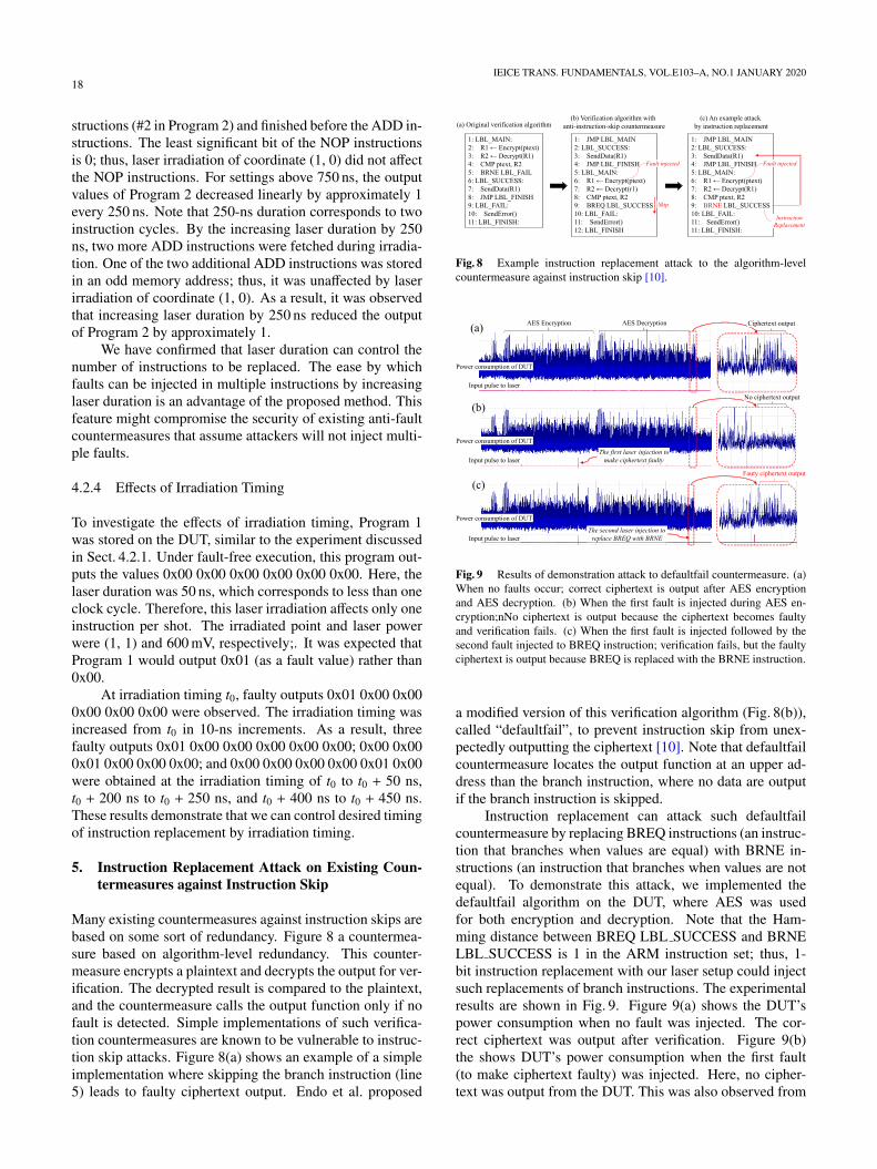
18IEICE TRANS. FUNDAMENTALS, VOL.E103–A, NO.1 JANUARY 2020
structions (#2 in Program 2) and finished before the ADD in-structions. The least significant bit of the NOP instructionsis 0; thus, laser irradiation of coordinate (1, 0) did not affectthe NOP instructions. For settings above 750 ns, the outputvalues of Program 2 decreased linearly by approximately 1every 250 ns. Note that 250-ns duration corresponds to twoinstruction cycles. By the increasing laser duration by 250ns, two more ADD instructions were fetched during irradia-tion. One of the two additional ADD instructions was storedin an odd memory address; thus, it was unaffected by laserirradiation of coordinate (1, 0). As a result, it was observedthat increasing laser duration by 250 ns reduced the outputof Program 2 by approximately 1.
We have confirmed that laser duration can control thenumber of instructions to be replaced. The ease by whichfaults can be injected in multiple instructions by increasinglaser duration is an advantage of the proposed method. Thisfeature might compromise the security of existing anti-faultcountermeasures that assume attackers will not inject multi-ple faults.
4.2.4 Effects of Irradiation Timing
To investigate the effects of irradiation timing, Program 1was stored on the DUT, similar to the experiment discussedin Sect. 4.2.1. Under fault-free execution, this program out-puts the values 0x00 0x00 0x00 0x00 0x00 0x00. Here, thelaser duration was 50 ns, which corresponds to less than oneclock cycle. Therefore, this laser irradiation affects only oneinstruction per shot. The irradiated point and laser powerwere (1, 1) and 600 mV, respectively;. It was expected thatProgram 1 would output 0x01 (as a fault value) rather than0x00.
At irradiation timing t0, faulty outputs 0x01 0x00 0x000x00 0x00 0x00 were observed. The irradiation timing wasincreased from t0 in 10-ns increments. As a result, threefaulty outputs 0x01 0x00 0x00 0x00 0x00 0x00; 0x00 0x000x01 0x00 0x00 0x00; and 0x00 0x00 0x00 0x00 0x01 0x00were obtained at the irradiation timing of t0 to t0 + 50 ns,t0 + 200 ns to t0 + 250 ns, and t0 + 400 ns to t0 + 450 ns.These results demonstrate that we can control desired timingof instruction replacement by irradiation timing.
5. Instruction Replacement Attack on Existing Coun-termeasures against Instruction Skip
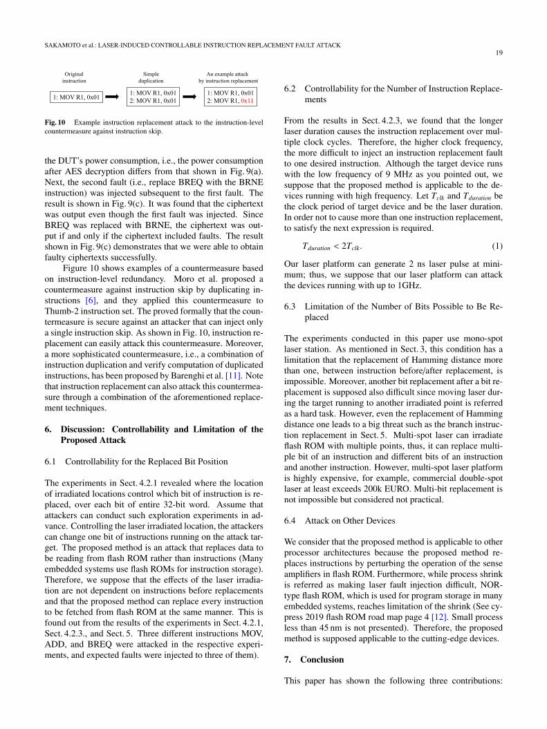
Many existing countermeasures against instruction skips arebased on some sort of redundancy. Figure 8 a countermea-sure based on algorithm-level redundancy. This counter-measure encrypts a plaintext and decrypts the output for ver-ification. The decrypted result is compared to the plaintext,and the countermeasure calls the output function only if nofault is detected. Simple implementations of such verifica-tion countermeasures are known to be vulnerable to instruc-tion skip attacks. Figure 8(a) shows an example of a simpleimplementation where skipping the branch instruction (line5) leads to faulty ciphertext output. Endo et al. proposed
Fig. 8 Example instruction replacement attack to the algorithm-levelcountermeasure against instruction skip [10].
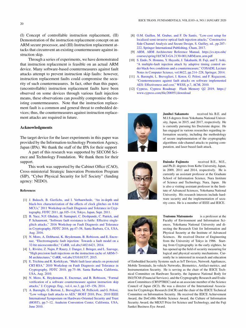
Fig. 9 Results of demonstration attack to defaultfail countermeasure. (a)When no faults occur; correct ciphertext is output after AES encryptionand AES decryption. (b) When the first fault is injected during AES en-cryption;nNo ciphertext is output because the ciphertext becomes faultyand verification fails. (c) When the first fault is injected followed by thesecond fault injected to BREQ instruction; verification fails, but the faultyciphertext is output because BREQ is replaced with the BRNE instruction.
a modified version of this verification algorithm (Fig. 8(b)),called “defaultfail”, to prevent instruction skip from unex-pectedly outputting the ciphertext [10]. Note that defaultfailcountermeasure locates the output function at an upper ad-dress than the branch instruction, where no data are outputif the branch instruction is skipped.
Instruction replacement can attack such defaultfailcountermeasure by replacing BREQ instructions (an instruc-tion that branches when values are equal) with BRNE in-structions (an instruction that branches when values are notequal). To demonstrate this attack, we implemented thedefaultfail algorithm on the DUT, where AES was usedfor both encryption and decryption. Note that the Ham-ming distance between BREQ LBL SUCCESS and BRNELBL SUCCESS is 1 in the ARM instruction set; thus, 1-bit instruction replacement with our laser setup could injectsuch replacements of branch instructions. The experimentalresults are shown in Fig. 9. Figure 9(a) shows the DUT’spower consumption when no fault was injected. The cor-rect ciphertext was output after verification. Figure 9(b)the shows DUT’s power consumption when the first fault(to make ciphertext faulty) was injected. Here, no cipher-text was output from the DUT. This was also observed from
SAKAMOTO et al.: LASER-INDUCED CONTROLLABLE INSTRUCTION REPLACEMENT FAULT ATTACK19
Fig. 10 Example instruction replacement attack to the instruction-levelcountermeasure against instruction skip.
the DUT’s power consumption, i.e., the power consumptionafter AES decryption differs from that shown in Fig. 9(a).Next, the second fault (i.e., replace BREQ with the BRNEinstruction) was injected subsequent to the first fault. Theresult is shown in Fig. 9(c). It was found that the ciphertextwas output even though the first fault was injected. SinceBREQ was replaced with BRNE, the ciphertext was out-put if and only if the ciphertext included faults. The resultshown in Fig. 9(c) demonstrates that we were able to obtainfaulty ciphertexts successfully.
Figure 10 shows examples of a countermeasure basedon instruction-level redundancy. Moro et al. proposed acountermeasure against instruction skip by duplicating in-structions [6], and they applied this countermeasure toThumb-2 instruction set. The proved formally that the coun-termeasure is secure against an attacker that can inject onlya single instruction skip. As shown in Fig. 10, instruction re-placement can easily attack this countermeasure. Moreover,a more sophisticated countermeasure, i.e., a combination ofinstruction duplication and verify computation of duplicatedinstructions, has been proposed by Barenghi et al. [11]. Notethat instruction replacement can also attack this countermea-sure through a combination of the aforementioned replace-ment techniques.
6. Discussion: Controllability and Limitation of theProposed Attack
6.1 Controllability for the Replaced Bit Position
The experiments in Sect. 4.2.1 revealed where the locationof irradiated locations control which bit of instruction is re-placed, over each bit of entire 32-bit word. Assume thatattackers can conduct such exploration experiments in ad-vance. Controlling the laser irradiated location, the attackerscan change one bit of instructions running on the attack tar-get. The proposed method is an attack that replaces data tobe reading from flash ROM rather than instructions (Manyembedded systems use flash ROMs for instruction storage).Therefore, we suppose that the effects of the laser irradia-tion are not dependent on instructions before replacementsand that the proposed method can replace every instructionto be fetched from flash ROM at the same manner. This isfound out from the results of the experiments in Sect. 4.2.1,Sect. 4.2.3., and Sect. 5. Three different instructions MOV,ADD, and BREQ were attacked in the respective experi-ments, and expected faults were injected to three of them).
6.2 Controllability for the Number of Instruction Replace-ments
From the results in Sect. 4.2.3, we found that the longerlaser duration causes the instruction replacement over mul-tiple clock cycles. Therefore, the higher clock frequency,the more difficult to inject an instruction replacement faultto one desired instruction. Although the target device runswith the low frequency of 9 MHz as you pointed out, wesuppose that the proposed method is applicable to the de-vices running with high frequency. Let Tclk and Tduration bethe clock period of target device and be the laser duration.In order not to cause more than one instruction replacement,to satisfy the next expression is required.
Tduration < 2Tclk. (1)
Our laser platform can generate 2 ns laser pulse at mini-mum; thus, we suppose that our laser platform can attackthe devices running with up to 1GHz.
6.3 Limitation of the Number of Bits Possible to Be Re-placed
The experiments conducted in this paper use mono-spotlaser station. As mentioned in Sect. 3, this condition has alimitation that the replacement of Hamming distance morethan one, between instruction before/after replacement, isimpossible. Moreover, another bit replacement after a bit re-placement is supposed also difficult since moving laser dur-ing the target running to another irradiated point is referredas a hard task. However, even the replacement of Hammingdistance one leads to a big threat such as the branch instruc-tion replacement in Sect. 5. Multi-spot laser can irradiateflash ROM with multiple points, thus, it can replace multi-ple bit of an instruction and different bits of an instructionand another instruction. However, multi-spot laser platformis highly expensive, for example, commercial double-spotlaser at least exceeds 200k EURO. Multi-bit replacement isnot impossible but considered not practical.
6.4 Attack on Other Devices
We consider that the proposed method is applicable to otherprocessor architectures because the proposed method re-places instructions by perturbing the operation of the senseamplifiers in flash ROM. Furthermore, while process shrinkis referred as making laser fault injection difficult, NOR-type flash ROM, which is used for program storage in manyembedded systems, reaches limitation of the shrink (See cy-press 2019 flash ROM road map page 4 [12]. Small processless than 45 nm is not presented). Therefore, the proposedmethod is supposed applicable to the cutting-edge devices.
7. Conclusion
This paper has shown the following three contributions:
20IEICE TRANS. FUNDAMENTALS, VOL.E103–A, NO.1 JANUARY 2020
(I) Concept of controllable instruction replacement, (II)Demonstration of the instruction replacement concept on anARM secure processor, and (III) Instruction replacement at-tacks that circumvent an existing countermeasure against in-struction skip.
Through a series of experiments, we have demonstratedthat instruction replacement is feasible on an actual ARMdevice. Many software-based countermeasures against faultattacks attempt to prevent instruction skip faults: however,instruction replacement faults could compromise the secu-rity of such countermeasures. In fact, other than this paper,(uncontrollable) instruction replacement faults have beenobserved on some devices through various fault injectionmeans, these observations can possibly compromise the ex-isting countermeasures. Note that the instruction replace-ment fault is a common and general threat to embedded de-vices; thus, the countermeasures against instruction replace-ment attacks are required in future.
Acknowledgments
The target device for the laser experiments in this paper wasprovided by the Information-technology Promotion Agency,Japan (IPA). We thank the staff of the IPA for their support
A part of this research was supported by SECOM Sci-ence and Technology Foundation. We thank them for theirsupport.
This work was supported by the Cabinet Office (CAO),Cross-ministerial Strategic Innovation Promotion Program(SIP), “Cyber Physical Security for IoT Society” (fundingagency: NEDO).
References
[1] J. Balasch, B. Gierlichs, and I. Verbauwhede, “An in-depth andblack-box characterization of the effects of clock glitches on 8-bitMCUs,” 2011 Workshop on Fault Diagnosis and Tolerance in Cryp-tography, FDTC 2011, pp.105–114, Tokyo, Japan, Sept. 2011.
[2] B. Yuce, N.F. Ghalaty, H. Santapuri, C. Deshpande, C. Patrick, andP. Schaumont, “Software fault resistance is futile: Effective single-glitch attacks,” 2016 Workshop on Fault Diagnosis and Tolerancein Cryptography, FDTC 2016, pp.47–58, Santa Barbara, CA, USA,Aug. 2016.
[3] N. Moro, A. Dehbaoui, K. Heydemann, B. Robisson, and E. Encre-naz, “Electromagnetic fault injection: Towards a fault model on a32-bit microcontroller,” CoRR, vol.abs/1402.6421, 2014.
[4] L. Riviere, Z. Najm, P. Rauzy, J. Danger, J. Bringer, and L. Sauvage,“High precision fault injections on the instruction cache of ARMv7-M architectures,” CoRR, vol.abs/1510.01537, 2015.
[5] E. Trichina and R. Korkikyan, “Multi fault laser attacks on protectedCRT-RSA,” 2010 Workshop on Fault Diagnosis and Tolerance inCryptography, FDTC 2010, pp.75–86, Santa Barbara, California,USA, Aug. 2010.
[6] N. Moro, K. Heydemann, E. Encrenaz, and B. Robisson, “Formalverification of a software countermeasure against instruction skipattacks,” J. Cryptogr. Eng., vol.4, no.3, pp.145–156, 2014.
[7] A. Barenghi, G. Bertoni, L. Breveglieri, M. Pellicioli, and G. Pelosi,“Low voltage fault attacks to AES,” HOST 2010, Proc. 2010 IEEEInternational Symposium on Hardware-Oriented Security and Trust(HOST), pp.7–12, Anaheim Convention Center, California, USA,June 2010.
[8] O.M. Guillen, M. Gruber, and F. De Santis, “Low-cost setup forlocalized semi-invasive optical fault injection attacks,” ConstructiveSide-Channel Analysis and Secure Design, S. Guilley, ed., pp.207–222, Springer International Publishing, Cham, 2017.
[9] ARM, ARM Architecture Reference Manual, https://cs.nyu.edu/
courses/spring18/CSCI-GA.2130-001/ARM/arm arm.pdf[10] S. Endo, N. Homma, Y. Hayashi, J. Takahashi, H. Fuji, and T. Aoki,
“A multiple-fault injection attack by adaptive timing control un-der black-box conditions and a countermeasure,” COSADE, LectureNotes in Computer Science, vol.8622, pp.214–228, Springer, 2014.
[11] A. Barenghi, L. Breveglieri, I. Koren, G. Pelosi, and F. Regazzoni,“Countermeasures against fault attacks on software implementedAES: Effectiveness and cost,” WESS, p.7, ACM, 2010.
[12] Cypress, Cypress Roadmap: Flash Memory Q2 2019, https://www.cypress.com/file/206951/download
Junihci Sakamoto received his B.E. andM.I.S degrees from Yokohama National Univer-sity, Japan, in 2015, and 2017, respectively. Heis currently pursuing his Doctorate degree. Hehas engaged in various researches regarding in-formation security, including the methodologyof secure implementation of the cryptographicalgorithms side-channel attacks to pairing com-putation, and laser-based fault attack.
Daisuke Fujimoto received B.E., M.E.,and Ph.D. degrees from Kobe University, Japan,in 2009, 2011 and 2014, respectively. He iscurrently an assistant professor at the GraduateSchool of Information Science, Nara Instituteof Science and Technology, Nara, Japan. Heis also a visiting assistant professor in the Insti-tute of Advanced Sciences, Yokohama NationalUniversity. His research interests include hard-ware security and the implementation of secu-rity cores. He is a member of IEEE and IEICE.
Tsutomu Matsumoto is a professor at theFaculty of Environment and Information Sci-ences, Yokohama National University and di-recting the Research Unit for Information andPhysical Security at the Institute of AdvancedSciences. He received Doctor of Engineeringfrom the University of Tokyo in 1986. Start-ing from Cryptography in the early eighties, hehas opened up the field of security measuring forlogical and physical security mechanisms. Cur-rently he is interested in research and education
of Embedded Security Systems such as IoT Devices, Network Appliances,Mobile Terminals, In-vehicle Networks, Biometrics, Artifact-metrics, andInstrumentation Security. He is serving as the chair of the IEICE Tech-nical Committee on Hardware Security, the Japanese National Body forISO/TC68 (Financial Services), and the Cryptography Research and Evalu-ation Committees (CRYPTREC) and as an associate member of the ScienceCouncil of Japan (SCJ). He was a director of the International Associa-tion for Cryptologic Research (IACR) and the chair of the IEICE TechnicalCommittee on Information Security. He received the IEICE AchievementAward, the DoCoMo Mobile Science Award, the Culture of InformationSecurity Award, the MEXT Prize for Science and Technology, and the FujiSankei Business Eye Award.


![Controllable Sliding Bearings and Controllable Lubrication ... · Review Controllable Sliding Bearings and Controllable ... or evolutionary [5], but it does not change the fact that](https://img.pdfslide.net/doc/110x75/5fc50df11ca4e1756528a85b/controllable-sliding-bearings-and-controllable-lubrication-review-controllable.jpg)