Embed Size (px)
Citation preview

4
Lattice Strain Measurements in Hydrogen Implanted Materials for
Layer Transfer Processes
Caroline Moulet and Mark. S. Goorsky University of California, Los Angeles
USA
1. Introduction
The ion implantation technique introduces atomic species in a material in order to modify its electronic, optical, and / or structural properties. The beam of species is accelerated through an electric field and thus bombards the target material with an electron-volt to mega-electron-volt energy range. Depending on the nature of the ions, their quantity and their energy, the properties of the target material are modified leading to different applications. This chapter is focused on one of these applications, which is the semiconductor slicing generated by ion implantation.
In 1977, Chu et al. realized the first ion cutting experiment by implanting hydrogen ions in silicon (Chu et al., 1977). The annealing of the samples led to the exfoliation of the silicon layer above the implantation zone. For the next two decades, this discovery remained unexploited until, Bruel et al. in 1995 bonded an implanted silicon wafer using similar implant conditions as Chu, to a second silicon wafer. After thermal treatment, the implanted wafer split along the implantation zone and left a thin layer of silicon on the second wafer. The layer transfer process also called “smart cut technology” (Bruel et al., 1995) or more commonly ion-cut process (Höchbauer et al., 1999) was thus created.
Because of the high crystalline quality of the transferred layer, and its controlled and uniform thickness, the layer transfer process was first dedicated to the fabrication of silicon on insulator substrates (SOI). Nowadays, this process offers multiple possibilities in the microelectronics field and constitutes an innovative approach for materials integration. For example, III-V semiconductors are particularly needed because of their optical and electronic properties, and their growth using epitaxy can generate a high density of defects in the layer impacting on the properties. The layer transfer process could be an effective and economical method to integrate these dissimilar materials (Hayashi et al., 2006).
However, the success of the layer transfer is not trivial. The implantation step and the choice of the implantation parameters are crucial to obtain a successful splitting of the implanted wafer. These parameters can be anticipated by analysing the implanted materials through X-Ray scattering measurements. Indeed, the implantation of ion generates strain in the lattice of the target materials, preceding the splitting. This strain can be quantified using High Resolution X-Ray Diffraction (HRXRD) and used as an indicator for atomic migration, as
www.intechopen.com

Ion Implantation
66
demonstrated in the second part of this chapter. Before that, a brief description of the layer transfer process is presented and the main mechanisms involved in the splitting process are reviewed. This first part contains explanations about the choice and the ranges of implantation parameters which lead to exfoliation. The second part of the chapter presents how to use HRXRD measurements to measure strain in implanted materials based on previous studies. Information from such measurements is extracted via simulation of the diffraction profiles. Finally, the chapter ends with various examples of HRXRD measurements of hydrogen-implanted materials. Analyses are realized on different implantation conditions and after annealing treatments. We thus demonstrated how HRXRD constitutes a fundamental tool in the study of implanted structures.
2. Ion implantation for semiconductor slicing
In this part, a general overview of the ion implantation technique used for semiconductor slicing is presented. As noted previously, ion implantation can be used for various purposes depending on the implant parameters. The idea here is to present the transfer layer process which involves specific conditions of ion implantation. The essential steps leading to the slicing are summarized based on the silicon case. This part of the chapter ends with an introduction of the parameter window to obtain exfoliation or semiconductor slicing.
2.1 Layer transfer process: From ion implantation to semiconductor slicing
The layer transfer process described in figure 1 consists in the direct bonding of an implanted wafer (wafer 1) to a second wafer called handle wafer (wafer 2). The annealing of the whole structure leads to the full splitting of the wafer along the implanted region. Thus, a thin layer of the implanted wafer is transferred on the handle wafer. Using chemical-mechanical polishing, the surface of the transferred layer can be very smooth and processed again. The thickness of the transferred layer can be adjusted depending on the implantation energy. The quality and properties of the transferred materials are equivalent to bulk materials. The layer transfer process was initially developed on silicon, and allowed the SOI production at lower cost. Nowadays it constitutes a generic process and can be used to transfer any materials on any substrates, such as Ge (Colinge et al., 2011) or III-V compounds (Hayashi et al., 2006).
To generate the splitting, species capable of forming gas such as hydrogen are generally implanted at a certain depth in the material. Strain and defects in the lattice are initially created in the material and evolve (under the appropriate thermal annealing conditions) into microcracks which generate the splitting of the material. Mechanisms explaining this evolution have been widely described in literature, particularly in the case of hydrogen implanted silicon. Although fewer investigations have been done on others materials, similar mechanisms have been demonstrated for Ge (Ferain et al., 2010) and III-V compounds (Hayashi et al., 2006). Here, we review the main steps of this evolution inspired from silicon studies, which can be generally transposed to others materials (not in details).
Based on different analysis techniques such as IR spectroscopy, Transmission Electronic Microscopy (TEM), Weldon et al. explain in five main steps the mechanism from defect formation to exfoliation in silicon (Weldon et al., 1997). First, there is the formation of hydrogenated point defects (SiIHy, I as Si interstitial) and vacancies (VxHy) near the
www.intechopen.com

Lattice Strain Measurements in Hydrogen Implanted Materials for Layer Transfer Processes
67
implanted region. In the same step, specific defects due to H implantation called platelets are created. They are filled of hydrogen atoms either involved in Si-H or H-H bonds and measure between 50-100 Å. During annealing (350-450 °C), defects and vacancy collapse in formation of H2, and platelets evolve in hydrogen-terminated surfaces. H2 diffuses and gets trapped in these microvoids in which the pressure increases and induces the formation of microcracks. These fissures lead to blistering and exfoliation of the surface (figure 2).
Ion Implantation (light ions)
Deposition/growth of dielectric layer(SiO2, SiN …)
Wafer 1Wafer 2
Depth
Bonding Layer Splitting
Chemical-mechanical polishing
Wafer 1
Wafer 1
Wafer 2 Wafer 2
Wafer 2
Wafer 1
Wafer 1
Substrate ready for the next step (epitaxy, bonding…)
∆T
Ion Implantation (light ions)
Deposition/growth of dielectric layer(SiO2, SiN …)
Wafer 1Wafer 2
Depth
Bonding Layer Splitting
Chemical-mechanical polishing
Wafer 1
Wafer 1
Wafer 2 Wafer 2
Wafer 2
Wafer 1Wafer 1
Wafer 1
Substrate ready for the next step (epitaxy, bonding…)
∆T
Fig. 1. Schematic of the layer transfer process which is involves ion implantation, direct wafer bonding and splitting of wafer induced by annealing.
Fig. 2. Optical microscope image of hydrogen implanted InP showing (a) as-implanted surface, (b) blistering on the surface and (c) exfoliation of the blisters (Hayashi et al., 2004).
www.intechopen.com

Ion Implantation
68
In the presence of handle wafer which acts as a mechanical stiffener, the top surface can not be distorted, so the cracks propagate parallel to the surface and induce the transfer of a thin film of the material.
2.2 Parameter window for exfoliation or slicing
2.2.1 Nature of implanted ions
Although a wide range of ions can be implanted in any material, the choice for semiconductor slicing is very limited for two main reasons. The first requires that the implanted species form a gas during annealing to create cracks in the bulk material and generate the full wafer splitting. The second reason is related to the atomic weight of the implanted species. During the implantation, ions are accelerated under an electric field and introduced into a target material. They interact with matter creating defects and loosing energy in collisions which finally stop them in matter. Two stopping mechanisms occur during their travel: electronic stopping and nuclear stopping. In electronic stopping, incident ions interact with the electrons of the target materials while in the nuclear stopping they collide with target nuclei (creating more damage in this case). The predominance of one of the stopping mechanisms depends on the atomic weigh of incident ions and their energy.
In the case of semiconductor slicing, the crystalline quality of the transferred layer must be preserved during the implantation and with the introduction of minimal damage. Consequently, the implant conditions are chosen to favour electronic stopping by using high implantation energy (detailed in the next paragraph) and light ions. Indeed, light ions transfer a small amount of energy during each collision, they are deflected through a large scattering angle and can travel deeply into the target material. On the other hand, heavy ions produce a large amount of energy transferred per interaction which generates many displacements of target atoms and so creates considerable lattice damage (see figure 3).
Heavy ion Light ion
Fig. 3. Comparison between the travel of light ions and heavy ions in a target material during ion implantation.
Regarding the parameters discussed above, hydrogen and helium are the best candidates and remain the most common ions used for semiconductor slicing. Either hydrogen or helium can
www.intechopen.com

Lattice Strain Measurements in Hydrogen Implanted Materials for Layer Transfer Processes
69
be implanted in a material, or they can be co-implanted depending on the target material to exfoliate. This is the case of GaAs for example, where the co-implantation of helium and hydrogen allow a better controlled surface blistering (Radu et al. 2002). However, because of its higher weight, helium produces more defects in the lattice and bigger exfoliated area. Hydrogen is more often used for a lot of semiconductors such as Si (Höchbauer et al., 1999), Ge (Zahler et al., 2007), SiC (Malouf et al., 2005), InP (Aspar et al., 2001), (Hayashi et al., 2006).
2.2.2 Implantation energy and dose
The implantation energy represents the energy acquired by ions under the acceleration of the electric field. As introduced in the previous paragraph, high implantation energy is required for semiconductor slicing. In this way, the electronic stopping is predominant and a local damage zone parallel to the surface is created in the target material where the slicing occurs. Standard values of implantation energy go from 10 keV up to 200 keV. Depending on this energy, ions penetrate into the target materials (~ 10 nm to 2 ┤m). The total distance that an ion travels is called the range R (see figure 4). However, the parameter usually studied is the projected range Rp which is the distance that an ion travels perpendicular to the surface and corresponds to the implantation depth. The projected straggle ∆Rp is a parameter which represents the standard deviation of the range also defined as the spread of the Gaussian-like strain distribution.
Incident ion
RpR
∆Rp∆Rl
Fig. 4. Definition of the range R and the projected range Rp, and the projected straggle ∆Rp and lateral straggle ∆Rl.
The second important parameter during implantation is the dose or fluence. It is defined as the number of ions per area (usually cm2) implanted into the sample. For semiconductor slicing, the dose is higher than doses required for others applications such as doping, and is generally between 2x10¹⁶-1017 cm-2. This value is chosen according to the target material and the implantation energy.
The projected range, the straggle and the ion distribution in the target material can be estimated from TRIM simulations (Ziegler, 1985). This program based on quantum mechanical treatment of ion-atom collisions simulates the implantation of any element in any material. The implantation energy and the number of ions can be chosen for the simulation. In the following part, we demonstrate how these simulations are complementary of XRD measurements.
www.intechopen.com

Ion Implantation
70
3. X-Ray diffraction analysis of implanted materials
3.1 Background and principle of the measurement
X-Ray scattering measurements appeared as a very sensitive technique to detect damage in single crystal materials in the 1980’s. In 1982, Speriosu studied the implantation of silicon ions in gallium arsenide, silicon and germanium crystals for different implant doses (Speriosu et al., 1982). He investigated the modifications in the crystal structures with double-crystal X-Ray diffraction and showed that the diffraction profiles contain fringes after implantation. These fringes are due to a strain distribution in the crystal that is fairly well represented with a Gaussian profile. This was explained a few years later by Servidori who measured damage in ion implanted silicon using X-Ray Diffraction (XRD) (Servidori, 1987) and showed how these measurements can be a powerful diagnostic technique of structural investigation in the field of ion implantation.
Indeed, when ions are introduced in a crystal, interstitial type defects are generated leading to a distortion or strain of the lattice (figure 5). The distance between crystallographic planes changes and can be detected by longitudinal XRD measurements (i.e. ω/2θ scans). In this geometry, the scattering planes are parallel to the surface and a positive strain perpendicular to the surface ε┴ is measured.
Rp
Rp
Before ion implantation After ion implantation
Ions
Rp
Rp
Before ion implantation After ion implantation
Ions
Fig. 5. Representation of the lattice strain in a single crystal after ion implantation.
For example, a <001> oriented crystal can be analyzed through the (004) Bragg reflection presented in figure 6. For angles lower than the Bragg angle, the curve for the as-implanted crystal presents additional scattered intensity with fringe pattern due to the change in the expansion of lattice spacing (Meda et al., 1989). The periodicity of the fringes is related to the width of the strained layer in the crystal and the most distant fringe from the substrate peak corresponds (approximately) to the maximum strain in the crystal. This diffraction profile is due to the strain profile from which information such as the maximum strain and the
www.intechopen.com

Lattice Strain Measurements in Hydrogen Implanted Materials for Layer Transfer Processes
71
thickness of the strained layer can be calculated via simulation discussed in the next paragraph. For now, we just remind the equation that relates strain level to the strained lattice parameter a and to the Bragg angle.
ω/2θ(arcsec)-2000 -1000 0
100
101
102
103
104
Inte
nsi
ty (
cps)
As-implanted InP
Pristine InP
ω/2θ(arcsec)-2000 -1000 0
100
101
102
103
104
Inte
nsi
ty (
cps)
As-implanted InP
Pristine InP
Fig. 6. Example of XRD measurements of non-implanted InP and after implantation in the conditions to obtain exfoliation.
The implanted material is a cubic substrate with a lattice parameter equals to asub and contains strained layer with a strained lattice parameter perpendicular to the substrate surface alayer. Both the substrate and the layer follow the Bragg’s law:
,2 sin( )sub B subd for the substrate;
,2 sin( )layer B subd for the strained layer; of which the Bragg’s angle is slightly different than the Bragg’s angle of the substrate.
For a common reflection ( (004) reflection for example):
, ,2 sin( ) 2 sin( )sub B sub layer B subd d
Replacing the plane spacing by a:
,
,
sin( )sin( )
B sublayer sub
B sub
a a
Subtracting by asub and then dividing by asub:
,
,
sin( )sin( )
B subsub sub
layer sub B sub
sub sub
a aa a
a a
The strain ε is so expressed by:
www.intechopen.com

Ion Implantation
72
,
,
sin( )1
sin( )layer sub B sub
sub B sub
a a
a
For small angles:
,cotlayer subB sub
sub
a a
a (1)
Thus, equation (1) allows the variation in strain to be calculated from the measured fringe spacing and the maximum strain corresponding to the fringe at the lowest angles. This calculation is in general carried out by simulating the strain profile, which is introduced in the next paragraph.
3.2 Simulation of the diffraction profile
The diffraction profiles contain information that is not so easily extracted without the use of simulations. Indeed, their determination is hindered by the “phase problem”. Lattice displacements occur during ion implantation and affect the phase diffracted amplitude E, while the actual quantity measured is the intensity I equals to EE*. Consequently, the diffraction profile can not be obtained by a direct inversion of the diffracted intensity.
This issue is usually avoided by fitting the experimental data with a simulated profile based on the dynamical theory of XRD. The model generally includes depth-dependent strain and can also contain an atomic disorder parameter (Debye-Waller factor) discussed later. The formalism suggested by Taupin in 1964 about the dynamic theory in deformed crystals (Taupin, 1964) constitutes the fundamental concepts of all models utilized later. Belong them, Larson and Barhorst used the true dynamic model of XRD to simulate the strain profile of boron implanted in silicon crystals (Larson & Barhorst, 1980). The model was then employed by Wie et al. a few years later, who presents the dynamic theory in the layer approximation (Wie et al., 1986). In parallel, Kyutt developed a semikinematical model, which is an approximation of the dynamical theory and allows a strong reduction of the computation time (Kyutt et al., 1980). The semikinematical model was then used by Cembali and Servidori (Cembali et al., 1985), who went back to the dynamical theory based on Vreeland’s work a few years later, for an extensive study of implanted materials.
Another model is also suggested to interpret diffraction profile in the early 1980’s by Speriosu called the kinematical theory (Speriosu, 1981). This is actually an approximation of the dynamical theory in which all multiple scattering effects are neglected to simplify mathematical expressions and in order to save computation time. Speriosu demonstrated that the kinematical theory is valid for thin films (< 1µm) with a reflecting power lower than 6 %. The model incorporates the depth-dependent strain similarly to the dynamical theory, and also included a parameter u representing the atomic disorder. It corresponds to the displacement of the atoms from their lattice sites. A few years later, Servidori revealed its importance and showed that the best-fits of the diffraction profiles were obtained with the variation of u, an atomic disorder parameter (Cembali et al., 1985). He explained that this atomic disorder parameter begins to play an important role beyond certain strain values, which is demonstrated later in one of his reports (Balboni et al., 1995). In the calculation, u is
www.intechopen.com

Lattice Strain Measurements in Hydrogen Implanted Materials for Layer Transfer Processes
73
taken into account in the static Debye-Waller factor (LH), approximately described by a spherically Gaussian distribution:
2 28[ sin( ) / ] .H BL u (2)
where θB is the Bragg’s angle, ┣ the wavelength and <u2> is the mean square displacement. The Debye-Waller factor is included in the expression of the structure factor and impacts the intensity of the reflected beam. In the same report, the authors demonstrated that in the case of heavy ion implantation (B, Si), LH is an important parameter in the best fit of XRD curves for as-implanted structures and after annealing. However, in the case of hydrogen implantation, LH is very small compared to the strain in as-implanted silicon.
As said previously when the studies of implanted materials with XRD emerge in the 1980’s, the simulation of stain profile was carried out by resolving the Takagi-Taupin equation from the dynamical theory through iterations and numerical routines. Nowadays, with the drastic improvement in computational power, the calculation time has been considerably reduced and programs dedicated to the simulation of diffraction data have been developed. A very common one used for this application is Rocking-Curve Analysis by Dynamical Simulation (RADS) developed by Bede Scientific. Calculations are based on Takagi-Taupin model established from the dynamical theory of XRD. The stain profiles presented in this chapter are obtained from RADS simulation.
In the case of implanted layers, if we assume that ion implantation causes a strain profile similar in shape to the implanted ion concentration profile (obtained by SRIM simulation) the depth-dependent strain can be simulated by multiple layers with an increase of the strain as a function of the depth. This strain distribution can be linear, quadratic, exponential, etc, depending on the material. An example of simulated diffraction profiles is presented in figure 7 for two thicknesses of strained layer.
-1500 -1000 -500 010
1
102
103
104
105 1.5 μm thick strained layer
ε┴,max Substrate
peak
1 μm thick strained layer
ω/2θ (arcsec)
Inte
nsi
ty (
cps)
-1500 -1000 -500 010
1
102
103
104
105 1.5 μm thick strained layer
ε┴,max Substrate
peak
1 μm thick strained layer
ω/2θ (arcsec)
Inte
nsi
ty (
cps)
Fig. 7. Example of diffraction profiles simulated with RADS for two thicknesses, 1 ┤m and 1.5 ┤m of strained layer. The maximum strain is calculated from the last fringe.
www.intechopen.com

Ion Implantation
74
The following figure 8 shows the diffraction profile of InP as-implanted with hydrogen.
-3000 -2000 -1000 0
100
101
102
103
104
Experimental Simulated
Inte
nsi
ty
Omega/2theta (arcsec)ω/2θ (arcsec)
Inte
nsi
ty (
cps)
-3000 -2000 -1000 0
100
101
102
103
104
Experimental Simulated
Inte
nsi
ty
Omega/2theta (arcsec)ω/2θ (arcsec)
Inte
nsi
ty (
cps)
Fig. 8. Experimental and simulated diffraction profile obtained on InP after hydrogen implantation with cooling.
From the simulation of the profile, the strain as a function of depth can be plotted and then the maximum strain is determined (figure 9). This evolution can be compared to TRIM simulations (Ziegler, 1985) providing ions distribution as a function of depth for example, and facilitate the understanding of defects formation (Miclaus & Goorsky, 2003).
0 2000 4000 6000 80000
1000
2000
3000
4000
5000
Str
ain
(p
pm
)
Depth (Å)
ε┴,max
0 2000 4000 6000 80000
1000
2000
3000
4000
5000
Str
ain
(p
pm
)
Depth (Å)
ε┴,max
Fig. 9. Strain as a function of depth obtained from the simulation of the diffraction profile.
As introduced above, the Debye-Waller factor LH which represents the atomic disorder, can be plotted versus depth similar to the strain distribution. This is realized by manual fitting
www.intechopen.com

Lattice Strain Measurements in Hydrogen Implanted Materials for Layer Transfer Processes
75
of the diffraction profile as done by Balboni et al. (Balboni et al., 1995). In the case of light ions (H, He), it is expected that relatively small displacements are created compared to heavy ion implantation. Thus, perhaps this parameter can be neglected for these as-implanted cases. Additionally, in Balboni’s report, authors discuss double axis XRD measurements and indicate the presence of significant Debye-Waller scattering for annealed structures; without triple axis measurements, it is not possible to determine whether the reduced intensity is simply due to reconstructed, tilted regions. Most of the measurements presented here are realized in triple axis XRD, which has less diffuse scattering (if any exists from the sample) compared with double axis XRD (Horng et al., 1994).
3.3 XRD analysis of different semiconductors
3.3.1 Strain in hydrogen implanted Silicon and Germanium
Because of the SOI production, hydrogen implanted in silicon has been widely studied and investigated by many characterisation techniques, such as IR spectroscopy (Weldon et al., 1997), SIMS and TEM analyses (Höchbauer et al., 2001). These techniques provide essentially chemical information about how hydrogen is bonded to the lattice, its quantification and distribution in the materials. XRD is a complementary technique providing physical information about strain in the crystal, and has the advantage compared to the others ones to be non-destructive. The information obtained is directly related to the implant conditions such as dose and implantation energy as demonstrated in this second part of the chapter.
Miclaus and Goorsky have performed XRD measurements on hydrogen implanted silicon for different doses, before and after annealing treatment (Miclaus & Goorsky, 2003). The strain profile is clearly different when the dose changes and evolves with the annealing temperature. In figure 10 is presented the diffraction profile of silicon implanted with hydrogen (5x1016 cm-2, H+) at room temperature and at 140 keV. The diffraction profiles were obtained by doing a ω/2θ scan on the (004) reflection.
Fig. 10. Diffraction profiles (ω/2θ scan) of hydrogen implanted <001> silicon (a) as implanted and after annealing at (b) 200 °C for 10 min and (c) 200 °C for 30 min.
www.intechopen.com

Ion Implantation
76
With the annealing and particularly for longer time (30 min), we observe a reduction in the fringe contrast and fringe broadening in the vicinity of the substrate reflection. The reduction of the fringes is consistent with strain reduction due to the diffusion of the implanted hydrogen and related point-defects during the annealing at 200 °C.
The broadening can be best assessed through triple axis diffraction (TAD) ω scans (rocking curve) which reveal information on the change of mosaicity of the sample with high sensitivity (Horng et al., 1994). An example is presented in figure 11 for hydrogen implanted silicon measured for the same sample presented figure 10 (Miclaus & Goorsky, 2003).
Fig. 11. Triple axis rocking curve of as implanted and after annealing at 200 °C silicon wafer with hydrogen.
The increase of the FW0.001M from 19 arcsec as implanted to 54 arcsec after annealing is very obvious. This increase is consistent with the presence of a thin layer of silicon that exhibits mosaic tilt and the increase of hydrogen platelet diameter. Indeed, previous studies have demonstrated that the diameter of such platelets increases with annealing (Grisolia et al., 2000), to finally form microcracks leading to the exfoliation of the wafer.
X-Ray scattering measurements have been also used to investigate hydrogen implantation in silicon with different crystallographic orientations (Sousbie et al., 2006). The authors measured the strain in <100>-, <110>- and <111>-oriented silicon wafers through ω/2θ scans, and support their results with TEM, IR spectroscopy and SIMS measurements. They showed that the strain profile is crystallographic orientation-dependent, meaning that implant conditions to obtain a successful exfoliation are also different for these three orientations. This can be related to the change in the Young Modulus E. Indeed, results showed that the maximum strain is proportional to E, as measured also by Ventosa-Moulet et al. on various semiconductor materials (Ventosa-Moulet et al., 2010).
Finally, XRD measurements can be also used to investigate co-implanted materials. Silicon has been co-implanted with helium and hydrogen by some authors (Duo et al., 2001),
www.intechopen.com

Lattice Strain Measurements in Hydrogen Implanted Materials for Layer Transfer Processes
77
(Reboh et al., 2010). They showed the sensitivity of the measurements to the annealing temperature, the dose and the nature of the implanted ions.
In the same IV-group of materials, germanium is gaining interest as a semiconductor material because bulk germanium has the highest hole mobility of all semiconductors. However, bulk germanium wafers is more expensive. With the layer transfer process, Ge can be used as a thin layer (GeOI substrates), and presents as good crystallographic and electronic properties as bulk germanium. The transfer or germanium on silicon wafer has been realized by Colinge et al. (Colinge et al., 2011). Those authors performed HRXRD measurements on hydrogen implanted Ge in order to estimate the optimum thermal process to induce exfoliation. Some of these measurements are presented in figure 12.
Fig. 12. Diffraction profiles (ω/2θ scan) of hydrogen implanted <100> germanium, as implanted and after annealing.
The as-implanted Ge substrate presents some fringes near the substrate peak indicating strain in the lattice. After annealing at 100 °C for 22 hours and 200 °C for 5 minutes, the fringe pattern is reduced. This indicates the hydrogen diffusion in the materials to form defect and nano-cracks parallel to the substrate surface similarly observed with TEM. At higher annealing temperature, the fringe pattern entirely disappeared because of the formation of micro-cracks suitable for exfoliation.
TAD ω diffraction scans have also been performed on the similar samples. Results are presented in figure 13. After annealing at 100 °C for 22 hours and at 300 °C for 5 minutes, an important broadening of the germanium is observed. This is attributed to local lattice deformations due to hydrogen Oswald ripening leading to exfoliation.
Through these two examples of hydrogen implantation in silicon and germanium, the sensitivity and the usefulness of X-rays scattering measurement have been pointed out. The strain in the implanted material can be quantified and allows us to know if the sample is suitable for exfoliation in a fast and non-destructive way. Additionally, these measurements are also sensitive to the implantation conditions such as dose, energy and implantation temperature. A good example of this is the case of hydrogen implantation in InP, that is why the next paragraph is fully dedicated to this material.
www.intechopen.com

Ion Implantation
78
Fig. 13. Triple axis rocking curve (ω scan) of as implanted and after annealing germanium wafer with hydrogen.
3.3.2 Strain in InP: Temperature and dose dependence
Because of its remarkable electronic and optical properties, InP remains one of the most popular semiconductor materials among III-V compounds, and appears in many fields (electronics, optics, solar cells …). For some applications, the use of InP in a thin layer configuration on the top of other materials can offer many benefits. The layer transfer process realized for the first time on InP by Tong et al. in 1999 (Tong et al., 1999), is an alternative way to produce thin layer of InP with qualities equivalent to bulk InP. However, those authors introduced the fact that the exfoliation of this material is not trivial. The implantation temperature plays a key role in the process. They indicated that implantation into InP must be conducted at ~ 150-250 °C to produce exfoliation although no explanation was proposed.
A few years later, Hayashi et al. presented an investigation of hydrogen implanted InP to obtain exfoliation (Hayashi et al., 2004). InP wafers were cooled to below room temperature (-20 °C) during implantation to assess blistering kinetics without any uncontrolled temperature excursions that may occur from the implantation process. XRD measurements were then performed on the wafers and are presented in figure 14.
With even modest cooling during implantation, fringes are clearly observable on the diffraction profile and reveal the presence of strain in the substrate. After specific annealing steps discussed later in the paragraph, this type of wafers implanted with cooling can be exfoliated. On the other hand, when the temperature is not controlled during implantation, the hydrogen diffuses rapidly during implantation, there is no strain in the InP wafer and therefore is not suitable for exfoliation.
XRD measurements also provide the strain evolution after annealing of implanted materials to study blistering kinectics as presented before in the cases of Si and Ge. In the particular case of InP, Hayashi et al. showed that an annealing at 150 °C was crucial to obtain a successful exfoliation before annealing at 300 °C or above (Hayashi et al., 2006), which is usually the temperature range for exfoliation. We can see on the diffraction profiles the evolution of the fringe pattern after annealing at 150 °C and 300 °C (figure 15). There is less strain relaxation for the 150 °C annealing compared to the 300 °C.
www.intechopen.com

Lattice Strain Measurements in Hydrogen Implanted Materials for Layer Transfer Processes
79
ω/2θ(arcsec)-3000 -2000 -1000 0
100
101
102
103
104
105
As-implanted with cooling at -20°C As-implanted no cooling
Inte
nsi
ty (
cps)
ω/2θ(arcsec)-3000 -2000 -1000 0
100
101
102
103
104
105
As-implanted with cooling at -20°C As-implanted no cooling
Inte
nsi
ty (
cps)
Fig. 14. Diffraction profiles (ω/2θ scan) of hydrogen implanted <100> InP as implanted. The black curve corresponds to implantation with cooling and the grey curve corresponds to implantation without temperature controlled during implantation.
Fig. 15. Diffraction profiles (ω/2θ scan) of hydrogen implanted <100> InP as implanted and after annealing at 150 °C and 300 °C for 1h each.
Authors explain with the support of TEM observations that, the 150 °C annealing allows the nucleation of platelets necessary for exfoliation. This low temperature regime is favorable to the formation of hydrogen complexes trapped in defects while in the high temperature regime (300 °C) without a nucleation step, hydrogen may have enough thermal energy to diffuse away from the implanted region and escape defect traps.
www.intechopen.com

Ion Implantation
80
Finally, the dose of hydrogen implanted is a good example to show how XRD measurements are sensitive to implant conditions (Hayashi et al., 2006). Figure 16 presents diffraction profiles of hydrogen implanted InP substrates in the same conditions, only the hydrogen dose is different. From the simulation of the curves, the strain profile and the maximum strain in the implanted region related to the position of the left-most interference peak are determined. It can be seen that the maximum strain is proportional to the implant dose. However, the straggles for each case have been determined from the simulation and they are the same, confirming that the straggle is dependent on the implantation energy rather than the dose.
-3000 -2000 -1000 010
0
101
102
103
104
105
106
107
5x10¹⁶
/cm2
2.5x10¹⁶
/cm2
Inte
nsi
ty (
cps)
ω/2θ(arcsec)
εmax= 2 %
εmax= 1 %
-3000 -2000 -1000 010
0
101
102
103
104
105
106
107
5x10¹⁶
/cm2
2.5x10¹⁶
/cm2
Inte
nsi
ty (
cps)
ω/2θ(arcsec)
εmax= 2 %
εmax= 1 %
Fig. 16. Diffraction profiles (ω/2θ scan) of hydrogen implanted <100> InP as implanted with a dose of 5x10¹⁶/cm2 and 2.5x10¹⁶/cm2.
Thus this paragraph dedicated to InP, shows that XRD analyses are very sensitive to implant conditions and annealing steps after implantation. From these nondestructive measurements, the uniformity of the implant profile can be determined across a wafer and the reproducibility from wafer-to-wafer can be readily evaluated.
3.3.3 Strain in hydrogen implanted GaN
GaN and other III-N semiconductor materials are extremely interesting due to their optoelectronic and electronic properties. In theory, GaN can be alloyed with varying levels of indium, tuning its bandgap to cover the entire visible light spectrum. However, GaN substrates are expensive and currently limited in size. They are epitaxially grown on sapphire, SiC or Si substrates despite the significant lattice parameter and thermal mismatches. The layer transfer process is a promising solution to overcome these limitations. GaN can be transferred on substrates with similar coefficient of thermal expansion such as polycrystalline AlN, and the qualities of the transferred layer are conserved.
The splitting or exfoliation of GaN has been investigated by many authors in literature (Hayashi et al., 2003), (Tauzin et al., 2005), (Singh et al., 2006), (Moutanabbir et al., 2009). In
www.intechopen.com
Lattice Strain Measurements in Hydrogen Implanted Materials for Layer Transfer Processes
81
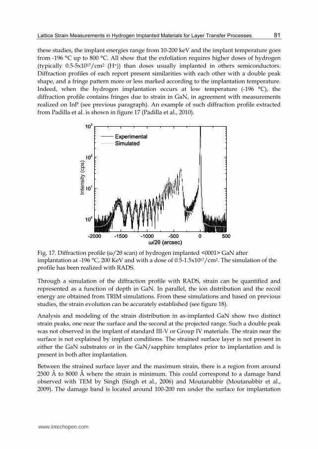
these studies, the implant energies range from 10-200 keV and the implant temperature goes from -196 °C up to 800 °C. All show that the exfoliation requires higher doses of hydrogen (typically 0.5-5x10¹⁷/cm2 (H+)) than doses usually implanted in others semiconductors. Diffraction profiles of each report present similarities with each other with a double peak shape, and a fringe pattern more or less marked according to the implantation temperature. Indeed, when the hydrogen implantation occurs at low temperature (-196 °C), the diffraction profile contains fringes due to strain in GaN, in agreement with measurements realized on InP (see previous paragraph). An example of such diffraction profile extracted from Padilla et al. is shown in figure 17 (Padilla et al., 2010).
-2000 -1500 -1000 -500 0 500
100
101
102
103
Experimental Simulated
ω/2θ (arcsec)
Inte
nsi
ty (
cps)
-2000 -1500 -1000 -500 0 500
100
101
102
103
Experimental Simulated
ω/2θ (arcsec)
Inte
nsi
ty (
cps)
Fig. 17. Diffraction profile (ω/2θ scan) of hydrogen implanted <0001> GaN after implantation at -196 °C, 200 KeV and with a dose of 0.5-1.5x10¹⁷/cm2. The simulation of the profile has been realized with RADS.
Through a simulation of the diffraction profile with RADS, strain can be quantified and represented as a function of depth in GaN. In parallel, the ion distribution and the recoil energy are obtained from TRIM simulations. From these simulations and based on previous studies, the strain evolution can be accurately established (see figure 18).
Analysis and modeling of the strain distribution in as-implanted GaN show two distinct strain peaks, one near the surface and the second at the projected range. Such a double peak was not observed in the implant of standard III-V or Group IV materials. The strain near the surface is not explained by implant conditions. The strained surface layer is not present in either the GaN substrates or in the GaN/sapphire templates prior to implantation and is present in both after implantation.
Between the strained surface layer and the maximum strain, there is a region from around 2500 Å to 8000 Å where the strain is minimum. This could correspond to a damage band observed with TEM by Singh (Singh et al., 2006) and Moutanabbir (Moutanabbir et al., 2009). The damage band is located around 100-200 nm under the surface for implantation
www.intechopen.com

Ion Implantation
82
energies between 50-100 KeV. Here the implantation energy used is 200 KeV, which involves a deeper implantation and a possible shift of the damage band to higher depths.
Fig. 18. The strain profile for the simulated diffraction scan in figure 12 is shown along with the energy transferred from the implanted hydrogen to the lattice as a function of depth (recoils) as well as the hydrogen ion distribution.
3.3.4 Strain and recoil energy
Earlier papers about implantation in semiconductor materials have related the measured strain to the energy lost in nuclear collisions FD also called recoil energy (Paine et al., 1987). In this report, authors implanted heavy species into GaAs at 300 keV with relatively low doses. They showed the strain profile is the maximum where the energy loss by nuclear collisions is a maximum, such that
ε┴,max = KFD,max (3)
where is the implant dose in ions/cm2 (or ions/Å2) and K is a constant representing the conversion of the recoil energy to strain. The K term also may be altered by defect migration and recombination that may reduce the strain – for example, by subsequent annealing.
The linear relationship between strain and FD did not extend to higher doses and decreased for a dose greater than 2x1013 cm-2. In the case of exfoliation, there are distinct differences with the earlier studies. First, hydrogen is light and each implanted hydrogen ion loses significant energy due to electronic stopping not included in FD. Second, the doses typically encountered in an exfoliation process are in the 1016-1017 cm-2 range, which is much higher than doses used for heavier ions. To verify if the linear relationship between strain and FD exists also for exfoliation conditions, different semiconductor materials have been hydrogen implanted using the same implantation parameters. XRD measurements have been performed on the implanted wafers and they are presented in figure 19.
www.intechopen.com

Lattice Strain Measurements in Hydrogen Implanted Materials for Layer Transfer Processes
83
-2000 -1500 -1000 -500 0 50010
-6
10-4
10-2
100
102
104
106
108
1010
GaSb (0.6%)
GaAs (1.2%)
InAs (0.7%)
InP (1%)
Si (1.4%)
Inte
nsi
ty (
cps)
/2 (arcsec) Fig. 19. (004) diffraction profiles (ω/2θ scan) of different cubic semiconductors implanted with hydrogen (H2+, dose 2.5x1016 cm-2) at 77 K and 160 keV. The maximum strain values that correspond to the terminal fringe are noted in parentheses.
In parallel, FD has been calculated using TRIM simulation for each semiconductor. For this, the simulation requires the implantation energy and the dose. The results obtained are presented in figure 20, showing the evaluation of FD as a function of the depth in the implanted material. We observe that the evolution of FD is very similar to the strain (see figure 6 for InP), and reach a maximum at 5400 Å versus 5800 Å for the strain.
0 2000 4000 6000 8000 100000.00
0.05
0.10
0.15
FD (
eV
/Å-i
on
)
Depth (Å)
Si GaAs InP InAs GaSb
Fig. 20. Profiles of FD as a function of depth for different semiconductors, obtained by TRIM simulations using the experimental implant parameters in figure 12.
www.intechopen.com

Ion Implantation
84
On the other hand, a linear relationship between the maximum strain and FDmax is shown in figure 21. Also included in figure 14 is the data measured from implanted Si as well as from SiC and GaN.
SiC
SiGaAs
InP
InAs
GaN
GaSb
0.08 0.12 0.16 0.20 0.24
0.5
1.0
1.5
2.0
2.5
3.0
Ma
xim
um s
trai
n (%
)
FDmax
(eV/Å-ion)
SiC
SiGaAs
InP
InAs
GaN
GaSb
0.08 0.12 0.16 0.20 0.24
0.5
1.0
1.5
2.0
2.5
3.0
Ma
xim
um s
trai
n (%
)
FDmax
(eV/Å-ion)
Fig. 21. The relationship between the maximum experimentally determined strain and the maximum recoil energy FD,max determined by TRIM simulation.
This graph demonstrates that, for the hydrogen implant doses and energies typically used for exfoliation and layer transfer, a linear relationship between FD and strain exists. Whereas the earlier studies demonstrated this relationship only for much lower doses and heavier implant species. The observation that a linear relationship exists for high dose hydrogen implantation into these semiconductors indicates that the relatively low level of nuclear stopping associated with implanted hydrogen maintains a low enough level of damage to ignore higher order damage effects (such as amorphization).
A second interesting result is that the linear relationship between strain and FD for a given dose indicates that the K value is the same (or very similar) for all of the implanted materials. This result contradicts earlier results which observed that there are significant (order of magnitude) differences in K for a given implant species into different targets (Paine et al., 1986). Noting that “defect motion, trapping, or recombination mechanisms are the most responsible for the variations of K between (sic) materials”, the implantation at low temperatures effectively prevents significant defect motion, etc., and thus K becomes a more ‘universal’ value. Additionally, even at these high doses, doubling the dose doubles the strain (Hayashi et al., 2006), showing that the linear relationship between dose and strain exists at the high end of exfoliation implant conditions. Si implanted at an even higher dose produces the same strain – dose relationship (Sousbie et al., 2006) – i.e., K holds for those conditions. This result further supports the concept that the quantitative analysis of the implant-induced strain profile is suitable for a wide range of hydrogen-implanted materials used in exfoliation and layer transfer studies.
www.intechopen.com

Lattice Strain Measurements in Hydrogen Implanted Materials for Layer Transfer Processes
85
4. Conclusion
In this chapter, we have discussed the interest of HRXRD analyses in the ion implantation induced material splitting for layer transfer. This process is a combination of direct wafer bonding and ion implantation. First developed for the SOI production, it has recently been adapted to a wide a number of materials such as Ge, III-V semiconductors, SiC, LiBbO3, etc. Thus, thin layers of materials with qualities comparable to bulk materials can be used for different applications. However, the choice of the implantation parameter is crucial to obtain a successful splitting. Therefore, an analysis of the implanted structure prior splitting is a good way to optimize this choice.
HRXRD constitutes a fast and non-destructive technique to obtain a diagnosis of the implanted structure and determine if they are suitable for exfoliation. We have demonstrated that the ion implantation process induces strain and change in crystallographic planes in the target material. Because of this phenomenon, the diffraction profile measured by XRD presents interference fringes called diffraction pattern. The diffraction profile contains information about the strain in the structure accessible via simulation. The simulation of the diffraction profile can be realized manually by resolving the diffraction equations, or with a program named RADS used in this chapter. With both methods, a localisation and a quantification of the strain in the material is obtained.
We have shown that the strain profile evolves during annealing prior splitting, and HRXRD measurements constitute a good way to monitor this evolution. A diagnosis of the structure is obtained providing information about the stage of the process (hydrogen diffusion, platelet formation, etc). This analysis can help to refine the annealing conditions and obtain the exfoliation.
Finally, the strain profile is related to implantation parameters such as the dose and implantation temperature illustrated with the case of InP. The strain profile is also related to the target materials and their mechanical properties as demonstrated through several examples of semiconductor materials. This validates the fact that HRXRD is very sensitive to any changes in the material structure and constitutes a powerful tool in the study of implanted materials.
5. References
Aspar, B., Moriceau, H., Jalaguier, E., Lagahe, C., Soubie, A., Biasse, B., Papon, A.M., Claverie, A., Grisolia, J., Benassayag, G., Letertre, F., Rayssac, O., Barge, T., Maleville, C. & Ghyselen, B. (2001). The generic nature of the Smart-Cut((R)) process for thin film transfer. Journal of Electronic Materials, Vol.30, No.7, (July 2001), pp. 834-840, ISSN 0361-5235
Balboni, R., Milita, S. and Servidori, M. (1995). On the role of the static Debye-Waller factor in X-Ray rocking curve analysis. Physica Status Solidi A-Applied Research, Vol.148, No.1, (March 1995), pp. 95-105, ISSN 0031-8965
Bruel, M. (1995). Silicon on insulator material technology. Electronics letters, Vol.31, No.14, (July 1995), pp. 1201-1202, ISSN 0013-5194
www.intechopen.com

Ion Implantation
86
Cembali, F., Servidori, M. & Zani, A. (1985). Double crystal X-Ray difraction analysis of low temperature ion-implanted silicon. Solid-State Electronics, Vol.28, No.9, (1985), pp. 933-943, ISSN 0038-1101
Chu, W.K., Kastl, R.H., Lever, R.F., Mader, S. & Masters, B.J. (1997). Distribution of irradiation damage in silicon bombarded with hydrogen. Physical Review B, Vol.16, No.9, (May 1977), pp. 3851-3859, ISSN 0163-1829
Colinge, C.A, Byun, K.Y., Ferain, I.P., Yu, R. and Goorsky, M.S. (2011). Low-temperature fabrication of germanium-on-insulator using remote plasma activation bonding and hydrogen exfoliation, In: Semiconductor-on-insulator materials for nanoelectronics applications, A. Zanarov, J.-P. Colinge, F. Balestra, J.-P. Raskin, F. Gamiz, V.S. Lysenko, pp. 31-46, SpringerLink
Duo, X., Liu, W.L., Zhang, M., Wang, L.W., Lin, C.L., Okuyama, M., Noda, M., Cheung, W.-Y., Wong, S.P., Chu, P.K., Hu, P.G., Wang, S.X. and Wang, L.M. (2001). Evolution of hydrogen and helium co-implanted single-crystal silicon during annealing. Journal of Applied Physics, Vol.90, No.8, (October 2001), pp. 3780-3786, ISSN 0021-8979
Ferain, I.P., Byun, K.Y., Colinge, C.A., Brightup, S. & Goorsky, M.S. (2010). Low temperature exfoliation process in hydrogen-implanted germanium layers. Journal of Applied Physics, Vol.107, No.5, (March 2010), pp. 054315-1-054315-5, ISSN 0021-8979
Grisolia, J., Ben Assayag, G., Claverie, A., Aspar, B., Lagahe, C. & Laanab, L. (2000). A transmission electron microscopy quantitative study of the growth kinetics of H platelets in Si. Applied Physics Letters, Vol.76, No.7, (February 2000), pp. 852-854, ISSN 0003-6951
Hayashi, S., Poust, B., Heying, B. & Goorsky, M.S. (2003). Exfoliation of GaN layers using hydrogen implantation, Proceedings of Compound Semiconductors 2003, International Symposium, ISSN 0-7803-7820-2, San Diego, August 2003
Hayashi, S., Bruno, D. & Goorsky, M.S. (2004). Temperature dependence of hydrogen-induced exfoliation of InP. Applied Physics Letters, Vol.85, No.2, (July 2004), pp. 236-238, ISSN 0003-6951
Hayashi, S., Goorsky, M.S., Noori, A. & Bruno, D. (2006). Materials issues for the heterogeneous integration of III-V compounds. Journal of the Electrochemical Society, Vol.153, No.12, (October 2006), pp. G1011-G1014, ISSN 0013-4651
Höchbauer, T., Nastasi, M. & Mayer, J.W. (1999). Hydrogen blister depth in boron and hydrogen coimplanted n-type silicon. Applied Physics Letters, Vol.75, No.25, (December 1999), pp. 3938-3940, ISSN 0003-6951
Höchbauer, T., Misra, A., Nastasi, M. & Mayer, J.W. (2001). Investigation of the cut location in hydrogen implantation induced silicon surface exfoliation. Journal of Applied Physics, Vol.89, pp. 5980-5990 ISSN 0021-8979
Horng, S.T., Goorsky, M.S., Madok, J.H. & Haegel, N.M. (1994). Strain and mosaic spread of carbon and gallium co-implanted GaAs. Journal of Applied Physics, Vol.76, No.4, pp. 2066-2069 ISSN 0021-8979
Kyutt, R.N., Petrashen, P.V. & and Sorokin, L.M. (1980). Strain profiles in ion-doped silicon obtained from X-Ray rocking curve. Physica Status Solidi A-Applied Research, Vol.60, No.2, (1980), pp. 381-389, ISSN 0031-8965
Larson, B.C. and Barhost, J.F. (1980). X-Ray study of lattice strain in boron implanted laser annealed silicon. Journal of Applied Physics, Vol.51, No.6, (1980), pp. 3181-3185, ISSN 0021-8979
www.intechopen.com

Lattice Strain Measurements in Hydrogen Implanted Materials for Layer Transfer Processes
87
Malouf, G., Poust, B., Hayashi, S., Yoshizawa, G. & Goorsky, M.S. (2005). Hydrogen-induced blistering of SiC: the role of post-implant multi-step annealing sequences. Materials Science Forum, Vol.527-529, (October 2006), pp. 855-858, ISSN 1662-9752
Meda, L., Cerofolini, G.F., Dierckx, R., Mercurio, G., Servidori, M., Cembali, F., Anderle, M., Canteri, R., Ottaviani, G., Claeys, C. & Vanhellemont, J. (1989). Hydrogen implantation into (100) silicon – A study of the released damage. Nuclear Instruments & Methods in Physics Research section B-beam interaction with materials and atoms, Vol.39, No.1-4, (March 1989), pp. 381-385, ISSN 0168-583X
Moutanabbir, O., Chabal, Y.J., Chicoine, M., Christiansen, S., Krause-Rehberg, R., Schiettekatte, F., Scholz, R., Seitz, O., Süßkraut, F. & Gösele, U. (2009). Mechanisms of ion-induced GaN thin layer splitting. Nuclear Instruments & Methods in Physics Research B, Vol.267, pp. 1264-1268
Nastasi, M., Höchbauer, T., Lee, J.K., Misra, A., Hirth, J.P., Ridgway, M. & Lafford, T. (2005). Nucleation and growth of platelets in hydrogen-ion-implanted silicon. Applied Physics Letters, Vol.86, No.15, (April 2005), pp. 154102, ISSN 0003-6951
Padilla, E., Jackson, M. and Goorsky, M.S. (2010). The role of the nucleation annealing temperature annealing on the exfoliation of hydrogen-implanted GaN, Proceedings of Semiconductor wafer bonding 11: Science, Technology and Applications, ISBN 978-1-56677-823, Las Vegas, October 2010.
Paine, B.M., Hurvitz, N.N. and Speriosu, V.S. (1987). Strain in GaAs by low-dose ion implantation. Journal of Applied Physics, Vol.61, No.4, (February 1987), pp. 1335-1339, ISSN 0021-8979
Radu, I., Szafraniak, I., Scholz, R., Alexe, M. & Gösele, U. (2002). Blistering and exfoliation of hydrogen and helium implanted (100) GaAs, Proceedings of International Semiconductor Conference, 0-7803-7440-1, Romania, October, 2002.
Reboh, S., Schaurich, F., Declemy, A., Barbot, J.F., Beaufort, M.F., Cherkashin, N. and Fichtner, P.F.P. (2010). On the microstructure of Si coimplanted with H+ and He+
ions at moderate energies. Journal of Applied Physics, Vol.108, No.2, (July 2010), pp. 023502-1-023502-6, ISSN 0021-8979
Servidori, M. (1987). Characterization of lattice damage in ion implanted silicon by multiple crystal X-Ray diffraction. Nuclear Instruments & Methods in Physics Research section B-beam interaction with materials and atoms, Vol.19-2, (February 1987), pp. 443-449, ISSN 0168-583X
Singh, R., Radu, I., Gösele, U. & Christiansen, S.H. (2006). Investigation of hydrogen implantation induced blistering in GaN. Physica Status Solidi, Vol.3, No.6, pp. 1754-1757
Speriosu, V.S. (1981). Kinematical X-Ray diffraction in nonuniform crystalline films: strain and ion distributions in-ion implanted garnets. (1981). Journal of Applied Physics, Vol.52, No.10, (1981), pp. 6094-6103, ISSN 0021-8979
Speriosu, V.S., Paine, B.M. & Nicolet, M-A. (1982). X-Ray rocking study of Si-implanted GaAs, Si and Ge. Applied Physics Letters, Vol.40, No.7, (1982), pp. 604-606, ISSN 0003-6951
Sousbie, N., Capello, L., Eymery, J., Rieutord, F. and Lagahe, C. (2006). X-Ray scattering study of hydrogen implantation in silicon. Journal of Applied Physics, Vol.99, No.11, (May 2006), pp. 103509-1-103509-7, ISSN 0021-8979
Taupin, D. (1964). The dynamic theory of the diffraction of X-Rays by deformed crystals. Bulletin de la Societe Francaise de Mineralogie et de Cristallographie, Vol.88, No.4, pp. 469-511
www.intechopen.com

Ion Implantation
88
Tauzin, A., Akatsu, T., Rabarot, M., Dechamp, J., Zussy, M., Moriceau, H., Michaud, J.-F., Charvet, A.-M., Di Cioccio, L., Fournel, F., Garrione, J., Faure, B., Letertre, F. & Kernevez, N. (2005). Transfers of 2-inch GaN films on sapphire substrates using Smart Cut™ technology. Electronics Letters, Vol.41, No.11, pp. 668-670, ISSN 0013-5194
Tong, Q.-Y., Chao, Y.-L., Huang, L.-J. & Gösele, U. (1999). Low temperature InP layer transfer. Electronics Letters, Vol.35, No.4, pp. 341-342, ISSN 0013-5194
Ventosa-Moulet, C., Hayashi, S.L. and Goorsky, M.S. (2010). Lattice strain and strain evolution in hydrogen implanted materials: the role of mechanical properties and hydrogen diffusion, Proceedings of Semiconductor wafer bonding 11: Science, Technology and Applications, ISBN 978-1-56677-823, Las Vegas, October 2010.
Weldon, M.K., Marsico, V.E., Chabal, Y.J., Agarwal, A., Eaglesham, D.J., Sapjeta, J., Brown, W.L., Jacobson, D.C., Caudano, Y., Christman, S.B. & Chaban, E.E. (1997). On the mechanism of the hydrogen-induced exfoliation of silicon. Journal of Vacuum Science & Technology B, Vol.15, No.4, (July August 1997), pp. 1065-1073, IDS XT088
Wie, C.R., Tombrello, T.A. & Vreeland, T. (1986). Dynamical X-Ray diffraction from non uniform crystalline films: application to X-Ray rocking curve analysis. Journal of Applied Physics, Vol.59, No.11, (June 1986), pp. 3743-3746, ISSN 0021-8979
Zahler, J.M., Morral, A.F.I., Griggs, M.J. Atwater, H.A. & Chabal, Y.J. (2007). Role of hydrogen in hydrogen-induced layer exfoliation of germanium. Physical Review B, Vol.75, No.3, (January 2007), pp. 035309-1-035309-10, ISSN 1098-0121
Ziegler, J.F. (1985). The stopping and range of ions in solids, TarryTown, ISBN 008021603X, New York, USA
www.intechopen.com

Ion ImplantationEdited by Prof. Mark Goorsky
ISBN 978-953-51-0634-0Hard cover, 436 pagesPublisher InTechPublished online 30, May, 2012Published in print edition May, 2012
InTech EuropeUniversity Campus STeP Ri Slavka Krautzeka 83/A 51000 Rijeka, Croatia Phone: +385 (51) 770 447 Fax: +385 (51) 686 166www.intechopen.com
InTech ChinaUnit 405, Office Block, Hotel Equatorial Shanghai No.65, Yan An Road (West), Shanghai, 200040, China
Phone: +86-21-62489820 Fax: +86-21-62489821
Ion implantation presents a continuously evolving technology. While the benefits of ion implantation are wellrecognized for many commercial endeavors, there have been recent developments in this field. Improvementsin equipment, understanding of beam-solid interactions, applications to new materials, improvedcharacterization techniques, and more recent developments to use implantation for nanostructure formationpoint to new directions for ion implantation and are presented in this book.
How to referenceIn order to correctly reference this scholarly work, feel free to copy and paste the following:
Caroline Moulet and Mark. S. Goorsky (2012). Lattice Strain Measurements in Hydrogen Implanted Materialsfor Layer Transfer Processes, Ion Implantation, Prof. Mark Goorsky (Ed.), ISBN: 978-953-51-0634-0, InTech,Available from: http://www.intechopen.com/books/ion-implantation/lattice-strain-measurements-in-hydrogen-implanted-materials-for-layer-transfer-processes

© 2012 The Author(s). Licensee IntechOpen. This is an open access articledistributed under the terms of the Creative Commons Attribution 3.0License, which permits unrestricted use, distribution, and reproduction inany medium, provided the original work is properly cited.