Embed Size (px)
Citation preview

LBI-38760
Printed in U.S.A.
MAINTENANCE MANUALMAIN BOARD ASSEMBLY
N29/85154001220 440-470 MHzN29/85154001250 470-512 MHz
TABLE OF CONTENTSPage
DESCRIPTION . . . . . . . . . . . . . . . . . . . . . . . . . . . . . . . . . . . . . . . . . . . . . . Front Cover
CIRCUIT ANALYSIS . . . . . . . . . . . . . . . . . . . . . . . . . . . . . . . . . . . . . . . . . . . Front Cover
AUDIO CIRCUIT . . . . . . . . . . . . . . . . . . . . . . . . . . . . . . . . . . . . . . . . . . Front Cover
LOGIC CIRCUIT . . . . . . . . . . . . . . . . . . . . . . . . . . . . . . . . . . . . . . . . . . . 2
SYNTHESIZER CIRCUIT . . . . . . . . . . . . . . . . . . . . . . . . . . . . . . . . . . . . . . 2
RECEIVER CIRCUIT . . . . . . . . . . . . . . . . . . . . . . . . . . . . . . . . . . . . . . . . 4
TRANSMITTER CIRCUIT . . . . . . . . . . . . . . . . . . . . . . . . . . . . . . . . . . . . . 7
POWER DISTRIBUTION . . . . . . . . . . . . . . . . . . . . . . . . . . . . . . . . . . . . . . 7
SERVICE NOTES . . . . . . . . . . . . . . . . . . . . . . . . . . . . . . . . . . . . . . . . . . . . . 7
AUDIO CIRCUIT . . . . . . . . . . . . . . . . . . . . . . . . . . . . . . . . . . . . . . . . . . 7
LOGIC CIRCUIT . . . . . . . . . . . . . . . . . . . . . . . . . . . . . . . . . . . . . . . . . . . 7
SYNTHESIZER CIRCUIT . . . . . . . . . . . . . . . . . . . . . . . . . . . . . . . . . . . . . . 8
TRANSMITTER CIRCUIT . . . . . . . . . . . . . . . . . . . . . . . . . . . . . . . . . . . . . 8
RECEIVER CIRCUIT . . . . . . . . . . . . . . . . . . . . . . . . . . . . . . . . . . . . . . . . 8
OUTLINE DIAGRAM . . . . . . . . . . . . . . . . . . . . . . . . . . . . . . . . . . . . . . . . . . 9
SCHEMATIC DIAGRAM . . . . . . . . . . . . . . . . . . . . . . . . . . . . . . . . . . . . . . . . 10
IC DATA . . . . . . . . . . . . . . . . . . . . . . . . . . . . . . . . . . . . . . . . . . . . . . . . . . 15
PARTS LIST . . . . . . . . . . . . . . . . . . . . . . . . . . . . . . . . . . . . . . . . . . . . . . . . 19
DESCRIPTION
The Main Board performs most of the radio’s functions.It is divided into two sections by a partition in the aluminumcasting. The audio, logic and system circuitry are located inone section, near the front of the radio. The RF Circuitincluding the synthesizer, exciter and power control circuitof the transmitter are located in the other section, near theback of the radio.
CIRCUIT ANALYSIS
AUDIO CIRCUIT
The audio circuit is located on the front section of theMain Board and on the same side as the display. The audiocircuit provides all audio and tone processing for the receiverand transmitter. The audio circuit obtains all control signalsfrom the logic circuit and interconnects with the MICthrough an 8 pin RJ connector (J5). The audio circuit con-tains 4 main paths: a receiver audio path, a tone path, atransmitter audio path, and a receiver squelch path.
SYMBOL PART NUMBER DESCRIPTION
— — — TRANSFORMERS — — —
T1 Balun, 7 mm sq.andT2
— — — MISCELLANEOUS — — —
Brass pin.
Top Cover, Front End.
Bottom Cover, Front End.
Frame, Front End.
DBM cover.
VC2 N29/SMR08 RECEIVER IF Module.
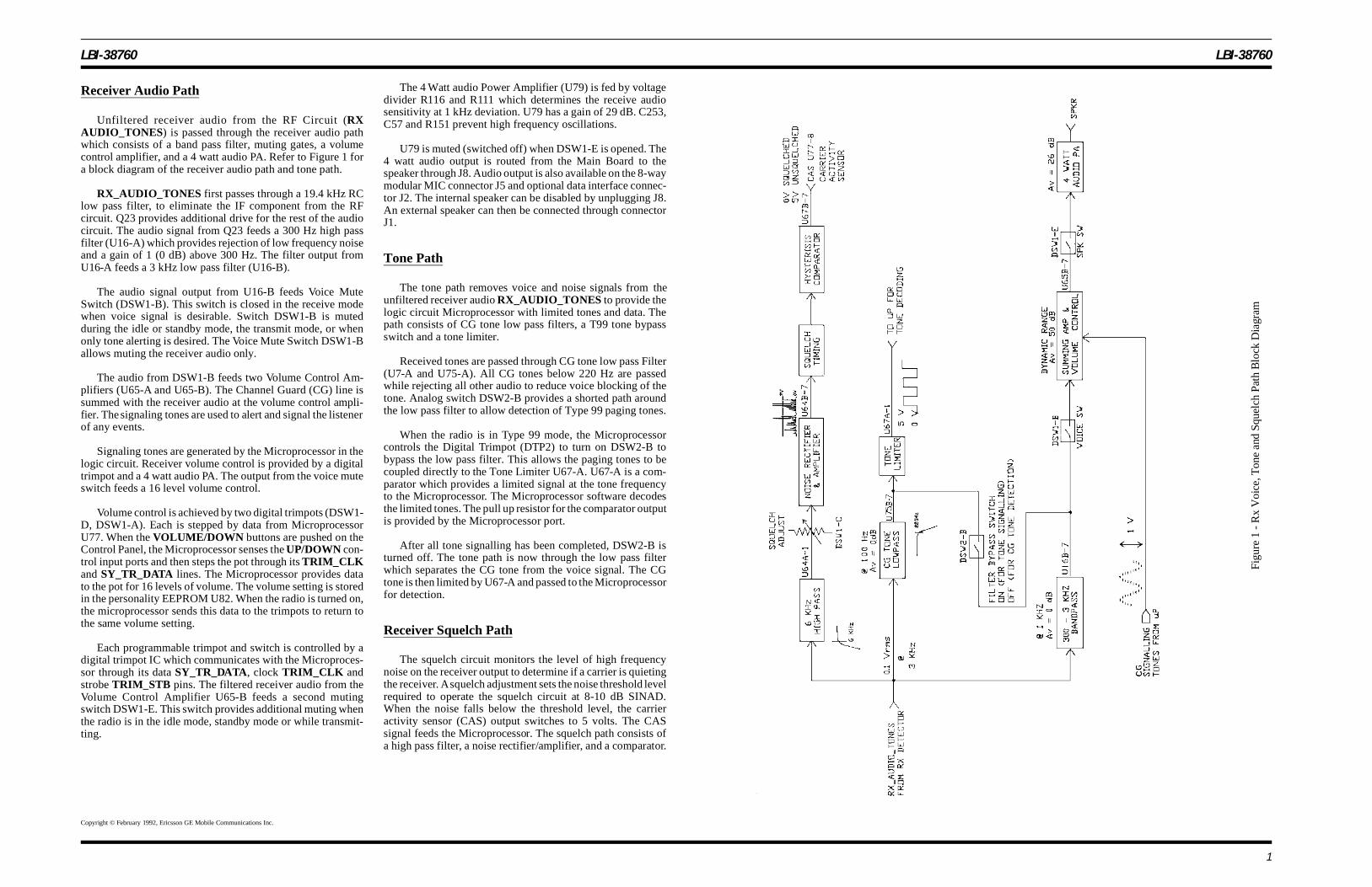
Receiver Audio Path
Unfiltered receiver audio from the RF Circuit (RXAUDIO_TONES) is passed through the receiver audio pathwhich consists of a band pass filter, muting gates, a volumecontrol amplifier, and a 4 watt audio PA. Refer to Figure 1 fora block diagram of the receiver audio path and tone path.
RX_AUDIO_TONES first passes through a 19.4 kHz RClow pass filter, to eliminate the IF component from the RFcircuit. Q23 provides additional drive for the rest of the audiocircuit. The audio signal from Q23 feeds a 300 Hz high passfilter (U16-A) which provides rejection of low frequency noiseand a gain of 1 (0 dB) above 300 Hz. The filter output fromU16-A feeds a 3 kHz low pass filter (U16-B).
The audio signal output from U16-B feeds Voice MuteSwitch (DSW1-B). This switch is closed in the receive modewhen voice signal is desirable. Switch DSW1-B is mutedduring the idle or standby mode, the transmit mode, or whenonly tone alerting is desired. The Voice Mute Switch DSW1-Ballows muting the receiver audio only.
The audio from DSW1-B feeds two Volume Control Am-plifiers (U65-A and U65-B). The Channel Guard (CG) line issummed with the receiver audio at the volume control ampli-fier. The signaling tones are used to alert and signal the listenerof any events.
Signaling tones are generated by the Microprocessor in thelogic circuit. Receiver volume control is provided by a digitaltrimpot and a 4 watt audio PA. The output from the voice muteswitch feeds a 16 level volume control.
Volume control is achieved by two digital trimpots (DSW1-D, DSW1-A). Each is stepped by data from MicroprocessorU77. When the VOLUME/DOWN buttons are pushed on theControl Panel, the Microprocessor senses the UP/DOWN con-trol input ports and then steps the pot through its TRIM_CLKand SY_TR_DATA lines. The Microprocessor provides datato the pot for 16 levels of volume. The volume setting is storedin the personality EEPROM U82. When the radio is turned on,the microprocessor sends this data to the trimpots to return tothe same volume setting.
Each programmable trimpot and switch is controlled by adigital trimpot IC which communicates with the Microproces-sor through its data SY_TR_DATA, clock TRIM_CLK andstrobe TRIM_STB pins. The filtered receiver audio from theVolume Control Amplifier U65-B feeds a second mutingswitch DSW1-E. This switch provides additional muting whenthe radio is in the idle mode, standby mode or while transmit-ting.
The 4 Watt audio Power Amplifier (U79) is fed by voltagedivider R116 and R111 which determines the receive audiosensitivity at 1 kHz deviation. U79 has a gain of 29 dB. C253,C57 and R151 prevent high frequency oscillations.
U79 is muted (switched off) when DSW1-E is opened. The4 watt audio output is routed from the Main Board to thespeaker through J8. Audio output is also available on the 8-waymodular MIC connector J5 and optional data interface connec-tor J2. The internal speaker can be disabled by unplugging J8.An external speaker can then be connected through connectorJ1.
Tone Path
The tone path removes voice and noise signals from theunfiltered receiver audio RX_AUDIO_TONES to provide thelogic circuit Microprocessor with limited tones and data. Thepath consists of CG tone low pass filters, a T99 tone bypassswitch and a tone limiter.
Received tones are passed through CG tone low pass Filter(U7-A and U75-A). All CG tones below 220 Hz are passedwhile rejecting all other audio to reduce voice blocking of thetone. Analog switch DSW2-B provides a shorted path aroundthe low pass filter to allow detection of Type 99 paging tones.
When the radio is in Type 99 mode, the Microprocessorcontrols the Digital Trimpot (DTP2) to turn on DSW2-B tobypass the low pass filter. This allows the paging tones to becoupled directly to the Tone Limiter U67-A. U67-A is a com-parator which provides a limited signal at the tone frequencyto the Microprocessor. The Microprocessor software decodesthe limited tones. The pull up resistor for the comparator outputis provided by the Microprocessor port.
After all tone signalling has been completed, DSW2-B isturned off. The tone path is now through the low pass filterwhich separates the CG tone from the voice signal. The CGtone is then limited by U67-A and passed to the Microprocessorfor detection.
Receiver Squelch Path
The squelch circuit monitors the level of high frequencynoise on the receiver output to determine if a carrier is quietingthe receiver. A squelch adjustment sets the noise threshold levelrequired to operate the squelch circuit at 8-10 dB SINAD.When the noise falls below the threshold level, the carrieractivity sensor (CAS) output switches to 5 volts. The CASsignal feeds the Microprocessor. The squelch path consists ofa high pass filter, a noise rectifier/amplifier, and a comparator.
Copyright © February 1992, Ericsson GE Mobile Communications Inc.
Figu
re 1
- R
x V
oice
, Ton
e an
d Sq
uelc
h Pa
th B
lock
Dia
gram
LBI-38760 LBI-38760
1
RX_AUDIO_TONES is the unfiltered receiver audiooutput from the RF circuit. A 6 kHz High Pass Filter (U64-A)removes all voice signals from the RX_AUDIO_TONEoutput. The filter provides a gain of 8 dB at 8-10 kHz anddrops 3 dB at the 6 kHz cutoff frequency.
Noise in the 6-8 kHz range is coupled to the SquelchAdjust DSW1-C, which varies the level of noise to the noiseRectifier/Amplifier U64-B. U64-B is biased at ground, am-plifying only the positive peaks of the noise by about 9 dB.
The rectified noise is filtered by R95 and C21 to providean average DC level proportional to the noise level. This DClevel is applied to the inverting (-) of Comparator U67-B.The non-inverting input (+) of U67-B is referenced to 90 mV.
When the DC noise level falls below 90 mV DC, thecomparator output switches the CAS line to +5 Volts to tellthe Microprocessor the channel is busy with a carrier. Thecomparator output will remain at a logic high until the DCnoise level exceeds 120 mV. This difference in voltagebetween the CAS turn-on and turn-off points provides suffi-cient hysteresis to eliminate "bubbling" or chattering noisefrom the speaker. The "bubbling" would normally be causedby transitional changes in the DC level around the referencepoint. The hysteresis is provided by R142.
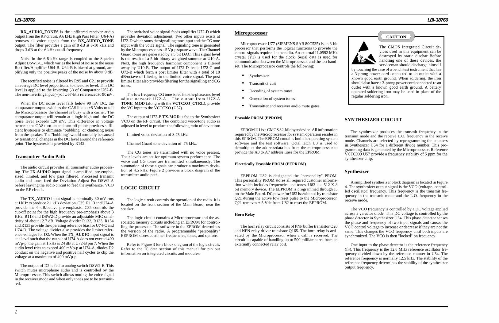
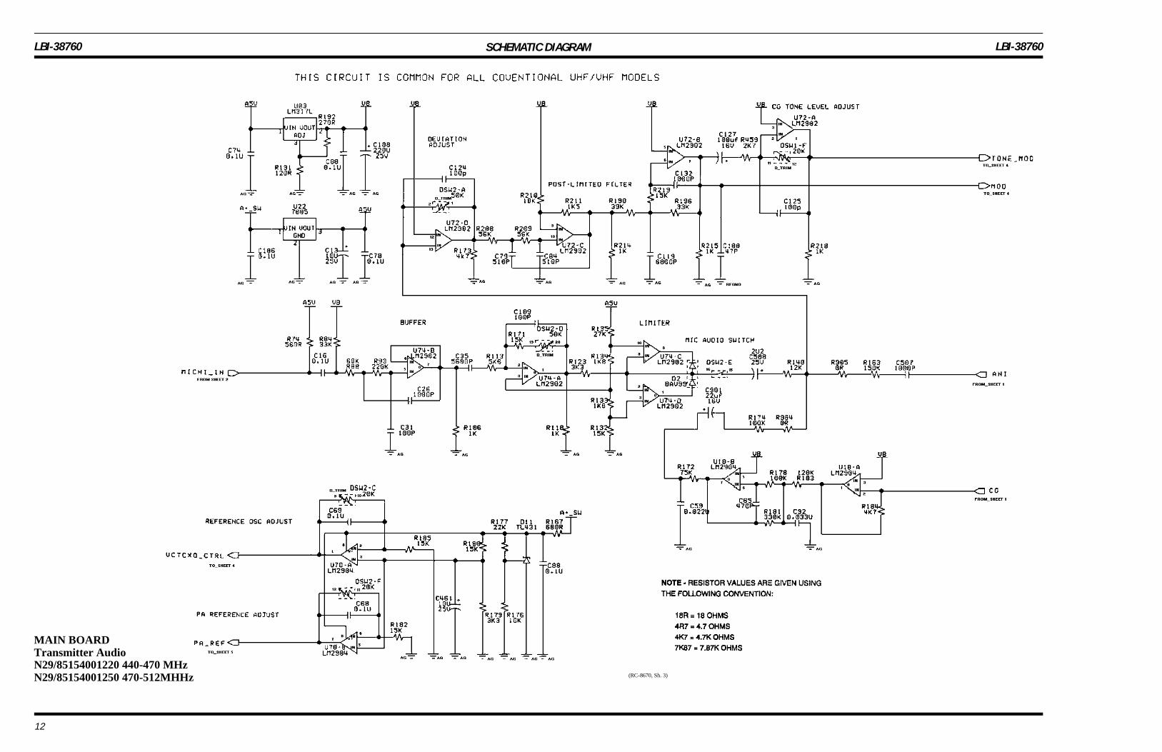
Transmitter Audio Path
The audio circuit provides all transmitter audio process-ing. The TX-AUDIO input signal is amplified, pre-empha-sized, limited, and low pass filtered. Processed transmitaudio and tones feed the Deviation Adjust Pot DSW2-Abefore leaving the audio circuit to feed the synthesizer VCOon the RF circuit.
The TX_AUDIO input signal is nominally 80 mV rmsat 1 kHz to produce 2.1 kHz deviation. C35, R113 and U74-Aprovide the 6 dB/octave pre-emphasis. C35 controls thecut-off point for the high frequency pre-emphasis above 3KHz. R113 and DSW2-D provide an adjustable MIC sensi-tivity of about 12.7 dB. Voltage divider R132, R133, R134and R135 provide the operating reference bias for U74-C andU74-D. The voltage divider also provides the limiter refer-ence voltages for D2. When the TX_AUDIO input signal isat a level such that the output of U74-A does not exceed 400mVp-p, the gain at 1 kHz is 24 dB at U72-B pin 7. When theaudio level tries to exceed 400 mVp-p at U74-A, diodes D2conduct on the negative and positive half cycles to clip thevoltage at a maximum of 400 mVp-p.
The output of D2 is fed to analog switch DSW2-E. Thisswitch mutes microphone audio and is controlled by theMicroprocessor. This switch allows muting the voice signalin the receiver mode and when only tones are to be transmit-ted.
The switched voice signal feeds amplifier U72-D whichprovides deviation adjustment. Two other inputs exists atU72-D which sums the signalling tone input and the CG toneinput with the voice signal. The signaling tone is generatedby the Microprocessor as a 5 Vp-p square wave. The ChannelGuard tones are generated by a 5 bit DAC. This signal levelis the result of a 5 bit binary weighted summer at U10-A.Next, the high frequency harmonic component is filteredaway by U10-B. The output of U72-D feeds U72-C andU72-B which form a post limiter filter with a total of 18dB/octave of filtering to the limited voice signal. The postlimiter filter also provides filtering for the signalling and CGtones.
The low frequency CG tone is fed into the phase and leveladjust network U72-A. The output from U72-ATONE_MOD (along with the VCTCXO_CTRL ), providethe VC input to the VCTCXO (U57).
The output of U72-B TX-MOD is fed to the SynthesizerVCO on the RF circuit. The combined voice/tone audio isadjusted in level to produce the following ratio of deviation:
Limited voice deviation of 3.75 kHz
Channel Guard tone deviation of .75 kHz.
The CG tones are transmitted with no voice present.Their levels are set for optimum system performance. Thevoice and CG tones are transmitted simultaneously. Thesummation of these signals can produce a maximum devia-tion of 4.5 kHz. Figure 2 provides a block diagram of thetransmitter audio path.
LOGIC CIRCUIT
The logic circuit controls the operation of the radio. It islocated on the front section of the Main Board, near thespeaker.
The logic circuit contains a Microprocessor and the as-sociated memory circuits including an EPROM for control-ling the processor. The software in the EPROM determinesthe version of the radio. A programmable "personality"EEPROM stores customer frequencies, tones, and options.
Refer to Figure 3 for a block diagram of the logic circuit.Refer to the IC data section of this manual for pin outinformation on integrated circuits and modules.
Microprocessor
Microprocessor U77 (SIEMENS SAB 80C535) is an 8-bitprocessor that performs the logical functions to provide thecontrol signals required in the radio. An external 11.0592 MHzcrystal (Y1) is used for the clock. Serial data is used forcommunication between the Microprocessor and the test hand-set. The Microprocessor controls the following:
• Synthesizer
• Transmit circuit
• Decoding of system tones
• Generation of system tones
• Transmitter and receiver audio mute gates
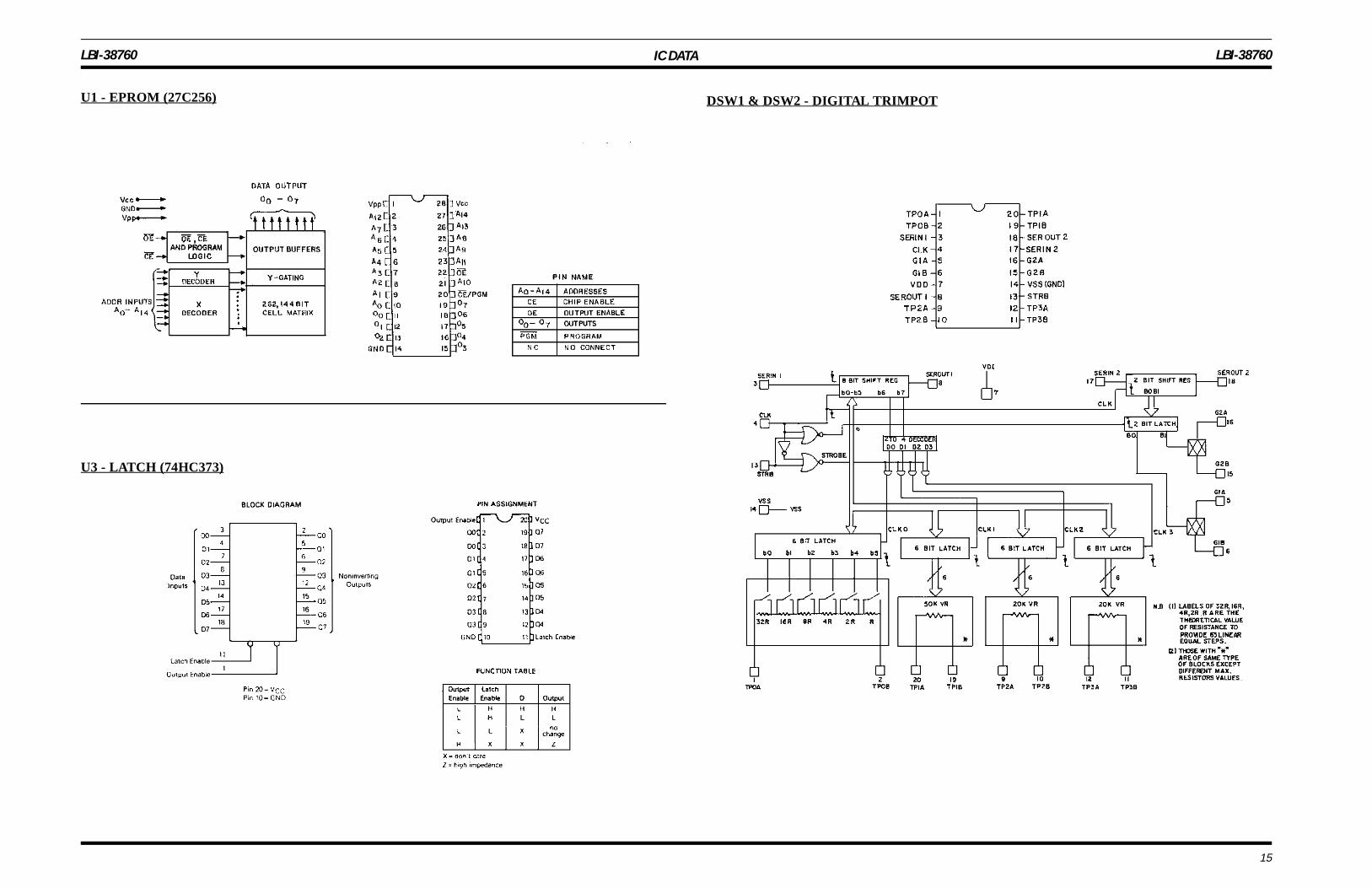
Erasable PROM (EPROM)
EPROM U1 is a CMOS 32-kilobyte device. All informationrequired by the Microprocessor for system operation resides inthis EPROM. The EPROM contains both the operating systemsoftware and the test software. Octal latch U3 is used todemultiplex the address/data bus from the microprocessor toprovide the A0 to A7 address lines for the EPROM.
Electrically Erasable PROM (EEPROM)
EEPROM U82 is designated the "personality" PROM.This personality PROM stores all required customer informa-tion which includes frequencies and tones. U82 is a 512 X 8bit memory device. The EEPROM is programmed through J5on the Main Board. DC power for U82 is switched by transistorQ21 during the active low reset pulse to the Microprocessor.Q21 removes + 5 Vdc from U82 to reset the EEPROM.
Horn Relay
The horn relay circuit consists of PNP buffer transistor Q20and NPN relay driver transistor Q165. The horn relay is acti-vated by the Microprocessor when a call is received. Thecircuit is capable of handling up to 500 milliamperes from anexternally connected relay coil.
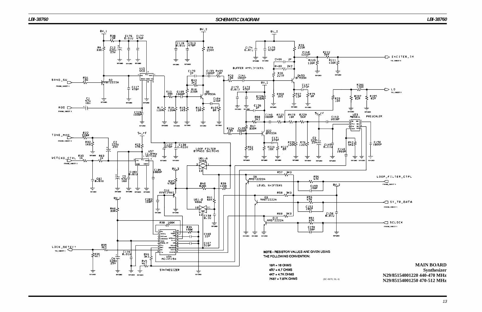
SYNTHESIZER CIRCUIT
The synthesizer produces the transmit frequency in thetransmit mode and the receive L.O. frequency in the receivemode. Channels are selected by reprogramming the countersin Synthesizer U54 for a different divide number. This pro-gramming data is generated by the Microprocessor. ReferenceVCTCXO U57 provide a frequency stability of 5 ppm for thesynthesizer chip.
Synthesizer
A simplified synthesizer block diagram is located in Figure4. The synthesizer output signal is the VCO (voltage- control-led oscillator) frequency. This frequency is the transmit fre-quency in the transmit mode and the L.O. frequency in thereceive mode.
The VCO frequency is controlled by a DC voltage appliedacross a varactor diode. This DC voltage is controlled by thephase detector in Synthesizer U54. This phase detector sensesthe phase and frequency of two input signals and causes theVCO control voltage to increase or decrease if they are not thesame. This changes the VCO frequency until both inputs aresynchronized. The VCO is then "locked" on frequency.
One input to the phase detector is the reference frequency(fR). This frequency is the 12.8 MHz reference oscillator fre-quency divided down by the reference counter in U54. Thereference frequency is normally 12.5 kHz. The stability of thereference frequency determines the stability of the synthesizeroutput frequency.
The CMOS Integrated Circuit de-vices used in this equipment can bedestroyed by static dischar Beforehandling one of these devices, theserviceman should discharge himself
by touching the case of a bench test instrument that hasa 3-prong power cord connected to an outlet with aknown good earth ground. When soldering, the ironshould also have a 3-prong power cord connected to anoutlet with a known good earth ground. A batteryoperated soldering iron may be used in place of theregular soldering iron.
CAUTION
LBI-38760 LBI-38760
2
Fig
ure
2 -
TX
Aud
io B
lock
Dia
gram
Fig
ure
3 -
Log
ic C
ircu
it B
lock
Dia
gra
m
LBI-38760 LBI-38760
3

The reference VCTCXO U57 is temperature compensatedto provide a frequency stability of ±5ppm from -30 to + 80degrees °C. The reference frequency can also be finely trimmedby a DC voltage applied to the VC input of the VCTCXO.
The other input to the phase detector (fV) is derived fromthe VCO signal. The VCO frequency is divided down byPrescaler U53 and by the N counter in U54. These counters areprogrammed for each channel to divide by a number. This willresult in an input to the phase detector that is the same as thereference frequency when the VCO is operating on the correctfrequency. Note that the VCO, prescaler, N counter, and thephase detector form a loop. Therefore, if any component in thisloop is defective, improper signals appear throughout the loop.
VCO U15
The VCO frequency is controlled by changing the DCvoltage applied across a varactor diode inside. As the DCvoltage across a varactor increases, the capacitance of the diodedecreases and vice versa. This causes the VCO frequency toincrease as the control voltage increases.
The VCO is frequency modulated in a similar manner. Thetransmit audio signal is applied across another varactor diodeto vary the VCO frequency at an audio rate. A compensationnetwork is used to ensure that modulation remains constantover the entire frequency band of the VCO. This compensationis required be-cause modulation tends to increase as VCOfrequency gets higher.
The resonant frequency of the tank circuit is decreased inthe receive mode by approximately 45 MHz. It is achieved byswitching in additional capacitance by means of a pin diode.This is done to keep the VCO control voltage in the middle ofits range.
Injection Chain
The VCO signal is attenuated by a pad formed by R17, R13,and R14 before being coupled to amplifier Q6. The amplifiedsignal is divided and applied to two other amplifiers Q459 andQ22. Output from amplifier Q459 is attenuated by R220, R222and R221 to drive the Exciter Module. Output from amplifierQ22 is divided into two separate paths. One path goes to a padformed by R226, R229, and R76 and then drives Prescaler U53.The other path provides the L.O. signal for the Front-EndModule after attenuated by R207, R206, and R205.
Prescaler U53
The prescaler is hardware set to divide by 128/129. Thedivision ratio is controlled by a logic signal at pin 6, theMODULUS CONTROL input from synthesizer IC U54. U53
divides by 128 when the control input from the synthesizer ishigh and by 129 when the control input is low.
Adaptive Loop Filter
The loop filter consists of C137, C138, C139, R39, R40,R41. This low pass filter controls synthesizer stability, lockuptime and suppresses the loop reference frequency (fR). AnalogSwitches U61-A and U61-D are used to bypass the resistancein the loop filter to speed up the lockup time. These switchesare enabled for about 5 ms whenever the synthesizer chip isreprogrammed. A logic high closes the switch and a low logicopens the switch.
The VCO frequency is controlled by a DC voltage filteredby the loop filter. The input signal to the loop filter is the APD(analog phase detector) output of U54.
This output is from a sample and hold circuit which pro-duces a voltage proportional to the phase difference betweenthe fV and fR signals. If the phase of fV lags that of fR, the APDoutput ramps up between the time the fV and fR pulses occur.Conversely, if fV leads fR, the APD output ramps down duringthis period. The greater the phase difference, the more the rampvoltage increases or decreases before it holds. When the syn-thesizer is far out of lock such as when the channel is changed,the VCO is swept into lock by pulses, occurring at a rate equalto the frequency difference between fR and fV.
Buffer Q16 provides a low impedance output to the loopfilter. This isolates the high impedance output of the APDoutput so that it does not affect the roll off characteristics ofthe filter. Q16 also improves the current drive capability of theAPD output which results in a faster lockup time.
RECEIVER CIRCUIT
The double conversion receiver circuit consists of a frontend module, a 45 MHz IF module and a receive switch. Bothmodules are shielded to prevent interference to their sensitivecircuits. See Figure 6, on page 6, for a block diagram of theReceiver section.
Fig
ure
4 -
Syn
thes
ize
r B
lock
Dia
gram
The following circuit analysis for the Front End Module(VC1), references components found in Figure 5 on page5. The schematic and outline of VC1 and any mentionof the components are for reference only.
NOTE
LBI-38760 LBI-38760
4
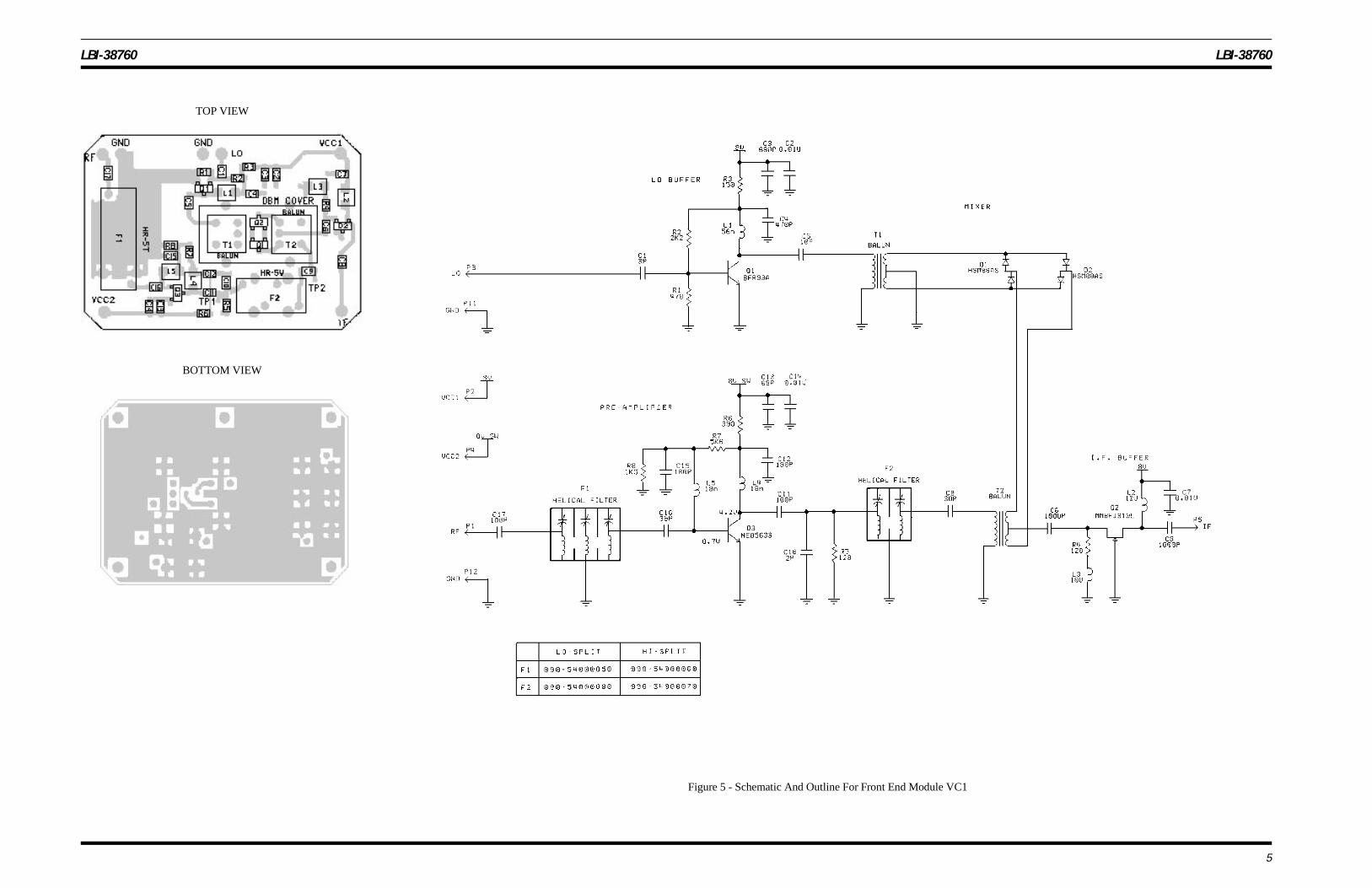
Figure 5 - Schematic And Outline For Front End Module VC1
TOP VIEW
BOTTOM VIEW
LBI-38760 LBI-38760
5

Figure 6 - RX and TX Block Diagram
LBI-38760 LBI-38760
6
Front End Module VC1
RF is coupled from the PA board through a coaxial cable tothe receiver front end. Inside the front end module a pair ofhelical bandpass filters F1 and F2 establish the receiver passband of 12 MHz. The receiver is pretuned at the factory to themost commonly used section of the spectrum, but it may beadjusted to anywhere within the split by tuning the slugs of thefilters.
Q3 is a low noise bipolar amplifier which serves to increasethe sensitivity of the receiver. The first mixer is a double-bal-anced diode type formed by T1, T2, D1 and D2. The first mixerprovides local oscillator-RF isolation along with good inter-modulation and spurious performance. The mixer assembly isshielded to prevent stray magnetic fields from affecting thesurrounding circuits. With the gate grounded, JFET Q2 buffersthe IF signal and provides a broadband termination to the mixerIF port ensuring good spurious as well as intermodulationperformance. The local oscillator signal from the synthesizeris amplified by Q1 to a level of + 8 dBm to drive the mixer.
45 MHz IF Module VC2
A first IF frequency of 45 MHz is employed. This modulecontains a band pass crystal filter centered at the first IFfrequency with a bandwidth of 15 kHz to provide part of theselectivity. The IF signal is further amplified and converted tothe second IF frequency of 455 kHz where it is band passfiltered, limited and then de modulated. The IF module oper-ates from a single 5 volt supply.
Receive Switch
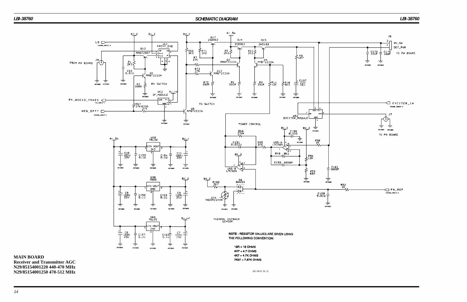
During receive when NEG_DPTT goes high, Q1 and Q13are turned on suppling 8 Volts to Vcc2 of the front end module.The 8 Volts applied to Vcc2 turns on the RF amplifier inside.The reverse happens during transmit.
TRANSMITTER CIRCUIT
The transmitter consists of a fixed tuned 1.5 Watt ExciterModule, a power control circuit and a transmit switch.
Exciter Module U52
The synthesizer drives the exciter module at 0 dBm. ExciterModule U52 operates from a switched 8 volt supply. Themodule is designed for wideband operation and requires noadjustment. Both input and output ports operate at a 50 ohmimpedance level. Output power is varied by means of the AGCvoltage which may be varied between 6 to 12.5 volts.
Power Control Circuit
The function of the power control circuit is to maintain aconstant output power across the band. Thermistor U14 sensesthe temperature inside the radio and reduces the output powerwhen the temperature exceeds a set threshold. This circuitcontrols the supply voltage to the last amplifier in the excitermodule U52.
The DC voltage proportional to the RF output power fromthe detector circuit on the power amplifier board feeds the (+)input of op-amp U55-A. A fixed reference voltage developedby potential divider R54 and R55 feeds the (-) input of the sameamplifier. The difference is amplified and drives the (-) inputof U55-B. The difference between the two inputs is amplifiedand varies the drive to transistor Q4 and Q15. WithNEG_DPTT pulled low by the microprocessor during trans-mit, Q3 and Q14 are turned on. This enables Q15 to vary thesupply voltage to the last amplifier in the exciter module, thusachieving variable output power.
Thermistor U14 and resistor R166 form a variable voltagedivider with temperature. Above a set threshold, diode D8conducts and PA_REF is reduced which then throttles theoutput power down.
Transmit Switch
During transmit, the Microprocessor pulls the NEG_DPTTline low, the collector of Q5 then goes high and turns on Q12.Q12 then supplies the base drive to turn on transistor Q17which provides 8V_SW to the exciter module and the PINdiode switch on the PA Board.
POWER DISTRIBUTION
The audio circuit receives 13 volts from the A + _SW lineon the Main Board. This voltage feeds Regulator U22 andaudio PA U79. The regulator supplies 5 volts to all op-ampsexcept U70. A regulated 1.8 volt bias supply is provided byRegulator U83, operating from the A + _SW line. A regulated8 volt supply is provided by D11 to U70, operating also fromthe A+ _SW line.
Voltage Regulator U63 supplies a regulated 5 volts DC tothe Microprocessor, the EPROM and the latch circuit. A resetcircuit is built into U63 to provide the Microprocessor with areset signal required during its power-up routine.
Transistor circuit Q24 is a filter for the IGN_A + batteryvoltage. This circuit is used to reduce "alternator whine" inter-ference. The filtered A + _FILTER (13 volts) is used in thehandset and on the audio circuit.
The RF circuit is powered by three Regulators U58 U30and U60, which operate from the switched 13.8 volts (A +_SW) line. Regulator U58 supplies 8 volts exclusively forthe VCO to ensure low synthesizer noise. Regulator U30supplies 8 volts to the PLL IC U54, injection amplifier chainQ6, Q22 and Q459 of the synthesizer, U55 in the powercontrol circuit of the transmitter, the Exciter Module U52and also the receiver Front End Module VC 1.
A 5 volt Regulator U60 supplies power to the receiver IFmodule, VCTCXO in the synthesizer and also to the pres-caler.
SERVICE NOTES
AUDIO CIRCUIT
1. Refer to the block diagrams Figures 1 and 2, forproper signal levels and gains for the various audiopaths.
2. All bias point (VB) shown on the audio circuit sche-matic diagram are generated by Regulator U83. Noneof the operational amplifier circuits will operateproperly without this voltage.
When measuring signal levels, remember that theinverting (-) input ports are "virtual grounds." Little
or no measurable AC voltages will be present at theseports.
LOGIC CIRCUIT
DC Checks
Power for the logic circuit is supplied by the 13 volts onJ4-pin 4.
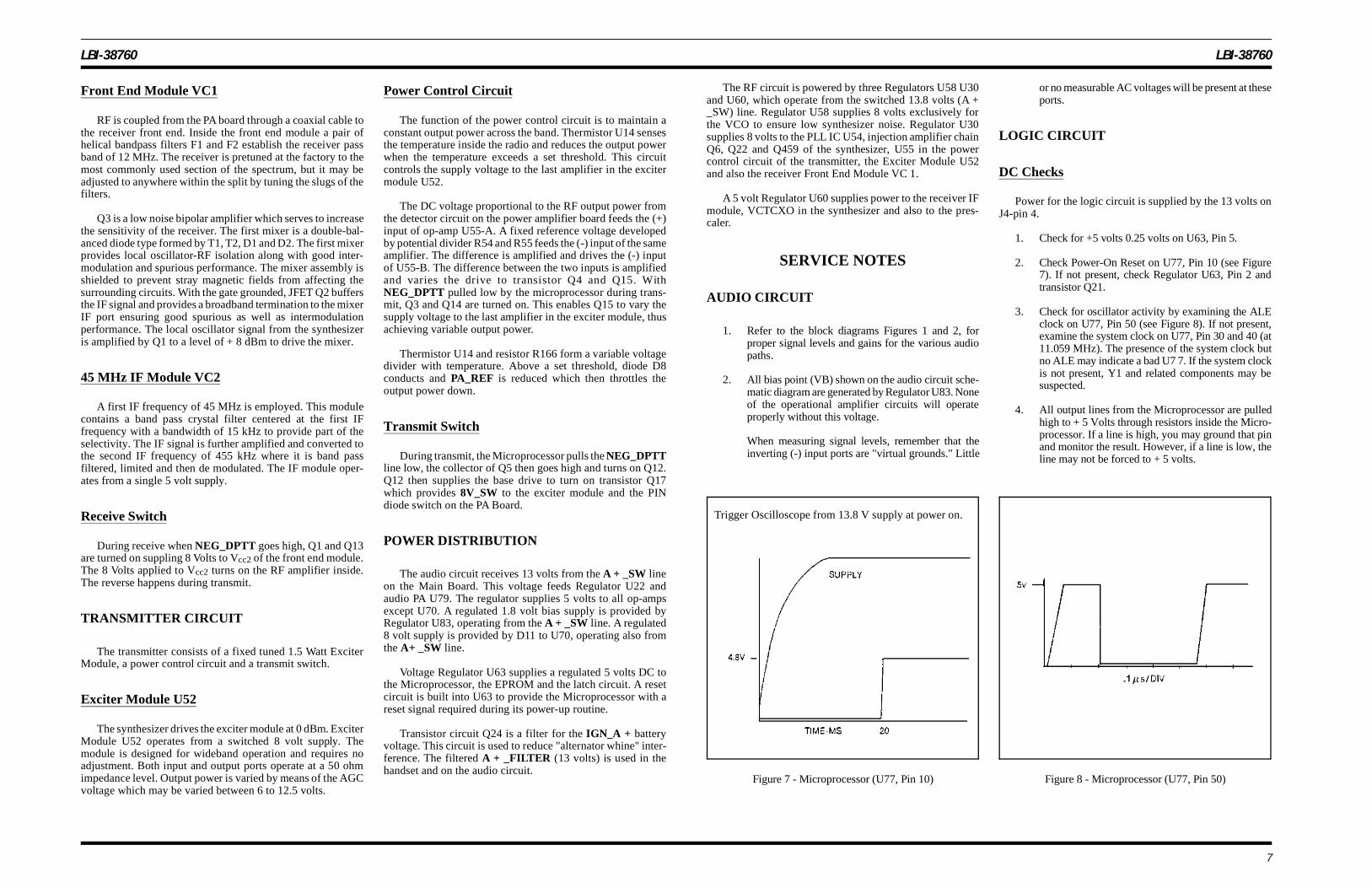
1. Check for +5 volts 0.25 volts on U63, Pin 5.
2. Check Power-On Reset on U77, Pin 10 (see Figure7). If not present, check Regulator U63, Pin 2 andtransistor Q21.
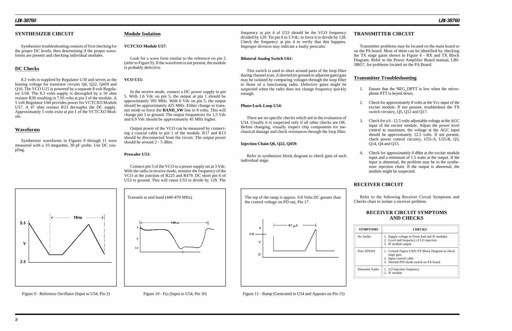
3. Check for oscillator activity by examining the ALEclock on U77, Pin 50 (see Figure 8). If not present,examine the system clock on U77, Pin 30 and 40 (at11.059 MHz). The presence of the system clock butno ALE may indicate a bad U7 7. If the system clockis not present, Y1 and related components may besuspected.
4. All output lines from the Microprocessor are pulledhigh to + 5 Volts through resistors inside the Micro-processor. If a line is high, you may ground that pinand monitor the result. However, if a line is low, theline may not be forced to + 5 volts.
Trigger Oscilloscope from 13.8 V supply at power on.
Figure 7 - Microprocessor (U77, Pin 10) Figure 8 - Microprocessor (U77, Pin 50)
LBI-38760 LBI-38760
7
SYNTHESIZER CIRCUIT
Synthesizer troubleshooting consists of first checking forthe proper DC levels, then determining if the proper wave-forms are present and checking individual modules.
DC Checks
8.2 volts is supplied by Regulator U30 and serves as thebiasing voltage for transistor circuits Q6, Q22, Q459 andQ16. The VCO U15 is powered by a separate 8 volt Regula-tor U58. The 8.2 volts supply is decoupled by a 10 ohmresistor R30 resulting in 7.95 volts at pin 2 of the module. A5 volt Regulator U60 provides power for VCTCXO ModuleU57. A 47 ohm resistor R23 decouples the DC supply.Approximately 5 volts exist at pin 1 of the VCTCXO Mod-ule.
Waveforms
Synthesizer waveforms in Figures 9 through 11 weremeasured with a 10 megaohm, 30 pF probe. Use DC cou-pling.
Module Isolation
VCTCXO Module U57:
Look for a wave form similar to the reference on pin 2(refer to Figure 9). If the waveform is not present, the moduleis probably defective.
VCO U15:
In the receive mode, connect a DC power supply to pin5. With 1.6 Vdc on pin 5, the output at pin 1 should beapproximately 395 MHz. With 6 Vdc on pin 5, the outputshould be approximately 425 MHz. Either change to trans-mit mode or force the BAND_SW line to 8 volts. This willchange pin 3 to ground. The output frequencies for 1,5 Vdcand 6.9 Vdc should be approximately 45 MHz higher.
Output power of the VCO can be measured by connect-ing a coaxial cable to pin 1 of the module. R17 and R13should be disconnected from the circuit. The output powershould be around 2 - 5 dBm.
Prescaler U53:
Connect pin 5 of the VCO to a power supply set at 3 Vdc.With the radio in receive mode, monitor the frequency of theVCO at the junction of R225 and R479. DC short pin 6 ofU53 to ground. This will cause U53 to divide by 129. The
frequency at pin 4 of U53 should be the VCO frequencydivided by 129. Tie pin 6 to 5 Vdc, to force it to divide by 128.Check the frequency at pin 4 to verify that this happens.Improper division may indicate a faulty prescaler.
Bilateral Analog Switch U61:
This switch is used to short around parts of the loop filterduring channel scan. A shorted (to ground or adjacent gate) gatemay be isolated by comparing voltages through the loop filterto those of a functioning radio. Defective gates might besuspected when the radio does not change frequency quicklyenough.
Phase-Lock-Loop U54:
There are no specific checks which aid in the evaluation ofU54. Usually it is suspected only if all other checks are OK.Before changing, visually inspect chip components for me-chanical damage and check resistances through the loop filter.
Inject ion Chain Q6, Q22, Q459:
Refer to synthesizer block diagram to check gain of eachindividual stage.
TRANSMITTER CIRCUIT
Transmitter problems may be located on the main board oron the PA board. Most of them can be identified by checkingthe TX stage gains shown in Figure 6 - RX and TX BlockDiagram. Refer to the Power Amplifier Board manual, LBI-38657, for problems located on the PA Board.
Transmitter Troubleshooting
1. Ensure that the NEG_DPTT is low when the micro-phone PTT is keyed down.
2. Check for approximately 8 volts at the Vcc input of theexciter module. If not present, troubleshoot the TXswitch circuitry, Q5, Q12 and Q17.
3. Check for a 6 - 12.5 volts adjustable voltage at the AGCinput of the exciter module. Adjust the power levelcontrol to maximum, the voltage at the AGC inputshould be approximately 12.5 volts. If not present,check power control circuitry, U55-A, U55-B, Q3,Q14, Q4 and Q15.
4. Check for approximately 0 dBm at the exciter moduleinput and a minimum of 1.5 watts at the output. If theinput is abnormal, the problem may be in the synthe-sizer injection chain. If the output is abnormal, themodule might be suspected.
RECEIVER CIRCUIT
Refer to the following Receiver Circuit Symptoms andChecks chart to isolate a receiver problem.
RECEIVER CIRCUIT SYMPTOMSAND CHECKS
SYMPTOMS CHECKS
No Audio 1. Supply voltage to Front End and IF modules2. Level and frequency of LO injection3. IF module output
Poor SINAD 1. Consult Figure 6 RX-TX Block Diagram to check stage gain2. Input coaxial cable3. Shorted PIN diode switch on PA board
Distorted Audio 1. LO injection frequency2. IF module
Figure 9 - Reference Oscillator (Input to U54, Pin 2)
Transmit at mid band (440-470 MHz)
Figure 10 - FIN (Input to U54, Pin 10)
The top of the ramp is approx. 0.8 Volts DC greater thanthe control voltage on PD out, Pin 17.
Figure 11 - Ramp (Generated in U54 and Appears on Pin 15)
LBI-38760 LBI-38760
8
MAIN BOARDN29/85154001220 440-470 MHzN29/85154001250 470-512 MHz
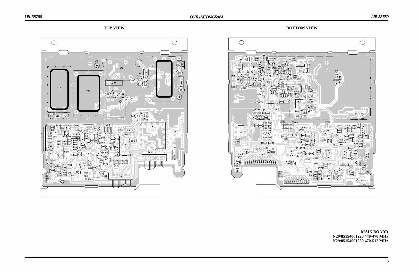
OUTLINE DIAGRAM
TOP VIEW BOTTOM VIEW
LBI-38760 LBI-38760
9

SCHEMATIC DIAGRAM
MAIN BOARDCPUN29/85154001220 440-470 MHzN29/85154001250 470-512 MHz (RC-8670, Sh. 1)
LBI-38760 LBI-38760
10
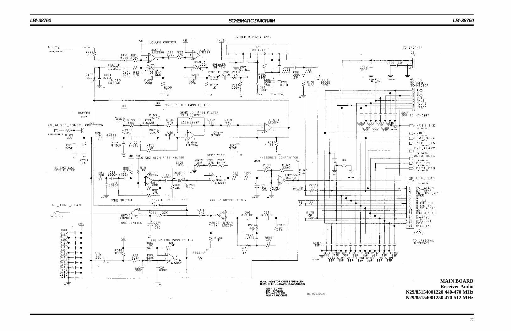
SCHEMATIC DIAGRAM
MAIN BOARDReceiver Audio
N29/85154001220 440-470 MHzN29/85154001250 470-512 MHz
(RC-8670, Sh. 2)
LBI-38760 LBI-38760
11
SCHEMATIC DIAGRAM
MAIN BOARDTransmitter AudioN29/85154001220 440-470 MHzN29/85154001250 470-512MHHz (RC-8670, Sh. 3)
LBI-38760 LBI-38760
12
SCHEMATIC DIAGRAM
MAIN BOARDSynthesizer
N29/85154001220 440-470 MHzN29/85154001250 470-512 MHz(RC-8670, Sh. 4)
LBI-38760 LBI-38760
13
SCHEMATIC DIAGRAM
MAIN BOARDReceiver and Transmitter AGCN29/85154001220 440-470 MHzN29/85154001250 470-512 MHz (RC-8670, Sh. 5)
LBI-38760 LBI-38760
14
IC DATA
U1 - EPROM (27C256)
U3 - LATCH (74HC373)
DSW1 & DSW2 - DIGITAL TRIMPOT
LBI-38760 LBI-38760
15

IC DATA
U7, U10, U16, U55, U64, U65, U70& U75 - OPERATIONAL AMPLIFIER(LM2904)
U22 & U30 - POSITIVE VOLTAGEREGLATOR (NJM7800A)
U53 - TWO MODULAS PRESCALER (MB501/MB501L)
U54 - PHASE LOCK LOOP (MC145159)
U58 & U60 - VOLTAGE REGULATOR U61 - QUAD ANALOG SWITCH (MC14066B)
U63 - REGULATOR WITH RESET (L387A)
LBI-38760 LBI-38760
16
IC DATA
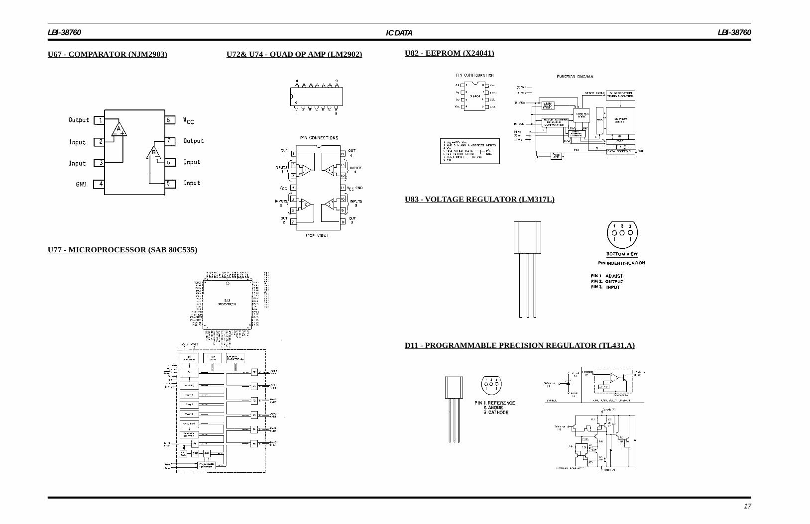
U67 - COMPARATOR (NJM2903)
U77 - MICROPROCESSOR (SAB 80C535)
U72& U74 - QUAD OP AMP (LM2902) U82 - EEPROM (X24041)
U83 - VOLTAGE REGULATOR (LM317L)
D11 - PROGRAMMABLE PRECISION REGULATOR (TL431,A)
LBI-38760 LBI-38760
17
IC DATA
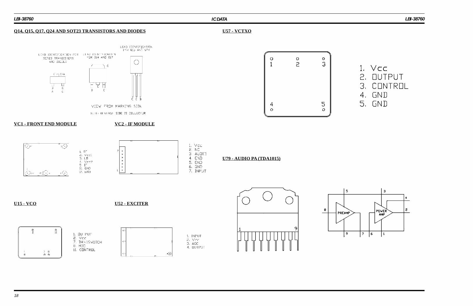
Q14, Q15, Q17, Q24 AND SOT23 TRANSISTORS AND DIODES
VC1 - FRONT END MODULE VC2 - IF MODULE
U15 - VCO U52 - EXCITER
U57 - VCTXO
U79 - AUDIO PA (TDA1015)
LBI-38760 LBI-38760
18

MDS CONVENTIONAL RADIO (UHF)MAIN BOARD ASSEMBLY
N29/85154001220 440-470 MHzN29/85154001250 470-512 MHz
ISSUE 2
MAIN BOARD
PARTS LIST
SYMBOL PART NUMBER DESCRIPTION
— — — — CAPACITOR — — —
C13 19A701225P2 Electrolytic: 10 µF, 25 V.
C16 19A702052P33 Surface Mount: 0.1 µF, 25 V.
C17 Surface Mount: 2700 pF, 50 V.
C20 19A702052P5 Surface Mount: 1000 pF, 50 V.
C21 Electrolytic: 1000 µF, 50 V.
C22 19A702052P5 Surface Mount: 1000 µF, 50 V.thruC24
C26 19A702052P5 Surface Mount: 1000 µF, 50 V.andC27
C28 19A702052P33 Surface Mount: 0.1 µF, 25 V.
C29 19A702061P61 Surface Mount: 100 pF, 50 V.
C31 19A702061P61 Surface Mount: 100 pF, 50 V.
C32 19A702061P77 Surface Mount: 470 pF, 50 V.
C34 19A702052P28 Surface Mount: .022 µF, 50 V.
C35 19A149896P118 Surface Mount: .0056 µF, 50 V.
C37 19A701371P7 Polyester: .01 µF, 100 V.
C38 19A702052P14 Surface Mount: .01 µF, 50 V.
C39 19A702052P28 Surface Mount: .022 µF, 50 V.
C40 19A701371P7 Polyester: .01 µF, 100 V.
C42 19A702052P33 Surface Mount: 0.1 µF, 25 V.
C43 Electrolytic: 1000 µF, 50 V.
C45 Surface Mount: 820 pF, 50 V.
C48 19A702052P110 Surface Mount: .0047 µF, 50 V.
C49 19A702052P112 Surface Mount: .0068 µF, 50 V.
C50 19A702052P33 Surface Mount: 0.1 µF, 25 V.
C51 19A702236P44 Surface Mount: 56 pF, 50 V.
C52 19A702052P33 Surface Mount: 0.1 µF, 25 V.
C57 19A702052P33 Surface Mount: 0.1 µF, 25 V.
C59 19A702052P20 Surface Mount: .033 µF, 50 V.
C60 19A702061P77 Surface Mount: 470 pF, 50 V.thruC62
C63 19A702052P33 Surface Mount: 0.1 µF, 25 V.
C64 19A702061P77 Surface Mount: 470 pF, 50 V.andC65
C66 19A702052P33 Surface Mount: 0.1 µF, 25 V.thruC71
C73 19A702236P38 Surface Mount: 33 pF, 50 V.
* COMPONENTS, ADDED, DELETED OR CHANGED BY PRODUCTION CHANGES
SYMBOL PART NUMBER DESCRIPTION
C74 19A702052P33 Surface Mount: 0.1 µF, 25 V.thruC78
C79 Surface Mount: 510 pF, 50 V.
C80 19A702052P33 Surface Mount: 0.1 µF, 25 V.
C84 Surface Mount: 510 pF, 50 V.
C85 19A703314P12 Electrolytic: 100 µF, 25 V.andC86
C87 Electrolytic: 1000 µF, 25 V.
C88 19A702052P33 Surface Mount: 0.1 µF, 25 V.
C89 19A701225P9 Electrolytic: 220 µF, 25 V.
C90 19A701534P9 Tantalum: 47 µF, 6.3 V.
C92 19A702052P20 Surface Mount: .033 µF, 50 V.
C93 19A702052P33 Surface Mount: 0.1 µF, 25 V.thruC102
C105 19A702061P61 Surface Mount: 100 pF, 50 V.
C106 19A702052P33 Surface Mount: 0.1 µF, 25 V.
C108 19A701225P9 Electrolytic: 220 µF, 25 V.
C109 19A702061P61 Surface Mount: 100 pF, 50 V.
C110 19A702061P77 Surface Mount: 470 pF, 50 V.thruC115
C119 19A702052P112 Surface Mount: .0068 µF, 50 V.
C121 19A702052P33 Surface Mount: 0.1 µF, 25 V.
C122 19A702061P77 Surface Mount: 470 pF, 50 V.
C124 19A702061P61 Surface Mount: 100 pF, 50 V.thruC126
C127 19A703314P12 Electrolytic: 100 µF, 25 V.
C129 19A702236P38 Surface Mount: 33 pF, 50 V.thruC131
C132 19A702052P5 Surface Mount: 1000 pF, 50 V.
C180 19A702236P42 Surface Mount: 47 pF, 50 V.
C181 19A702052P33 Surface Mount: 0.1 µF, 25 V.
C184 19A702236P38 Surface Mount: 33 pF, 50 V.
C186 19A702236P38 Surface Mount: 33 pF, 50 V.andC196
C197 19A702236P38 Surface Mount: 33 pF, 50 V.thruC202
C204 19A701225P2 Electrolytic: 10 µF, 25 V.
C207 19A702236P38 Surface Mount: 33 pF, 50 V.andC227
C230 19A702052P5 Surface Mount: 1000 pF, 50 V.
C231 19A702052P33 Surface Mount: 0.1 µF, 25 V.
C248 19A702052P28 Surface Mount: .022 µF, 50 V.
C252 19A702052P110 Surface Mount: .0047 µF, 50 V.
C253 Surface Mount: .22 µF, 16 V.
C260 19A702236P38 Surface Mount: 33 pF, 50 V.
SYMBOL PART NUMBER DESCRIPTION
C265 19A702236P38 Surface Mount: 33 pF, 50 V.andC266
C461 19A701225P2 Electrolytic: 10 µF, 25 V.
C462 19A702052P14 Surface Mount: .01 µF, 50 V.
C471 19A702052P33 Surface Mount: 0.1 µF, 25 V.
C498 19A702052P33 Surface Mount: 0.1 µF, 25 V.
C499 19A702236P38 Surface Mount: 33 pF, 50 V.
C507 19A149896P112 Surface Mount: 1800 pF, 50 V.
C508 19A703314P7 Electrolytic: 2.2 µF, 35 V.
C900 19A702052P33 Surface Mount: 0.1 µF, 25 V.
C901 19A703314P5 Electrolytic: 22 µF, 25 V.
C903 19A702061P77 Surface Mount: 470 pF, 50 V.
— — — — — DIODE — — — —
D2 19700053P1 Diode: BAV99.thruD6
D7 T324ADP1032 Rectifier: 1N4003.
D9 19A700053P1 Diode: BAV99.
D11 19A702939P2 Programmable Precision Regualtor: TL461CLP.
D21 BAS16 Diode: 75V 0.25A BAS-16.
D22 ECG4926 Zener: 18V, 1N6277A.
— — — — TRIMPOTS — — — —
DSW1 Surface Mount: Digital Trimpot.andDSW2
— — — — — JACKS — — — —
J5 N29/14954000020 Modular mic jack, 8-way.
— — — — RESISTORS — — —
R3 Surface Mount: 0 ohms, 1/10 w.
R53 19B801251P472 Surface Mount: 4.7K ohms, 1/10 w.
R18 19B801251P103 Surface Mount: 10K ohms, 1/10 w.
R51 19B801251P103 Surface Mount: 10K ohms, 1/10 w.
R74 19B801251P561 Surface Mount: 560 ohms, 1/10 w.
R80 19B801251P824 Surface Mount: 820K ohms, 1/10 w.
R81 19B801251P274 Surface Mount: 270K ohms, 1/10 w.
R82 19B801251P273 Surface Mount: 27K ohms, 1/10 w.
R83 19B801251P153 Surface Mount: 15K ohms, 1/10 w.
R84 19B801251P333 Surface Mount: 33K ohms, 1/10 w.
R85 19B801251P824 Surface Mount: 820K ohms, 1/10 w.
R86 19B801251P103 Surface Mount: 10K ohms, 1/10 w.
R87 19B801251P473 Surface Mount: 47K ohms, 1/10 w.
R88 19B801251P683 Surface Mount: 68K ohms, 1/10 w.
R90 19B801251P273 Surface Mount: 27K ohms, 1/10 w.
R91 19B801251P153 Surface Mount: 15K ohms, 1/10 w.
R92 19B801251P273 Surface Mount: 27K ohms, 1/10 w.
R93 19B801251P224 Surface Mount: 220K ohms, 1/10 w.
SYMBOL PART NUMBER DESCRIPTION
R95 19B801251P333 Surface Mount: 33K ohms, 1/10 w.
R98 19B801251P273 Surface Mount: 27K ohms, 1/10 w.
R106 19B801251P102 Surface Mount: 1.0K ohms, 1/10 w.
R109 19B801251P102 Surface Mount: 1.0K ohms, 1/10 w.
R111 19B801251P104 Surface Mount: 100K ohms, 1/10 w.
R112 19B801251P102 Surface Mount: 1.0K ohms, 1/10 w.
R113 19B801251P562 Surface Mount: 5.6K ohms, 1/10 w.
R116 19B801251P103 Surface Mount: 10K ohms, 1/10 w.
R118 19B801251P102 Surface Mount: 1.0K ohms, 1/10 w.
R119 19B801251P473 Surface Mount: 47K ohms, 1/10 w.
R122 19B801251P332 Surface Mount: 3.3K ohms, 1/10 w.andR123
R127 19B801251P102 Surface Mount: 1.0K ohms, 1/10 w.andR128
R131 19B801251P823 Surface Mount: 82K ohms, 1/10 w.
R132 19B801251P153 Surface Mount: 15K ohms, 1/10 w.
R133 19B801251P182 Surface Mount: 1.8K ohms, 1/10 w.andR134
R135 19B801251P273 Surface Mount: 27K ohms, 1/10 w.
R138 19B801251P471 Surface Mount: 470 ohms, 1/10 w.
R139 19B801251P104 Surface Mount: 100K ohms, 1/10 w.
R140 19B801251P334 Surface Mount: 330K ohms, 1/10 w.
R141 19B801251P222 Surface Mount: 2.2K ohms, 1/10 w.
R142 19B801251P224 Surface Mount: 220K ohms, 1/10 w.
R143 19B801251P472 Surface Mount: 4.7K ohms, 1/10 w.
R147 19B801251P102 Surface Mount: 1.0K ohms, 1/10 w.
R148 19B801251P123 Surface Mount: 12K ohms, 1/10 w.
R151 Surface Mount: 4.7 ohms, 1/10 w.
R153 19B801251P563 Surface Mount: 56K ohms, 1/10 w.
R154 19B801251P102 Surface Mount: 1.0K ohms, 1/10 w.
R155 19B801251P563 Surface Mount: 56K ohms, 1/10 w.
R156 19B801251P102 Surface Mount: 1.0K ohms, 1/10 w.
R157 19B801251P103 Surface Mount: 10K ohms, 1/10 w.
R158 19B801251P220 Surface Mount: 22 ohms, 1/10 w.
R159 19B801251P102 Surface Mount: 1.0K ohms, 1/10 w.
R160 19B801251P392 Surface Mount: 3.9K ohms, 1/10 w.
R161 19B801251P222 Surface Mount: 2.2K ohms, 1/10 w.
R162 19B801251P102 Surface Mount: 1.0K ohms, 1/10 w.
R163 19B801251P154 Surface Mount: 150K ohms, 1/10 w
R164 19B801251P152 Surface Mount: 1.5K ohms, 1/10 w.
R165 19B801251P332 Surface Mount: 3.3K ohms, 1/10 w.
R167 19B801251P681 Surface Mount: 680 ohms, 1/10 w.
R169 19B801251P102 Surface Mount: 10K ohms, 1/10 w.
R170 19B801251P223 Surface Mount: 22K ohms, 1/10 w.
R171 19B801251P153 Surface Mount: 15K ohms, 1/10 w.
R172 Surface Mount: 75K ohms, 1/10 w.
LBI-38760 LBI-38760
19
MAIN BOARD
PARTS LIST
SYMBOL PART NUMBER DESCRIPTION
R173 19B801251P472 Surface Mount: 4.7K ohms, 1/10 w.
R174 19B801251P104 Surface Mount: 100K ohms, 1/10 w.
R175 Surface Mount: 0 ohms, 1/10 w.
R176 19B801251P103 Surface Mount: 10K ohms, 1/10 w.
R177 19B801251P223 Surface Mount: 22K ohms, 1/10 w.
R178 19B801251P104 Surface Mount: 100K ohms, 1/10 w.
R179 19B801251P332 Surface Mount: 3.3K ohms, 1/10 w.
R180 19B801251P153 Surface Mount: 15K ohms, 1/10 w.
R181 19B801251P334 Surface Mount: 330K ohms, 1/10 w.
R182 19B801251P153 Surface Mount: 15K ohms, 1/10 w.
R183 19B801251P124 Surface Mount: 120K ohms, 1/10 w.
R184 19B801251P272 Surface Mount: 2.7K ohms, 1/10 w.
R185 19B801251P153 Surface Mount: 15K ohms, 1/10 w.
R186 Surface Mount: 49.9K ohms, 1/10 w.
R187 19B801251P104 Surface Mount: 100K ohms, 1/10 w.
R188 Surface Mount: 200K ohms, 1/10 w.
R189 Surface Mount: 402K ohms, 1/10 w.
R190 Surface Mount: 806K ohms, 1/10 w.
R191 19B801251P124 Surface Mount: 120 ohms, 1/10 w.
R192 19B801251P271 Surface Mount: 270 ohms, 1/10 w.
R193 19B801251P472 Surface Mount: 4.7K ohms, 1/10 w.
R194 19B801251P222 Surface Mount: 2.2K ohms, 1/10 w.
R195 19B801251P472 Surface Mount: 4.7K ohms, 1/10 w.
R196 19B801251P333 Surface Mount: 33K ohms, 1/10 w.
R198 19B801251P393 Surface Mount: 39K ohms, 1/10 w.
R199 19B801251P102 Surface Mount: 1.0K ohms, 1/10 w.thruR204
R208 19B801251P563 Surface Mount: 56K ohms, 1/10 w.andR209
R210 19B801251P103 Surface Mount: 10K ohms, 1/10 w.
R211 19B801251P152 Surface Mount: 1.5K ohms, 1/10 w.
R213 19B801251P102 Surface Mount: 1.0K ohms, 1/10 w.thruR215
R217 19B801251P102 Surface Mount: 1.0K ohms, 1/10 w.thruR218
R219 19B801251P153 Surface Mount: 15K ohms, 1/10 w.
R230 19B801251P102 Surface Mount: 1.0K ohms, 1/10 w.
R231 19B801251P223 Surface Mount: 22K ohms, 1/10 w.
R232 19B801251P220 Surface Mount: 22 ohms, 1/8 w.
R233 Surface Mount: 0 ohms, 1/10 w.
R317 Surface Mount: 0 ohms, 1/10 w.
R331 19B801251P273 Surface Mount: 27K ohms, 1/10 w.
R459 19B801251P332 Surface Mount: 3.3K ohms, 1/10 w.
R468 19B801251P222 Surface Mount: 2.2K ohms, 1/10 w.
R471 19B801251P223 Surface Mount: 22K ohms, 1/10 w.
R472 Surface Mount: 0 ohms, 1/10 w.
R473 19B801251P182 Surface Mount: 1.8K ohms, 1/10 w.
R501 19B801251P103 Surface Mount: 10K ohms, 1/10 w.
SYMBOL PART NUMBER DESCRIPTION
R502 19B801251P473 Surface Mount: 47K ohms, 1/10 w.andR503
R506 19B801251P104 Surface Mount: 100K ohms, 1/10 w.
R514 19B801251P223 Surface Mount: 22K ohms, 1/10 w.
R517 19B801251P682 Surface Mount: 6.8K ohms, 1/10 w.
R900 Surface Mount: 0 ohms, 1/10 w.
R901 19B801251P102 Thermistor: 1K ohms, 1/10 w.
R902 Surface Mount: 0 ohms, 1/10 w.
R904 Surface Mount: 0 ohms, 1/10 w.andR905
R906 19B801251P273 Surface Mount: 27K ohms, 1/10 w.
R907 19B801251P332 Surface Mount: 3.3K ohms, 1/10 w.
— — — INTEGRATED CIRCUIT — —
U1 344A3732G1 EPROM (Programmed IC, contains software).
U2 Capacitor: 22 pF, 100 V DSS310.
U3 344A3064P202 Surface Mount: LATCH MC74HC373.
U7 LM2904D OP AMP, Dual: NJM2904M.
U10 LM2904D OP AMP, Dual: NJM2904M.
U16 LM2904D OP AMP, Dual: NJM2904M.
U22 19A134717P1 REGULATOR: NJM7805A.
U63 19A704970P1 REGULATOR: L387A.
U64 LM2904D OP AMP, Dual: LM2904D.
U65 LM2904D OP AMP, Dual: NJM2904M.
U67 19A704125P3 COMPARATOR: NJM2903M.
U70 LM2904D OP AMP, Dual: NJM2904M.
U72 LM2902D OP AMP, Quad: LM2902D.
U74 LM2902D OP AMP, Quad: LM2902D.
U75 LM2904D OP AMP, Dual: NJM2904M.
U76 N29/26300000150 RELAY: LM44D00.
U77 N29/22154000060 MICROPROCESSOR, CMOS: SABBOC535-T40/85.
U79 TDA1015 Integrated Circuit: TDA1015.
U82 Integrated Circuit, CMOS: X24C04I 8DIL.
U83 J19/130-0236 REGULATOR: LM317LBZ .
— — — — TRANSISTORS — — —
Q11 19A700076P2 Transistor, NPN: 200 mA 40V, MMBT3904.
Q19 BT2222A Transistor, NPN: 600 mA 40V, PMBT2222A.
Q20 BT2907 Transistor, PNP: MMBT2907.andQ21
Q23 BT2222A Transistor, NPN: 600 mA 40V, PMBT2222A.
Q24 ECG 184 Transistor, NPN: 2N5190.
Q165 ECG 184 Transistor, NPN: 2N5190.
— — — — — CABLES — — — — —
W4 N29/85154001691 Cable assembly, 4-wire (PA board to Main Board).
SYMBOL PART NUMBER DESCRIPTION
W7 N29/85101700920 Flat ribbon cable, 16-wire.
— — — — CRYSTALS — — — —
Y1 N29/08054000190 Crystal: 11.0592 MHz.
— — — MISCELLANEOUS— — —
N29/40354000252 Cover, top or bottom.
N29/40354000232 Mounting bracket.
N29/40354000870 Ring terminal.
N29/85154001652 Power cable assembly, with fuses (completely external to the radio).
N29/39120403052 Screw: M2.6 x 12. (Quantity of 4).
N29/39154005012 Screw, hex, Philips: M4 x 8. (Used to secure mounting bracket, Quantity of 2).
N29/39254000032 Washer, plain: M4. (Used to secure mounting bracket, Quantity of 2).
Screw: M2.6 x 8. (Used to mount top and bottom covers, Quantity of 4).
Washer, plain: M2.6. (Used to mount top and bottom covers, Quantity of 4).
Washer, spring: M2.6. (Used to mount top and bottom covers, Quantity of 4).
Nut: M2.6. (Quantity of 1).
Screw, Taptite: M2 x 6. (Quantity of 16).
Screw: M4 x 30. (Used to secure heatsink, Quantity of 2).
Clip, shielding.
Clip, regulator. (Quantity of 2).
Shield.
Clip.
Shield-Cavity.
Shield-Core.
Shielding pad.
Clip-Q15.
IC socket, 28 pin.
SYNTHESIZER
— — — — CAPACITORS — — —
C1 19A703314P4 Electrolytic: 47 µF, 16 V.andC2
C3 19A701225P9 Electrolytic: 220 µF, 25 V.andC4
C5 19A703314P4 Electrolytic: 47 µF, 16 V.
C12 19A701225P9 Electrolytic: 220 µF, 25 V.
C82 19A702052P14 Surface Mount: .01 µF, 50 V.
C103 19A702052P14 Surface Mount: .01 µF, 50 V.
C104 19A702052P5 Surface Mount: 1000 pF, 50 V.
C117 19A700061P61 Surface Mount: 100 pF, 50 V.
C118 19A702052P14 Surface Mount: .01 µF, 50 V.
SYMBOL PART NUMBER DESCRIPTION
C120 19A702052P14 Surface Mount: .01 µF, 50 V.
C133 19A702052P5 Surface Mount: 1000 pF, 50 V.
C134 Surface Mount: 110 pF, 50 V.
C135 19A702052P5 Surface Mount: 1000 pF, 50 V.
C136 19A702236P10 Surface Mount: 2.0 pF, 50 V.
C137 19A702061P61 Surface Mount: 100 pF, 50 V.
C138 Capacitor: .022 µF, 100 V.
C139 Capacitor: 0.1 µF, 400 V.
C140 19A702052P5 Surface Mount: 1000 pF, 50 V.andC141
C143 19A702052P5 Surface Mount: 1000 pF, 50 V.
C145 19A702052P14 Surface Mount: .01 µF, 50 V.
C146 19A702052P5 Surface Mount: 1000 pF, 50 V.
C147 Surface Mount: 110 pF, 50 V.
C148 19A702052P5 Surface Mount: 1000 pF, 50 V.
C149 19A702061P61 Surface Mount: 100 pF, 50 V.
C150 19A702052P5 Surface Mount: 1000 pF, 50 V.
C152 19A702061P61 Surface Mount: 100 pF, 50 V.
C154 19A702061P61 Surface Mount: 100 pF, 50 V.
C156 19A702052P14 Surface Mount: .01 µF, 50 V.
C167 Surface Mount: 510 pF, 50 V.
C168 19A702236P38 Surface Mount: 33 pF, 50 V.
C169 19A702052P5 Surface Mount: 1000 pF, 50 V.
C170 19A702236P10 Surface Mount: 2.0 pF, 50 V.
C171 Surface Mount: 110 pF, 50 V.
C172 19A702052P14 Surface Mount: .01 µF, 50 V.
C173 19A702061P61 Surface Mount: 100 pF, 50 V.
C174 19A702052P14 Surface Mount: .01 µF, 50 V.
C175 19A702061P61 Surface Mount: 100 pF, 50 V.
C203 19A702061P61 Surface Mount: 100 pF, 50 V.
C229 19A702236P42 Surface Mount: 47 pF, 50 V.
C313 19A702061P61 Surface Mount: 100 pF, 50 V.
C466 19A702236P10 Surface Mount: 2.0 pF, 50 V.
— — — — TRANSISTORS — — —
Q6 BFR93A NPN: BFR93A.andQ7
Q16 BT2907 PNP: MMBT2907.
Q22 BFR93A NPN: BFR93A.
— — — — RESISTORS — — —
R4 19B801251P331 Surface Mount: 330 ohms, 1/10 w.
R12 19B801251P120 Surface Mount: 12 ohms, 1/10 w.
R13 19B801251P390 Surface Mount: 39 ohms, 1/10 w.
R14 19B801251P121 Surface Mount: 120 ohms, 1/10 w.
R15 19B801251P152 Surface Mount: 1.5K ohms, 1/10 w.
R16 19B801251P221 Surface Mount: 220 ohms, 1/10 w.
LBI-38760 LBI-38760
20
MAIN BOARD
PARTS LIST
SYMBOL PART NUMBER DESCRIPTION
R17 19B801251P121 Surface Mount: 120 ohms, 1/10 w.
R20 19B801251P100 Surface Mount: 10 ohms, 1/10 w.
R22 19B801251P221 Surface Mount: 220 ohms, 1/10 w.
R23 19B801251P470 Surface Mount: 47 ohms, 1/10 w.
R26 19B801251P221 Surface Mount: 220 ohms, 1/10 w.
R27 19B801251P120 Surface Mount: 12 ohms, 1/10 w.
R28 19B801251P221 Surface Mount: 220 ohms, 1/10 w.
R29 19B801251P100 Surface Mount: 10 ohms, 1/10 w.andR30
R31 19B801251P183 Surface Mount: 18K ohms, 1/10 w.
R32 19B801251P122 Surface Mount: 1.2K ohms, 1/10 w.
R33 19B801251P102 Surface Mount: 1.0K ohms, 1/10 w.
R34 19B801251P104 Surface Mount: 100K ohms, 1/10 w.
R35 19B801251P332 Surface Mount: 3.3K ohms, 1/10 w.
R36 19B801251P472 Surface Mount: 4.7K ohms, 1/10 w.
R37 19B801251P471 Surface Mount: 470 ohms, 1/10 w.
R38 19B801251P104 Surface Mount: 100K ohms, 1/10 w.
R39 19B801251P124 Surface Mount: 120K ohms, 1/10 w.
R40 19B801251P824 Surface Mount: 820K ohms, 1/10 w.
R41 19B801251P683 Surface Mount: 68K ohms, 1/10 w.
R42 19B801251P222 Surface Mount: 2.2K ohms, 1/10 w.andR43
R44 19B801251P332 Surface Mount: 3.3K ohms, 1/10 w.
R45 19B801251P472 Surface Mount: 4.7K ohms, 1/10 w.
R46 19B801251P330 Surface Mount: 33 ohms, 1/10 w.
R47 19B801251P221 Surface Mount: 220 ohms, 1/10 w.
R56 19B801251P473 Surface Mount: 47K ohms, 1/10 w.
R57 19B801251P332 Surface Mount: 3.3K ohms, 1/10 w.andR58
R59 19B801251P473 Surface Mount: 47K ohms, 1/10 w.
R60 19B801251P332 Surface Mount: 3.3K ohms, 1/10 w.
R61 19B801251P473 Surface Mount: 47K ohms, 1/10 w.
R63 19B801251P102 Surface Mount: 1.0K ohms, 1/10 w.
R64 19B801251P152 Surface Mount: 1.5K ohms, 1/10 w.
R68 19B801251P222 Surface Mount: 2.2K ohms, 1/10 w.
R70 19B801251P221 Surface Mount: 220 ohms, 1/10 w.
R75 Surface Mount: 0 ohms, 1/10 w.
R76 19B801251P121 Surface Mount: 120 ohms, 1/10 w.
R197 Surface Mount: 0 ohms, 1/10 w.
R205 19B801251P820 Surface Mount: 82 ohms, 1/10 wthruR207
R220 19B801251P121 Surface Mount: 120 ohms, 1/10 w.andR221
R222 19B801251P560 Surface Mount: 56 ohms, 1/10 w.
R223 19B801251P120 Surface Mount: 12 ohms, 1/10 w.
R224 19B801251P100 Surface Mount: 10 ohms, 1/10 w.
SYMBOL PART NUMBER DESCRIPTION
R225 19B801251P180 Surface Mount: 18 ohms, 1/10 w.
R226 19B801251P121 Surface Mount: 120 ohms, 1/10 w.
R227 19B800902P5 Surface Mount: 0 ohms, 1/10 w.
R228 19B801251P221 Surface Mount: 220 ohms, 1/10 w.
R229 19B801251P560 Surface Mount: 56 ohms, 1/10 w.
R360 19B801251P152 Surface Mount: 1.5K ohms, 1/10 w.
R479 19B801251P100 Surface Mount: 10 ohms, 1/10 w.
R480 19B801251P222 Surface Mount: 2.2K ohms, 1/10 w.
R495 19B801251P180 Surface Mount: 18 ohms, 1/10 w.
— — INTEGRATED CIRCUIT — —
U15 N29/SMR11 VCO Module. (440-470 MHz).
U15 N29/SMR10 VCO Module. (470-512 MHz).
U53 N29/22100000123 PRESCALER: MB501PF.
U54 19B800902P5 Integrated Circuit: CMOS MC145159FN1.
U57 N29/31854000040 VCTCXO: 12.8 MHz ASD3004B.
U61 19A702705P1 Integrated Circuit: MC14066BD.
TRANSMITTER
— — — CAPACITORS— — — —
C6 19A703314P12 Electrolytic: 100 µF, 25 V.thruC11
C107 19A701534P8 Polyester: 22 µF, 16 V.
C151 19A702052P28 Surface Mount: .022 µF, 50 V.
C153 19A702052P112 Surface Mount: 6800 pF, 50 V.
C155 19A702052P14 Surface Mount: .01 µF, 50 V.
C157 19A702052P33 Surface Mount: 0.1 µF, 50 V.thruC159
C160 19A702052P14 Surface Mount: .01 µF, 50 V.
C161 19A702052P5 Surface Mount: 1000 pF, 50 V.
C162 19A702052P33 Surface Mount: 0.1 µF, 50 V.thruC164
C178 19A702061P61 Surface Mount: 100 pF, 50 V.andC179
— — — — — DIODE — — — — —
D8 19A700053P1 Surface Mount: BAV99.
— — — TRANSISTORS — — —
Q14 2SB962 Surface Mount, PNP: 3A, 30V, 2SB962-ZQ.
Q15 ECG 185 PNP: 2N5193.
Q17 2SB962 Surface Mount, PNP: 3A, 30V, 2SB962-ZQ.
— — — — RESISTORS — — — —
R5 19B801251P222 Surface Mount: 2.2K ohms, 1/10 w.
R6 19B801251P391 Surface Mount: 390 ohms, 1/10 w.
R7 19B801391P273 Surface Mount: 27K ohms, 1/10 w.
SYMBOL PART NUMBER DESCRIPTION
R8 19B801251P391 Surface Mount: 390 ohms, 1/10 w.
R9 Surface Mount: 4.7 ohms, 1/10 w.
R10 19B801251P822 Surface Mount: 8.2K ohms, 1/10 w.
R11 19B801251P102 Surface Mount: 10K ohms, 1/10 w.
R48 19B801251P184 Surface Mount: 180K ohms, 1/10 w.
R49 19B801251P822 Surface Mount: 8.2K ohms, 1/10 w.
R50 19B801251P102 Surface Mount: 1.0K ohms, 1/10 w.
R52 19B801251P102 Surface Mount: 1.0K ohms, 1/10 w.
R54 19B801251P123 Surface Mount: 12K ohms, 1/10 w.
R55 19B801251P683 Surface Mount: 68K ohms, 1/10 w.
R62 19B801251P222 Surface Mount: 2.2K ohms, 1/10 w.
R65 19B801251P562 Surface Mount: 5.6K ohms, 1/10 w.
R66 19B801251P332 Surface Mount: 3.3K ohms, 1/10 w.
R71 19B801251P222 Surface Mount: 2.2K ohms, 1/10 w.
R72 19B801251P391 Surface Mount: 390 ohms, 1/10 w.
R73 19B801251P273 Surface Mount: 27K ohms, 1/10 w.
R166 19B801251P272 Surface Mount: 2.7K ohms, 1/10 w.
R235 19B801251P273 Surface Mount: 27K ohms, 1/10 w.
— — INTEGRATED CIRCUIT —
U14 Thermistor: 10K ohms, 1/2 w.
U30 19A134717P3 REGULATOR: NJM7808A.
U52 N29/SMR09 EXCITER Module.
U55 LM2904D OP AMP, Dual: LM2904D.
U58 19J706031P2 REGULATOR: NHM78L08A.
U60 19J706031P1 Integrated Circuit: NJM78L05A.
RECEIVER
— — — — CAPACITORS — — —
C83 19A702052P14 Surface Mount: .01 µF, 50 V.
— — — — TRANSISTORS — — —
Q13 BT2907 PNP: MMBT2907.
— — — — RESISTORS — — —
R1 19B801251P222 Surface Mount: 2.2K ohms, 1/10 w.
R2 19B801251P391 Surface Mount: 390 ohms, 1/10 w.
R67 19B801251P273 Surface Mount: 27K ohms, 1/10 w.
— — — — MODULES — — — —
VC1 FRONT ENDN29/SMR07 440-470 MHzN29/SMR06 470-512 MHz
— — — — CAPACITORS — — —
C1 19A702236P13 Surface Mount: 3.0 pF, 50 V.
C2 19A702052P14 Surface Mount: .01 µF, 50 V.
C3 19A702236P46 Surface Mount: 68 pF, 50 V.andC4
SYMBOL PART NUMBER DESCRIPTION
C5 19A702236P25 Surface Mount: 10 pF, 50 V.
C6 19A702052P5 Surface Mount: 1000 pF, 50 V.
C7 19A702052P14 Surface Mount: .01 µF, 50 V.
C8 19A702052P5 Surface Mount: 1000 pF, 50 V.
C9 19A702236P38 Surface Mount: 30 pF, 50 V.
C10 19A702236P6 Surface Mount: 1.0 pF, 50 V.
C11 19A702061P61 Surface Mount: 100 pF, 50 V.
C12 19A702236P46 Surface Mount: 68 pF, 50 V.andC13
C14 19A702052P14 Surface Mount: .01 µF, 50 V.
C15 19A702236P46 Surface Mount: 68 pF, 50 V.
C16 19A702236P40 Surface Mount: 39 pF, 50 V.
C17 19A702061P61 Surface Mount: 100 pF, 50 V.
— — — — — DIODES — — — — —
D1 Mixer: HSM88AS.andD2
— — — — — FILTERS — — — — —
F1 Filter-Helical: 2582-111. (Used with SMR07).
F1 Filter-Helical: 2582-147. (Used with SMR06).
F2 Filter-Helical: 2581-181. (Used with SMR07).
F2 Filter-Helical: 2581-182. (Used with SMR06).
— — — — INDUCTORS — — — —
L1 Inductor: .056 µH.
L2 Inductor: 10 µH. (Used with SMR06).andL3
L4 Inductor: .018 µH.andL5
L6 Inductor: 10 µH. (Used with SMR07).andL7
— — — — TRANSISTORS— — — —
Q1 N29/21501004170 NPN: BRF93A.
Q2 19134578P1 JFET: MMBFJ310L.
Q3 N29/21501000673 NPN: NE85633.
— — — — RESISTORS — — — —
R1 19B801251P471 Surface Mount: 470 ohms, 1/10 w.
R2 19B801251P222 Surface Mount: 2.2K ohms, 1/10 w.
R3 19B801251P151 Surface Mount: 150 ohms, 1/10 w.
R4 19B801251P270 Surface Mount: 27 ohms, 1/10 w.
R5 19B801251P221 Surface Mount: 220 ohms, 1/10 w.
R6 19B801251P391 Surface Mount: 390 ohms, 1/10 w.
R7 19B801251P562 Surface Mount: 5.6K ohms, 1/10 w.
R8 19B801251P152 Surface Mount: 1.5K ohms, 1/10 w.
LBI-38760 LBI-38760
21