Embed Size (px)
Citation preview
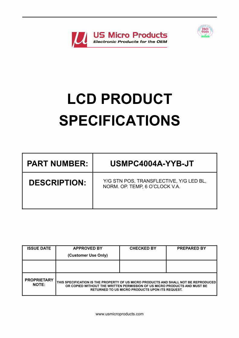
LCD PRODUCT SPECIFICATIONS
PART NUMBER: USMPC4004A-YYB-JT
DESCRIPTION:
Y/G STN POS, TRANSFLECTIVE, Y/G LED BL, NORM. OP. TEMP, 6 O’CLOCK V.A.
ISSUE DATE APPROVED BY (Customer Use Only)
CHECKED BY PREPARED BY
PROPRIETARY
NOTE:
THIS SPECIFICATION IS THE PROPERTY OF US MICRO PRODUCTS AND SHALL NOT BE REPRODUCED OR COPIED WITHOUT THE WRITTEN PERMISSION OF US MICRO PRODUCTS AND MUST BE
RETURNED TO US MICRO PRODUCTS UPON ITS REQUEST.
www.usmicroproducts.com
Contents 1.Module Classification Information
2.Precautions in use of LCD Modules
3.General Specification
4.Absolute Maximum Ratings
5.Electrical Characteristics
6.Optical Characteristics
7.Interface Pin Function
8.Contour Drawing & Block Diagram
9.Function Description
10.Character Generator ROM Pattern
11.Instruction Table
12.Timing Characteristics
13.Initializing of LCM
14.Quality Assurance
15.Reliability
16.Backlight Information
www.usmicroproducts.com Tel: 800.741.1800 2
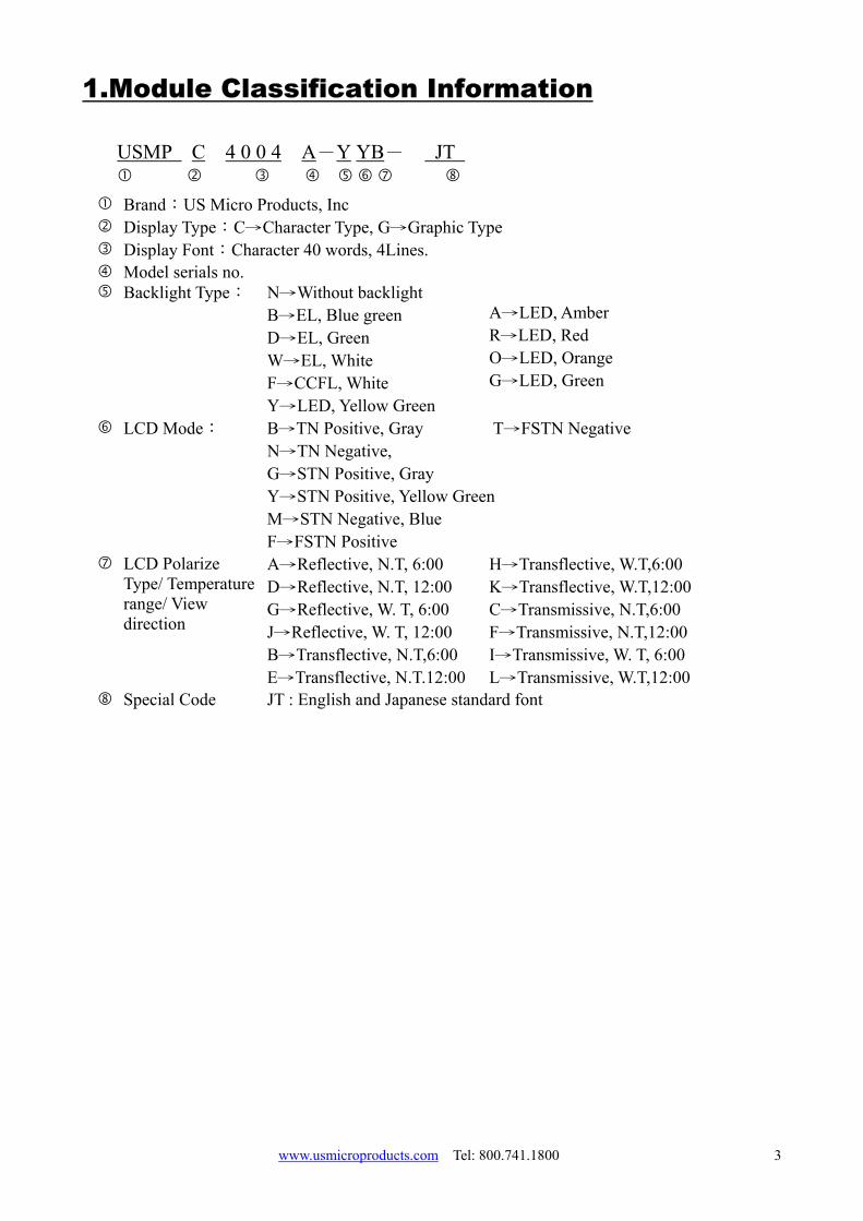
1.Module Classification Information
USMP C 4 0 0 4 A-Y YB- JT
Brand:US Micro Products, Inc Display Type:C→Character Type, G→Graphic Type Display Font:Character 40 words, 4Lines. Model serials no. Backlight Type: N→Without backlight
B→EL, Blue green D→EL, Green W→EL, White F→CCFL, White Y→LED, Yellow Green
A→LED, Amber R→LED, Red O→LED, Orange G→LED, Green
LCD Mode: B→TN Positive, Gray T→FSTN Negative N→TN Negative, G→STN Positive, Gray Y→STN Positive, Yellow Green M→STN Negative, Blue F→FSTN Positive
LCD Polarize Type/ Temperature range/ View direction
A→Reflective, N.T, 6:00 D→Reflective, N.T, 12:00 G→Reflective, W. T, 6:00 J→Reflective, W. T, 12:00 B→Transflective, N.T,6:00 E→Transflective, N.T.12:00
H→Transflective, W.T,6:00 K→Transflective, W.T,12:00 C→Transmissive, N.T,6:00 F→Transmissive, N.T,12:00 I→Transmissive, W. T, 6:00 L→Transmissive, W.T,12:00
Special Code JT : English and Japanese standard font
www.usmicroproducts.com Tel: 800.741.1800 3
2.Precautions in use of LCD Modules
(1)Avoid applying excessive shocks to the module or making any alterations or modifications to it.
(2)Don’t make extra holes on the printed circuit board, modify its shape or change the components of LCD module.
(3)Don’t disassemble the LCM. (4)Don’t operate it above the absolute maximum rating. (5)Don’t drop, bend or twist LCM. (6)Soldering: only to the I/O terminals. (7)Storage: please storage in anti-static electricity container and clean environment.
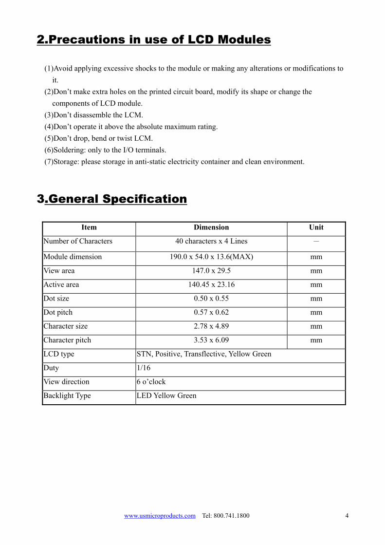
3.General Specification
Item Dimension Unit
Number of Characters 40 characters x 4 Lines -
Module dimension 190.0 x 54.0 x 13.6(MAX) mm
View area 147.0 x 29.5 mm
Active area 140.45 x 23.16 mm
Dot size 0.50 x 0.55 mm
Dot pitch 0.57 x 0.62 mm
Character size 2.78 x 4.89 mm
Character pitch 3.53 x 6.09 mm
LCD type STN, Positive, Transflective, Yellow Green
Duty 1/16
View direction 6 o’clock
Backlight Type LED Yellow Green
www.usmicroproducts.com Tel: 800.741.1800 4
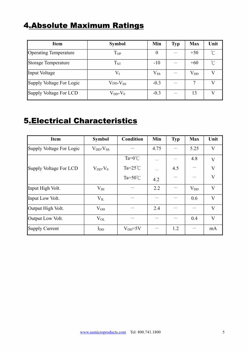
4.Absolute Maximum Ratings
Item Symbol Min Typ Max Unit
Operating Temperature TOP 0 - +50 ℃
Storage Temperature TST -10 - +60 ℃
Input Voltage VI VSS - VDD V
Supply Voltage For Logic VDD-VSS -0.3 - 7 V
Supply Voltage For LCD VDD-V0 -0.3 - 13 V
5.Electrical Characteristics
Item Symbol Condition Min Typ Max Unit
Supply Voltage For Logic VDD-VSS - 4.75 - 5.25 V
Supply Voltage For LCD VDD-V0
Ta=0℃
Ta=25℃
Ta=50℃
-
-
4.2
-
4.5
-
4.8
-
-
V
V
V
Input High Volt. VIH - 2.2 - VDD V
Input Low Volt. VIL - - - 0.6 V
Output High Volt. VOH - 2.4 - - V
Output Low Volt. VOL - - - 0.4 V
Supply Current IDD VDD=5V - 1.2 - mA
www.usmicroproducts.com Tel: 800.741.1800 5
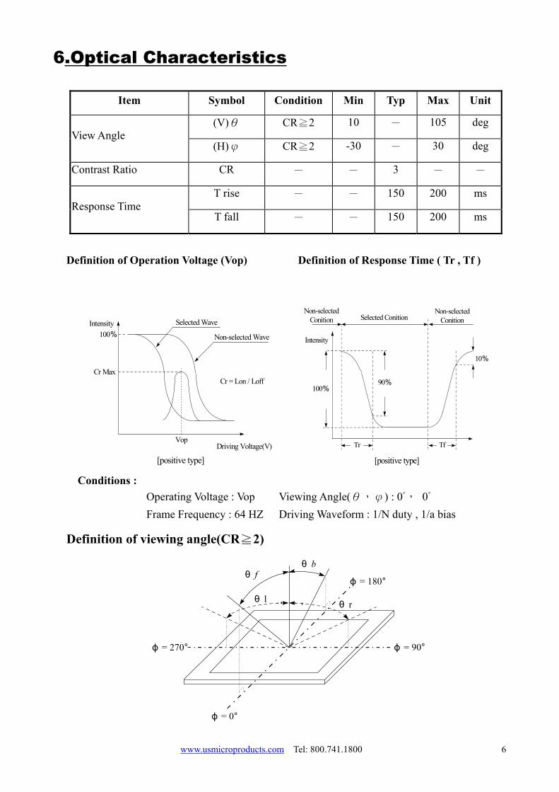
6.Optical Characteristics
Item Symbol Condition Min Typ Max Unit
(V)θ CR≧2 10 - 105 deg View Angle
(H)φ CR≧2 -30 - 30 deg
Contrast Ratio CR - - 3 - -
T rise - - 150 200 ms Response Time
T fall - - 150 200 ms
Definition of Operation Voltage (Vop) Definition of Response Time ( Tr , Tf )
Driving Voltage(V)
Intensity
Cr Max
100%
Vop
Selected Wave
Non-selected Wave
[positive type]
Cr = Lon / Loff
Intensity
90%100%
Tr
10%
Tf
Non-selectedConition
Non-selectedConitionSelected Conition
[positive type] Conditions : Operating Voltage : Vop Viewing Angle(θ,φ) : 0°, 0° Frame Frequency : 64 HZ Driving Waveform : 1/N duty , 1/a bias
Definition of viewing angle(CR≧2)
θ fφ = 180°
φ = 90°
φ = 0°
φ = 270°
θ b
θ rθ l
www.usmicroproducts.com Tel: 800.741.1800 6
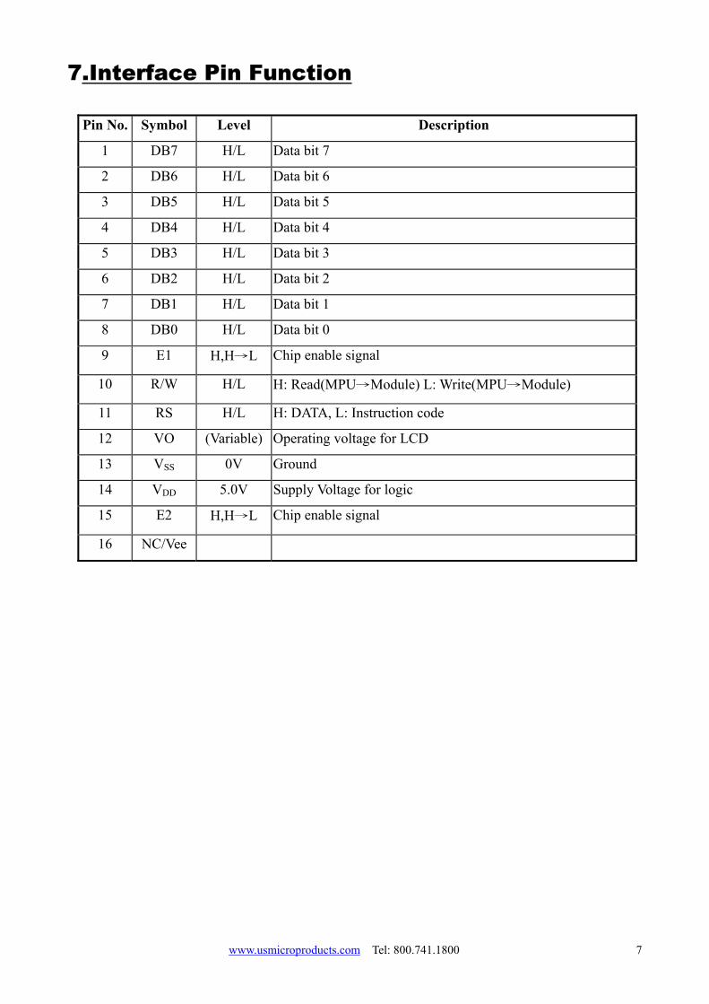
7.Interface Pin Function
Pin No. Symbol Level Description
1 DB7 H/L Data bit 7
2 DB6 H/L Data bit 6
3 DB5 H/L Data bit 5
4 DB4 H/L Data bit 4
5 DB3 H/L Data bit 3
6 DB2 H/L Data bit 2
7 DB1 H/L Data bit 1
8 DB0 H/L Data bit 0
9 E1 H,H→L Chip enable signal
10 R/W H/L H: Read(MPU→Module) L: Write(MPU→Module)
11 RS H/L H: DATA, L: Instruction code
12 VO (Variable) Operating voltage for LCD
13 VSS 0V Ground
14 VDD 5.0V Supply Voltage for logic
15 E2 H,H→L Chip enable signal
16 NC/Vee
www.usmicroproducts.com Tel: 800.741.1800 7
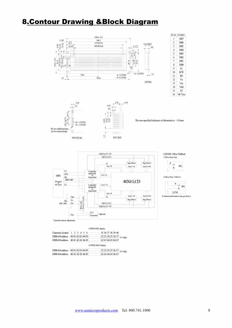
8.Contour Drawing &Block Diagram
The non-specified tolerance of dimension is 0.3mm.
RS Equivalent
0545
ControllerHD44780 Equivalent
External contrast adjustment.
4505
DDRAM addressDDRAM address
DDRAM addressDDRAM address
0040
4000 01 02 03 04
41 42 4443
0141 42
02 044443
03Character located
80 series68 series
Bia
s and
Pow
er C
ircui
t
Vee
1 2 3 54 6
DB0~DB7
VddVoVss10K~20K
VR
orE2
E1=High
E2=High
2363
63
LOWER 40X2 display
232262
6222
2524 272664 65 6766
6424
6525 27
676626
Vdd,Vss,V1~V5
36
Optional
UPPER 40X2 display
35
GeneratorN.V.
37 38 4039
Com17~32
M,CL1,CL2
or
Seg1~40
D
40X4 LCD
Seg DriverSeg41~120
Seg DriverSeg120~200
23.1
6(A
A)
29.5
(VA
)41
.954
.00.
5
7.0
21.0
47.0
K
ControllerHD44780
183.095.0
(P2.
54*7
)17
.78
The two additional pinsare for custom design.
MPU
E1R/W
PIN DETAIL
16- 1.0 PTH16- 1.8 PAD
18.1
1
2.52.54
3.5
15 16
0.55
0.62
4.89
DOT SIZE
Vdd,Vss,V1~V5M,CL1,CL2
Com1~16or
DSeg1~40
1.2
Seg DriverSeg41~120
Seg DriverSeg120~200
0.75
4- 3.5 PTH4- 6.5 PAD
0.572.78
0.5
4- 1.0 PTH
LED B/L
1.6
140.45(AA)147.0(VA)
166.3190.0 0.5
15.4
212
.25
24.7821.5
6.05
11.85
1 2
3.5
23.5
2.5
A
16.5
9.013.6 MAX
(Contrast performance may go down.)LCM
AK
RB/L
LED B/L Drive Method
2.Drive from Vdd,Vss
1.Drive from A,K
RB/L
KA
NC/Vee16
VddVss
15141312
E2
Vo
R/W111098
RS
E1DB0
DB44
DB2DB3
765
DB1
DB7
DB5DB62
3
1
www.usmicroproducts.com Tel: 800.741.1800 8
9.Function Description
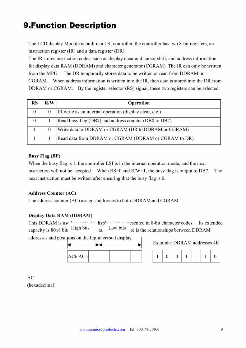
The LCD display Module is built in a LSI controller, the controller has two 8-bit registers, an instruction register (IR) and a data register (DR). The IR stores instruction codes, such as display clear and cursor shift, and address information for display data RAM (DDRAM) and character generator (CGRAM). The IR can only be written from the MPU. The DR temporarily stores data to be written or read from DDRAM or CGRAM. When address information is written into the IR, then data is stored into the DR from DDRAM or CGRAM. By the register selector (RS) signal, these two registers can be selected.
RS R/W Operation
0 0 IR write as an internal operation (display clear, etc.)
0 1 Read busy flag (DB7) and address counter (DB0 to DB7)
1 0 Write data to DDRAM or CGRAM (DR to DDRAM or CGRAM)
1 1 Read data from DDRAM or CGRAM (DDRAM or CGRAM to DR)
Busy Flag (BF)
When the busy flag is 1, the controller LSI is in the internal operation mode, and the next instruction will not be accepted. When RS=0 and R/W=1, the busy flag is output to DB7. The next instruction must be written after ensuring that the busy flag is 0.
Address Counter (AC) The address counter (AC) assigns addresses to both DDRAM and CGRAM Display Data RAM (DDRAM) This DDRAM is used to store the display data represented in 8-bit character codes. Its extended capacity is 80×8 bits or 80 characters. Below figure is the relationships between DDRAM addresses and positions on the liquid crystal display.
High bits Low bits
AC (hexadecimal)
Example: DDRAM addresses 4E
AC6 AC5 AC4 AC3 AC2 AC1 AC0 1 0 0 1 1 1 0
www.usmicroproducts.com Tel: 800.741.1800 9
1 2 3 4 5 6 ………………… 35 36 37 38 39 40
00 01 02 03 04 05 …………. 22 23 24 25 26 27 40 41 42 43 44 45 ………….. 62 63 64 65 66 67
2-Line by 40-Character Display
Display position DDRAM address
Character Generator ROM (CGROM) The CGROM generate 5×8 dot or 5×10 dot character patterns from 8-bit character codes. See Table 2.
Character Generator RAM (CGRAM) In CGRAM, the user can rewrite character by program. For 5×8 dots, eight character patterns
can be written, and for 5×10 dots, four character patterns can be written. Write into DDRAM the character code at the addresses shown as the left column of table 1. To show the character patterns stored in CGRAM.
www.usmicroproducts.com Tel: 800.741.1800 10
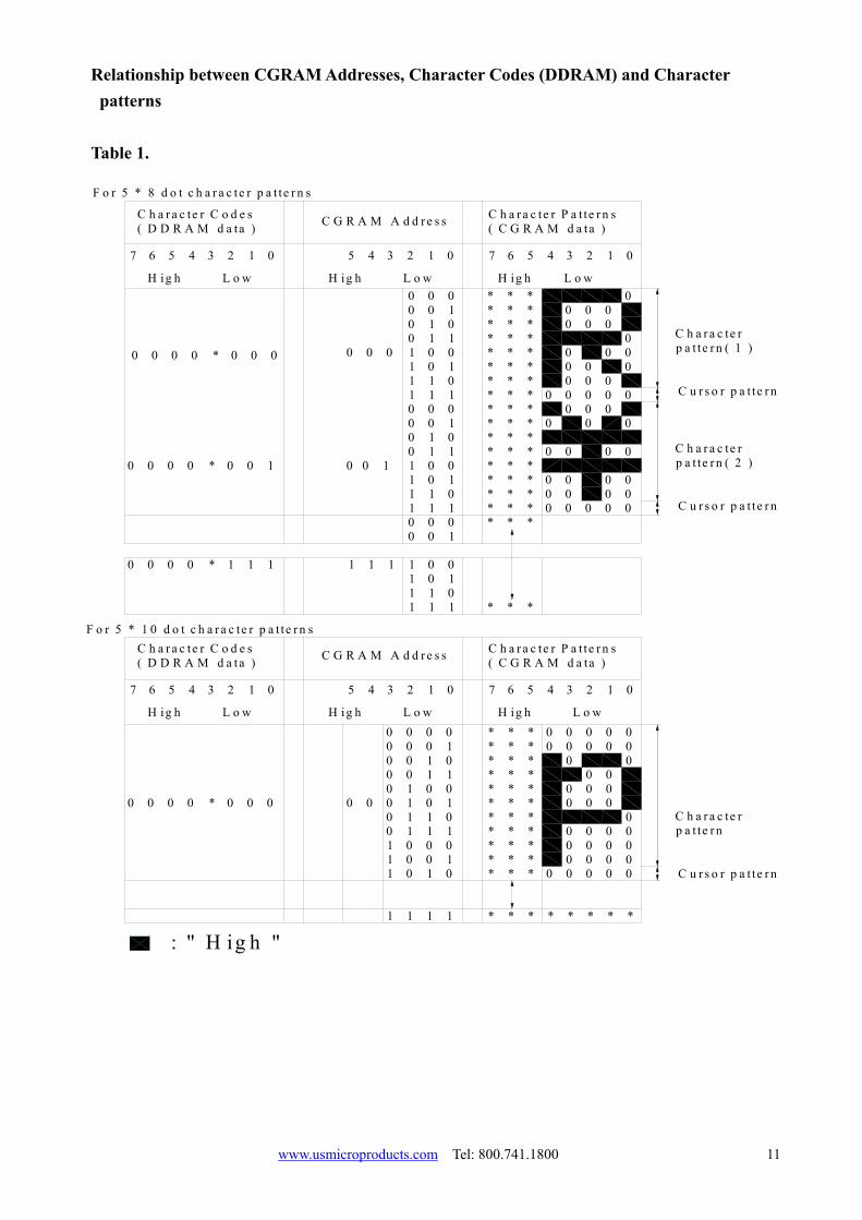
Relationship between CGRAM Addresses, Character Codes (DDRAM) and Character patterns
Table 1.
F o r 5 * 8 d o t c h a r a c te r p a t te r n s
C h a r a c te r C o d e s( D D R A M d a ta ) C G R A M A d d r e s s C h a r a c te r P a t te r n s
( C G R A M d a ta )
5 4 3 2 1 067 5 4 3 2 01 7 6 5 4 3 2 1 0
0 0 000 110 010 101 001 111 011 100 000 110 010 101 001 111 011 100 000 1
01 001 111 011 1
* * ** * ** * ** * ** * ** * ** * ** * * 0 0 0 0 0* * ** * ** * ** * ** * ** * ** * ** * * 0 0 0 0 0
0 0 0 00 0 0 0
0 0 0 0
0 0 00 0 0
0 0 00 0 00 0 0
00 0 00 0 0
0
0 0 0
00 1
* * *
* * *
1 1 10 0 0 0 * 1 1 1
0 0 0 0 * 0 0 0
0 0 0 0 * 0 0 1
H ig h L o w H ig h L o w H ig h L o w
F o r 5 * 1 0 d o t c h a r a c te r p a t te r n sC h a r a c te r C o d e s( D D R A M d a ta ) C G R A M A d d r e s s C h a r a c te r P a t te r n s
( C G R A M d a ta )
7
H ig h L o w
456 3 2 1 0
H ig h L o w
5 4 3 2 1 0
H ig h L o w
7 6 5 4 123 0
* * * 0 0 0 0 00 0 0 0 0* * *
* * ** * ** * ** * ** * ** * ** * ** * ** * *
* * * * * * * *
0 0 0 00 0 0 10 0 1 00 0 1 10 1 0 00 1 0 10 1 1 00 1 1 11 0 0 01 0 0 11 0 1 0
1 1 1 1
0 0 0 0 0
0 0 0 0 * 0 0 0 0 0
0 00 0
0 0 00 0 0
00 0 0 00 0 0 00 0 0 0
C h a r a c te rp a t te r n ( 1 )
C u r s o r p a t te r n
C h a r a c te rp a t te r n ( 2 )
C u r s o r p a t te r n
C h a r a c te rp a t te r n
C u r s o r p a t te r n
: " H ig h "
www.usmicroproducts.com Tel: 800.741.1800 11
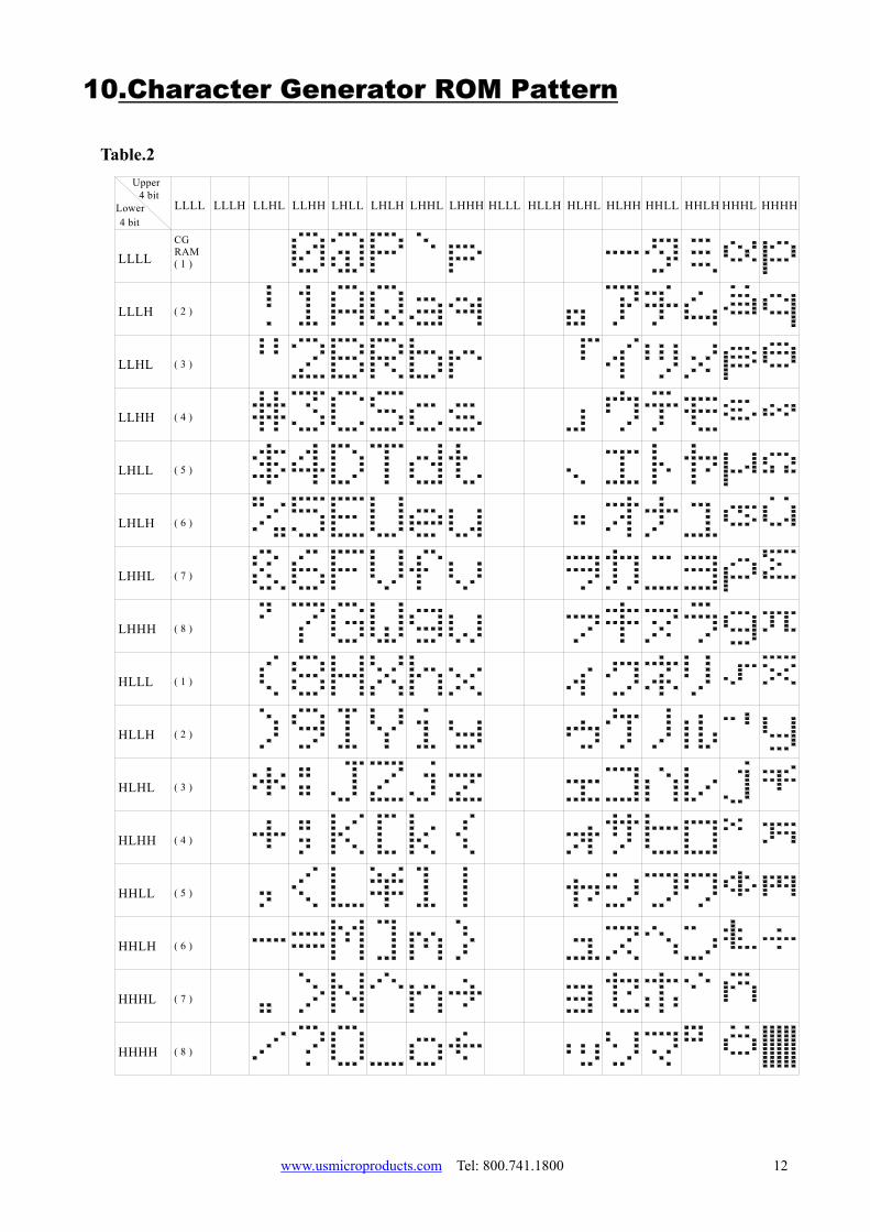
10.Character Generator ROM Pattern
Table.2
LLLL LLLH LLHL LLHH LHLL LHLH LHHL LHHH HLLL HLLH HLHL HLHH HHLL HHLH HHHL
Upper4 bit
Lower4 bit
LLLL
LLLH
LLHL
LLHH
LHLL
LHLH
LHHL
LHHH
HLLL
HLLH
HLHL
HLHH
HHLL
HHLH
HHHL
HHHH
HHHH
CGRAM( 1 )
( 2 )
( 3 )
( 4 )
( 5 )
( 6 )
( 7 )
( 8 )
( 1 )
( 2 )
( 3 )
( 4 )
( 5 )
( 6 )
( 7 )
( 8 )
www.usmicroproducts.com Tel: 800.741.1800 12
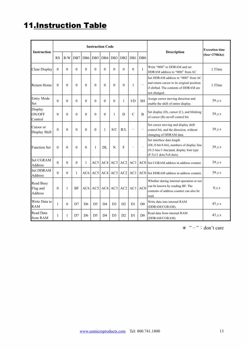
11.Instruction Table
Instruction Code Instruction
RS R/W DB7 DB6 DB5 DB4 DB3 DB2 DB1 DB0Description Execution time
(fosc=270Khz)
Clear Display 0 0 0 0 0 0 0 0 0 1 Write “00H” to DDRAM and set DDRAM address to “00H” from AC
1.53ms
Return Home 0 0 0 0 0 0 0 0 1 -
Set DDRAM address to “00H” from AC and return cursor to its original position if shifted. The contents of DDRAM are not changed.
1.53ms
Entry Mode Set
0 0 0 0 0 0 0 1 I/D SH Assign cursor moving direction and enable the shift of entire display.
39μs
Display ON/OFF Control
0 0 0 0 0 0 1 D C B Set display (D), cursor (C), and blinking of cursor (B) on/off control bit.
39μs
Cursor or Display Shift
0 0 0 0 0 1 S/C R/L - - Set cursor moving and display shift control bit, and the direction, without changing of DDRAM data.
39μs
Function Set 0 0 0 0 1 DL N F - -
Set interface data length (DL:8-bit/4-bit), numbers of display line (N:2-line/1-line)and, display font type (F:5×11 dots/5×8 dots)
39μs
Set CGRAM Address
0 0 0 1 AC5 AC4 AC3 AC2 AC1 AC0 Set CGRAM address in address counter. 39μs
Set DDRAM Address
0 0 1 AC6 AC5 AC4 AC3 AC2 AC1 AC0 Set DDRAM address in address counter. 39μs
Read Busy Flag and Address
0 1 BF AC6 AC5 AC4 AC3 AC2 AC1 AC0
Whether during internal operation or not can be known by reading BF. The contents of address counter can also be read.
0μs
Write Data to RAM
1 0 D7 D6 D5 D4 D3 D2 D1 D0 Write data into internal RAM (DDRAM/CGRAM).
43μs
Read Data from RAM
1 1 D7 D6 D5 D4 D3 D2 D1 D0 Read data from internal RAM (DDRAM/CGRAM).
43μs
* ”-”:don’t care
www.usmicroproducts.com Tel: 800.741.1800 13
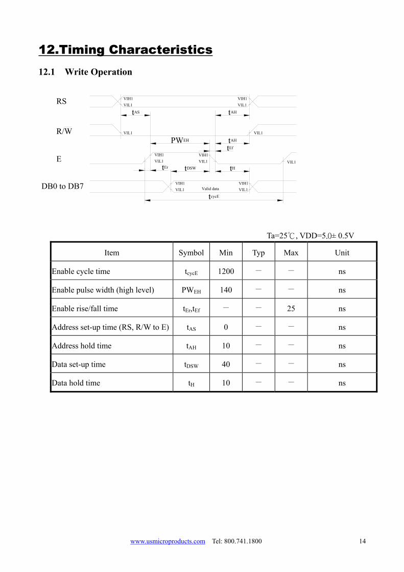
12.Timing Characteristics 12.1 Write Operation
VIH1VIL1
VIH1VIL1
VIL1
tcycE
VIH1VIL1
VIH1VIL1
VIL1
tAS tAH
tAH
tEf
tHtDSW
PWEH
tErVIL1
VIH1VIL1
VIH1VIL1
RS
R/W
E
DB0 to DB7 Valid data
Ta=25℃, VDD=5.0± 0.5V
Item Symbol Min Typ Max Unit
Enable cycle time tcycE 1200 - - ns
Enable pulse width (high level) PWEH 140 - - ns
Enable rise/fall time tEr,tEf - - 25 ns
Address set-up time (RS, R/W to E) tAS 0 - - ns
Address hold time tAH 10 - - ns
Data set-up time tDSW 40 - - ns
Data hold time tH 10 - - ns
www.usmicroproducts.com Tel: 800.741.1800 14
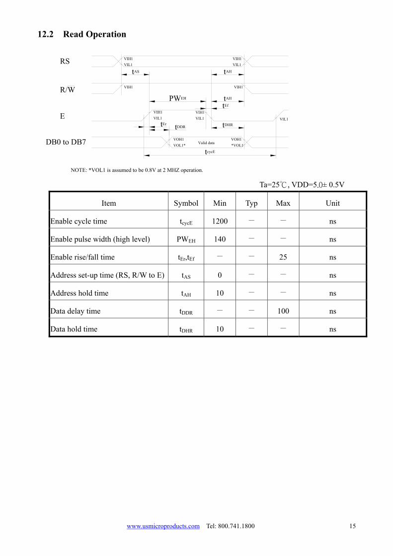
12.2 Read Operation
VIH1VIL1
VIH1VIL1
tcycE
VOH1VOL1*
tAS tAH
tAH
tEf
tDHR
PWEH
tErVIL1
VIH1VIL1
VIH1VIL1
RS
R/W
E
DB0 to DB7
VIH1 VIH1
VOH1*VOL1Valid data
tDDR
NOTE: *VOL1 is assumed to be 0.8V at 2 MHZ operation.
Ta=25℃, VDD=5.0± 0.5V
Item Symbol Min Typ Max Unit
Enable cycle time tcycE 1200 - - ns
Enable pulse width (high level) PWEH 140 - - ns
Enable rise/fall time tEr,tEf - - 25 ns
Address set-up time (RS, R/W to E) tAS 0 - - ns
Address hold time tAH 10 - - ns
Data delay time tDDR - - 100 ns
Data hold time tDHR 10 - - ns
www.usmicroproducts.com Tel: 800.741.1800 15
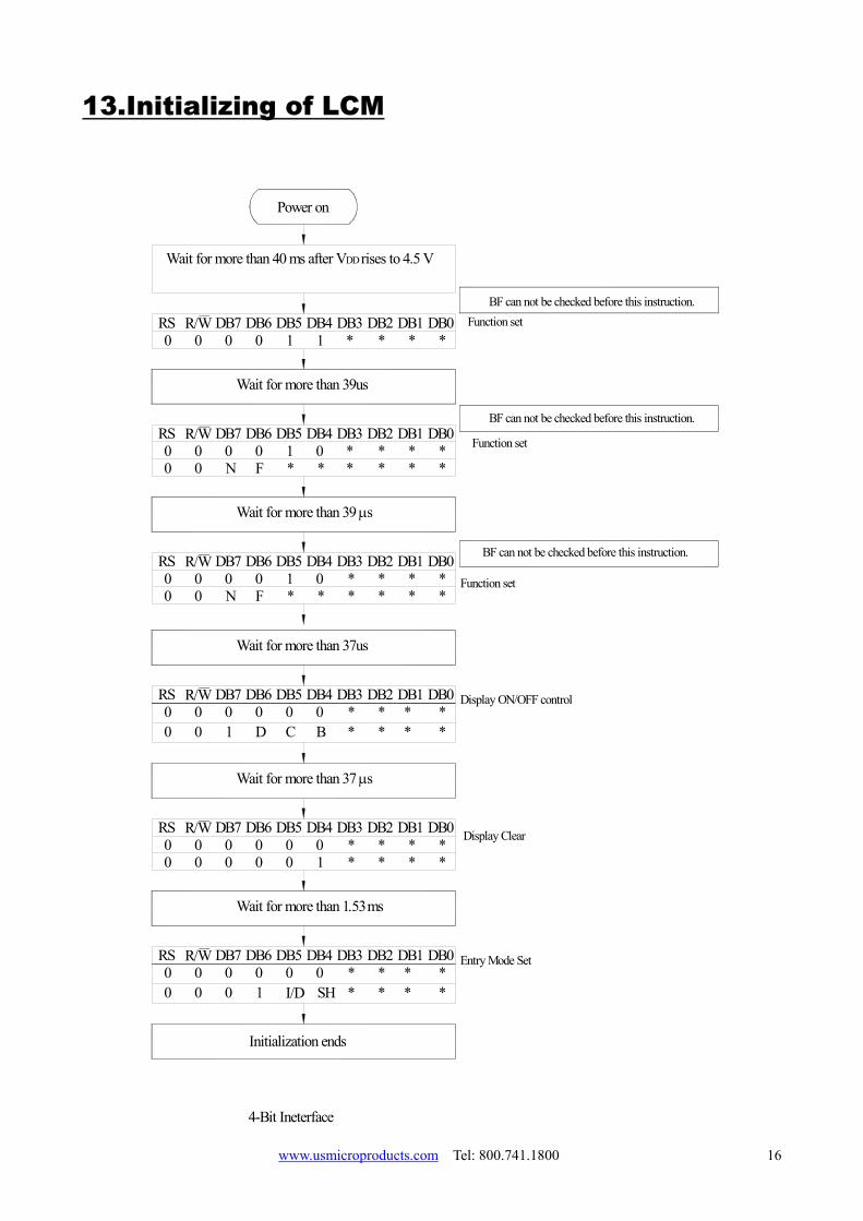
13.Initializing of LCM
0
R/W
00
R/W
00
R/W
0
0
0
0
0R/W
0R/W
Wait for more than 40 ms after VDD rises to 4.5 V
R/W
0
RS
RS0
00
RS00
0
RS0
00
RS
RS0
Display Clear
Entry Mode Set
Display ON/OFF control
4-Bit Ineterface
Initialization ends
0 1 SHI/D * ** *
Wait for more than 37 µs
DB3
Wait for more than 1.53ms
DB3
DB3
DB4DB6DB7 DB5
DB5DB70
DB60
00
00
DB400 *
010
0**
DB5DB701
0D
DB6
B0
DB40C
**
DB2 DB1 DB0*
DB0*
*
DB1DB2* *
**
**
**
DB0DB1**
DB2**
BF can not be checked before this instruction.
BF can not be checked before this instruction.
Function set
Function set BF can not be checked before this instruction.
Wait for more than 37us
DB3
Wait for more than 39 µs
DB3
Wait for more than 39us
DB5
FN
DB70
DB60
** *0
DB41 *
DB50 0N F
DB7 DB6*1 0
** *
DB4
**
DB0
**
DB1DB2* * Function set
*
DB0***
* *
DB1DB2
DB3DB5DB70 0
DB61
DB41 *
Power on
*DB0DB1
*DB2
*
www.usmicroproducts.com Tel: 800.741.1800 16
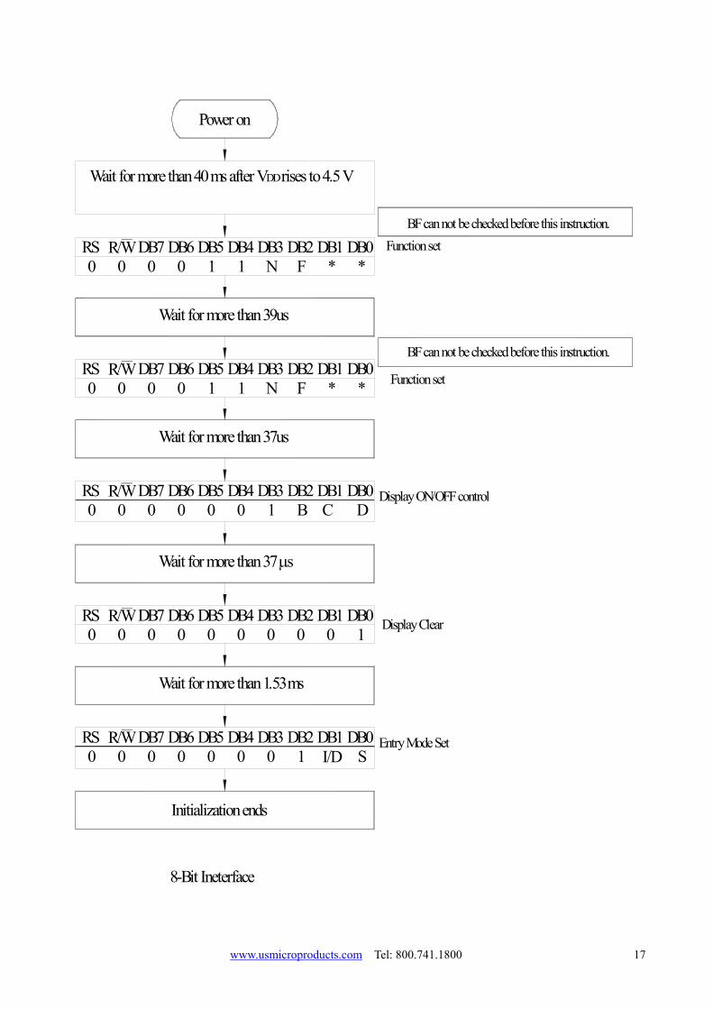
Power on
RS R/WDB7 DB6 DB5 DB4 DB3 DB2 DB1 DB0
Wait for more than 40 ms after VDD rises to 4.5 V
Wait for more than 39us
1DB4DB6
0DB5
1DB1DB2DB3
F * *DB0
DB4DB7RS R/W DB6 DB5 DB1DB2DB3 DB00 0 0 0 0 0 1 B C D
Initialization ends
BF can not be checked before this instruction.Function set
Function set
BF can not be checked before this instruction.
8-Bit Ineterface
Wait for more than 37us
Display ON/OFF control
00 0 0 11 *F *
00 0
R/W0
R/W0
0RS
RS0
Entry Mode Set DB3
Wait for more than 1.53ms
00 000DB5DB7 DB6 DB4
I/D1 SDB0DB1DB2
Display Clear DB3
Wait for more than 37 µs
DB5DB70 0
DB6 DB400 0
DB01
DB10
DB20
RS R/WDB7
N
N
www.usmicroproducts.com Tel: 800.741.1800 17
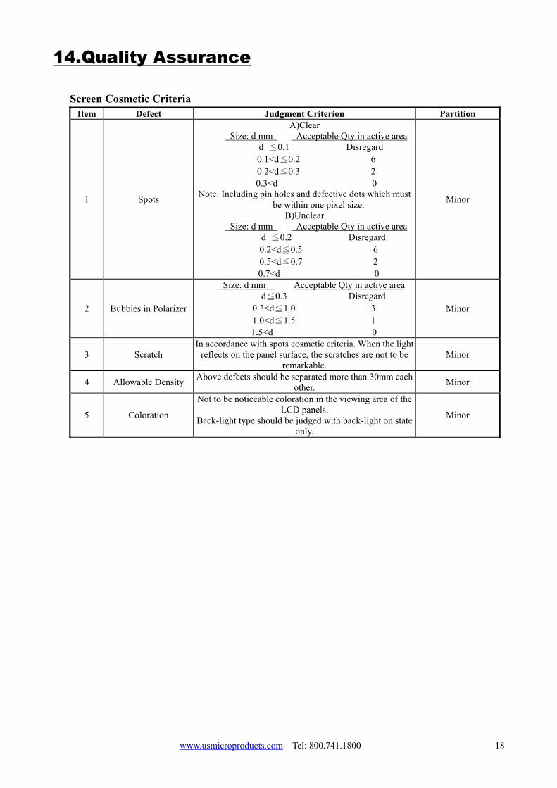
14.Quality Assurance
Screen Cosmetic Criteria Item Defect Judgment Criterion Partition
1 Spots
A)Clear Size: d mm Acceptable Qty in active area
d ≦0.1 Disregard 0.1<d≦0.2 6 0.2<d≦0.3 2 0.3<d 0
Note: Including pin holes and defective dots which must be within one pixel size.
B)Unclear Size: d mm Acceptable Qty in active area
d ≦0.2 Disregard 0.2<d≦0.5 6 0.5<d≦0.7 2 0.7<d 0
Minor
2 Bubbles in Polarizer
Size: d mm Acceptable Qty in active area d≦0.3 Disregard
0.3<d≦1.0 3 1.0<d≦1.5 1 1.5<d 0
Minor
3 Scratch In accordance with spots cosmetic criteria. When the light
reflects on the panel surface, the scratches are not to be remarkable.
Minor
4 Allowable Density Above defects should be separated more than 30mm each other. Minor
5 Coloration
Not to be noticeable coloration in the viewing area of the LCD panels.
Back-light type should be judged with back-light on state only.
Minor
www.usmicroproducts.com Tel: 800.741.1800 18
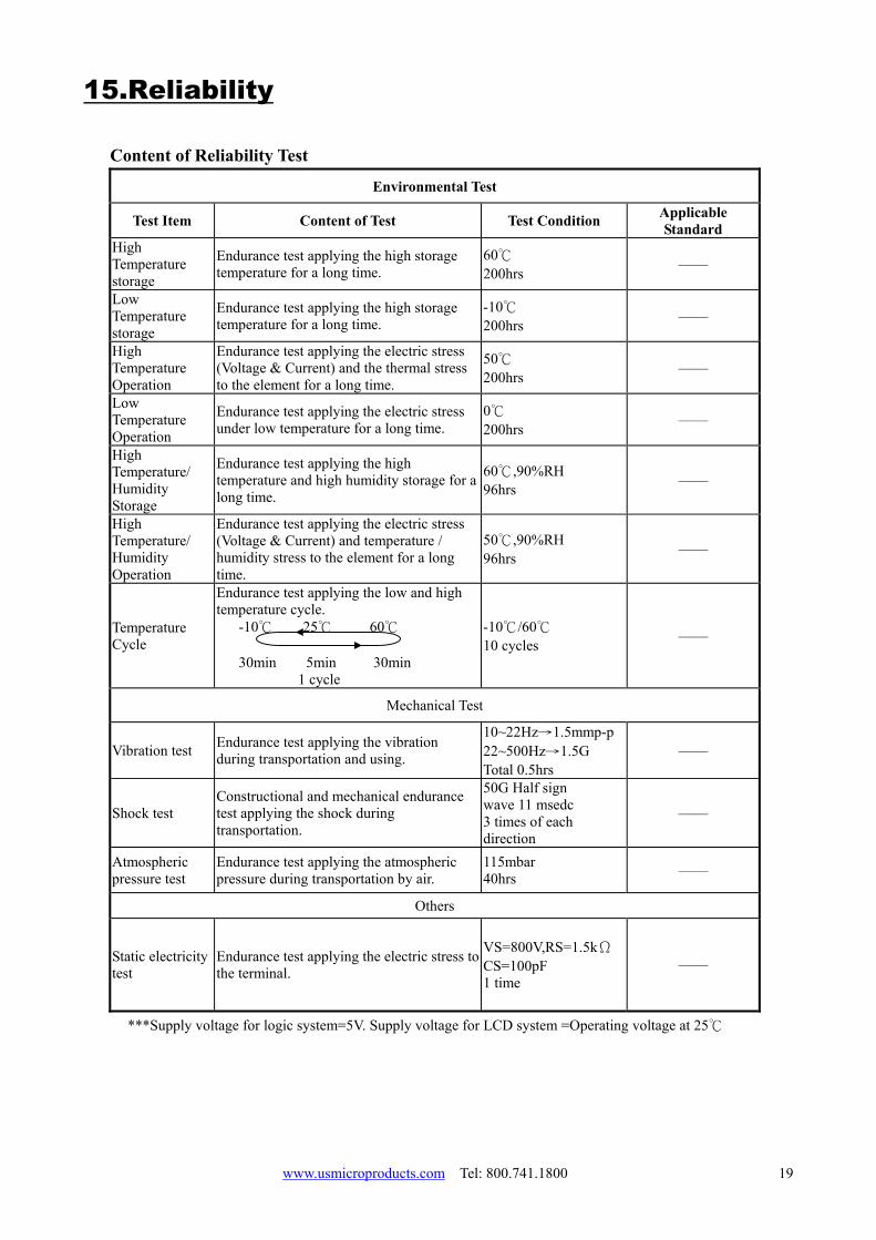
15.Reliability Content of Reliability Test
Environmental Test
Test Item Content of Test Test Condition Applicable Standard
High Temperature storage
Endurance test applying the high storage temperature for a long time.
60℃ 200hrs ——
Low Temperature storage
Endurance test applying the high storage temperature for a long time.
-10℃ 200hrs ——
High Temperature Operation
Endurance test applying the electric stress (Voltage & Current) and the thermal stress to the element for a long time.
50℃ 200hrs ——
Low Temperature Operation
Endurance test applying the electric stress under low temperature for a long time.
0℃ 200hrs ——
High Temperature/ Humidity Storage
Endurance test applying the high temperature and high humidity storage for a long time.
60℃,90%RH 96hrs ——
High Temperature/ Humidity Operation
Endurance test applying the electric stress (Voltage & Current) and temperature / humidity stress to the element for a long time.
50℃,90%RH 96hrs ——
Temperature Cycle
Endurance test applying the low and high temperature cycle. -10℃ 25℃ 60℃ 30min 5min 30min 1 cycle
-10℃/60℃ 10 cycles ——
Mechanical Test
Vibration test Endurance test applying the vibration during transportation and using.
10~22Hz→1.5mmp-p 22~500Hz→1.5G Total 0.5hrs
——
Shock test Constructional and mechanical endurance test applying the shock during transportation.
50G Half sign wave 11 msedc 3 times of each direction
——
Atmospheric pressure test
Endurance test applying the atmospheric pressure during transportation by air.
115mbar 40hrs ——
Others
Static electricity test
Endurance test applying the electric stress to the terminal.
VS=800V,RS=1.5kΩ CS=100pF 1 time
——
***Supply voltage for logic system=5V. Supply voltage for LCD system =Operating voltage at 25℃
www.usmicroproducts.com Tel: 800.741.1800 19
www.usmicroproducts.com Tel: 800.741.1800 20
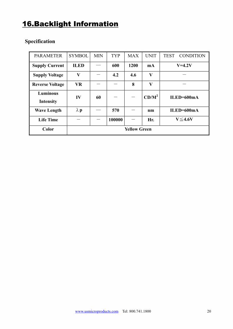
16.Backlight Information
Specification
PARAMETER SYMBOL MIN TYP MAX UNIT TEST CONDITION
Supply Current ILED ― 600 1200 mA V=4.2V
Supply Voltage V - 4.2 4.6 V -
Reverse Voltage VR - - 8 V -
Luminous
Intensity IV 60 - - CD/M2 ILED=600mA
Wave Length λp ― 570 - nm ILED=600mA
Life Time - - 100000 - Hr. V≦4.6V
Color Yellow Green