Embed Size (px)
Citation preview

1 Publication Order Number : LE25U40CMC/D
www.onsemi.com
© Semiconductor Components Industries, LLC, 2016 February 2016 - Rev. 1
ORDERING INFORMATION See detailed ordering and shipping information on page 24 of this data sheet.
LE25U40CMC CMOS LSI
Serial Flash Memory, 4 Mb (512K8)
Overview The LE25U40CMC is a SPI bus flash memory device with a 4M bit (512K 8-bit) configuration that adds a high performance Dual output and Dual I/O function. It uses a single 2.5v power supply. While making the most of the features inherent to a serial flash memory device, the LE25U40CMC is housed in an 8-pin ultra-miniature package. All these features make this device ideally suited to storing program in applications such as portable information devices, which are required to have increasingly more compact dimensions. The LE25U40CMC also has a small sector erase capability which makes the device ideal for storing parameters or data that have fewer rewrite cycles and conventional EEPROMs cannot handle due to insufficient capacity.
Features Read/write operations enabled by single 2.5v power supply: 2.3 to 3.6V supply voltage range Operating frequency : 40MHz Temperature range : 40 to 85C Serial interface : SPI mode 0, mode 3 supported / Dual Output, Dual I/O supported Sector size : 4K bytes/small sector, 64K bytes/sector Small sector erase, sector erase, chip erase functions Page program function (256 bytes / page) Block protect function Highly reliable read/write
Number of rewrite times : 100,000 times Small sector erase time : 40ms (typ.), 150ms (max.) Sector erase time : 80ms (typ.), 250ms (max.) Chip erase time : 250ms (typ.), 2.0s (max.) Page program time : 4.0ms/256 bytes (typ.), 5.0ms/256 bytes (max.)
Status functions : Ready/busy information, protect information Data retention period : 20 years Package : SOP8J (200mil)
* This product is licensed from Silicon Storage Technology, Inc. (USA).
SOIC-8 / SOP8J (200mil)
LE25U40CMC
www.onsemi.com 2
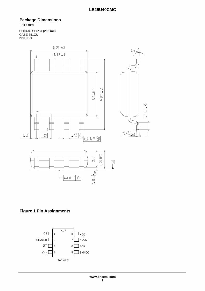
Package Dimensions unit : mm
Figure 1 Pin Assignments
SOIC-8 / SOP8J (200 mil)CASE 751CUISSUE O
to
Top view
CS
SO/SIO1
WP
VSS
VDD
HOLD
SCK
SI/SIO0
1
2
3
4
8
7
6
5

LE25U40CMC
www.onsemi.com 3
Figure 2 Block Diagram
Table 1 Pin Description
Symbol Pin Name Description
SCK Serial clock This pin controls the data input/output timing.
The input data and addresses are latched synchronized to the rising edge of the serial clock, and the data is
output synchronized to the falling edge of the serial clock.
SI/SIO0 Serial data input
/ Serial data input output
The data and addresses are input from this pin, and latched internally synchronized to the rising edge of the
serial clock. It changes into the output pin at Dual Output and it changes into the input output pin at Dual I/O.
SO/SIO1 Serial data input
/ Serial data input output
The data stored inside the device is output from this pin synchronized to the falling edge of the serial clock.
It changes into the output pin at Dual Output and it changes into the input output pin at Dual I/O.
CS Chip select The device becomes active when the logic level of this pin is low; it is deselected and placed in standby
status when the logic level of the pin is high.
WP Write protect The status register write protect (SRWP) takes effect when the logic level of this pin is low.
HOLD Hold Serial communication is suspended when the logic level of this pin is low.
VDD Power supply This pin supplies the 2.3 to 3.6V supply voltage.
VSS Ground This pin supplies the 0V supply voltage.
4M Bit Flash EEPROM
Cell Array
Y-DECODER
I/O BUFFERS &
DATA LATCHES
CS SCK SI/SIO0 HOLD WP SO/SIO1
X- DECODER ADDRESS
BUFFERS &
LATCHES
SERIAL INTERFACE
CONTROL LOGIC

LE25U40CMC
www.onsemi.com 4
Device Operation The read, erase, program and other required functions of the device are executed through the command registers. The serial I/O corrugate is shown in Figure 3 and the command list is shown in Table 2. At the falling CS edge the device is selected, and serial input is enabled for the commands, addresses, etc. These inputs are normalized in 8 bit units and taken into the device interior in synchronization with the rising edge of SCK, which causes the device to execute operation according to the command that is input. The LE25U40CMC supports both serial interface SPI mode 0 and SPI mode 3. At the falling CS edge, SPI mode 0 is automatically selected if the logic level of SCK is low, and SPI mode 3 is automatically selected if the logic level of SCK is high.
Figure 3 I/O waveforms
Table 2 Command Settings
Command 1st bus cycle 2nd bus cycle 3rd bus cycle 4th bus cycle 5th bus cycle 6th bus cycle Nth bus cycle
Read 03h A23-A16 A15-A8 A7-A0 RD *1 RD *1 RD *1
High Speed Read 0Bh A23-A16 A15-A8 A7-A0 X RD *1 RD *1
Dual Read 3Bh A23-A16 A15-A8 A7-A0 Z RD *1 RD *1
Dual I/O Read BBh A23-A8 A7-A0,X, Z RD *1 RD *1 RD *1 RD *1
Small sector erase 20h / D7h A23-A16 A15-A8 A7-A0
Sector erase D8h A23-A16 A15-A8 A7-A0
Chip erase 60h / C7h
Page program 02h A23-A16 A15-A8 A7-A0 PD *2 PD *2 PD *2
Write enable 06h
Write disable 04h
Power down B9h
Status register read 05h
Status register write 01h DATA
JEDEC ID read 9Fh
ID read ABh X X X
power down B9h
Exit power down mode ABh
Explanatory notes for Table 2 "X" signifies "don't care" (that is to say, any value may be input)., "Z” signifies " High Impedance ". The "h" following each code indicates that the number given is in hexadecimal notation. Addresses A23 to A19 for all commands are "Don't care". *1: "RD" stands for read data. *2: "PD" stands for page program data.
CS
SCK
SO
SI
High Impedance DATA DATA
1st bus 2nd bus
8CLK
Mode0
Mode3
Nth bus
MSB (Bit7)
LSB (Bit0)

LE25U40CMC
www.onsemi.com 5
Table 3 Command Settings
4M Bit
sector(64KB) small sector address space(A23 to A0)
7 127 07F000h 07FFFFh to
112 070000h 070FFFh
6 111 06F000h 06FFFFh to 96 060000h 060FFFh
5 95 05F000h 05FFFFh to 80 050000h 050FFFh
4 79 04F000h 04FFFFh to 64 040000h 040FFFh
3 63 03F000h 03FFFFh to 48 030000h 030FFFh
2 47 02F000h 02FFFFh to 32 020000h 020FFFh
1 31 01F000h 01FFFFh to 16 010000h 010FFFh
0
15 00F000h 00FFFFh to 2 002000h 002FFFh 1 001000h 001FFFh 0 000000h 000FFFh

LE25U40CMC
www.onsemi.com 6
Description of Commands and Their Operations A detailed description of the functions and operations corresponding to each command is presented below. 1. Standard SPI read
There are two read commands, the standard SPI read command and High-speed read command. 1-1. Read command
Consisting of the first through fourth bus cycles, the 4 bus cycle read command inputs the 24-bit addresses following (03h). The data is output from SO on the falling clock edge of fourth bus cycle bit 0 as a reference. "Figure 4-a Read" shows the timing waveforms. Figure 4-a Read
1-2. High-speed Read command
Consisting of the first through fifth bus cycles, the High-speed read command inputs the 24-bit addresses and 8 dummy bits following (0Bh). The data is output from SO using the falling clock edge of fifth bus cycle bit 0 as a reference. "Figure 4-b High-speed Read" shows the timing waveforms. Figure 4-b High-speed Read
N+2 N+1 N
CS
High Impedance DATA DATA DATA
SCK
SO
SI 03h Add. Add. Add.
15
MSB MSB MSB
0 1 2 3 4 5 6 7 8 23 16 24 31 39 47
8CLK
Mode0
Mode3 32 40
N+2 N+1 N
CS
High Impedance DATA DATA DATA
SCK
SO
SI 0Bh Add. Add. Add. X
15
MSB MSB MSB
0 1 2 3 4 5 6 7 8 2316 24 31 32 39 40 47 48 55Mode3
Mode0
8CLK
MSB

LE25U40CMC
www.onsemi.com 7
2. Dual read
There are two Dual read commands, the Dual read command and the Dual I/O read command. They achieve the twice speed-up from a High-speed read command. 2-1. Dual Read command
The Dual read command changes SI/SIO0 into the output pin function in addition to SO/SIO1, makes the data output x2 bit and has achieved a high-speed output. Consisting of the first through fifth bus cycles, the Dual read command inputs the 24-bit addresses and 8 dummy bits following (3Bh). DATA1 (Bit7, BIt5, Bit3 and Bit1) is output from SI/SIO0 and DATA0 (Bit6, Bit4, Bit2 and Bit0) is output from SO/SIO1 on the falling clock edge of fifth bus cycle bit 0 as a reference. "Figure 5-a Dual Read" shows the timing waveforms. Figure 5-a Dual Read
2-2. Dual I/O Read command
The Dual I/O read command changes SI/SIO0 and SO/SIO1 into the input output pin function, makes the data input and output x2 bit and has achieved a high-speed output. Consisting of the first through third bus cycles, the Dual I/O read command inputs the 24-bit addresses and 4 dummy clocks following (BBh). The format of the address input and the dummy bit input is the x2 bit input. Add1 (A23, A21, -, A3 and A1) is input from S0/SIO1 and Add0 (A22, A20, -, A2 and A0) is input from SI/SIO0. 2CLK of the latter half of the dummy clock is in the state of high impedance, the controller can switch I/O for this period. DATA1 (Bit7, BIt5, Bit3 and Bit1) is output from SI/SIO0 and DATA0 (Bit6, Bit4, Bit2 and Bit0) is output from SO/SIO1 on the falling clock edge of third bus cycle bit 0 as a reference. "Figure 5-b Dual I/O Read" shows the timing waveforms. Figure 5-b Dual I/O Read
When SCK is input continuously after the read command has been input and the data in the designated addresses has been output, the address is automatically incremented inside the device while SCK is being input, and the corresponding data is output in sequence. If the SCK input is continued after the internal address arrives at the highest address (7FFFFh), the internal address returns to the lowest address (00000h), and data output is continued. By setting the logic level of CS to high, the device is deselected, and the read cycle ends. While the device is deselected, the output pin SO is in a high-impedance state.
CS
High Impedance DATA1 DATA1 DATA1
SCK
SO/SIO1
SI/SIO0 3Bh Add. Add. Add.
15
MSB MSB
0 1 2 3 4 5 6 7 8 23 16 24 31 32 39 40 43 44 47 Mode3
Mode0
8CL
MSB
MSB
N+2 N+1 N
DATA0 DATA0 DATA0
4CL 4CL
DATA0 b6,b4,b2,b0
DATA1 b7,b5,b3,b1
dummy bit
CS
High Impedance DATA1 DATA1 DATA1
SCK
SO/SIO1
SI/SIO0 BBh X Add1:A22,A20-A2,A0
MSB MSB
0 1 2 3 4 5 6 7 8 19 22 23 24 27 28 31Mode3
Mode0
8CL
MSB
MSB
N+2 N+1 N
DATA0 DATA0 DATA0
4CLK
DATA0 b6,b4,b2,b0
DATA1 b7,b5,b3,b1
dummy bit
20 21
Add2:A23,A21-A3,A1 X
2CLK 2CLK 12CLK
LE25U40CMC
www.onsemi.com 8
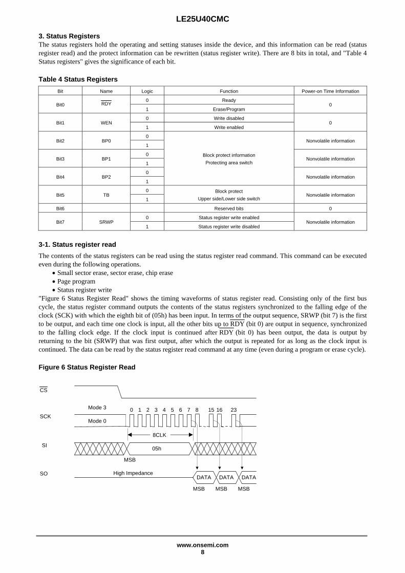
3. Status Registers The status registers hold the operating and setting statuses inside the device, and this information can be read (status register read) and the protect information can be rewritten (status register write). There are 8 bits in total, and "Table 4 Status registers" gives the significance of each bit. Table 4 Status Registers
Bit Name Logic Function Power-on Time Information
Bit0 RDY 0 Ready
0 1 Erase/Program
Bit1 WEN 0 Write disabled
0 1 Write enabled
Bit2 BP0 0
Block protect information
Protecting area switch
Nonvolatile information 1
Bit3 BP1 0
Nonvolatile information 1
Bit4 BP2 0
Nonvolatile information 1
Bit5 TB 0 Block protect
Upper side/Lower side switch Nonvolatile information
1
Bit6 Reserved bits 0
Bit7 SRWP 0 Status register write enabled
Nonvolatile information 1 Status register write disabled
3-1. Status register read
The contents of the status registers can be read using the status register read command. This command can be executed even during the following operations.
Small sector erase, sector erase, chip erase Page program Status register write
"Figure 6 Status Register Read" shows the timing waveforms of status register read. Consisting only of the first bus cycle, the status register command outputs the contents of the status registers synchronized to the falling edge of the clock (SCK) with which the eighth bit of (05h) has been input. In terms of the output sequence, SRWP (bit 7) is the first to be output, and each time one clock is input, all the other bits up to RDY (bit 0) are output in sequence, synchronized to the falling clock edge. If the clock input is continued after RDY (bit 0) has been output, the data is output by returning to the bit (SRWP) that was first output, after which the output is repeated for as long as the clock input is continued. The data can be read by the status register read command at any time (even during a program or erase cycle). Figure 6 Status Register Read
CS
SCK
SI
SO
MSB MSB MSB
05h
DATA DATA High Impedance
8 3 2 1 0 7 6 5 4 15 23Mode 3
Mode 0
8CLK
16
DATA
MSB

LE25U40CMC
www.onsemi.com 9
3-2. Status register write
The information in status registers BP0, BP1, BP2, TB and SRWP can be rewritten using the status register write command. RDY, WEN and bit 6 are read-only bits and cannot be rewritten. The information in bits BP0, BP1, BP2, TB and SRWP is stored in the non-volatile memory, and when it is written in these bits, the contents are retained even at power-down. "Figure 6 Status Register Write" shows the timing waveforms of status register write, and Figure 20 shows a status register write flowchart. Consisting of the first and second bus cycles, the status register write command initiates the internal write operation at the rising CS edge after the data has been input following (01h). Erase and program are performed automatically inside the device by status register write so that erasing or other processing is unnecessary before executing the command. By the operation of this command, the information in bits BP0, BP1, BP2, TB and SRWP can be rewritten. Since bits RDY (bit 0), WEN (bit 1) and bit 6 of the status register cannot be written, no problem will arise if an attempt is made to set them to any value when rewriting the status register. Status register write ends can be detected by RDY of status register read. To initiate status register write, the logic level of the WP pin must be set high and status register WEN must be set to "1". Figure 6 Status Register Write
3-3. Contents of each status register
RDY (Bit 0)
The RDY register is for detecting the write (program, erase and status register write) end. When it is "1", the device is in a busy state, and when it is "0", it means that write is completed. WEN (bit 1)
The WEN register is for detecting whether the device can perform write operations. If it is set to "0", the device will not perform the write operation even if the write command is input. If it is set to "1", the device can perform write operations in any area that is not block-protected. WEN can be controlled using the write enable and write disable commands. By inputting the write enable command (06h), WEN can be set to "1"; by inputting the write disable command (04h), it can be set to "0." In the following states, WEN is automatically set to "0" in order to protect against unintentional writing.
At power-on Upon completion of small sector erase, sector erase or chip erase Upon completion of page program Upon completion of status register write
* If a write operation has not been performed inside the LE25U40CMC because, for instance, the command input for any of the write operations (small sector erase, sector erase, chip erase, page program, or status register write) has failed or a write operation has been performed for a protected address, WEN will retain the status established prior to the issue of the command concerned. Furthermore, its state will not be changed by a read operation.
tSRW
Self-timed Write Cycle
SCK
SI
High Impedance SO
CS
DATA 01h
150 1 2 3 4 5 6 7 8 Mode3
Mode0
8CLK
WP
tWPH tWPS
MSB

LE25U40CMC
www.onsemi.com 10
BP0, BP1, BP2, TB (Bits 2, 3, 4, 5)
Block protect BP0, BP1, BP2 and TB are status register bits that can be rewritten, and the memory space to be protected can be set depending on these bits. For the setting conditions, refer to "Table 5 Protect level setting conditions". BP0, BP1, and BP2 are used to select the protected area and TB to allocate the protected area to the higher-order address area or lower-order address area. Table 5 Protect Level Setting Conditions
Protect Level Status Register Bits
Protected Area TB BP2 BP1 BP0
0 (Whole area unprotected) X 0 0 0 None
T1 (Upper side 1/8 protected) 0 0 0 1 07FFFFh to 070000h
T2 (Upper side 1/4 protected) 0 0 1 0 07FFFFh to 060000h
T3 (Upper side 1/2 protected) 0 0 1 1 07FFFFh to 040000h
B1 (Lower side 1/8 protected) 1 1 0 1 00FFFFh to 000000h
B2 (Lower side 1/4 protected) 1 1 1 0 01FFFFh to 000000h
B3 (Lower side 1/2 protected) 1 1 1 1 03FFFFh to 000000h
4 (Whole area protected) X 1 X X 07FFFFh to 000000h
* Chip erase is enabled only when the protect level is 0. SRWP (bit 7)
Status register write protect SRWP is the bit for protecting the status registers, and its information can be rewritten. When SRWP is "1" and the logic level of the WP pin is low, the status register write command is ignored, and status registers BP0, BP1, BP2, TB and SRWP are protected. When the logic level of the WP pin is high, the status registers are not protected regardless of the SRWP state. The SRWP setting conditions are shown in "Table 6 SRWP setting conditions". Table 6 SRWP Setting Conditions
WP Pin SRWP Status Register Protect State
0 0 Unprotected
1 Protected
1 0 Unprotected
1 Unprotected
Bit 6 are reserved bits, and have no significance.

LE25U40CMC
www.onsemi.com 11
4. Write Enable
Before performing any of the operations listed below, the device must be placed in the write enable state. Operation is the same as for setting status register WEN to "1", and the state is enabled by inputting the write enable command. "Figure 8 Write Enable" shows the timing waveforms when the write enable operation is performed. The write enable command consists only of the first bus cycle, and it is initiated by inputting (06h).
Small sector erase, sector erase, chip erase Page program Status register write
5. Write Disable
The write disable command sets status register WEN to "0" to prohibit unintentional writing. "Figure 9 Write Disable" shows the timing waveforms. The write disable command consists only of the first bus cycle, and it is initiated by inputting (04h). The write disable state (WEN "0") is exited by setting WEN to "1" using the write enable command (06h). Figure 8 Write Enable Figure 9 Write Disable 6. Power-down
The power-down command sets all the commands, with the exception of the silicon ID read command and the command to exit from power-down, to the acceptance prohibited state (power-down). "Figure 10 Power-down" shows the timing waveforms. The power-down command consists only of the first bus cycle, and it is initiated by inputting (B9h). However, a power-down command issued during an internal write operation will be ignored. The power-down state is exited using the power-down exit command (power-down is exited also when one bus cycle or more of the silicon ID read command (ABh) has been input). "Figure 11 Exiting from Power-down" shows the timing waveforms of the power-down exit command. Figure 10 Power-down Figure 11 Exiting from Power-down
SCK
SI
High Impedance SO
CS
06h
0 1 2 3 4 5 6 7 Mode3
Mode0
8CLK
SCK
SI
High Impedance SO
CS
04h
0 1 2 3 4 5 6 7 Mode3
Mode0
8CLK
MSB MSB
SCK
SI
High Impedance SO
CS
B9h
0 1 2 3 4 5 6 7 Mode3
Mode0
8CLK
SCK
SI
High Impedance SO
CS
ABh
0 1 2 3 4 5 6 7 Mode3
Mode0
8CLK
tPDR tDP
Power down mode
Power down mode
MSB MSB
LE25U40CMC
www.onsemi.com 12
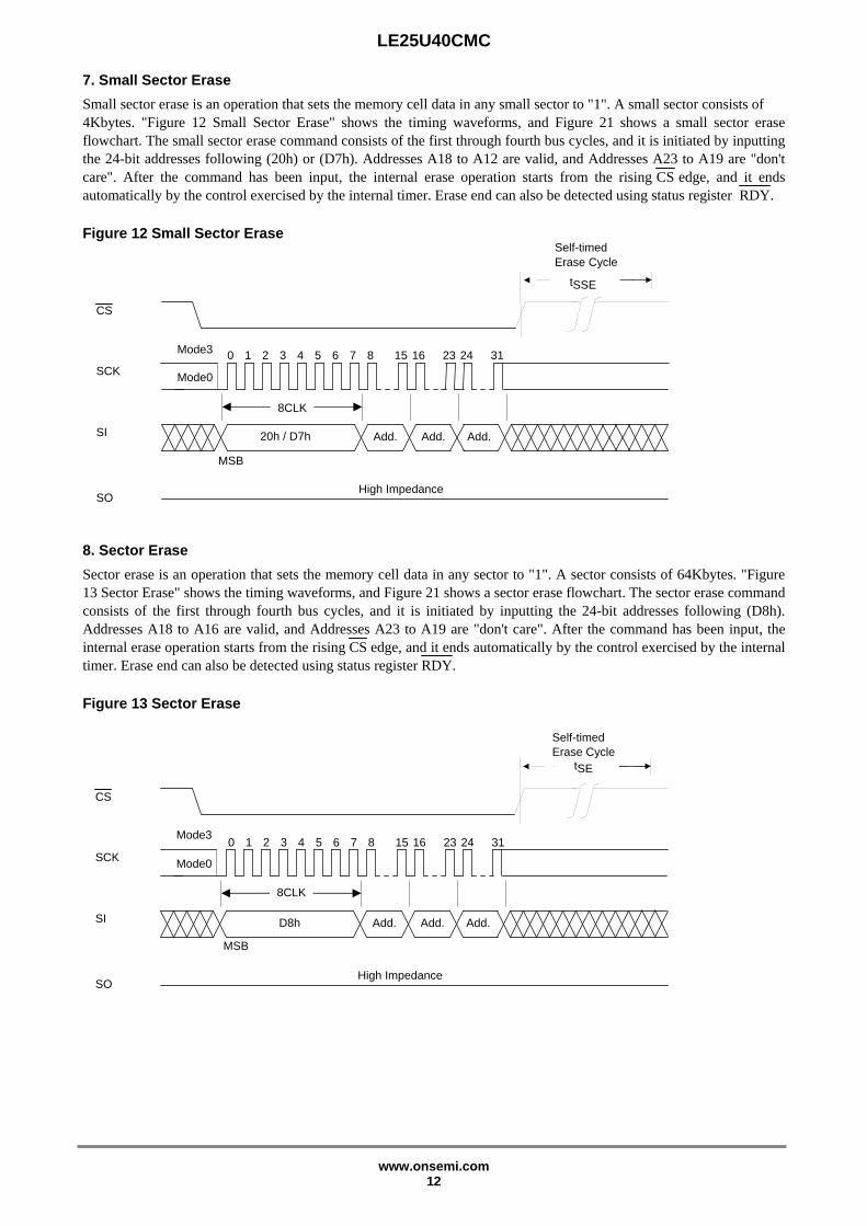
7. Small Sector Erase
Small sector erase is an operation that sets the memory cell data in any small sector to "1". A small sector consists of 4Kbytes. "Figure 12 Small Sector Erase" shows the timing waveforms, and Figure 21 shows a small sector erase flowchart. The small sector erase command consists of the first through fourth bus cycles, and it is initiated by inputting the 24-bit addresses following (20h) or (D7h). Addresses A18 to A12 are valid, and Addresses A23 to A19 are "don't care". After the command has been input, the internal erase operation starts from the rising CS edge, and it ends automatically by the control exercised by the internal timer. Erase end can also be detected using status register RDY. Figure 12 Small Sector Erase
8. Sector Erase
Sector erase is an operation that sets the memory cell data in any sector to "1". A sector consists of 64Kbytes. "Figure 13 Sector Erase" shows the timing waveforms, and Figure 21 shows a sector erase flowchart. The sector erase command consists of the first through fourth bus cycles, and it is initiated by inputting the 24-bit addresses following (D8h). Addresses A18 to A16 are valid, and Addresses A23 to A19 are "don't care". After the command has been input, the internal erase operation starts from the rising CS edge, and it ends automatically by the control exercised by the internal timer. Erase end can also be detected using status register RDY. Figure 13 Sector Erase
Self-timed Erase Cycle
SCK
SI
High Impedance SO
CS
tSSE
Add. 20h / D7h Add. Add.
150 1 2 3 4 5 6 7 8 2316 24 31Mode3
Mode0
8CLK
MSB
SCK
SI
High Impedance SO
CS
tSE
Self-timed Erase Cycle
Add. D8h Add. Add.
150 1 2 3 4 5 6 7 8 2316 24 31Mode3
Mode0
8CLK
MSB

LE25U40CMC
www.onsemi.com 13
9. Chip Erase
Chip erase is an operation that sets the memory cell data in all the sectors to "1". "Figure 14 Chip Erase" shows the timing waveforms, and Figure 21 shows a chip erase flowchart. The chip erase command consists only of the first bus cycle, and it is initiated by inputting (60h) or (C7h). After the command has been input, the internal erase operation starts from the rising CS edge, and it ends automatically by the control exercised by the internal timer. Erase end can also be detected using status register RDY. Figure 14 Chip Erase
10. Page Program
Page program is an operation that programs any number of bytes from 1 to 256 bytes within the same sector page (page addresses: A18 to A8). Before initiating page program, the data on the page concerned must be erased using small sector erase, sector erase, or chip erase. "Figure 15 Page Program" shows the page program timing waveforms, and Figure 22 shows a page program flowchart. After the falling CS, edge, the command (02H) is input followed by the 24-bit addresses. Addresses A18 to A0 are valid. The program data is then loaded at each rising clock edge until the rising CS edge, and data loading is continued until the rising CS edge. If the data loaded has exceeded 256 bytes, the 256 bytes loaded last are programmed. The program data must be loaded in 1-byte increments, and the program operation is not performed at the rising CS edge occurring at any other timing. Figure 15 Page Program
SCK
SI
High Impedance SO
CS
tCHE
Self-timed Erase Cycle
60h / C7h
0 1 2 3 4 5 6 7 Mode3
Mode0
8CLK
MSB
tPP
Self-timed Program Cycle
SCK
SI
High Impedance SO
CS
PD Add. Add. 02h Add. PD
150 1 2 3 4 5 6 7 8 2316 24 31 32 39 40 47Mode3
Mode0
8CLK
PD
2079
MSB

LE25U40CMC
www.onsemi.com 14
11. Silicon ID Read
ID read is an operation that reads the manufacturer code and device ID information. The silicon ID read command is not accepted during writing. There are two methods of reading the silicon ID, each of which is assigned a device ID. In the first method, the read command sequence consists only of the first bus cycle in which (9Fh) is input. In the subsequent bus cycles, the manufacturer code 62h which is assigned by JEDEC, 2-byte device ID code (memory type, memory capacity), and reserved code are output sequentially. The 4-byte code is output repeatedly as long as clock inputs are present, "Table 7-1 JEDEC ID code " lists the silicon ID codes and "Figure 16-a JEDEC ID read" shows the JEDEC ID read timing waveforms. The second method involves inputting the ID read command. This command consists of the first through fourth bus cycles, and the one bite silicon ID can be read when 24 dummy bits are input after (ABh). "Table 7-2 ID code " lists the silicon ID codes and "Figure 16-b ID read" shows the ID read timing waveforms. If the SCK input persists after a device code is read, that device code continues to be output. The data output is transmitted starting at the falling edge of the clock for bit 0 in the fourth bus cycle and the silicon ID read sequence is finished by setting CS high. Table 7-1 JEDEC ID code Table 7-2 ID code
Output code Output Code
Manufacturer code 62h 1 byte device ID
6E
(LE25U40CMC) 2 byte device ID
Memory type 06h
Memory capacity code 13h(4M Bit)
Device code 1 00h
Figure 16-a JEDEC ID Read
Figure 16-b ID Read
CS
High Impedance 13h 06h 62h
SCK
SO
SI 9Fh
15
MSB MSB MSB
0 1 2 3 4 5 6 7 8 2316 24 31 39
8CL
Mode0
Mode3 32
00h
MSB
62h
MSB
CS
High Impedance 6Eh 6Eh
SCK
SO
SI ABh X X
15
MSB MSB
0 1 2 3 4 5 6 7 8 2316 24 31 39
8CL
Mode0
Mode3 32
X

LE25U40CMC
www.onsemi.com 15
12. Hold Function
Using the HOLD pin, the hold function suspends serial communication (it places it in the hold status). "Figure17 HOLD" shows the timing waveforms. The device is placed in the hold status at the falling HOLD edge while the logic level of SCK is low, and it exits from the hold status at the rising HOLD edge. When the logic level of SCK is high, HOLD must not rise or fall. The hold function takes effect when the logic level of CS is low, the hold status is exited and serial communication is reset at the rising CS edge. In the hold status, the SO output is in the high-impedance state, and SI and SCK are "don't care". Figure 17 HOLD
13. Power-on
In order to protect against unintentional writing, CS must be within at VDD-0.3 to VDD+0.3 on power-on. After power-on, the supply voltage has stabilized at VDD min. or higher, waits for tPU before inputting the command to start a device operation. The device is in the standby state and not in the power-down state after power is turned on. To put the device into the power-down state, it is necessary to enter a power-down command. Figure 18 Power-on Timing
CS
HOLD
SCK
SO
Active HOLD Active
tHH
tHS
tHLZ tHHZ
High Impedance
tHH
tHS
VDD(Max)
VDD(Min)
VDD
0V
tPU
CS = VDD level Full Access Allowed

LE25U40CMC
www.onsemi.com 16
14. Hardware Data Protection
LE25U40CMC incorporates a power-on reset function. The following conditions must be met in order to ensure that the power reset circuit will operate stably. No guarantees are given for data in the event of an instantaneous power failure occurring during the writing period.
Figure 19 Power-down Timing
Power-on timing
Parameter Symbol spec
unit min max
power-on to operation time tPU 100 µs
power-down time tPD 10 ms
power-down voltage tBOT 0.2 V
14. Software Data Protection
The LE25U40CMC eliminates the possibility of unintentional operations by not recognizing commands under the following conditions.
When a write command is input and the rising CS edge timing is not in a bus cycle (8 CLK units of SCK) When the page program data is not in 1-byte increments When the status register write command is input for 2 bus cycles or more
15. Decoupling Capacitor
A 0.1F ceramic capacitor must be provided to each device and connected between VDD and VSS in order to ensure that the device will operate stably.
VDD(Max)
VDD(Min)
VDD
0V vBOT
tPD

LE25U40CMC
www.onsemi.com 17
Specifications Absolute Maximum Ratings
Parameter Symbol Conditions Ratings unit
Maximum supply voltage VDD max With respect to VSS 0.5 to +4.6 V
DC voltage (all pins) VIN/VOUT With respect to VSS 0.5 to VDD+0.5 V
Storage temperature Tstg 55 to +150 C
Operating Conditions
Parameter Symbol Conditions Ratings unit
Operating supply voltage VDD 2.3 to 3.6 V
Operating ambient temperature Topr 40 to 85 C
Allowable DC Operating Conditions
Parameter Symbol Conditions Ratings
unit min typ max
Read mode operating current ICCR SCK=0.1VDD/0.9VDD,
HOLD=WP=0.9VDD,
Output = open Single
25MHz 6 mA
40MHz 10
Dual 40MHz 12 mA
Write mode operating current (erase + page program)
ICCW tSSE= tSE= tCHE=typ.,tPP=max 15 mA
CMOS standby current ISB CS=VDD, HOLD=WP=VDD,
SI=VSS/VDD, SO=open, 50 A
Power-down standby current IDSB CS=VDD, HOLD=WP=VDD,
SI=VSS/VDD, SO=open, 10 A
Input leakage current ILI 2 A
Output leakage current ILO 2 A
Input low voltage VIL 0.3 0.3VDD V
Input high voltage VIH 0.7VDD VDD+0.3 V
Output low voltage VOL IOL=100A, VDD=VDD min 0.2 V
IOL=1.6mA, VDD=VDD min 0.4
Output high voltage VOH IOH=100A, VDD=VDD min VDD0.2 V
Data hold, Rewriting frequency
Parameter condition min max unit
Rewriting frequency Program/Erase 100,000 times/ Sector
Status resister write 1,000 times
Data hold 20 year
Pin Capacitance at Ta=25C, f=1MHz
Parameter Symbol Conditions Ratings
unit max
Output pin capacitance CSO VSO=0V 12 pF
Input pin Capacitance CIN VIN=0V 6 pF
Note: These parameter values do not represent the results of measurements undertaken for all devices but rather values for some of the sampled devices.
Stresses exceeding those listed in the Maximum Ratings table may damage the device. If any of these limits are exceeded, device functionality should not be assumed,damage may occur and reliability may be affected.
Functional operation above the stresses listed in the Recommended Operating Ranges is not implied. Extended exposure to stresses beyond the RecommendedOperating Ranges limits may affect device reliability.

LE25U40CMC
www.onsemi.com 18
AC Characteristics
Parameter Symbol Ratings
unit min typ max
Clock frequency Read instruction(03h)
fCLK 25 MHz
All instructions except for read(03h) 40 MHz
Input signal rising/falling time tRF 0.1 V/ns
SCK logic high level pulse width 25MHz
tCLHI 16 ns
40MHz 11.5 ns
SCK logic low level pulse width 25MHz
tCLLO 16 ns
40MHz 11.5 ns
CS setup time tCSS 8 ns
CS hold time tCSH 8 ns
Data setup time tDS 2 ns
Data hold time tDH 5 ns
CS wait pulse width tCPH 25 ns
Output high impedance time from CS tCHZ 8 ns
Output data time from SCK tV 8 11 ns
Output data hold time tHO 1 ns
Output low impedance time from SCK tCLZ 0 ns
HOLD setup time tHS 5 ns
HOLD hold time tHH 3 ns
Output low impedance time from HOLD tHLZ 9 ns
Output high impedance time from HOLD tHHZ 9 ns
WP setup time tWPS 20 ns
WP hold time tWPH 20 ns
Power-down time tDP 3 s
Power-down recovery time tPDR 3 s
Write status register time tSRW 5 15 ms
Page programming cycle time tPP 4 5 ms
Small sector erase cycle time tSSE 40 150 ms
Sector erase cycle time tSE 80 250 ms
Chip erase cycle time tCHE 0.25 2.0 s
AC Test Condtions Input pulse level ··········· 0.2VDD to 0.8VDD Input rising/falling time ·· 5ns Input timing level ········· 0.3VDD, 0.7VDD Output timing level ······· 1/2VDD Output load ················ 30pF Note: As the test conditions for "typ", the measurements are conducted using 2.5v for VDD at room temperature.
0.8VDD
0.2VDD
0.7VDD
1/2VDD
0.3VDD
input level input / output timing level
Product parametric performance is indicated in the Electrical Characteristics for the listed test conditions, unless otherwise noted. Product performance may not beindicated by the Electrical Characteristics if operated under different conditions.

LE25U40CMC
www.onsemi.com 19
Timing waveforms Serial Input Timing
Serial Output Timing
Hold Timing
Status resistor write Timing
High Impedance
tDH
tCPH
tDS
tCSH tCSS
CS
DATA VALID
SO
SI
SCK
High Impedance
tCSS tCSH tCLHI tCLLO
tHO tCHZ tCLZ
SI
tV
CS
SO
SCK
DATA VALID
SI
CS
SCK
HOLD
tHH tHS tHH tHS
tHHZ tHLZ
High Impedance
tWPH tWPS CS
WP

LE25U40CMC
www.onsemi.com 20
Figure 20 Status Register Write Flowchart
Status register write
Start
05h Set status register read command
Set status register write command
status register write start on rising edge of CS
End of status register write
YES
Bit 0= “0” ?
06h Write enable
01h
NO
* Automatically placed in write disabled state at the end of the status register write
Data

LE25U40CMC
www.onsemi.com 21
Figure 21 Erase Flowcharts
Start
05h Set status register read command
Set small sector erase command
Address 1
Address 2
Start erase on rising edge of CS
End of erase
Bit 0 = “0” ?
YES
Small sector erase
Address 3
06h Write enable
20h / D7h
NO
* Automatically placed in write disabled state at the end of the erase
Start
05h Set status register read command
Set sector erase command
Address 1
Address 2
Start erase on rising edge of CS
End of erase
Bit 0 = “0” ?
YES
Sector erase
Address 3
06h Write enable
D8h
NO
* Automatically placed in write disabled state at the end of the erase

LE25U40CMC
www.onsemi.com 22
Figure 22 Page Program Flowchart
Start
05h Set status register read command
Set chip erase command
Start erase on rising edge of CS
End of erase
Bit 0 = “0” ?
YES
Chip erase
06h Write enable
60h / C7h
NO
* Automatically placed in write disabled state at the end of the erase
Page program
Start
05h Set status register read command
Set page program command
Address 1
Address 2
Start program on rising edge of CS
End of programming
YES
Bit 0= “0” ?
Address 3
06h Write enable
02h
NO
* Automatically placed in write disabled state at the end of the programming operation.
Data 0
Data n

LE25U40CMC
www.onsemi.com 23
PART NAME DESCRIPTION for LE25U40C series
LE 25 U 40 C MC XXX - A H - X
Option (For custom usage) In this case, Distinction of Assembly site Environment (Legacy rule) None : Including Pb E : Lead Free H : Lead & Halogen Free
Packing (Legacy rule)
A : Tape Reel Option (For custom usage) None : Standard product
Package type
MC : SOIC8 (SOP8) MD : SOIC8 (SOP8) QE : VSON8 6 x 5 QH : VSON8 4 x 3
Die Generation
None : 1st generation A : 2nd B : 3rd C : 4th
Density
20 : 2M-bit 40 : 4M-bit 80 or 81 : 8M-bit 161 : 16M-bit
Supply voltage
V : 3.0V~3.6V, W : 2.7V~3.6V U : 2.3V~ , S : 1.65V~
Product Family
25 : SPI Serial Flash Memory 26 : Custom specification product

LE25U40CMC
www.onsemi.com 24
ON Semiconductor and the ON logo are registered trademarks of Semiconductor Components Industries, LLC (SCILLC) or its subsidiaries in the United Statesand/or other countries. SCILLC owns the rights to a number of patents, trademarks, copyrights, trade secrets, and other intellectual property. A listing ofSCILLC’s product/patent coverage may be accessed at www.onsemi.com/site/pdf/Patent-Marking.pdf . SCILLC reserves the right to make changes withoutfurther notice to any products herein. SCILLC makes no warranty, representation or guarantee regarding the suitability of its products for any particular purpose,nor does SCILLC assume any liability arising out of the application or use of any product or circuit, and specifically disclaims any and all liability, includingwithout limitation special, consequential or incidental damages. “Typical” parameters which may be provided in SCILLC data sheets and/or specifications canand do vary in different applications and actual performance may vary over time. All operating parameters, including “Typicals” must be validated for eachcustomer application by customer’s technical experts. SCILLC does not convey any license under its patent rights nor the rights of others. SCILLC products arenot designed, intended, or authorized for use as components in systems intended for surgical implant into the body, or other applications intended to support orsustain life, or for any other application in which the failure of the SCILLC product could create a situation where personal injury or death may occur. ShouldBuyer purchase or use SCILLC products for any such unintended or unauthorized application, Buyer shall indemnify and hold SCILLC and its officers,employees, subsidiaries, affiliates, and distributors harmless against all claims, costs, damages, and expenses, and reasonable attorney fees arising out of,directly or indirectly, any claim of personal injury or death associated with such unintended or unauthorized use, even if such claim alleges that SCILLC wasnegligent regarding the design or manufacture of the part. SCILLC is an Equal Opportunity/Affirmative Action Employer. This literature is subject to allapplicable copyright laws and is not for resale in any manner.
Figure 23 Making Diagrams ORDERING INFORMATION
Device Package Shipping (Qty / Packing)
LE25U40CMC-AH SOIC-8 / SOP8J (200mil) (Pb-Free / Halogen Free)
2000 / Tape & Reel
† For information on tape and reel specifications, including part orientation and tape sizes, please refer to our Tape and Reel Packaging Specifications Brochure, BRD8011/D. http://www.onsemi.com/pub_link/Collateral/BRD8011-D.PDF
25FU406C =Specific Device Code 00 =Blank Data (entire memory cell data are FFh) Y =Year M =Month XXX =Serial Number
25FU406C
YMxxx
00