Embed Size (px)
Citation preview
EFFECT OF LEAD-FREE SOLDER AND GOLD CONTENT ON THE SHEAR
STRENGTH, TOUGHNESS, IMC AND VOID FORMATION
By
OO CHENG EE
Thesis submitted in fulfilment of the
requirement for degree
of Master of science
May 2004
ii
ACKNOWLEDGEMENT
Firstly, I would like to thank my project supervisor, Dr. Azizan Aziz and co-supervisor,
Dr. Luay Bakir Hussain for their guidance, advice and help throughout the whole
research project.
Besides that, I would like to thank my site supervisor OP Lim for his full support in
getting the project done.
Not forgetting to thank the school of Material Engineering for allowing me to do
research with the faculty in order my for knowledge and career enhancement. The
many chances given to me to present in front of postgraduates students and gather
inputs and insights from them is highly appreciated.
Besides, I would like to express my sincere thanks to Peter Collins representing
Commercial Department of National Physical Laboratory (NPL), United Kingdom in
granting the permission to use the chart on Gold Embrittlement Prevention Guideline
(Figure 2.4) by NPL in this master report.
Last but not least, thanks to all others directly or indirectly helping up with the project
to make the project a success.
iii
CONTENTS
1.0ACKNOWLEDGEMENT ii
CONTENTS iii
LIST OF FIGURES vii
LIST OF TABLES x
LIST OF ABBREVIATIONS xi
ABSTRACT xii
ABSTRAK xiii
CHAPTER 1: INTRODUCTION
Introduction 1
1 .1 Objectives 4
CHAPTER 2: LITERATURE REVIEW
2.1 Introduction 5
2.2 Lead Free Alternatives 5
2.3 Effect of tin-lead (Pb) to solder system 109
2.4 2.3.1 Adverse Effects of Lead (Pb)
110
2.3.2 Adverse Effects of Tin (Sn) 12
Formatted: Bullets and Numbering
Formatted: Bullets and Numbering
iv
2.52.4 Solder Characteristic 13
Effect of Tin (Sn) to solder system
12
2.6Solder Characteristic 13
2.46.1 Melting Temperature 13
2.46.2 Microstructure 14
2.46.3 Intermetallic Compound (IMC) 14
2.4.6.4 Mechanical Properties 15
2.64.4.1 Time-Independent Monotonic Deformation 16
2.46.4.2 Time Dependent Monotonic Deformation 16
2.46.4.3 Cyclic Deformation or Fatigue 17
2.72.5 Why Gold is used 18
2.82.6 Thick Gold versus Thin Gold
19Gold in Semiconductors and Microelectronics
18
2.9 Thick Gold versus Thin Gold 19
2.102.7 Gold Solder Embrittlement Issue
20
2.112.8 AuSn Intermetallic
23
2.122.9 AnSn Intermetallic Failure Mechanism
25
Formatted: Bullets and Numbering
Formatted: Bullets and Numbering
v
2.132.10 Gold Interaction with Lead Free Solders
26
2.142.11 General Guideline to prevent gold embrittlement
28
2.152.12 Kinkendall Effect
30
2.162.13 Design of Experiment
32
2.163.1 Design Type 34
2.163.2 ANOVA (Analysis of Variance)
35
2.172.14 Shear Test
42
CHAPTER 3: METHODOLOGY
3.1 Introduction 46
3.2 List of equipment 46
3.3 Materials 46
3.4 Experiment Procedure 47
3.4.1 Design of Experiment (DOE) 48 3.4.1.1 Assumption 49
3.4.2 Material Preparation 52
3.4.3 Experiment Processes/Testing/SEM/EDX 53
Formatted: Bullets and Numbering
vi
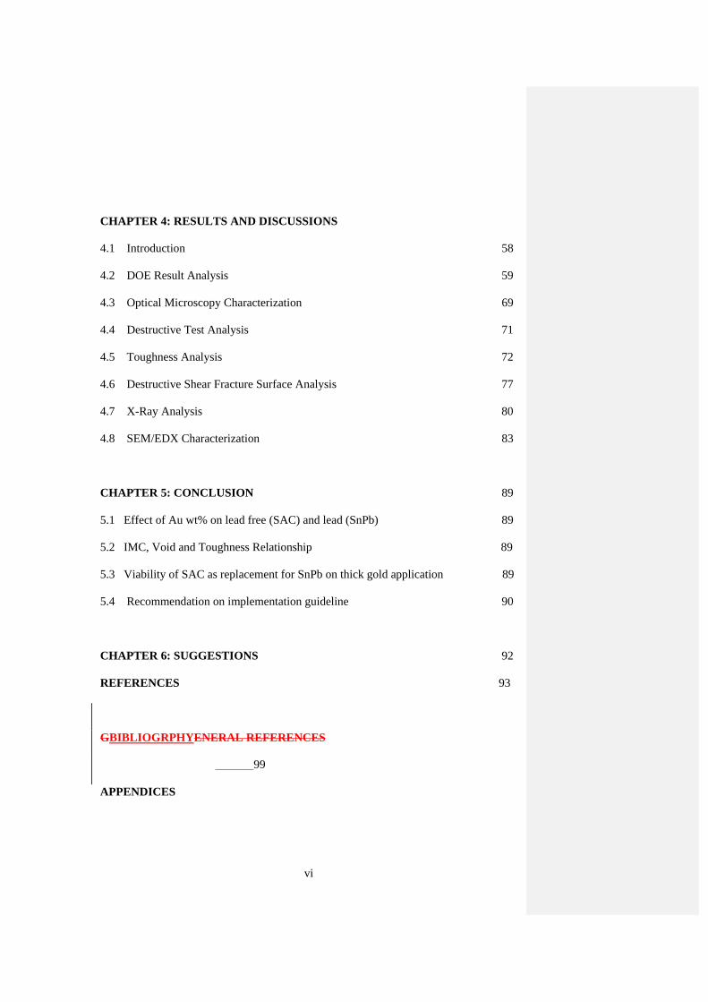
CHAPTER 4: RESULTS AND DISCUSSIONS
4.1 Introduction 58
4.2 DOE Result Analysis 59
4.3 Optical Microscopy Characterization 69
4.4 Destructive Test Analysis 71 4.5 Toughness Analysis 72
4.6 Destructive Shear Fracture Surface Analysis 77
4.7 X-Ray Analysis 80
4.8 SEM/EDX Characterization 83
CHAPTER 5: CONCLUSION 89
5.1 Effect of Au wt% on lead free (SAC) and lead (SnPb) 89
5.2 IMC, Void and Toughness Relationship 89
5.3 Viability of SAC as replacement for SnPb on thick gold application 89
5.4 Recommendation on implementation guideline 90
CHAPTER 6: SUGGESTIONS 92
REFERENCES 93
GBIBLIOGRPHYENERAL REFERENCES
99
APPENDICES
vii
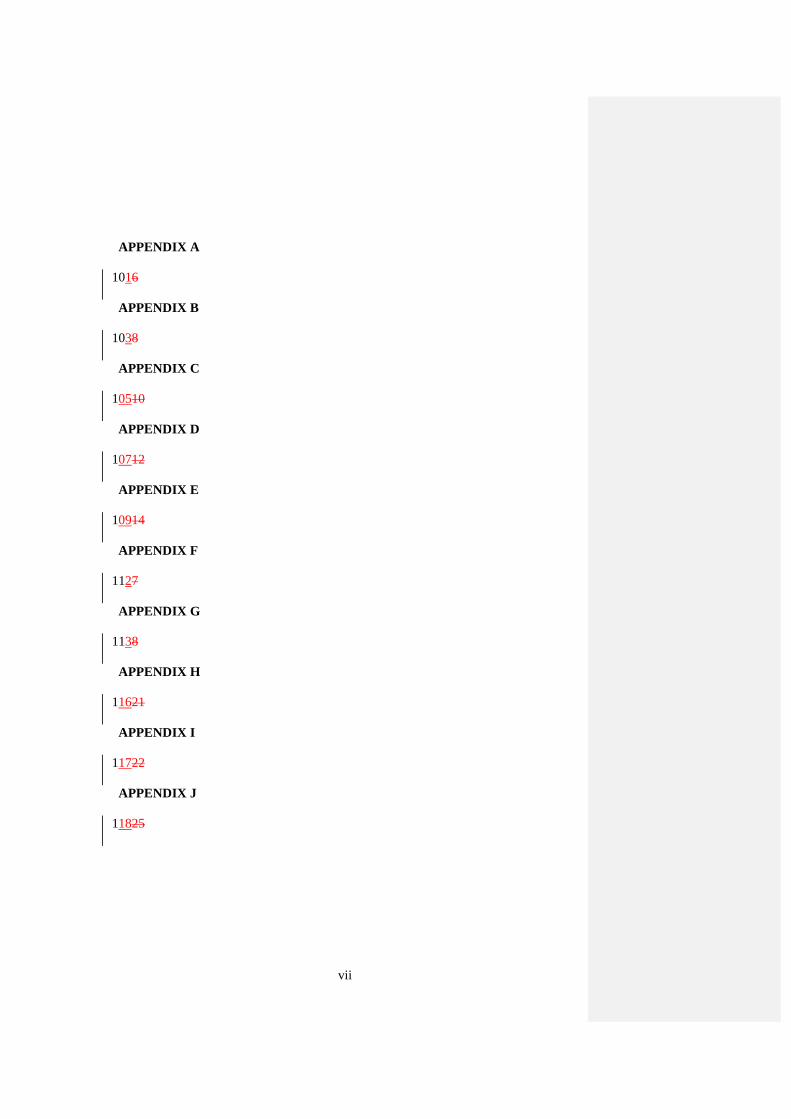
APPENDIX A
1016
APPENDIX B
1038
APPENDIX C
10510
APPENDIX D
10712
APPENDIX E
10914
APPENDIX F
1127
APPENDIX G
1138
APPENDIX H
11621
APPENDIX I
11722
APPENDIX J
11825
viii
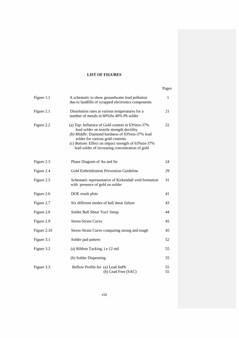
LIST OF FIGURES
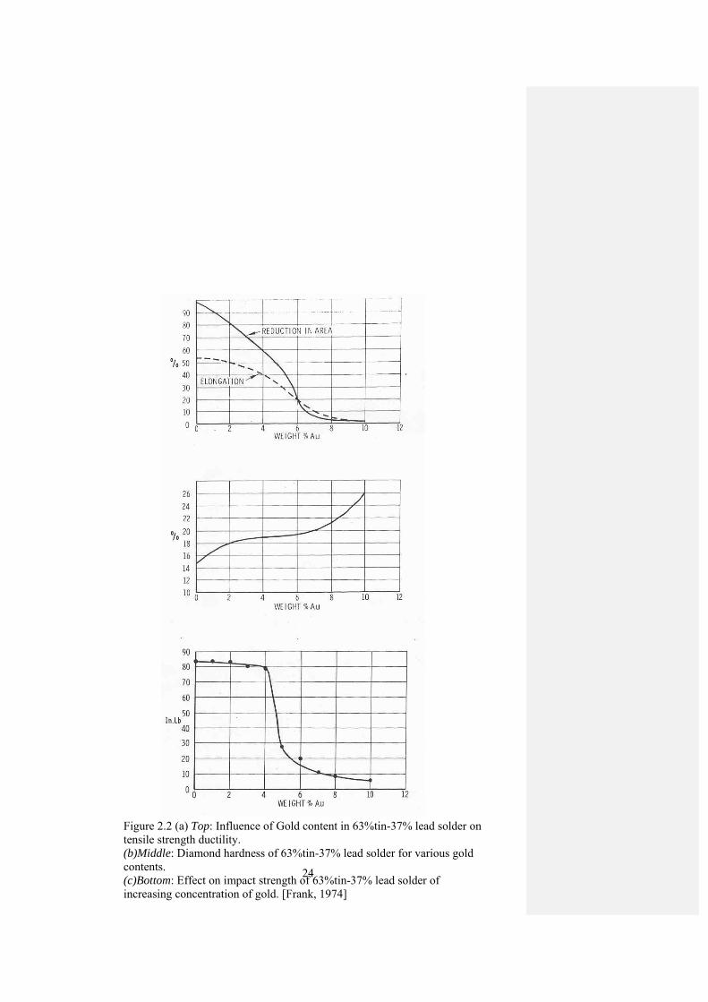
Pages Figure 1.1 A schematic to show groundwater lead pollution 1 due to landfills of scrapped electronics components Figure 2.1 Dissolution rates at various temperatures for a 21 number of metals in 60%Sn 40% Pb solder Figure 2.2 (a) Top: Influence of Gold content in 63%tin-37% 22 lead solder on tensile strength ductility (b) Middle: Diamond hardness of 63%tin-37% lead solder for various gold contents (c) Bottom: Effect on impact strength of 63%tin-37% lead solder of increasing concentration of gold
Figure 2.3 Phase Diagram of Au and Sn 24
Figure 2.4 Gold Embrittlement Prevention Guideline 29
Figure 2.5 Schematic representative of Kirkendall void formation 31 with presence of gold on solder Figure 2.6 DOE result plots 41 Figure 2.7 Six different modes of ball shear failure 43
Figure 2.8 Solder Ball Shear Too1 Setup 44
Figure 2.9 Stress-Strain Curve 45
Figure 2.10 Stress-Strain Curve comparing strong and tough 45
Figure 3.1 Solder pad pattern 52
Figure 3.2 (a) Ribbon Tacking, i.e.12 mil 55
(b) Solder Dispensing 55
Figure 3.3 Reflow Profile for (a) Lead SnPb 55 (b) Lead Free (SAC) 55
ix
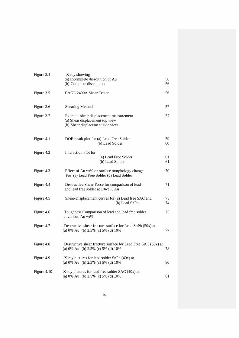
Figure 3.4 X-ray showing (a) Incomplete dissolution of Au 56
(b) Complete dissolution 56 Figure 3.5 DAGE 2400A Shear Tester 56
Figure 3.6 Shearing Method 57 Figure 3.7 Example shear displacement measurement 57 (a) Shear displacement top view
(b) Shear displacement side view Figure 4.1 DOE result plot for (a) Lead Free Solder 59 (b) Lead Solder 60 Figure 4.2 Interaction Plot for (a) Lead Free Solder 61 (b) Lead Solder 61 Figure 4.3 Effect of Au wt% on surface morphology change 70 For (a) Lead Free Solder (b) Lead Solder
Figure 4.4 Destructive Shear Force for comparison of lead 71 and lead free solder at 10wt % Au Figure 4.5 Shear-Displacement curves for (a) Lead free SAC and 73 (b) Lead SnPb 74 Figure 4.6 Toughness Comparison of lead and lead free solder 75 at various Au wt%. Figure 4.7 Destructive shear fracture surface for Lead SnPb (50x) at (a) 0% Au (b) 2.5% (c) 5% (d) 10% 77
Figure 4.8 Destructive shear fracture surface for Lead Free SAC (50x) at (a) 0% Au (b) 2.5% (c) 5% (d) 10% 78 Figure 4.9 X-ray pictures for lead solder SnPb (40x) at (a) 0% Au (b) 2.5% (c) 5% (d) 10% 80 Figure 4.10 X-ray pictures for lead free solder SAC (40x) at (a) 0% Au (b) 2.5% (c) 5% (d) 10% 81
x
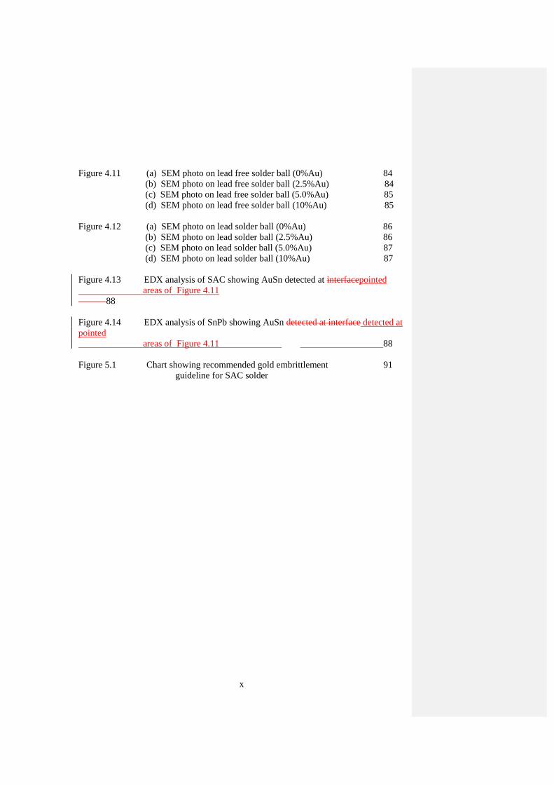
Figure 4.11 (a) SEM photo on lead free solder ball (0%Au) 84 (b) SEM photo on lead free solder ball (2.5%Au) 84 (c) SEM photo on lead free solder ball (5.0%Au) 85 (d) SEM photo on lead free solder ball (10%Au) 85 Figure 4.12 (a) SEM photo on lead solder ball (0%Au) 86 (b) SEM photo on lead solder ball (2.5%Au) 86 (c) SEM photo on lead solder ball (5.0%Au) 87 (d) SEM photo on lead solder ball (10%Au) 87 Figure 4.13 EDX analysis of SAC showing AuSn detected at interfacepointed areas of Figure 4.11 88 Figure 4.14 EDX analysis of SnPb showing AuSn detected at interface detected at pointed areas of Figure 4.11 88 Figure 5.1 Chart showing recommended gold embrittlement 91 guideline for SAC solder
xi
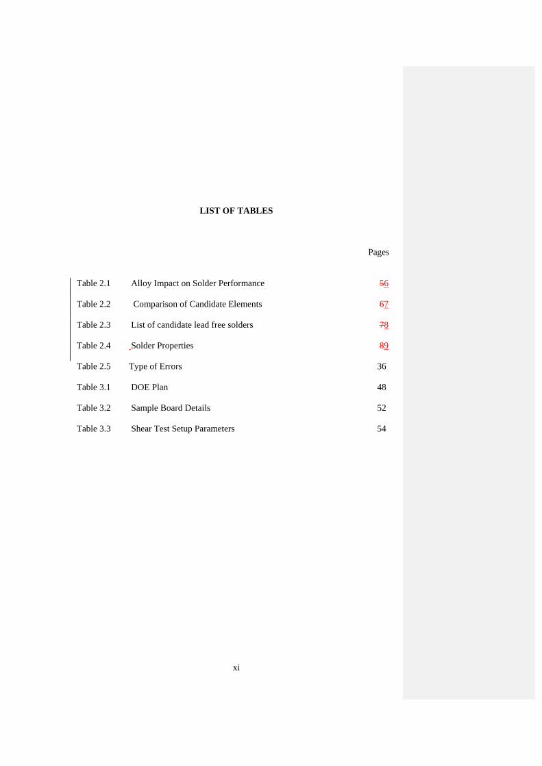
LIST OF TABLES
Pages
Table 2.1 Alloy Impact on Solder Performance 56
Table 2.2 Comparison of Candidate Elements 67
Table 2.3 List of candidate lead free solders 78
Table 2.4 Solder Properties 89
Table 2.5 Type of Errors 36
Table 3.1 DOE Plan 48
Table 3.2 Sample Board Details 52
Table 3.3 Shear Test Setup Parameters 54
xii
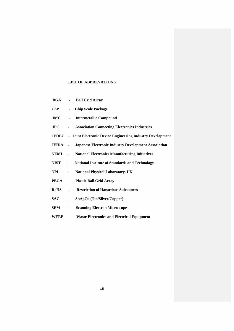
LIST OF ABBREVATIONS
BGA - Ball Grid Array
CSP - Chip Scale Package
IMC - Intermetallic Compound
IPC - Association Connecting Electronics Industries
JEDEC - Joint Electronic Device Engineering Industry Development
JEIDA - Japanese Electronic Industry Development Association NEMI - National Electronics Manufacturing Initiatives
NIST - National Institute of Standards and Technology NPL - National Physical Laboratory, UK PBGA - Plastic Ball Grid Array RoHS - Restriction of Hazardous Substances
SAC - SnAgCu (Tin/Silver/Copper)
SEM - Scanning Electron Microscope
WEEE - Waste Electronics and Electrical Equipment
xiii
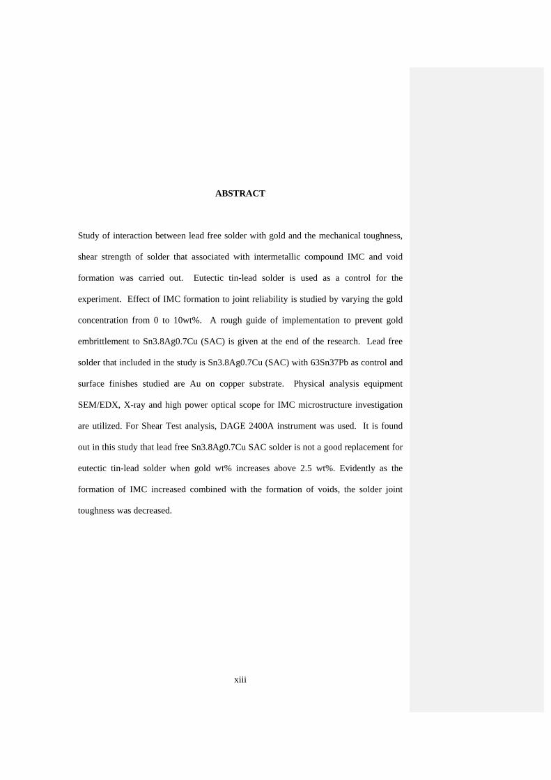
ABSTRACT
Study of interaction between lead free solder with gold and the mechanical toughness,
shear strength of solder that associated with intermetallic compound IMC and void
formation was carried out. Eutectic tin-lead solder is used as a control for the
experiment. Effect of IMC formation to joint reliability is studied by varying the gold
concentration from 0 to 10wt%. A rough guide of implementation to prevent gold
embrittlement to Sn3.8Ag0.7Cu (SAC) is given at the end of the research. Lead free
solder that included in the study is Sn3.8Ag0.7Cu (SAC) with 63Sn37Pb as control and
surface finishes studied are Au on copper substrate. Physical analysis equipment
SEM/EDX, X-ray and high power optical scope for IMC microstructure investigation
are utilized. For Shear Test analysis, DAGE 2400A instrument was used. It is found
out in this study that lead free Sn3.8Ag0.7Cu SAC solder is not a good replacement for
eutectic tin-lead solder when gold wt% increases above 2.5 wt%. Evidently as the
formation of IMC increased combined with the formation of voids, the solder joint
toughness was decreased.
xiv
KESAN LOGAM PATERI TANPA PLUMBUM DAN KANDUNGAN EMAS KE
ATAS KEKUATAN RICIH PATERI, KELIATAN, PEMBENTUKAN
KOMPAUN ANTARALOGAM DAN LOMPONG
ABSTRAK
Kajian tentang interaksi antara logam pateri tanpa plumbum dengan emas dan keliatan,
kekuatan ricih yang berkait rapat dengan pembentukan kompaun antaralogam dan
lompong. Eutetik tin-plumblum pateri digunakan sebagai kawalan dalam eksperimen
ini. Kesan pembentukan antaralogam terhadap reliabilitas (kebolehpercayaan) ikatan
pateri dikaji dengan mengubah kepekatan kandungan emas dari 0% hingga 10 %. Satu
panduan tentang aplikasi bagi mengelakkan kesan kerapuhan diberi pada akhir kajian.
Logam pateri tanpa plumbum yang dikaji ialah Tin/3.8Perak/0.7Kuprum (SAC) dan
63Tin37Plumblum sebagai kawalan dan permukaan yang dikaji ialah emas atas
kuprum. Alatan analisis fizik yang digunakan termasuk SEM/EDX, sinar-X, mikroskop
optik berkuasa tinggi untuk kajian mikrostruktur antaralogam dan DAGE 2400A untuk
penguji ricih. Kajian ini mendapati bahawa SAC bukan pengganti yang baik untuk
eutetik tin-plumbum pateri apabila kandungan emas mencapai 2.5%. Selain itu,
terdapat bukti yang jelas bahawa keliatan merosot dengan pertambahan pembentukan
antaralogam dan lompong.
1
CHAPTER 1
INTRODUCTION
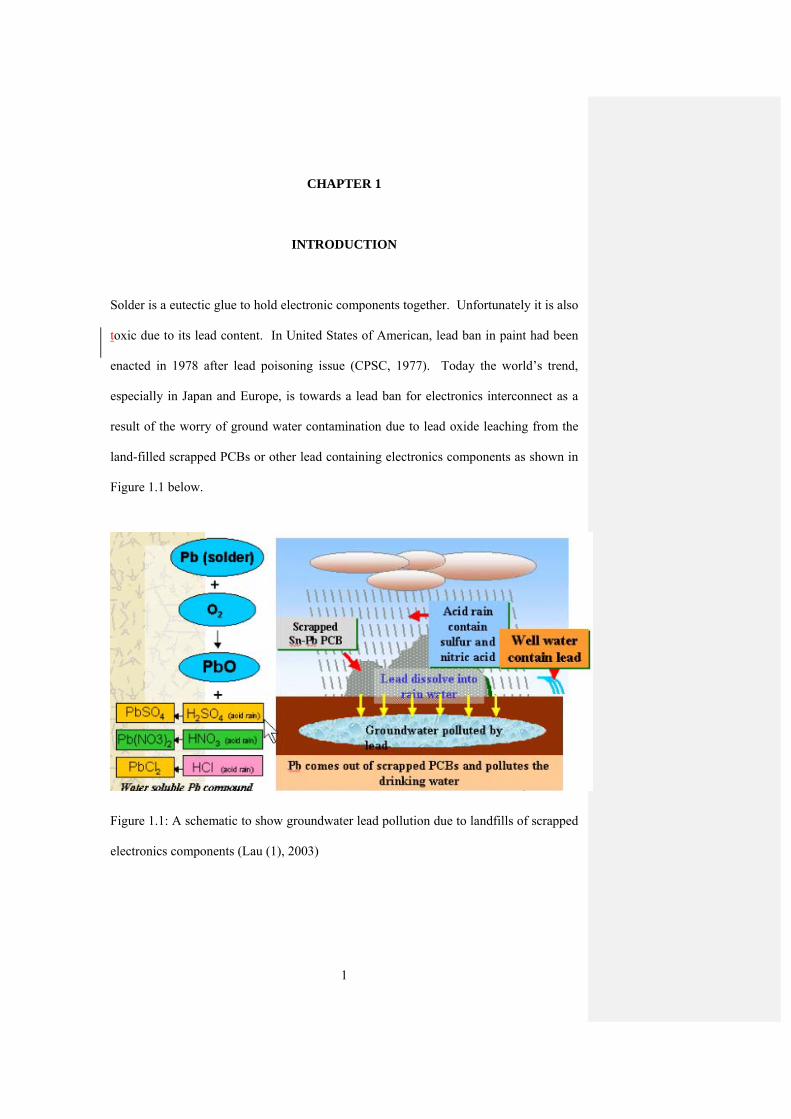
Solder is a eutectic glue to hold electronic components together. Unfortunately it is also
toxic due to its lead content. In United States of American, lead ban in paint had been
enacted in 1978 after lead poisoning issue (CPSC, 1977). Today the world’s trend,
especially in Japan and Europe, is towards a lead ban for electronics interconnect as a
result of the worry of ground water contamination due to lead oxide leaching from the
land-filled scrapped PCBs or other lead containing electronics components as shown in
Figure 1.1 below.
Figure 1.1: A schematic to show groundwater lead pollution due to landfills of scrapped
electronics components (Lau (1), 2003)
2
Lead is known to have adverse health effects when it accumulates in the body over time.
Lead binds strongly to proteins in the body and inhibits normal processing and
functions. Nervous and reproductive system disorders, delays in neurological and
physical development, cognitive and behavioral changes, as well as reduced production
of hemoglobin resulting in anemia and hypertension are some of the adverse effects of
lead on human health. When the level of lead in the blood exceeds 40ug/100g of blood,
lead poisoning is considered to have occurred (Ng, 2002). A lead level even well below
the established official threshold can be hazardous to a child's neurological and physical
development.
The concern about the use of lead in the electronics industry stems from occupational
exposure, lead waste derived from the manufacturing process and the disposal of
electronics assemblies. Therefore, US Environmental Protection Agency (EPA) has
cited lead and its compounds as one of the top 17 chemicals that pose the greatest threat
to human life and the environment (Mulugeta and Guna, 1998)
This has forced the NEMI (National Electronics Manufacturing Initiatives) taskforce to
work hard towards meeting the ban of lead in electronics application by 1st July, 2006 as
approved by Europe RoHS (Restriction of Hazardous Substances). Their primary
emphasis is on Sn/Ag/Cu (SAC) as “one single solution” for lead replacement (Galen,
2003).
However, some people argue that less than 2% of the production of lead worldwide
(John, 2003) is used in solders for the electronic industry. Therefore the worry about
3
amount of lead from printed circuit board go into landfill may leach into ground water
and endanger marine life is unconvincing for the need of lead ban.
The lead-free debate is no longer about the environmental impact or about technical
issues. It is more to a marketing issue following the success story of Panasonic Japan in
securing an estimated of 11% of market share available after the introduction of lead-
free portable mini-disc player (MiniDisc MJ30) as a green product in October 1998
(John, 2003).
Despite the argument, tThe fact is that the decision of Japanese companies to go lead-
free is forcing the US and Europe to take decision now. Big US companies are
following the main stream now example Intel, the chip giant recently announced its
move to remove all but five per cent of the lead it currently uses to construct processors
and chipsets (Tony, 2004).
The lead-free debate is no longer about the environmental impact or about technical
issues. In the meantime, it is more to a MARKETING issue following the success story
of Panasonic Japan share increment from 4.7% to 15% after the introduction of lead-
free portable mini-disc player (MiniDisc MJ30) as a green product in October 1998.
Besides, Toshiba has developed lead-free solders suitable for high-density cellular
phones. Nortel Networks has produced lead-free Meridian phones at four different sites
in North America and Europe [1].
In short, manufacturers who jump on the lead-free bandwagon now will have the market
advantage—the sooner the better.
4
This had forced the NEMI (National Electronics Manufacturing Initiatives) taskforce to
work hard towards meeting the ban of lead in electronics application by 1st July, 2006 as
approved by Europe RoHS (Restriction of Hazardous Substances). Their primary
emphasis is on Sn/Ag/Cu (SAC) as “one single solution” for lead replacement (Galen,
2003).
However, there are technological issues need to be addressed following the conversion,
mainly about the higher melting point of the lead free solder, tighter process window,
potential damage to heat sensitive components, surface finish incompatibility and the
long-exist gold (Au) embrittlement issue that is concerned to be exaggerated by new
lead free solder SAC especially for thick gold coating (3-5 μm) application in some
industries e.g. microwave and radio frequency industries. However, there are still
lacking in literatures about the interaction of lead free solder e.g. SAC with gold,
especially thick gold. It is interesting to study if the long known gold embrittlement
issue with existing eutectic tin-lead solder will exist for SAC lead free solder as well
and to what extend. The research in this area is important as a fundamental knowledge
for future implementation.
1.1 Objectives
The objectives of the project being run are as follows:
i) To study the effect of Au wt% on lead free (SAC) and lead (SnPb) solder
joint characteristic in terms of shear strength, toughness, IMC and void
formation
5
ii) To study the correlation between IMC with void formation and associated
toughness
iii) To assess the viability of lead free solder (SAC) as a replacement for
existing eutetic lead solder on thick gold application
iv) To establish guideline to avoid gold embrittlement of SAC solder
CHAPTER 2
LITERATURE REVIEW
2.1 Introduction
Solder has long been a popular conductive glue to hold electronic components together
especially eutectic 63Sn37Pb solder. Unfortunately it is also known for its toxicity due
to its lead content. Today, the world’s trend, especially especially in Japanese and
6
Europe, is moving towards a lead ban for electronics interconnect as a result of the
worry of ground water lead contamination due to lead oxide leaching and also
occupational lead health and safety concern. This together with economic pressure has
driven the development works in recent decades to work out the lead free solder
replacement.
2.2 Lead Free Alternatives
Lead free by definition is the electronic products which none of their components or raw
materials contains Lead (Pb) that is intentionally added, or contain more that 0.1% of
incidental Pb impurities by weight. Today there is still no common world standard for
stipulation of lead content as impurities to lead free solders, however JEIDA defined it
as 0.1 weight % while JEDEC defined it as 0.2 weight % (Lau (1), 2003). There are list
of lead free solders available in the markets however for the most economical and
technological means, SAC is always recommended.
Table 2.1 and 2.2 below show some candidates elements for selection in regards to its
impact to solder property, relative cost, toxicity and resource availability. In lieu of
SnPb eutectic, all viable lead-free solder cannot run away from being Sn-based system
(i.e., a minimum of 60 weight % of tin). This was concluded based on fundamental
materials science and practical perspectives (Hwang, 2001). Fundamentals include
metallurgical bonding capability on commonly used substrates, wetting ability during
reflow process, and metallurgical interactions or alloying phenomena between elements.
Practical factors include the availability of natural resources, manufacturability, toxicity
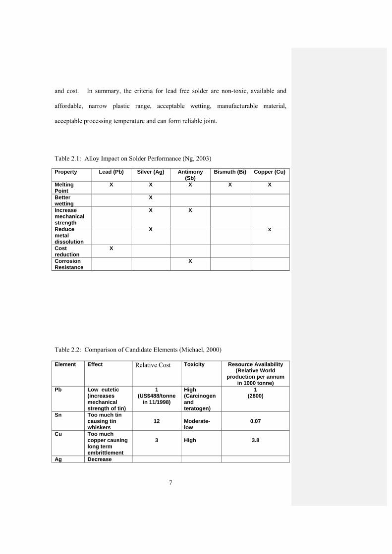
7
and cost. In summary, the criteria for lead free solder are non-toxic, available and
affordable, narrow plastic range, acceptable wetting, manufacturable material,
acceptable processing temperature and can form reliable joint.
Table 2.1: Alloy Impact on Solder Performance (Ng, 2003) Property Lead (Pb) Silver (Ag) Antimony
(Sb) Bismuth (Bi) Copper (Cu)
Melting Point
X X X X X
Better wetting
X
Increase mechanical strength
X X
Reduce metal dissolution
X x
Cost reduction
X
Corrosion Resistance
X
Table 2.2: Comparison of Candidate Elements (Michael, 2000) Element Effect Relative Cost Toxicity Resource Availability
(Relative World production per annum
in 1000 tonne)Pb Low eutetic
(increases mechanical strength of tin)
1 (US$488/tonne
in 11/1998)
High (Carcinogen and teratogen)
1(2800)
Sn Too much tin causing tin whiskers
12 Moderate-
low 0.07
Cu Too much copper causing long term embrittlement
3
High 3.8
Ag Decrease
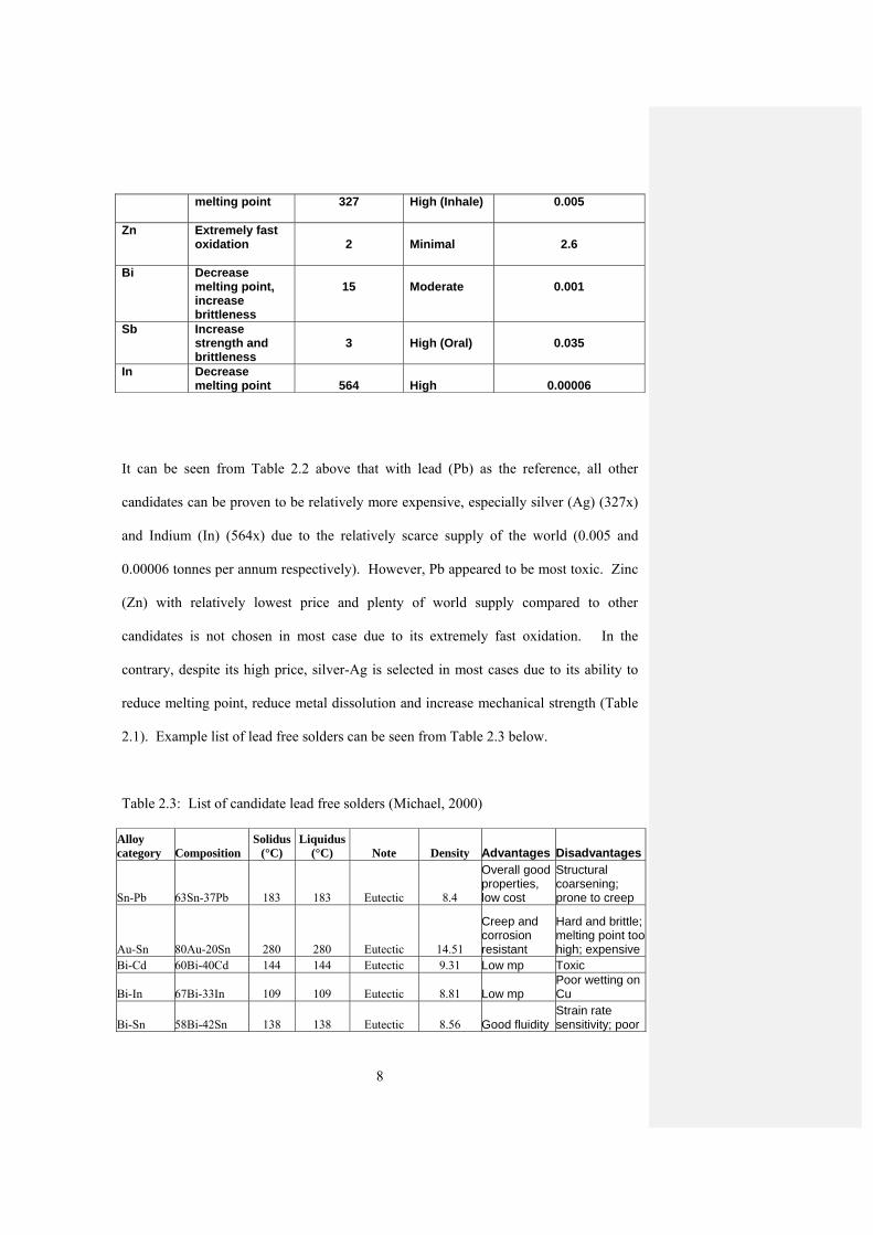
8
melting point
327
High (Inhale) 0.005
Zn Extremely fast oxidation
2
Minimal 2.6
Bi Decrease melting point, increase brittleness
15
Moderate 0.001
Sb Increase strength and brittleness
3
High (Oral)
0.035
In Decrease melting point
564
High
0.00006
It can be seen from Table 2.2 above that with lead (Pb) as the reference, all other
candidates can be proven to be relatively more expensive, especially silver (Ag) (327x)
and Indium (In) (564x) due to the relatively scarce supply of the world (0.005 and
0.00006 tonnes per annum respectively). However, Pb appeared to be most toxic. Zinc
(Zn) with relatively lowest price and plenty of world supply compared to other
candidates is not chosen in most case due to its extremely fast oxidation. In the
contrary, despite its high price, silver-Ag is selected in most cases due to its ability to
reduce melting point, reduce metal dissolution and increase mechanical strength (Table
2.1). Example list of lead free solders can be seen from Table 2.3 below.
Table 2.3: List of candidate lead free solders (Michael, 2000)
Alloy category Composition
Solidus (°C)
Liquidus (°C) Note Density Advantages Disadvantages
Sn-Pb 63Sn-37Pb 183 183 Eutectic 8.4
Overall good properties, low cost
Structural coarsening; prone to creep
Au-Sn 80Au-20Sn 280 280 Eutectic 14.51
Creep and corrosion resistant
Hard and brittle; melting point too high; expensive
Bi-Cd 60Bi-40Cd 144 144 Eutectic 9.31 Low mp Toxic
Bi-In 67Bi-33In 109 109 Eutectic 8.81 Low mp Poor wetting on Cu
Bi-Sn 58Bi-42Sn 138 138 Eutectic 8.56 Good fluidity Strain rate sensitivity; poor
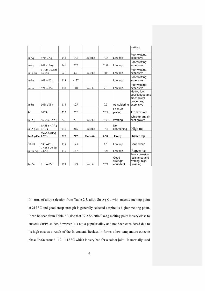
9
wetting
In-Ag 97In-3Ag 143 143 Eutectic 7.38 Low mp Poor wetting; expensive
In-Ag 90In-10Ag 141 237 7.54 Low mp Poor wetting; expensive
In-Bi-Sn 51.0In-32.5Bi-16.5Sn 60 60 Eutectic 7.88 Low mp
Poor wetting; expensive
In-Sn 60In-40Sn 118 ~127 Low mp Poor wetting; expensive
In-Sn 52In-48Sn 118 118 Eutectic 7.3 Low mp Poor wetting; expensive
In-Sn 50In-50Sn 118 125 7.3 Au soldering
Mp too low; poor fatigue and mechanical properties; expensive
Sn 100Sn 232 232 7.28 Ease of plating Tin whisker
Sn-Ag 96.5Sn-3.5Ag 221 221 Eutectic 7.36 Wetting Whisker and tin pest growth
Sn-Ag-Cu 93.6Sn-4.7Ag-1.7Cu 216 216 Eutectic 7.5
No coarsening High mp
Sn-Ag-Cu 96.5Sn3.8Ag 0.7Cu 217 217 Eutectic 7.50 Creep Higher mp
Sn-In 58Sn-42In 118 145 7.3 Low mp Poor creep
Sn-In-Ag 77.2Sn-20.0In-2.8Ag 175 187 7.25 Low mp Expensive
Sn-Zn 91Sn-9Zn 199 199 Eutectic 7.27
Good strength; abundant
Poor corrosion resistance and wetting; high drossing
In terms of alloy selection from Table 2.3, alloy Sn-Ag-Cu with eutectic melting point
at 217 °C and good creep strength is generally selected despite its higher melting point.
It can be seen from Table 2.3 also that 77.2 Sn/20In/2.8Ag melting point is very close to
eutectic Sn/Pb solder, however it is not a popular alloy and not been considered due to
its high cost as a result of the In content. Besides, it forms a low temperature eutectic
phase In/Sn around 112 – 118 °C which is very bad for a solder joint. It normally used
10
if thermo-cycling or end use requirements do not exceed 100 °C. Other lead free solder
candidates like AuSn is normally used for high temperature application which melting
point is high at 280 °C and this solder is expensive due to gold-Au content (80%).
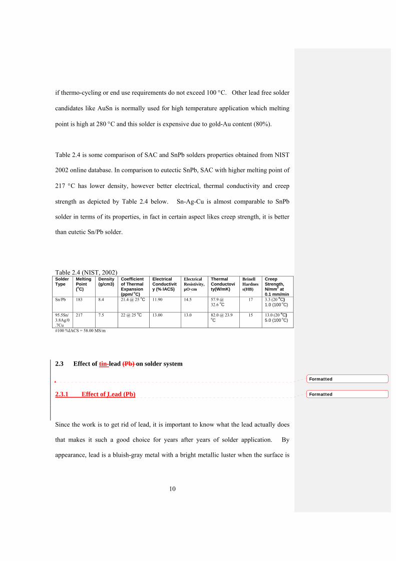
Table 2.4 is some comparison of SAC and SnPb solders properties obtained from NIST
2002 online database. In comparison to eutectic SnPb, SAC with higher melting point of
217 °C has lower density, however better electrical, thermal conductivity and creep
strength as depicted by Table 2.4 below. Sn-Ag-Cu is almost comparable to SnPb
solder in terms of its properties, in fact in certain aspect likes creep strength, it is better
than eutetic Sn/Pb solder.
Table 2.4 (NIST, 2002) Solder Type
Melting Point (oC)
Density(g/cm3)
Coefficient of Thermal Expansion (ppm/ oC)
Electrical Conductivity (% IACS)
Electrical Resistivity, µO·cm
Thermal Conductovity(W/mK)
Brinell Hardness(HB)
Creep Strength, N/mm2 at 0.1 mm/min
Sn/Pb 183 8.4 21.4 @ 25 oC 11.90 14.5 57.9 @ 32.6 oC
17 3.3 (20 oC) 1.0 (100 oC)
95.5Sn/3.8Ag/0.7Cu
217 7.5 22 @ 25 oC 13.00 13.0 82.0 @ 23.9 oC
15 13.0 (20 oC) 5.0 (100 oC)
#100 %IACS = 58.00 MS/m
2.3 Effect of tin-lead (Pb) on solder system
2.3.1 Effect of Lead (Pb)
Since the work is to get rid of lead, it is important to know what the lead actually does
that makes it such a good choice for years after years of solder application. By
appearance, lead is a bluish-gray metal with a bright metallic luster when the surface is
Formatted
Formatted
11
freshly exposed. In ordinary air, the surface deteriorates rapidly, taking on the dull gray
appearance. This tarnish is very tenacious and protects the metallic surface from further
environmental attack, which is why lead were preserved for thousand so years in the
ground or other relative corrosive environment. Lead is very soft metal with great
ductility and can be easily formed. It can form eutectic alloy with tin with melting point
at 183 °C, low enough for most industries application.
As one of the primary components of eutectic solders, lead imparts many technical
advantages to tin-lead solders (Mulugeta and Guna, 1998), including the following:
It reduces the surface tension of pure tin and the lower surface tension of solder
which facilitates wetting (Vianco, 1993)
As an impurity in tin at levels as low as 0.1%, lead prevents the transformation
of white or beta tin to gray or alpha tin upon cooling (see more explanation for
such transformation in section 2.5). The reaction results in a 26% increase in
volume, and the transformation causes loss of structural integrity to the tin.
(Vianco, 1993)
Pb serves as a solvent metal to enable other joint constituents, such as Sn and
Cu, to rapidly form intermetallic bonds.
These factors, combined with lead being a readily available and low cost metal, make it
an ideal alloying element with tin.
However, despite the advantages, it’s also well substantiated that the common thermal
fatigue failure for solder interconnects is linked with the Pb-rich phase. Because of
12
limited solubility and precipitation, Sn solute atoms cannot effectively strengthen the
Pb-rich phase. At room temperature, the limited solubility of Pb in Sn matrix renders it
incapable of improving the plastic deformation slip. Under temperature cycling
(thermomechanical fatigue) condition, this Pb-rich phase tends to coarsen and
eventually, lead to a solder joint crack (Hwang, 2001). It’s therefore hopeful that the
new lead free solder alternative developed with absence of Pb can impart an improved
mechanical behavior.
Meanwhile, it is likely that industry may be increasingly required to recycle lead. The
use of recycled lead for electronics applications, however, can be severely limited since
recycled lead emits alpha particles, which can have detrimental effects on the
performance of integrated circuits (Mulugeta and Guna, 1998).
Today, the world is still lacking comprehensive data about the lead free solder
compared to lead system. The lead based systems have relatively well-established
knowledge base about their physical metallurgy, mechanical properties, flux
chemistries, manufacturing processes and reliability of eutectic tin-lead solders.
Soldering on lead free solder is still a risk and need special attention (Mulugeta and
Guna, 1998).
2.3.2 Effect of Tin (Sn)
2.4 Adverse Effects of Lead
2.5
Formatted
Formatted: Bullets and Numbering
Formatted
Formatted
13
2.6 When lead accumulates in the body over time, it can have adverse health
effects. Lead binds strongly to proteins in the body and inhibits normal
processing and functions. Nervous and reproductive system disorders, delays in
neurological and physical development, cognitive and behavioral changes, as
well as reduced production of hemoglobin resulting in anemia and
hypertension are some of the adverse effects of lead on human health.
2.7
2.8 When the level of lead in the blood exceeds 40ug/100g of blood, lead poisoning
is considered to have occurred (Ng, 2002). A lead level even well below the
established official threshold can be hazardous to a child's neurological and
physical development.
2.9
2.10 The concern about the use of lead in the electronics industry stems from
occupational exposure, lead waste derived from the manufacturing process and
the disposal of electronics assemblies.
2.11
2.12 Therefore, US Environmental Protection Agency (EPA) has cited lead and
its compounds as one of the top 17 chemicals that pose the greatest threat to
human life and the environment (Mulugeta and Guna, 1998)
2.13
2.14
2.15
2.16
2.17
2.18 Effect of Tin (Sn) on solder system Formatted: Bullets and Numbering
14
Because of its ability to wet and spread on a wide range of substrates using mild fluxes,
tin has become the principal component of most solder alloys used for electronic
applications. Tin exists in two different forms with two different crystal structures.
White or β tin has a body centered tetragonal crystal structure and is stable at room
temperature. Gray tin or α tin, which has a diamond cubic crystal structure, is
thermodynamically stable below 13°C. The transformation of β to α tine, also called
"tin pest," takes place when the temperature falls below 13°C, and results in a large
increase in volume that can induce cracking in the tin structure. Consequently, tin pest
can be a problem for applications that operate at temperature below 13°C.
Tin is also prone to whisker growth. Whiskers can be defined as a spontaneous
columnar or cylindrical filament, which rarely branches, of mono-crystalline tin
emanating from the surface of a plating finish. (Irina, 2003). Tin whiskers are
tetragonal β-tin that may grow in response to internal stress in the material or external
loads (Lau (2), 2003). Rapid whisker growth in tin occurs at about 51°C and is
influenced by plating conditions and substrate property. Whiskers do not affect
solderability nor do they cause deterioration of the tin coatings. However, longer
whiskers may cause electrical shorts in PC board assemblies. Elements such as lead
suppress whisker growth in tin, and virtually no whisker growth is encountered in
eutectic tin-lead solder (Mulugeta & Guna, 1998).
15
2.192.4 Solder Characteristic
Soldering is a well-known metallurgical joining method using a filler metal (the solder)
with a melting point below 425°C. In order to form a proper metallurgical bond
between two metals, wetting must takes place. This means that a specific interaction
must take place between liquid solder and the solid surface of the parts to be soldered.
Solders can be classified as soft (melting point below 190 °C) and hard solders (melting
point between 190 to 425 °C). The performance characteristics that are important
include the melting temperature, the microstructure, IMC (intermetallic) formation and
its inherent mechanical strength e.g. shear strength, fatigue behavior and creep behavior.
2.46.1 Melting Temperature
One of the fundamental performance characteristics of solder for industrial applications
is melting temperature. For these applications, the melting temperature of the solder
determines the maximum allowable temperature a product can be exposed to in service
and the maximum processing temperature that devices and substrates can withstand
during soldering. And, it is always desirable to have one same solidus and liquidus
point that is called eutectic point. This eutetic point is desired in order to minimize the
plastic region that is sensitive to mechanical movement or vibration that can lead to
rejectable solder joint. The solidus and liquidus temperatures of various lead-free
solders including Sn-Ag-Cu can be found in Table 2.3. Note that there are binary,
ternaries and quaternaries alloys available.
Formatted: Bullets and Numbering
16
2.46.2 Microstructure
The useful properties of materials are strongly dependent on their microstructure, which
describes the grain structure and the combination of phases present in a material, as well
as its defects, morphology and distribution. Generally, for a material of a given
chemical composition, the microstructure is not constant and varies greatly, depending
on processing and service conditions. In soldering assembly, the time-and-temperature-
dependent soldering profile affects the microstructure of the solder joints, including the
intermetallic layer thickness and the number of intermetallic phases present in the solder
joint. The microstructure variation can drastically affect the fatigue life of the solder
joint. Because operating temperature is a high homologous temperature for solder, the
initial eutectic microstructure evolves over time. Homologous temperature is the ratio
of operating temperature to melting temperature, e.g. 0.5 (= 90°C/ 183°C). The lesser
homologous temperature the better (Mulugeta and Guna, 1998).
2.6.32.4.3 Intermetallic Compounds (IMC)
Intermetallic compound (IMC) is defined as a distinguishable homogeneous phase
having a relatively narrow range of compositions with simple stoichiometric proportion
(Manko, 1979). The intermetallic compounds that are formed at the solder substrate
interface continue to grow over time and increases with rising temperatures. This
growth is a result of a solid-state reaction driven by an energy differential. The solder
substrate reaction is exothermic, which means that the intermetallic compounds that are
formed have a lower energy content than the reacting metal. Example IMC’s are
AuSn4, Cu6Sn5, Cu3Sn, Ni3Sn4 and etc.
Formatted: Bullets and Numbering
17
Each solder joint forms an intermetallic layer with each of the surfaces being joined
together with the malleable tin-lead solder in between. The malleable nature of the tin-
lead solder absorbs some thermal shock and mechanical stress, like a rubber bumper.
This is ideal for the durable solder joint. But solder joints age. The intermetallic
compound grows through time and with temperature. They often work together, but
they can work independently. As time goes by, the intermetallic compound grows.
Therefore, the tin-lead solder itself becomes a part of the intermetallic layer. Eventually,
all that's left is intermetallic layer, which is both brittle and non-solderable. It is now
susceptible to thermal and mechanical stress and can easily crack (Frear, 1974).
2.64.4 .4 Mechanical Properties
The mechanical properties of solder joints represent some of the most critical factors in
soldering. The application of mechanical forces to a solid body causes the body to
deform and may be even to fracture. Of special importance are the stresses and strains
that are used to characterize the behavior of material under different types of mechanical
loading.
The mechanical property of a solder joint defines the response of solder joints to
imposed strains and stresses. The properties of major concern for solder applications are
shear strength, ultimate tensile strength (UTS), ductility, creep and fatigue resistance.
18
Imposition of stresses and strains can be divided into three broad categories: time
independent monotonic deformation, time-dependent monotonic deformation and cyclic
deformation (Mulugeta and Guna, 1998).
2.6.4.12.4.4.1 Time-Independent Monotonic Deformation
The deformations in this category are tensile and shear. When solid materials
are subjected to small stresses they usually respond in an elastic fashion, i.e.,
the strain produced by the stress is reversible and the magnitude of the strain
is proportional to the magnitude of the stress. This reversible deformation,
where stress and strain is held constant, is called elastic deformation. With
increased stress, the material starts to undergo plastic deformation. Once
plastic defamation takes place, the material is deformed permanently and
will not recover its original shape when the stress is removed.
2.6.4.22.4.4.2 Time Dependent Monotonic Deformation
This deformation is commonly referred to as "creep," a measure of the time
required for a material to fail when it is under a constant load at a constant
temperature. Creep involves deformation mechanisms, such as grain
boundary sliding, vacancy diffusion, etc., which require a thermal driven
diffusion process. Therefore, creep deformation becomes critical only when
the temperature exceeds half the absolute melting temperature of the
Formatted: Bullets and Numbering
Formatted: Bullets and Numbering
19
material. For most soldering alloys, operating temperature is well above half
their absolute melting temperature. Consequently, for soldering, creep is
considered the most important deformation mechanism.
2.6.4.32.4.4.3 Cyclic Deformation or Fatigue
Fatigue, a measure of resistance to cyclic loading, can be isothermal or
"thermal". Isothermal fatigue is where imposed cyclic displacement occurs
at a constant temperature. Thermal fatigue, on the other hand, is a condition
where cyclic displacement occurs due to a change in temperature, because of
the joining of two materials with dissimilar thermal coefficients of
expansion.
Fatigue in solder joints leads to crack initiation and crack propagation; the
fatigue life of a solder joint is determined by the number of stress cycles it
endures before a crack is initiated and propagates. Even when the cyclic
stress is well below the yield stress of the material, fatigue failure can occur
due to defects and irregularities in the microstructure that may serve as crack
initiation sites.
Failure in solder alloys involves both fatigue and creep. For eutectic tin-lead
solder, the failure mode in creep and in fatigue appears to be the same
(Mulugeta and Guna, 1998). There is a scarcity of fatigue-resistance data
for most of the Pb-free alloys.
Formatted: Bullets and Numbering
20
2.75 Why Gold Is Used In Electronics Surface Coating?
The high electrical conductivity of gold, the low contact resistance and the good
solderability, combined with constancy of these properties due to the chemical inertness
of the metal, makes gold the ideal choice for many items of electrical and electronics
hardware. Contacts, terminals, connectors, conductors, chaises, printed circuit board are
routinely plated with gold or gold alloy. The good electrical properties combined with
the excellent ductility of gold make it ideal for flexing or vibrating current carrying
components. The resistance of gold to the formation of oxides, sulphides and other
corrosion products suits it to application on safety devices, alarm and high reliability
switches. Gold is used on waveguides and other RF conductors, grid wires and glass
seal. Transistors make used of both pure and doped gold for eutectic bonding, resistance
welding, formation of beam leads and making ohmic contacts to semiconductors.
2.8 Gold in Semiconductors and Microelectronics
In spite of its major cost and consequent higher component cost, gold is still required
because of its many desirable properties. Metal component piece parts are plated to
protect the metal during the processing, testing and life of the device. Gold facilitates
chip bonding (die attachment) and wire bonding due to its softness. It also provides
tarnish, oxidation and corrosion resistance, good solderability, weldability and
resistance to chemical etchants and low electrical contact resistance.
21
2.92.6 Thick Gold versus Thin Gold
Thick gold is plated to 100 micro inches (2.5 μm) or more while thin gold is plated
generally range from 20-60 micro inches (0.5-1.5 μm) or less (Frank, 1974). The
justification for this classification rests historically in the attitude of the design engineer
to porosity in gold plate. It takes 100-200 micro inches (2.5 to 5 μm) to have
substantially pore-free gold. Pore-free gold is important in controlling contact
reliability. Therefore, probably the most important application for thick gold deposits is
on the edge contacts of printed circuit board and on the mating surfaces of their
connector.
Thin gold deposits are specified when a good level of corrosion resistance is necessary,
but where a pore-free deposit is not required. The bulks of connectors having gold
plated contacts which serves general purpose application are plated with minimum 30-
50 micro inches (0.75-1.25 μm) of gold, the underlaying being 30-150 micro inches
(0.75 –3.75 μm) of copper or nickel. Nickel is more popular and normally used as a
diffusion barrier between copper /gold with 2 μm as a safe specification (Don, 1998).
In more recent findings, as soldering to gold deposits of 30-100 micro inches (0.75- 2.5
μm) resulted in some commonly associated problem of “embrittlement”, gold thickness
becomes ultimately important and critical. For tight hermetic requirement product
Formatted: Bullets and Numbering
22
however example in optoelectronic industry, gold on fiber metallization cannot be too
thin (< 1 μm) because of porosity and short shelf life. The Au dissolution and AuSn4
IMC formation will embrittle the joint and result in losing hermeticity (Jin, 2003).
With the emergence of plating process that can produce denser, less porous deposits, a
thinner gold deposit of 5 - 15 micro inches (0.125-0.375 μm) is becoming popular now
for most application (Ronald, 1998).
2.102.7 Gold-Solder Embrittlement Issue
It is well known that soldered connection made to gold plated surfaces can lead to
unreliable or mechanically weak bond, due to the rapid formation of intermetallic
compound during soldering (Cotts(1), 1999). A very careful control of the gold
thickness and the soldering conditions is needed in order to have a satisfactorily low
failure incidence. It is generally reported that there is apparently lower mechanical
strength of soldered connections on gold plating when gold content is 3.5-5.0 wt%
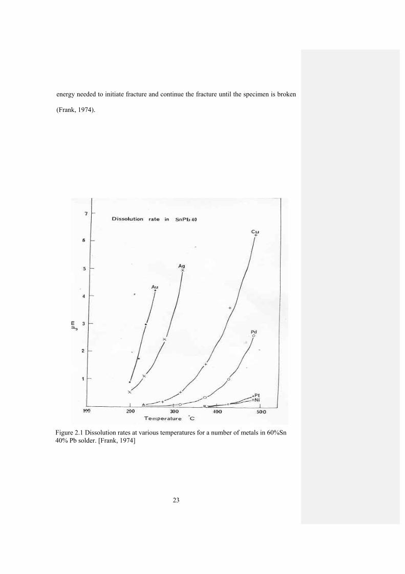
(Frank, 1974). Gold has the highest dissolution rate in solder compared to metals like
Ag, Cu, Pd and Ni (Refer to Figure 2.1) and this had led to high formation of
intermetallic (IMC) formation. Figure 2.2(a) shows when gold amount increases to 8-
10 wt%, ductility drop to almost zero and he also found simultaneous increase in
hardness (Figure 2.2(b)). This would normally expect to lead to increase in tensile
strength, however strengthening was counteracted by simultaneous loss in ductility.
The study using impact test as in Figure 2.2(c) shows that 4% gold in 63-37 tin-lead
solder causes no deleterious effects, a 5% addition results in drop in impact strength
from 80 to about 25 in-lb. Izod Impact is a single point test that measures a materials
resistance to impact from a swinging pendulum. Izod impact is defined as the kinetic
Formatted: Bullets and Numbering
23
energy needed to initiate fracture and continue the fracture until the specimen is broken
(Frank, 1974).
Figure 2.1 Dissolution rates at various temperatures for a number of metals in 60%Sn 40% Pb solder. [Frank, 1974]
24
Figure 2.2 (a) Top: Influence of Gold content in 63%tin-37% lead solder on tensile strength ductility. (b)Middle: Diamond hardness of 63%tin-37% lead solder for various gold contents. (c)Bottom: Effect on impact strength of 63%tin-37% lead solder of increasing concentration of gold. [Frank, 1974]