Embed Size (px)
Citation preview
1
Electronic Supplementary Information
Solution-processable antimony-based light-absorbing materials beyond lead halide perovskitesKarunakara Moorthy Boopathia,†, Priyadharsini Karuppuswamya,b,c,†, Anupriya Singha, Chintam Hanmandlud, Lin Line, Syed Ali Abbasa,b,c, Chien Cheng Changf, Pen Cheng Wangb, Gang Lig,*, and Chih Wei Chua,d*
a Research Center for Applied Science, Academia Sinica, Taipei 115, TaiwanE-mail: [email protected]
b Department of Engineering and System Science, National Tsing Hua University, Hsinchu, 30013c Nano Science and Technology, Taiwan International Graduate Program, Academia Sinica and National Tsing Hua
University, Taiwand College of Engineering, Chang Gung University, Taoyuan City, Taiwane College of Mechanical Engineering, Guangxi University, 100, Daxue Dong Road, Nanning 530004, Chinaf Institute of Applied Mechanics, National Taiwan University, Roosevelt Road, Taipei 106, Taiwang Department of Electronic and Information Engineering, The Hong Kong Polytechnic University, Hung Hom, Kowloon, Hong
Kong, ChinaE-mail: [email protected]†These authors contributed equally to this work
Experimental section
Aqueous hydroiodic acid (HI) (57 wt.% in water), methylamine (CH3NH2, 40 wt.% in water), SbI3
(99.998%), dimethylformamide (DMF), dimethyl sulfoxide (DMSO), CsI (99.999%), and diethyl ether
were purchased from Alfa Aesar and used without further purification. MAI was purchased from
Lumitech, Taiwan. Poly(3,4-ethylenedioxythiophene):poly(p-styrene sulfonate) (PEDOT:PSS. Clevios
P) was bought from Heraeus (Germany).
Device fabrication: Solar cell: Indium tin oxide (ITO)–coated glass substrates (<10 sq–1, RiTdisplay)
were cleaned through sonication, once in detergent (20 min) and then twice in deionized (DI) water
(20 min each), and dried under N2 gas. The substrates were treated with ultraviolet (UV)/ozone for
15 min to clean the surfaces and also to improve the surface adhesion. PEDOT:PSS was spin-coated
(4000 rpm, 60 s) onto the ITO surfaces, followed by annealing (130 °C, 30 min). The substrates were
transferred to a glove box for deposition of the perovskite active layer through a single-step spin-
coating method. The MA3Sb2I9 material was prepared from different molar ratio of SbI3 and MAI in
the DMF. The Cs3Sb2I9 material was prepared from different molar ratio of SbI3 and CsI in the mixed
DMF: DMSO (1:3) solvent. All solutions were kept on a hot plate at 70 °C overnight. Different
volumes of HI was added before 60 min of spin coating in the precursor solution, and kept at room
temperature. Solution was spin-coated (6000 rpm) onto PEDOT:PSS and annealed directly at 70 °C
Electronic Supplementary Material (ESI) for Journal of Materials Chemistry A.This journal is © The Royal Society of Chemistry 2017
2
for MA3Sb2I9 and 150 °C for Cs3Sb2I9 for 30 min. A solution (20 mg/mL) of [6,6]-phenyl-C71-butyric
acid methyl ester (PCBM) in chlorobenzene (CB) and was spin-coated (4000 rpm, 40 s) onto the
perovskite layer, followed by annealing at 100 °C for 30 min. The device was completed through
sequential thermal evaporation of C60 (30 nm), 2,9-dimethyl-4,7-diphenyl-1,10-phenanthroline (BCP,
7 nm), and an aluminum electrode (100 nm) through a shadow mask under vacuum (pressure: 1 x 10–
6 torr). The active area of each device was 10 mm2.
Characterization: XRD patterns were recorded at room temperature using a Bruker D8 X-ray
diffractometer (2 range: 5–80°; step size: 0.008°) equipped with a diffracted beam monochromator
set for Cu Kα radiation ( = 1.54056 Å). SEM images were recorded using an FEI Nova 200 scanning
electron microscope (15 kV). Glass substrates spin-coated with PEDOT:PSS were used for XRD
measurements; ITO substrates spin-coated with PEDOT:PSS were used for recording SEM images.
Absorption spectra of the films were measured using a Jacobs V-670 UV–Vis spectrophotometer. XPS
was performed at room temperature using a PHI 5000 Versa Probe (ULVAC-PHI) apparatus equipped
with an Al Kα X-ray source (1486.6 eV). UPS was used to measure the valance band using He I
emission (21.2 eV, ~50 W) as the source of ultra-violet light, and the take-off angle was 90°. EQE
spectra were recorded under short-circuit conditions. Devices were encapsulated before they were
removed for EQE measurement. The light source was a 75 W Xe lamp (Enlitech, QE-R3011); the light
output from the monochromator was focused on the photovoltaic cell being tested (DC mode). The
devices were illuminated inside a glove box by the Xe lamp, which functioned as a solar simulator
(Thermal Oriel 1000 W) providing a simulated AM 1.5 spectrum (100 mW cm–2). The light intensity
was calibrated using a mono-silicon photodiode with a KG-5 color filter (Hamamatsu).
3
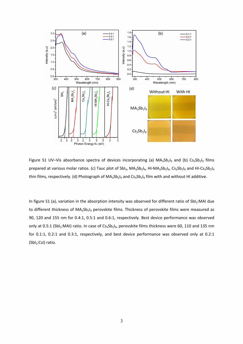
Figure S1 UV–Vis absorbance spectra of devices incorporating (a) MA3Sb2I9 and (b) Cs3Sb2I9 films
prepared at various molar ratios. (c) Tauc plot of SbI3, MA3Sb2I9, HI-MA3Sb2I9, Cs3Sb2I9 and HI-Cs3Sb2I9
thin films, respectively. (d) Photograph of MA3Sb2I9 and Cs3Sb2I9 film with and without HI additive.
In figure S1 (a), variation in the absorption intensity was observed for different ratio of SbI3:MAI due
to different thickness of MA3Sb2I9 perovskite films. Thickness of perovskite films were measured as
90, 120 and 155 nm for 0.4:1, 0.5:1 and 0.6:1, respectively. Best device performance was observed
only at 0.5:1 (SbI3:MAI) ratio. In case of Cs3Sb2I9, perovskite films thickness were 60, 110 and 135 nm
for 0.1:1, 0.2:1 and 0.3:1, respectively, and best device performance was observed only at 0.2:1
(SbI3:CsI) ratio.
4
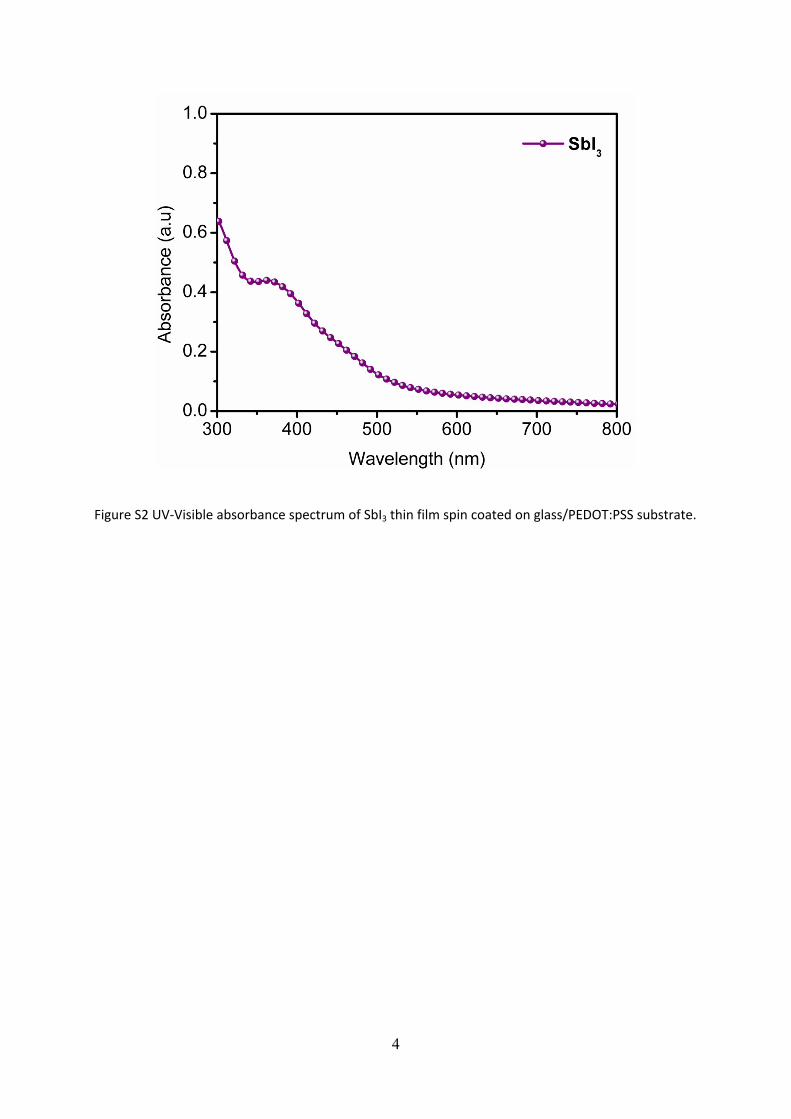
Figure S2 UV-Visible absorbance spectrum of SbI3 thin film spin coated on glass/PEDOT:PSS substrate.
5
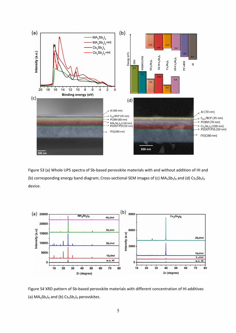
Figure S3 (a) Whole UPS spectra of Sb-based perovskite materials with and without addition of HI and
(b) corresponding energy band diagram; Cross-sectional SEM images of (c) MA3Sb2I9 and (d) Cs3Sb2I9
device.
Figure S4 XRD pattern of Sb-based perovskite materials with different concentration of HI additives
(a) MA3Sb2I9 and (b) Cs3Sb2I9 perovskites.
6
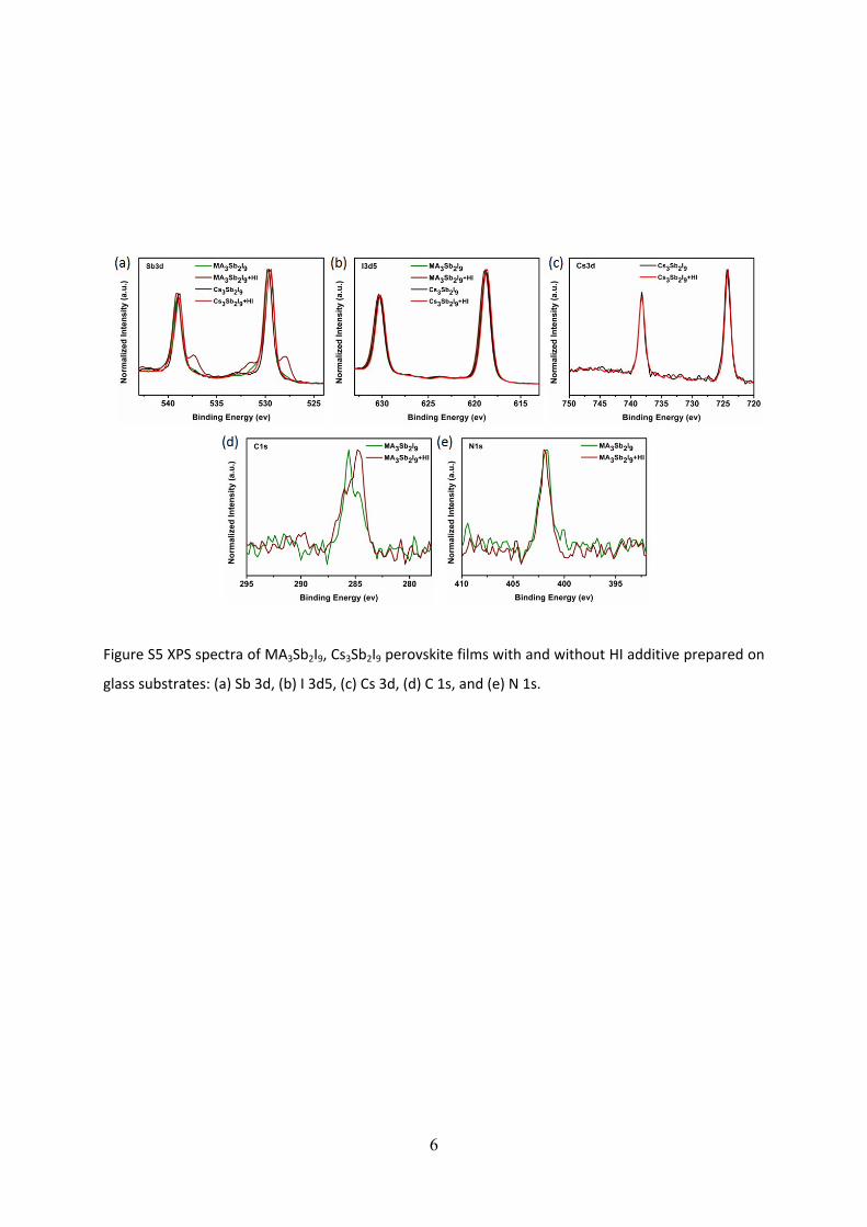
Figure S5 XPS spectra of MA3Sb2I9, Cs3Sb2I9 perovskite films with and without HI additive prepared on
glass substrates: (a) Sb 3d, (b) I 3d5, (c) Cs 3d, (d) C 1s, and (e) N 1s.
7
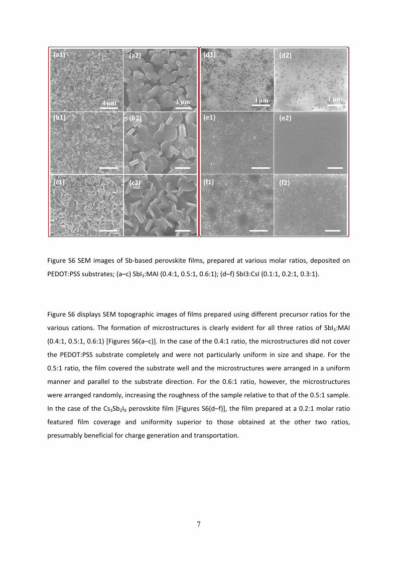
Figure S6 SEM images of Sb-based perovskite films, prepared at various molar ratios, deposited on
PEDOT:PSS substrates; (a–c) SbI3:MAI (0.4:1, 0.5:1, 0.6:1); (d–f) SbI3:CsI (0.1:1, 0.2:1, 0.3:1).
Figure S6 displays SEM topographic images of films prepared using different precursor ratios for the
various cations. The formation of microstructures is clearly evident for all three ratios of SbI3:MAI
(0.4:1, 0.5:1, 0.6:1) [Figures S6(a–c)]. In the case of the 0.4:1 ratio, the microstructures did not cover
the PEDOT:PSS substrate completely and were not particularly uniform in size and shape. For the
0.5:1 ratio, the film covered the substrate well and the microstructures were arranged in a uniform
manner and parallel to the substrate direction. For the 0.6:1 ratio, however, the microstructures
were arranged randomly, increasing the roughness of the sample relative to that of the 0.5:1 sample.
In the case of the Cs3Sb2I9 perovskite film [Figures S6(d–f)], the film prepared at a 0.2:1 molar ratio
featured film coverage and uniformity superior to those obtained at the other two ratios,
presumably beneficial for charge generation and transportation.
8
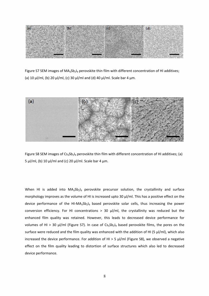
Figure S7 SEM images of MA3Sb2I9 perovskite thin film with different concentration of HI additives;
(a) 10 µl/ml, (b) 20 µl/ml, (c) 30 µl/ml and (d) 40 µl/ml. Scale bar 4 µm.
Figure S8 SEM images of Cs3Sb2I9 perovskite thin film with different concentration of HI additives; (a)
5 µl/ml, (b) 10 µl/ml and (c) 20 µl/ml. Scale bar 4 µm.
When HI is added into MA3Sb2I9 perovskite precursor solution, the crystallinity and surface
morphology improves as the volume of HI is increased upto 30 µl/ml. This has a positive effect on the
device performance of the HI-MA3Sb2I9 based perovskite solar cells, thus increasing the power
conversion efficiency. For HI concentrations > 30 µl/ml, the crystallinity was reduced but the
enhanced film quality was retained. However, this leads to decreased device performance for
volumes of HI > 30 µl/ml (Figure S7). In case of Cs3Sb2I9 based perovskite films, the pores on the
surface were reduced and the film quality was enhanced with the addition of HI (5 µl/ml), which also
increased the device performance. For addition of HI > 5 µl/ml (Figure S8), we observed a negative
effect on the film quality leading to distortion of surface structures which also led to decreased
device performance.
9
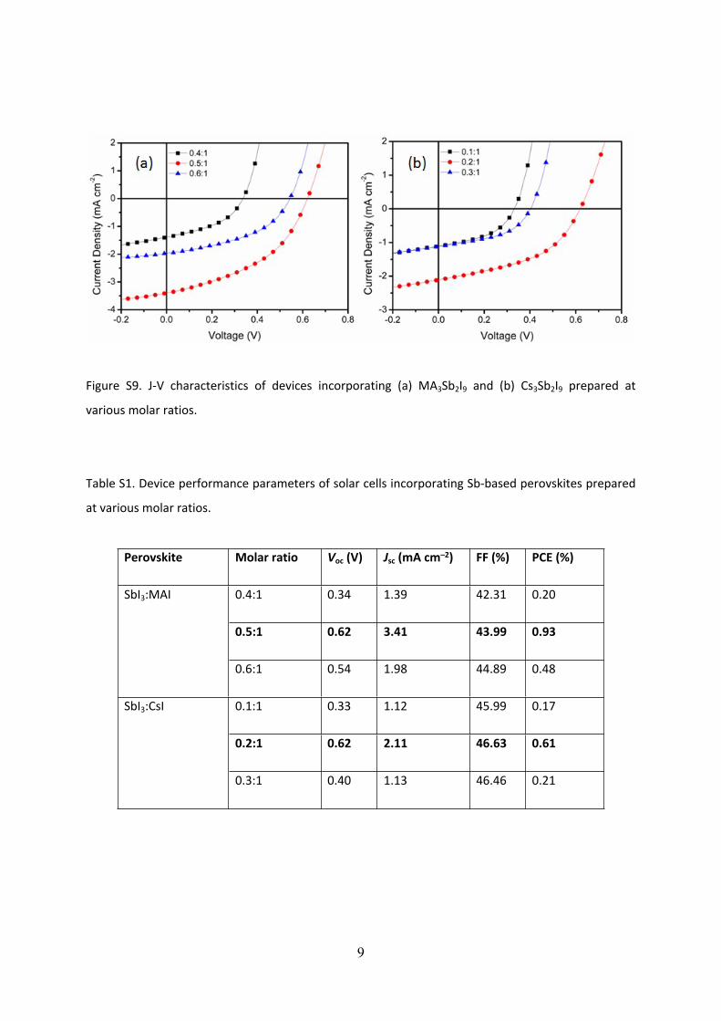
Figure S9. J-V characteristics of devices incorporating (a) MA3Sb2I9 and (b) Cs3Sb2I9 prepared at
various molar ratios.
Table S1. Device performance parameters of solar cells incorporating Sb-based perovskites prepared
at various molar ratios.
Perovskite Molar ratio Voc (V) Jsc (mA cm–2) FF (%) PCE (%)
0.4:1 0.34 1.39 42.31 0.20
0.5:1 0.62 3.41 43.99 0.93
SbI3:MAI
0.6:1 0.54 1.98 44.89 0.48
0.1:1 0.33 1.12 45.99 0.17
0.2:1 0.62 2.11 46.63 0.61
SbI3:CsI
0.3:1 0.40 1.13 46.46 0.21
10
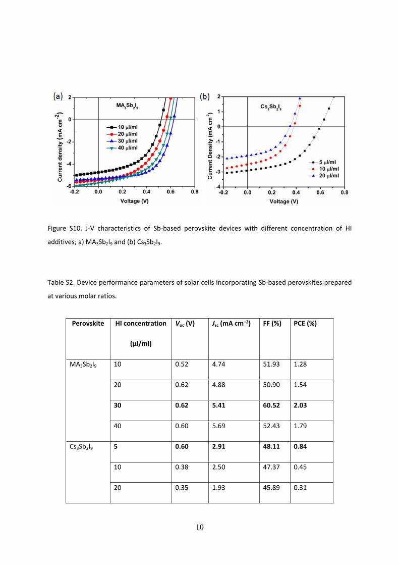
Figure S10. J-V characteristics of Sb-based perovskite devices with different concentration of HI
additives; a) MA3Sb2I9 and (b) Cs3Sb2I9.
Table S2. Device performance parameters of solar cells incorporating Sb-based perovskites prepared
at various molar ratios.
Perovskite HI concentration
(µl/ml)
Voc (V) Jsc (mA cm–2) FF (%) PCE (%)
10 0.52 4.74 51.93 1.28
20 0.62 4.88 50.90 1.54
30 0.62 5.41 60.52 2.03
MA3Sb2I9
40 0.60 5.69 52.43 1.79
5 0.60 2.91 48.11 0.84
10 0.38 2.50 47.37 0.45
Cs3Sb2I9
20 0.35 1.93 45.89 0.31
11
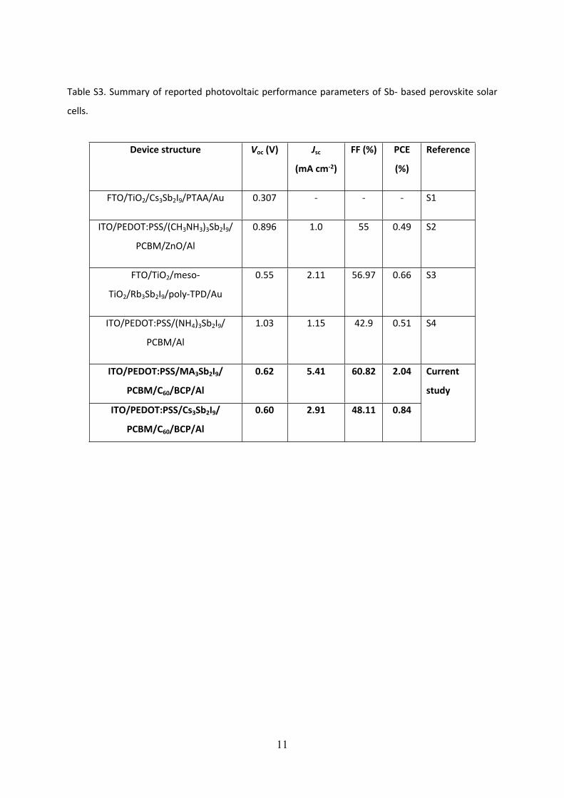
Table S3. Summary of reported photovoltaic performance parameters of Sb- based perovskite solar
cells.
Device structure Voc (V) Jsc
(mA cm-2)
FF (%) PCE
(%)
Reference
FTO/TiO2/Cs3Sb2I9/PTAA/Au 0.307 - - - S1
ITO/PEDOT:PSS/(CH3NH3)3Sb2I9/
PCBM/ZnO/Al
0.896 1.0 55 0.49 S2
FTO/TiO2/meso-
TiO2/Rb3Sb2I9/poly-TPD/Au
0.55 2.11 56.97 0.66 S3
ITO/PEDOT:PSS/(NH4)3Sb2I9/
PCBM/Al
1.03 1.15 42.9 0.51 S4
ITO/PEDOT:PSS/MA3Sb2I9/
PCBM/C60/BCP/Al
0.62 5.41 60.82 2.04
ITO/PEDOT:PSS/Cs3Sb2I9/
PCBM/C60/BCP/Al
0.60 2.91 48.11 0.84
Current
study
12
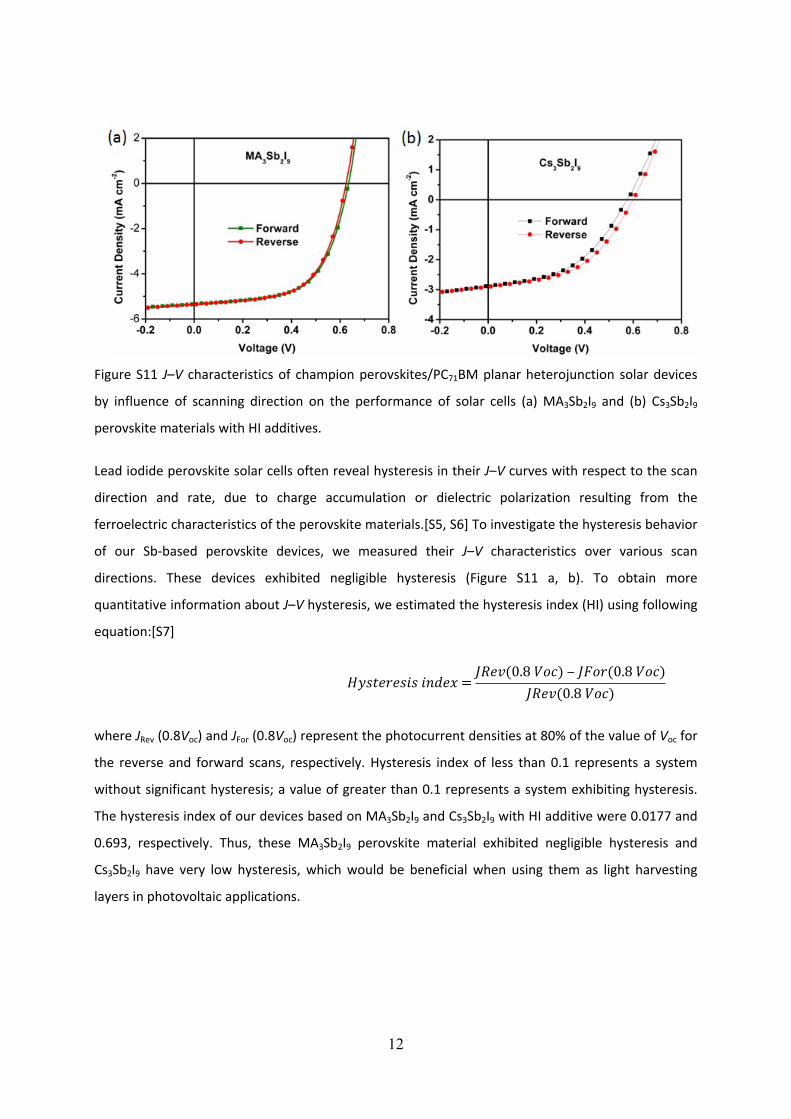
Figure S11 J–V characteristics of champion perovskites/PC71BM planar heterojunction solar devices
by influence of scanning direction on the performance of solar cells (a) MA3Sb2I9 and (b) Cs3Sb2I9
perovskite materials with HI additives.
Lead iodide perovskite solar cells often reveal hysteresis in their J–V curves with respect to the scan
direction and rate, due to charge accumulation or dielectric polarization resulting from the
ferroelectric characteristics of the perovskite materials.[S5, S6] To investigate the hysteresis behavior
of our Sb-based perovskite devices, we measured their J–V characteristics over various scan
directions. These devices exhibited negligible hysteresis (Figure S11 a, b). To obtain more
quantitative information about J–V hysteresis, we estimated the hysteresis index (HI) using following
equation:[S7]
𝐻𝑦𝑠𝑡𝑒𝑟𝑒𝑠𝑖𝑠 𝑖𝑛𝑑𝑒𝑥 =𝐽𝑅𝑒𝑣(0.8 𝑉𝑜𝑐) ‒ 𝐽𝐹𝑜𝑟(0.8 𝑉𝑜𝑐)
𝐽𝑅𝑒𝑣(0.8 𝑉𝑜𝑐)
where JRev (0.8Voc) and JFor (0.8Voc) represent the photocurrent densities at 80% of the value of Voc for
the reverse and forward scans, respectively. Hysteresis index of less than 0.1 represents a system
without significant hysteresis; a value of greater than 0.1 represents a system exhibiting hysteresis.
The hysteresis index of our devices based on MA3Sb2I9 and Cs3Sb2I9 with HI additive were 0.0177 and
0.693, respectively. Thus, these MA3Sb2I9 perovskite material exhibited negligible hysteresis and
Cs3Sb2I9 have very low hysteresis, which would be beneficial when using them as light harvesting
layers in photovoltaic applications.
13
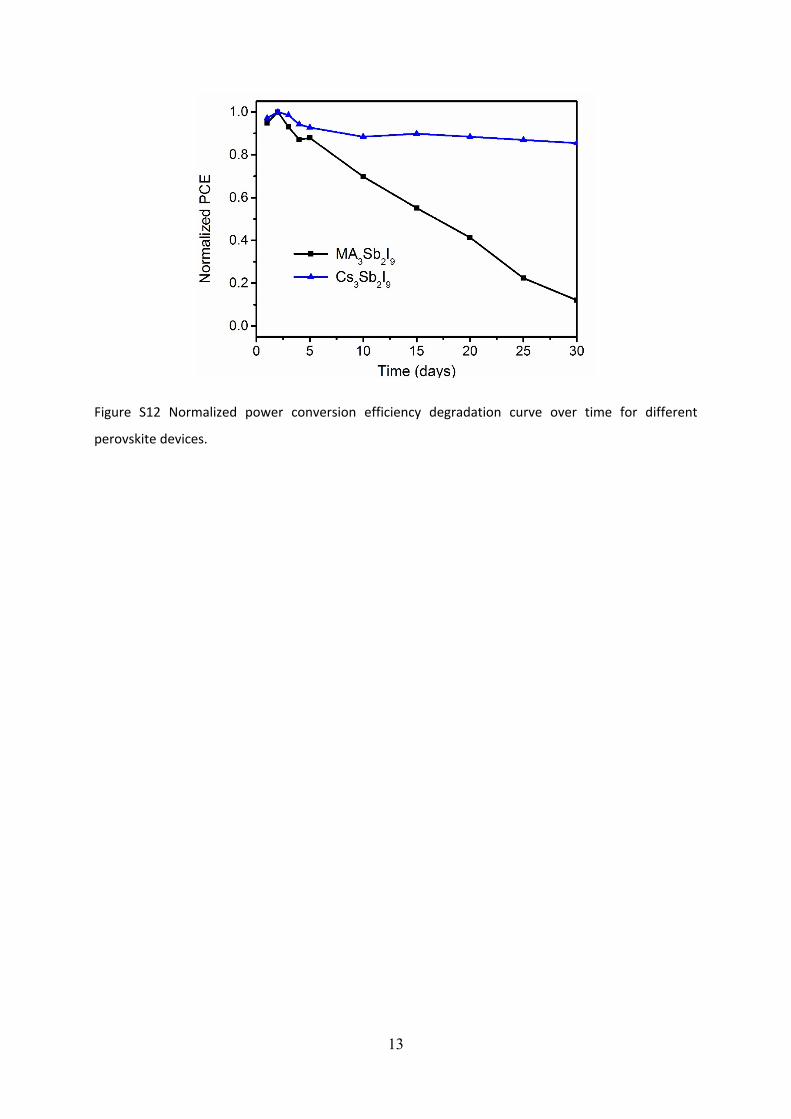
Figure S12 Normalized power conversion efficiency degradation curve over time for different
perovskite devices.
14
References
[S1] B. Saparov, F. Hong, J.-P. Sun, H.-S. Duan, W. Meng, S. Cameron, I. G. Hill, Y. Yan and D. B.
Mitzi, Chem. Mater., 2015, 27, 5622-5632.
[S2] J.-C. Hebig, I. Kühn, J. Flohre and T. Kirchartz, ACS Energy Lett., 2016, 1, 309-314.
[S3] P. C. Harikesh, H. K. Mulmudi, B. Ghosh, T. W. Goh, Y. T. Teng, K. Thirumal, M. Lockrey, K.
Weber, T. M. Koh, S. Li, S. Mhaisalkar and N. Mathews, Chem. Mater., 2016, 28, 7496-7504.
[S4] C. Zuo, L. Ding, Angew. Chem. Int. Ed., 2017, DOI: 10.1002/anie.201702265.
[S5] S. Meloni, T. Moehl, W. Tress, M. Franckevicius, M. Saliba, Y. H. Lee, P. Gao, M. K.
Nazeeruddin, S. M. Zakeeruddin, U. Rothlisberger and M. Graetzel, Nat. Commun., 2016, 7,
doi:10.1038/ncomms10334.
[S6] H. J. Snaith, A. Abate, J. M. Ball, G. E. Eperon, T. Leijtens, N. K. Noel, S. D. Stranks, J. T.-W.
Wang, K. Wojciechowski and W. Zhang, J. Phys. Chem. Lett., 2014, 5, 1511-1515.
[S7] H.-S. Kim and N.-G. Park, J. Phys. Chem. Lett., 2014, 5, 2927-2934.


![Electro‐Optic Modulation in Hybrid Metal Halide Perovskites · nonlinear crystals relies on costly and complicated bonding or deposition processes (heterogeneous integration).[4,5]](https://img.pdfslide.net/doc/110x75/5f3860b78cb5b531b06e28f0/electroaoptic-modulation-in-hybrid-metal-halide-perovskites-nonlinear-crystals.jpg)