Embed Size (px)
Citation preview

5274 | Mater. Adv., 2021, 2, 5274–5299 © 2021 The Author(s). Published by the Royal Society of Chemistry
Cite this: Mater. Adv., 2021,
2, 5274
Organolead halide perovskites beyond solar cells:self-powered devices and the associated progressand challenges
Avi Mathur, † Hua Fan† and Vivek Maheshwari *
Conventional electronic devices powered by lithium-ion batteries or supercapacitors face the challenge
of offering long-term and self-sustaining operations. Self-powered devices based on emerging energy
harvesting technologies can help of the development of long-lasting transducers with a small form
factor. Organolead halide perovskites due to their excellent electro-optical properties are promising
photosensitive materials for the development of such self-powered devices. The following review aims
at summarizing recent developments made in the field of organolead halide perovskite based self-
powered applications. The underlying mechanism driving the self-powered operation in electronic
devices such as photodetectors, tactile sensors, and gas sensors is discussed in detail. Finally, the
current challenges and prospects of these perovskite based optoelectronic applications are highlighted.
Introduction
With the ongoing continuous advancement in the fields of theInternet of Things (IoT),1–3 portable and wearable electronicdevices,4,5 structural monitoring,6,7 and implantable medical
devices,8,9 the indispensable dependence of electronic devicesand sensors on an external source of power poses a significantchallenge. As it stands, electronic devices and sensors, especiallythose located in remote places, are powered solely by batteries.The limited lifetime of batteries mandates frequent replacement,and, more importantly, batteries also pose a risk of leakingtoxic hazardous substances into the environment.10,11 Therefore,concurrently with the current efforts for the miniaturization ofsensors and integrated circuits,12 there is an equally critical needfor transducers that are capable of operating by harvesting power
Department of Chemistry, Waterloo Institute for Nanotechnology,
University of Waterloo, 200 University Ave. West, Waterloo, ON, N2L 3G1, Canada.
E-mail: [email protected]
Avi Mathur
Avi Mathur was born inKhairthal, India. He received hisBTech degree in information andcommunication technology andMTech degree in nanotechnologyfrom the University of Rajasthan,Jaipur. He is currently pursuing aPhD degree in chemistry(nanotechnology) from theUniversity of Waterloo, Canada.Before joining the doctoralprogram, Avi served as a ProjectResearch Assistant at theNanoscale Devices Laboratory,
Indian Institute of Science, Bangalore, India. He has authored 6original research articles so far. His research interests includeorganic–inorganic hybrid perovskites for photovoltaic and optoe-lectronic device applications.
Hua Fan
Hua Fan received her MS inapplied chemistry from BeihangUniversity in 2016. She iscurrently a PhD candidate inchemistry at the University ofWaterloo. Her research interestsinclude 1D nanomaterials,flexible devices, and wearableelectronics.
† A. M. and H. F. contributed equally to this work.
Received 24th April 2021,Accepted 28th June 2021
DOI: 10.1039/d1ma00377a
rsc.li/materials-advances
MaterialsAdvances
REVIEW
Ope
n A
cces
s A
rtic
le. P
ublis
hed
on 3
0 Ju
ne 2
021.
Dow
nloa
ded
on 3
/23/
2022
9:4
9:14
PM
. T
his
artic
le is
lice
nsed
und
er a
Cre
ativ
e C
omm
ons
Attr
ibut
ion
3.0
Unp
orte
d L
icen
ce.
View Article OnlineView Journal | View Issue
© 2021 The Author(s). Published by the Royal Society of Chemistry Mater. Adv., 2021, 2, 5274–5299 | 5275
solely from the ambient environment. Such an approach notonly will help in reducing the load drawn from batteries orsupercapacitors but can very well eliminate the need for anexternal power supply as well.
Self-powered devices, as the name indicates, do not need anexternal power source for their operation. They instead harvestenergy needed for their operation from the ambient environmentusing stimuli such as light, heat, mechanical modulations(e.g. vibrations, stress), and humidity variations.13 With theadvancement in the field of designing integrated circuits withlow power requirements, an increasing number of electronicdevices for a variety of applications are becoming feasiblecandidates to be self-powered.14–17 Owing to its ability to powerdevices and sensors even in outdoor and remote locations and itswidespread availability, light/solar energy harvesting provides aviable method for energy harvesting.18 Furthermore, presided bythe United Nations sustainability development goals, as we lookforward towards achieving modern, reliable, and cost-effectiveenergy for all, solar energy harvesting is being considered as oneof the most promising technologies for long-term renewableenergy production.19 In this pursuit, lead halide perovskitesare acknowledged as viable materials for the development ofcost-effective and highly efficient photovoltaic systems. The lastdecade has witnessed an intense research in perovskites solarcells (predominantly with lead-halide based materials), as theircertified power conversion efficiency (PCE) has exceeded 25%,up-scaled from just 3.8% within a decade, rivaling that of silicon-based solar cells.20,21 In general, perovskites refer to the class ofcompounds with a general formula of ABX3 where A and Brepresent cations of dissimilar sizes while X indicates anionhalides, sulfides, and oxides.22 Owing to their photosensitivenature, the focus of attention has been predominantly on theorganic–inorganic halide perovskites where A+ represents either amethylammonium (MA+) or formamidinium cation (FA+). Thesmall size of the methylammonium cation (CH3NH3
+) leads to theformation of a stable tetragonal phase at room temperature.23
The 3-D framework of MABX3 is devoid of distortion in theMA–X interaction, as otherwise observed in systems involvingethyl ammonium (CH3CH2NH3
+) and formamidinium cation
(HC(NH2)2+).24 In the context of occupying the B site in theABX3 system, lead (Pb) has been reported as the superiorconstituent in comparison to its IV A metal counterparts suchas tin (Sn), both in terms of stability and performance andconsequentially has been the most widely used metal ion.Ideally, utilization of those with lower atomic numbers (suchas Ge or Sn) can be used to lower the energy bandgap of thecorresponding perovskite and in addressing the toxicity of Pb,but their utilization is limited by the low intrinsic ionic stabilityof their divalent oxidation state.25 The halide anion X providesmuch more freedom of variation in its composition. Iodide (I),lying closest to Pb in the periodic table, shares a similarcovalent character and leads to a stable perovskite structure.Upon progressing down the VII A group elements (Cl - I), withan increase in the atomic size of the anion, the absorptionspectra shift towards a longer wavelength (redshift) which isattributed to a decrease in electronegativity.24 Hence, chlorideand bromide incorporation along with the iodide anion at the Xsite offers a facile way to tune the bandgap of the halideperovskites. Owing to the exhibition of remarkable propertiessuch as broad absorption spectrum, high absorptioncoefficient, long carrier lifetime, low trap density, and largediffusion length, organolead halide perovskites (OLHPs) areideally suited as a material of choice for photovoltaic devicesand light energy harvesting.26 For instance, the MAPbI3
tetragonal phase exhibits a suitable bandgap in the range of1.51–1.55 eV, with an 820 nm absorption edge, exceeding theoptimal 1.1–1.4 eV bandgap range governed by the Shockley–Queisser limit for a single-junction solar cell.27 Hence, MAPbI3
is the most typically employed OLHP in photovoltaicapplications.
While significant research efforts have been devoted toenhancing the PCE of perovskite solar cells (PSC), new applicationsof these materials are being researched with increasing efforts,for instance, lasers, light-emitting diodes (LEDs), photodetectors(PDs), gas sensors and tactile sensors.28–33 In the past fewyears, OLHP based optoelectronic devices and sensors, capableof operating without an external power supply and exhibitingexcellent performance, have been actively researched andreported, continuously advancing the field of self-powereddevices.34 Therefore, a review focusing on OLHP based self-powered devices will be useful for researchers in this field andalso the broader research community. This review provides adetailed discussion of the mechanisms driving self-poweredoperation in OHLP based electronic devices of varyingarchitecture and their associated figures of merit. Understandingthese ongoing developments of perovskite-based self-drivendevices will pave the way for further optimization andadvancements in this area for future commercialization. A widearray of applications beyond solar cells are discussed whereOLHP harvests energy and simultaneously serves as an activelayer in an integrated device. A limited discussion focuses oncases where OHLP harvests energy and drives an independentdevice. Primarily, the latest advancements in PDs, IoTs,transistors, photovoltachromic cells, and sensors are reviewed.Finally, the current challenges of the perovskite-based self-Vivek Maheshwari
Vivek Maheshwari is an associateprofessor of chemistry at theUniversity of Waterloo. He is also amember of the Waterloo Institute forNanotechnology. His group’sresearch is on lead halideperovskite materials for devices andsensors, 1D materials for wearabledevices, and nanomaterials forelectrocatalysis. He completed hisbachelor’s degree from the IndianInstitute of Technology, Delhi, andhis doctorate from Virginia Tech.
Review Materials Advances
Ope
n A
cces
s A
rtic
le. P
ublis
hed
on 3
0 Ju
ne 2
021.
Dow
nloa
ded
on 3
/23/
2022
9:4
9:14
PM
. T
his
artic
le is
lice
nsed
und
er a
Cre
ativ
e C
omm
ons
Attr
ibut
ion
3.0
Unp
orte
d L
icen
ce.
View Article Online

5276 | Mater. Adv., 2021, 2, 5274–5299 © 2021 The Author(s). Published by the Royal Society of Chemistry
powered devices are presented along with a discussion onfuture research prospects.
1. Photodetector (PD)
A PD converts an optical input such as visible light photons intoan electrical signal35 and has wide-ranging applications in thedetection of light intensity, spectral range detection,36 thermalimaging,37 remote imaging,38 and so forth. The significantfigures of merit for PDs include responsivity, detectivity, lightswitching ratio (on/off ratio), spectral selectivity, linear dynamicrange, and response time.39 Currently, most of the commercialphotodetectors are based on crystalline GaN, Si, and InGaAs.40
The underlying mechanism driving the PD operation is either ap–n (p–i–n) junction, Schottky based, or a photoconductiveeffect, where the conductivity of the active material increaseson interaction with the incident photons. Broad spectral range(190–1100 nm) commercial photodetectors based on the Si p–njunction (photodiodes) (e.g., Hamamatsu S1336) exhibit peakresponsivities of 0.12 and 0.5 A W�1 at 200 and 960 nm,respectively, and those designed especially for the visible range(340–720 nm) photometry (e.g., Hamamatsu S8265) exhibit aresponsivity of 0.3 A W�1 at the peak sensitivity wavelength of540 nm, with a dark current of B20 pA. These commercial PDsusually require an external power supply and hence need anintegrated assembly in the device which can make the devicebulky and serve as a bottleneck for utilization in a remotelocation. Furthermore, these commercial photodiodes needstringent manufacturing controls which limit them tolow-volume, high-value markets. To overcome the existingtrade-offs between performance, form factor, cost, and mostimportantly, power consumption, self-powered PDs are beinginvestigated with intense interest.41–43 Self-driven PDs can beobtained when photodiodes work at zero bias, similar to solarcells working under short-circuit conditions. Owing to theirexcellent electro-optical characteristics, the OLHP based self-powered PDs can offer the benefit of being lightweight with asmall device size, without compromising on deviceperformance.44 The early reports on perovskite-based PDs withself-powered characteristics (but did not focus on it exclusively)appeared in 2014 when Dou et al. demonstrated a solutionprocessed ‘inverted’ device (solar cell) configuration PD basedon organic–inorganic hybrid CH3NH3PbI3�xClx. The device hada high detectivity of up to 1014 Jones and was capable ofoperating at 0 V.45 Based on the charge separation mechanism,OLHP PDs can generally be classified into the followingcategories: p–n (or p–i–n) junction, Schottky junction, polarizationeffects based, and photoelectrochemical-type PDs. Besidesthese, an integrated system of energy harvesting units (suchas TENG) that drives the light sensitive OLHP to achievedetection can be considered as a distinct type of self-driven PD.The following section summarizes recent advances in PDs drivenby these operating mechanisms. Some common strategies thatare being employed for enhancing the figures of merit forperovskite PDs have also been discussed. The last subsection is
dedicated to flexible OLHP PDs that are now receiving substantialattention as promising candidates for next-generation portableand wearable electronics.
1.1 p–n (or p–i–n) junction-based PDs
The p–n junction-based PDs are the most common typereported so far in the literature. A typical PD with a verticalarchitecture consists of a perovskite layer sandwiched betweenan electron transport layer (ETL) and a hole transport layer(HTL) (p–i–n type). It is widely accepted that the interfacialcontact properties between the perovskite and transport layersaffect the efficiency of photovoltaic devices. Hence, by carefulselection of the transport layers, PDs with effective dissociationand transport of photogenerated charge carriers to their respectivecounter electrode contacts can be fabricated.46 ETLs not onlyinfluence the electron transfer and collection but also behave asthe hole blocking layer to suppress the electron–hole recombinationat the interface.47,48 Significant attention has been paid to ZnOas an electron transport material (ETL) in the early researchworks reporting OLHP based self-powered PDs. Specifically,morphological tuning of ZnO material was used for theperformance optimization of OLHP PDs. Initially, Wang et al.coupled the pyroelectric effect generated in wurtzite ZnOnanowires (NWs) with the photoexcitation ability of MAPbI3.49
The assembly with well-aligned energy band levels led toenhanced charge-carrier separation at the ZnO/perovskiteinterface. The perovskite also contributed to low dark currentsand low background temperature. In the self-powered mode, thisUV sensitive heterostructure assembly exhibited 322% enhancementin specific detectivity and responsivity, complemented with fiveorders of magnitude improvement in the rise time (5.4 s to53 ms) and fall time (8.9 s to 63 ms) in comparison to devicesoperating at an applied bias of 0.3 V. The decline in deviceperformance due to applied bias was attributed to the reducedpyro-potential of ZnO NWs owing to the high dark currents andhigh background temperature. Another report on well-alignedenergy levels in the ZnO nanorod (NR)/MAPbI3 heterostructureappeared a year later. Here, Yu et al. used an inorganic metaloxide layer of MoO3 as a hole transport layer to enhance excitontransport while simultaneously protecting the organicperovskite layer.50 The corresponding broadband PD with anappropriate thickness of MoO3 (12 nm) yielded a high detectivityvalue of 3.56 � 1014 Jones and 24.3 A W�1 photo-responsivityunder 500 nm excitation and no applied bias. Other thanpreferable band alignment, Zhu et al. proposed the hypothesisthat a uniformly distributed blend of ZnO microspheres andnanosheets can effectively utilize the high surface area ofmicrospheres while decreasing series resistance in a verticallyconfigured glass/fluorine doped tin oxide (FTO)/ZnO/MAPbI3/MoO3/Au device.51 Under illumination, the self-driven PDexhibited spectral response from 300 to 800 nm with responsivityand detectivity values reported as high as 48 mA W�1 and 4.5 �1011 Jones, respectively. The on/off ratio was up to 1400, whilethe rise time and fall time of the photoresponse were recordedto be 14 and 12 ms, respectively. Despite the facile synthesisprocess and high electron mobility with increased area of
Materials Advances Review
Ope
n A
cces
s A
rtic
le. P
ublis
hed
on 3
0 Ju
ne 2
021.
Dow
nloa
ded
on 3
/23/
2022
9:4
9:14
PM
. T
his
artic
le is
lice
nsed
und
er a
Cre
ativ
e C
omm
ons
Attr
ibut
ion
3.0
Unp
orte
d L
icen
ce.
View Article Online

© 2021 The Author(s). Published by the Royal Society of Chemistry Mater. Adv., 2021, 2, 5274–5299 | 5277
contact of the ZnO NR layer, the photoelectric performance ofPDs is generally limited. This is due to the presence of defectstates, especially oxygen vacancy which may lead to enhancedcharge recombination at the interface between perovskite andZnO NRs. To primarily reduce the defect density, Zhou et al.doped ZnO with a slightly smaller Ga3+.52 The Ga doped ZnO NRlayer (as ETL) served as an effective scaffold with enhancedelectron mobility. The resultant HTL-free PD device preparedusing graphite electrode had an on/off ratio, a responsivity, and adetectivity of B2.5 � 103, 0.3 A W�1, and 1.3 � 1012 Jones,respectively. The work by Yang et al. involved the coupling of aMgO/ZnO bilayer with the perovskite layer.53 The ZnO micro-sphere array scaffold facilitated the penetration of the perovskiteinto the array and resulted in improved light-harvesting, whileMgO passivated the interface between ZnO and perovskite,enhancing stability and carrier transport. Recently, Liu et al.proposed a Cu ion-induced p-type doping in perovskite films bythe addition of CuSCN.54 The CH3NH3
+ cations from theperovskite film reacted with the SCN� anions from the CuSCNdopant to form HSCN and CH3NH2 by-products, leaving Cu ionsto get incorporated into the final perovskite film. The p-typedoping facilitated hole transport at the p–n heterojunctioninterface of perovskite/[6,6]-phenylC61-butyric acid methyl ester(PCBM, ETL) in a self-powered HTL free PD. The authors utilizedthe optimized PD as a light signal receiver for transmitting textand audio signals in a homemade visible light communicationsystem. Zhou et al. coupled C60 as an ETL along with theperovskite/GaN heterostructure.55 A direct bandgap of 3.4 eVwith impressive electro-optical properties, a high carrier mobility,a high melting point, and the chemically stable nature (weakoxidation of N) motivated the authors to choose p-type GaN as theHTL in the hybrid perovskite PD. The high electron mobility andconductivity of C60 enhanced the collection of the electrons alongwith reduced non-radiative recombination enabling self-poweredcharacteristics. The best performing PD exhibited a responsivity of0.198 A W�1 and a detectivity of 7.96 � 1012 Jones with an on/offratio 45000. To achieve excellent PD device performance,selection of HTL is equally crucial, not only to extract the holesand decrease the dark current density but also to enhance andpromote perfect light absorption by the perovskite layer in thewhole visible region. Ghosh et al. fabricated an ETL-free self-biased PD inverted device by functionalizing HTL with plasmonicAg nanoparticles (NPs).56 The plasmon-enhanced opticalabsorption combined with improvement in charge extractionand transport by Ag NPs was attributed for the enhancedself-powered responsivity in the resultant PD (0.25 A W�1) witha detectivity as high as 1.53 � 1011 Jones. Shin et al. integratedgraphene quantum dots (QDs) in both the HTL and photoactiveMAPbI3 layer.57 The improved crystallinity of perovskite grainsupon the integration of graphene QDs was accredited to thepresence of hydrophilic groups including –OH, –COOH, andCQO that leads to the formation of strong bonds within theperovskite film. It was proposed that the addition of grapheneQDs increased the work function of the HTL leading to reducedcharge recombination at the perovskite/HTL interface. The corres-ponding self-powered rigid and flexible PDs exhibited detectivities
of 8.7 � 1012 and 8.42 � 1012 Jones, respectively, with an identicalresponse time of 0.96 ms at 0 V. The flexible PDs displayedappreciable bending stability by maintaining B80% of theiroriginal responsivity values after repeated bending for 1000 cyclesat a radius of 4 mm. Cheng et al. carried out hydrothermal etchingof monocrystalline silicon to prepare an array of silicon nano-porous pillars (Si-NPA) which was later used as a substrate as wellas a HTL in an inverted assembly of Si-NPA/MAPbI3/ZnO PD.58
The air-stable inorganic HTL enabled the PD to retain 92%performance despite storing the device in ambient air for amonth. The template of quasi-identical micron-sized Si pillarsoffered a large interfacial contact area for incident light whilesimultaneously reducing the reflection. The authors proposedthat the Si-NPA template also effectively enhanced carriertransport and reduced the collection path of the photogeneratedcarriers leading the self-driven PDs to exhibit a high on/off ratio of8.2 � 104, a photoresponsivity of 8.13 mA W�1, a specificdetectivity of 9.74 � 1012 Jones, and fast response speeds of253.3/230.4 ms at zero bias under 780 nm light illumination.
Towards realizing the commercial applications of self-drivenPD based on OLHP, the work of Shen et al. can be considered asone of the most significant contributions. The authors demon-strated a homemade time-resolved photoluminescence (TRPL)system (Fig. 1a) facilitated by an ultrafast OLHP PD with theconfiguration of indium tin oxide (ITO)/poly(bis(4-phenyl)(2,4,6-trimethylphenyl)amine) (PTAA)/MAPbI3/C60/2,9-dimethyl-4,7-diphenyl-1,10-phenanthroline (BCP)/copper (Cu).59 The devicearea dependent sub-nanosecond response time (0.95 ns for0.04 mm2 device area) of the PD enabled the detection of thephotoluminescence lifetime for typical organic and hybridmaterials, ranging from several nanoseconds to microseconds(Fig. 1b–d). In a recent work, Shan et al. presented a bifunctionallight-emitting/detecting LiFi (light fidelity) fiber utilizingperovskite QDs.60 The authors capitalized on the small excitonbinding energy and high carrier mobility of the all-inorganicperovskite QDs (CsPbBr3) to successfully integrate electrolumines-cence with narrow emission (B19 nm) and photodetection in asingle fiber. The flexible assembly exhibited green coloredluminance of B100 cd m�2 at 7 V after being subjected tomultiple bending cycles and the corresponding current efficiencywas 1.67 cd A�1. The band bending in the space charge region atthe interface between the perovskite QDs and the transport layers(due to differences in the Fermi levels) enabled a zero-biasoperation of the PD with an on/off ratio of 1.5. OLHP QDs canpotentially be utilized based on a similar principle for bi-functional devices. A major challenge that hinders thecommercial viability of OLHP PDs (and other devices) is theirinstability in air and under ambient conditions. OLHP materialrapidly degrades and decomposes in the presence of oxygen andmoisture. Furthermore, electric field induced ion migrationprimarily across the perovskite grain boundaries further enhancesmaterial degradation, eventually worsening the optoelectronicproperties.61 However, at the same time, the C-AFM andPC-AFM studies carried out by Li et al. in MAPbI3/CdS hetero-junction PD indicated that a short transport distance at thegrain boundaries acted as preferential spots of charge carrier
Review Materials Advances
Ope
n A
cces
s A
rtic
le. P
ublis
hed
on 3
0 Ju
ne 2
021.
Dow
nloa
ded
on 3
/23/
2022
9:4
9:14
PM
. T
his
artic
le is
lice
nsed
und
er a
Cre
ativ
e C
omm
ons
Attr
ibut
ion
3.0
Unp
orte
d L
icen
ce.
View Article Online

5278 | Mater. Adv., 2021, 2, 5274–5299 © 2021 The Author(s). Published by the Royal Society of Chemistry
transportation and exciton separation.62 The study of the photo-electric mechanism at the nanoscale showed that higher photo-current values are observed at the grain edges. This offers thepotential of grain boundary engineering towards fine-tuningthe overall device performance. The fabricated PD exhibited ahigh current on/off ratio of B1.13 � 105, detectivity of B9.79 �1010 Jones, and PCE of up to B10.05%. Table 1 summarizesthe heterojunction based self-powered OLHP PDs and theirassociated key figures of merit.
Although the p–n junctions have been widely applied in thefabrication of OLHP based self-driven PDs, little attention hasbeen paid to the formation of the p–n homojunction withinOLHP. Pang et al. stressed that the transport layers are optional
in perovskite-based optoelectronic devices and claimed that theintrinsic light-induced self-poling ability in the perovskitecould drive a Pt/CH3NH3PbI3/SiO2/Si/Al configured PD.63
The researchers through series of experiments ruled out thepossibility of the observed self-powered characteristics beingdriven by the Schottky junction or poling of the device(by applying an external bias for a short duration beforerecording the device characteristics at 0 V). The authorshypothesized that under illumination, a built-in electricfield was generated as positive ions/vacancies accumulated atthe perovskite/SiO2 interface and negative ions/vacanciesaccumulated at the perovskite/Pt interface, owing to bandbending in the asymmetric device. Under the influence of the
Fig. 1 Homemade time-resolved photoluminescence lifetime (TRPL) detection system with OLHP PD: (a) layout of the TRPL system. The N2 ns laseracted as an excitation source for illuminating the sample from a small angle located at the focus position of Lens 1. The OLHP photodetector receivesphotoluminescence from the sample once redirected by Lens 2. A filter was incorporated to filter the laser scattering emission. A 1 GHz oscilloscope witha 50 O input resistance was connected to the PD to record the transient photocurrent curves. PL decay curves measured by homemade and commercialTRPL systems for (b) green polyfluorene (4.0 ns), (c) MAPbBr3 single crystal (60.0 ns) and (d) bis(2-methyldibenzo[f,h]quinoxaline) (acetylacetonate)iridium(III) (1.0 ms). The solid line is representative of exponential fitting to the data. Reproduced with permission from Shen et al., Adv. Mater., 28, 10794–10800.59 r 2016 Wiley-VCH Verlag GmbH & Co. KGaA, Weinheim.
Table 1 Summary of the p–i–n/n–i–p heterojunction based OLHP self-driven PDs and their device characteristics
Device architectureOperatingwavelength Responsivity
Detectivity(Jones)
Light switchingratio
Response speed(rise/fall time) Ref.
FTO/ZnO/MAPbI3/Spiro-OMeTAD/Cu 325 nm 26.7 mA W�1 4.0 � 1010 53/63 ms 49FTO/ZnO NR/MAPbI3/MoO3/Au 500 nm 24.3 A W�1 3.56 � 1014 0.7/0.6 s 50FTO/ZnO/MAPbI3/MoO3/Au 380 nm 48 mA W�1 4.5 � 1011 1400 14/12 ms 51FTO/Ga3+ doped ZnO NR/MAPbI3/MoO3/Au 490 nm 0.3 A W�1 1.3 � 1012 B2.5 � 103 o2/o2 ms 52FTO/ZnO/MgO/MAPbI3/C 473 nm 5.9 � 10�2 A W�1 1.5 � 1012 7.0 � 104 0.63/1.6 ms 53ITO/MAPbI3:CuSCN/PCBM/BCP/Ag 685 nm 0.37 A W�1 1.06 � 1012 5.02/5.50 ms 54FTO/C60/MAPbI3/GaN 500 nm 0.198 A W�1 7.96 � 1012 45000 0.45/0.63 s 55FTO/PEDOT:PSS + Ag NPs/CH3NH3PbI3/Al 400 nm 0.25 A W�1 1.53 � 1011 110/72 ms 56Al/BCP/PCBM/MAPbI3:GQDs/PEDOT: GQDs/TFSA-GR 430 nm 0.435 A W�1 8.7 � 1012 0.56/0.96 ms 57Planar Si/Si-NPA/MAPbI3/ZnO 780 nm 8.13 mA W�1 0.974 � 1013 0.82 � 105 253.3/230.4 ms 58ITO/PTAA/MAPbI3/C60/BCP/Cu 680/700 nm 0.47 A W�1 (�0.1 V) 7.8 � 1012 (�0.1 V) 0.95 ns 59ITO/CdS/MAPbI3/Au 730 nm 0.43 A W�1 2.3 � 1011 1.13 � 105 3.2/9.6 ms 62
Materials Advances Review
Ope
n A
cces
s A
rtic
le. P
ublis
hed
on 3
0 Ju
ne 2
021.
Dow
nloa
ded
on 3
/23/
2022
9:4
9:14
PM
. T
his
artic
le is
lice
nsed
und
er a
Cre
ativ
e C
omm
ons
Attr
ibut
ion
3.0
Unp
orte
d L
icen
ce.
View Article Online

© 2021 The Author(s). Published by the Royal Society of Chemistry Mater. Adv., 2021, 2, 5274–5299 | 5279
built-in electric field, the photogenerated charge carriersdrifted to their respective counter electrodes. While the holeswere collected by the Pt electrode, the electrons traversedthrough the SiO2 film and were collected by the Al electrodeby the ion trap-assisted emission mechanism (Frenkel–Pooleemission). By contrast, under the dark conditions, SiO2 effectivelyacted as an insulating layer and functioned as a barrier layer forcarriers, leading to ultralow dark currents. The detectivity of thefabricated self-powered PD was measured to be 8.8 � 1010 Joneswith a high on/off ratio of 105 at 0 V. In a separate work, Ren et al.deliberately transformed the top surface of the p-type perovskite(MA+ rich and Pb2+ deficient stoichiometry) to n-type viabombarding with Ar+ ions leading to the formation of a p–nhomojunction within the perovskite layer.64 The resultant built-infield in the perovskite promoted the separation and transport ofphoto-induced carriers without any external bias. The Ar+ ionbombarding facilitated MAPbI3 p–n homojunction PD exhibitedan increase by one order of magnitude in the on/off ratio at532 nm in comparison to the pristine MAPbI3 device.
1.2 Schottky junction-based PDs
A typical PD assembly incorporating a photosensitive semi-conducting material with two ohmic metal contacts requires anexternal bias to drive the separation of the photogeneratedelectron–hole pairs. However, if one of the Ohmic contacts isreplaced by a Schottky barrier contact, the built-in electricalfield at that interface can lead to the separation of the photo-generated charge carriers. Unlike PDs with Ohmic contacts, theSchottky junction PDs, therefore, offer the ability to detect lightirradiation without an external power supply and with highsensitivity and response speed complemented by the low darkcurrents. Multiple reports demonstrating the Schottky junctionfacilitated self-driven PDs are found in the literature. As aseminal work, the Schottky junction photodiode of the ITO/MAPbI3/Au vertical heterostructure assembly presented byPandey et al. exhibited a photosensitivity of 1.33 � 102 withthe rise time and decay time of 91 and 101 ms, respectively.65
Subsequently, several important works on high-detectivity andlow-noise perovskite photodiodes were reported by differentresearch groups. The ultrahigh mobility and conductivity ofmultilayer graphene and its ability to form a Schottky barrierwith TiO2 were combined with the high yield photocarriertransport and strong broadband light absorption capability(260–900 nm) of CH3NH3PbI3, by Li et al.66 Both grapheneand perovskite act as ambipolar materials and therefore,depending on the inherent Schottky field, electrons could betransferred vertically from perovskite to TiO2 via the underlyinggraphene while the remnant holes remaining in the graphenewere transferred horizontally and collected in a separate FTOelectrode. The self-driven PD (FTO/TiO2–Graphene/MAPbI3/PTAA) demonstrated a high responsivity (B0.375 A W�1) andspecific detectivity (B1011 Jones) and an excellent on/off ratioof 4 � 106 in comparison to the commonly used Au–perovskite–Au configuration. The protection by the top PTAA layer enablednegligible decay in the performance of the PD despite storage
under ambient conditions for 20 days and stability over1000 cycles of operation.
Other than graphene, 2D transition-metal dichalcogenides(TMDs) are being extensively researched for a wide array ofpotential applications, including optoelectronics, biosensors,and piezoelectricity.67–72 As a typical TMD material, MoS2 hassuitable band levels and excellent charge transport properties,thus, is well suited to construct PDs based on the Schottkyeffect.73 Bai et al. were amongst the first ones to use single-layerMoS2 and MAPbI3 perovskite heterojunction in a verticallyconfigured PD.74 At a light intensity of 0.7 mW cm�2, the self-powered PD exhibits a responsivity of 60 mA W�1 with aninverse relation to power density. Zeng et al. combined multi-layered PdSe2, another TMD material, with FA1�xCsxPbI3
perovskite to achieve a Schottky junction empowered fast self-driven PD with broad spectral sensitivity (200–1550 nm).75
Fig. 2a provides the schematic illustration and Fig. 2b–lrepresents the optoelectronic response of the PdSe2/perovskiteSchottky junction PD device. The high carrier mobility of PdSe2
and reduced surface defects at the TMD/perovskite interfaceenabled the Schottky junction-based PdSe2/perovskite PD toexhibit a large on/off ratio of B104, a high responsivity of313 mA W�1 (Fig. 2j and l), a specific detectivity of B1013 Jones(Fig. 2l), and rapid response speeds of 3.5/4 ms. Moreover, thedevice exhibited sensitivity to polarized light, with a polarizationsensitivity of 6.04 (Fig. 2m). To explore the infrared imagesensing ability of the fabricated PD, homemade masks in theshape of alphabets such as P, O, L, Y, and U were placed betweenthe laser illumination and the device as seen in Fig. 2n. Theauthors were then able to generate a 2D contrast mapping profileby plotting the dark current and photocurrent of the PD, at eachpixel. Since the pixel illuminated by an 808 nm light demon-strated a considerable photocurrent of B0.05 mA, while the restof the area displayed negligible dark currents, the authors wereable to establish that the Cs-doped FAPbI3 PD could effectivelyresolve images under infrared illumination (Fig. 2o).
1.3 Ferroelectric and polarization effect based PDs
Ferroelectrics present a promising alternative for generatingpower in single-phase homogeneous materials by usingpolarization to trigger light detection. However, the presence ofthe ferroelectric polarization effect in OLHP is still debatable.76–81
Saraf et al. discussed the interplay between the polarization effectand ion migration as a function of poling conditions in MAPbI3
based PD (Fig. 3a).82 The work supported the presence offerroelectric effect in MAPbI3 as the PD poled under air andillumination lead to a ferroelectric dominated response, whilepoling under N2 and dark conditions leads to ion migrationeffects resulting in the formation of a p–n homojunction whichis signified by a reversal in signs for open-circuit voltage (Voc) andshort circuit current (Isc) as observed in Fig. 3b–e. To obtain astable response, poling was done under a small external biasapplied across the Au/MAPbI3/Au configuration in air and underillumination for a short duration of 10 minutes. The poleddevice could then operate without requiring an external powersupply for the next 2 days. Besides, the authors adopted an
Review Materials Advances
Ope
n A
cces
s A
rtic
le. P
ublis
hed
on 3
0 Ju
ne 2
021.
Dow
nloa
ded
on 3
/23/
2022
9:4
9:14
PM
. T
his
artic
le is
lice
nsed
und
er a
Cre
ativ
e C
omm
ons
Attr
ibut
ion
3.0
Unp
orte
d L
icen
ce.
View Article Online

5280 | Mater. Adv., 2021, 2, 5274–5299 © 2021 The Author(s). Published by the Royal Society of Chemistry
additive engineering strategy of integrating polystyrene (PS) inthe MAPbI3 films to enhance their stability. The PS–MAPbI3
based planar configuration PD device illustrated an impressive
performance stability of 480% post 20 days. On the other hand,the pristine MAPbI3 counterpart device suffered from a 70–85%performance decay within 4 days of operation under similar
Fig. 2 Schematic illustration and optoelectronic measurement of the PdSe2/perovskite Schottky junction PD: (a) schematic of polarized detectiondevice based on PdSe2/perovskite. (b) I–V curve in dark and under illumination with different lights. (c) Wavelength-dependent EQE at 0 V. Spectralphotoresponse in the self-powered mode under (d) 200 nm (3.72 mW cm�2) and (e) 1550 nm (0.82 mW cm�2) light illuminations. (f) Independent UV-Visabsorption spectrum of PdSe2, perovskite, and PdSe2/MAPbI3. (g) I–V curves of PD in dark and under an 808 nm light irradiation with different intensities.(h) Time-dependent photocurrent under an 808 nm light illumination with different light intensities. (i) Photocurrent and on/off ratio as a function of lightintensity at zero bias. (j) Responsivity and detectivity as a function of incident power intensity. (k) Time-dependent photocurrent at reverse bias under an808 nm light illumination (0.3 mW cm�2). (l) Responsivity and detectivity as a function of operating bias voltage (0.3 mW cm�2). (m) Evolution ofphotocurrent as a function of different polarized angles. (n) Homemade experimental setup to realize detection ability of PdSe2/OLHP PD for NIR imagingsensing. (o) The corresponding 2D current mapping of characters ‘‘P,’’ ‘‘O,’’ ‘‘L,’’ ‘‘Y,’’ and ‘‘U’’ produced by an 808 nm laser. Reproduced from Zeng et al.,Adv. Sci., 6, 1901134.75 r 2019 WILEY-VCH Verlag GmbH & Co. KGaA, Weinheim.
Materials Advances Review
Ope
n A
cces
s A
rtic
le. P
ublis
hed
on 3
0 Ju
ne 2
021.
Dow
nloa
ded
on 3
/23/
2022
9:4
9:14
PM
. T
his
artic
le is
lice
nsed
und
er a
Cre
ativ
e C
omm
ons
Attr
ibut
ion
3.0
Unp
orte
d L
icen
ce.
View Article Online

© 2021 The Author(s). Published by the Royal Society of Chemistry Mater. Adv., 2021, 2, 5274–5299 | 5281
ambient conditions. The monolith PD achieved a photorespon-sivity of more than 0.61 A W�1 and a detectivity of 1.5� 1013 Jonesunder such self-powered operation. Recently, utilizing the samedevice architecture and self-powered mechanism, Mathur et al.,unveiled the nanoscale tri-layer architecture of the polymer-perovskite (PS–MAPbI3) films in which the polymer forms a thinlayer at the top and bottom interfaces while the perovskite formsbulk of the interlayer.83 It was observed that the viscosity of thepolymer chains, directly dependent on the molecular weight (Mw)of the integrated polymer, is critical in determining the chainmobility and drives the rearrangement of the polymer chainsacross the perovskite film. Not only does the inclusion of varyingMw of PS (2.5, 11, 35, 61, 105, and 190 kDa) modulate thecrystallization kinetics but the insulating nature of the polymer
chains also affects the charge transport. The presence of PSchains, predominantly at the grain boundaries reduces ionmobility and hence leads to reduced dark currents and ioniccurrents. Overall, the inclusion of intermediate Mw PS chains of35 kDa led to optimized electro-optical properties with enhancedstability in the corresponding self-powered PD. Specifically, a3-fold enhancement in Isc (96.6 nA) and Voc (162.5 mV) wasobserved for 35 kDa PS–MAPbI3 PD in comparison to pristineMAPbI3 (31.1 nA and 52.3 mV, respectively).
Irrespective of the debatable existence of ferroelectricpolarization in perovskites, incorporation of an additional layerof a ferroelectric material in the perovskite PD architecturecan enhance the built-in electric field leading to improvedcharge extraction. A report demonstrating polarization induced
Fig. 3 Device architecture and photoresponse after poling of MAPbI3 based PD in different environments: (a) schematic diagram of the lateral self-powered PD and the effect of electric field poling leading to Voc and Isc response at zero bias. The Isc response at 0 V from (b) MAPbI3, and (c) PS–MAPbI3devices to various light illumination intensities, post poling at different voltages for 10 min in air and under light illumination (1.0 sun). The Isc response atzero bias from (d) MAPbI3 and (e) PS–MAPbI3-based PDs at various light intensities after poling at different voltages under N2 and dark. Reprinted withpermission from R. Saraf and V. Maheshwari, ACS Appl. Mater. Interfaces, 10, 21066–21072.82 Copyright r 2018 American Chemical Society.
Review Materials Advances
Ope
n A
cces
s A
rtic
le. P
ublis
hed
on 3
0 Ju
ne 2
021.
Dow
nloa
ded
on 3
/23/
2022
9:4
9:14
PM
. T
his
artic
le is
lice
nsed
und
er a
Cre
ativ
e C
omm
ons
Attr
ibut
ion
3.0
Unp
orte
d L
icen
ce.
View Article Online

5282 | Mater. Adv., 2021, 2, 5274–5299 © 2021 The Author(s). Published by the Royal Society of Chemistry
internal electric field in a perovskite-based device appeared in2018 where Cao et al. integrated ferroelectric SrTiO3 (STO) toserve as an interlayer in a sandwich structure of FTO/STO/MAPbI3/Spiro-OMeTAD/Ag.84 The polarized STO layer providesa built-in potential and promotes downward band bending,helping to separate and transport charge carriers generated inMAPbI3 upon illumination. Upon optimization of the STO layerdensity, the photocurrent was enhanced up to 0.956 mA withresponse speeds of 0.3 s (rise time) and o0.1 s (decay time) at0 V in a PD positively poled at 1 V for 5 min. However, unlikethe report of Saraf et al., there was an obvious decrease inphotoresponse upon exposure to air for 24 h. The substantialperformance decay can be attributed to the decomposition anddegradation of the OLHP active layer which is indicative ofthe limited stability of the fabricated PD. The authors laterdemonstrated a poling induced self-driven bulk heterojunctionPD. This research involved the integration of another ferroelectricmaterial P(VDF-TrFE) to enhance the strength of the ferroelectricfield of the perovskite layer, facilitating better separation ofthe photogenerated charge carriers.85 The corresponding PDexhibited high responsivity (20 mA W�1), large detectivity (1.4 �1013 Jones), and fast response speed (92/193 ms) at the wavelengthof 650 nm. Later, the group extended the same compositeassembly in the form of a nanowire array via an imprintingmethod assisted by commercially available digital versatile discs(DVD).86 The resultant flexible hybrid device on the PEN substrateexhibited high detectivity (7.3 � 1012 Jones), fast response time(88/154 ms) at zero bias, and impressive mechanical stabilitythrough bending up to 180 degrees.
1.4 Triboelectric nanogenerator (TENG) based PDs
Triboelectric nanogenerators (TENGs) can act as an efficientdriving source for harvesting mechanical energy to powerdevices such as PDs. When a physical contact occurs at theinterface of two dissimilar materials, typically opposite tribo-electric charges are created on the two surfaces. A mechanicalmotion can then induce an inherent electric potential differencecapable of driving electrons back and forth between the electrodes.Su et al. fabricated a UV-Visible broad range PD based on the dualproperties of MAPbI3: photoconductivity and surface triboelectriccharge density.87 An oscillating Voc was generated upon the topcopper electrode periodically getting into contact with theunderlying perovskite layer. Upon photoexcitation, electronsfrom the photogenerated electron–hole pair got quicklycaptured by the mesoporous TiO2 layer, while holes tend topartially neutralize the negative triboelectric charges present onthe surface leading to an instantaneous decrease in surfacecharge density. The corresponding device demonstrated aresponsivity of 7.5 V W�1 with a response time of o80 ms.Later, Hsiao et al. demonstrated a similar TENG assistedperovskite PD that could generate photo response uponbending of the flexible assembly.88 Guo et al. designed a self-powered organic optical communication system (SOCS).89 Thissystem was composed of organic light-emitting diode (OLED)driven by triboelectric nanogenerators (TENGs) and perovskitePD. In this SOCS, the mechanical signals were converted into
light by the OLED and then transferred to voltage signals by theperovskite PD. The combination of TENG with OLED exhibitingan emission peak at B524 nm served as a light emitter in therobotic hand, while PD served as the output voltage of SOCSwith a maximum current transfer ratio of 30%. The outputvoltage of SOCS was modified by the different mechanicalactions of the robotic hand which could be used to transmitthe information on human–machine interaction.
One of the biggest limitations of conventional TENG-powered devices is their dependency on motion actuators as apower source which are prone to fluctuations due to variationin the surrounding conditions, severely hindering the accuracyof photodetection. The self-powered PD reported in work byLeung et al. aimed at mitigating this issue by excludingmechanical pressure being applied to the TENG (Fig. 4a–c).90
The PD instead utilized the voltage regulated circuit containinga resistor and a Zener diode, which enabled uniform photo-detection characteristics irrespective of irregular motion, suchas human finger tapping (Fig. 4d). The fundamental principlecomprised perovskite acting as a variable resistor dependent onthe incident light intensity. The voltage in the photosensitivelayer followed an inverse relation with light intensity owing to adecrease in resistivity by the photogenerated carriers (Fig. 4eand f). The flexible and transparent polymer architecture of thePD empowered a stable device performance after 1000 bendingcycles and photosensitivity at 360 degrees of illumination(Fig. 4j). The self-powered PD exhibited an impressive maximumvoltage responsivity of 79.4 V mW�1 cm�2 and a B90% changein voltage at an incident light intensity of 100 mW cm�2
compared to the voltage obtained in dark.
1.5 Common strategies to enhance the figures of merit ofOLHP PDs
Table 2 summarizes a representative list of OLHP based PDswhere various strategies such as crystal structure engineering,modulation of the synthesis procedure, and broadening of thespectral range were employed to enhance device characteristics.
1.5.1 Crystallite structure engineering. Several attemptshave been made to improve the figures of merit for theperovskite based self-powered PDs by engineering the crystallitestructure and composition. Perovskite single-crystal materialsexhibit high carrier mobility (4100 cm2 V�1 s�1), long diffusionlengths, low trap-state densities (B1010 cm�3), and highabsorption coefficients as compared to their polycrystallinecounterparts which are beneficial for the realization of high-performance PDs.91 Fang et al. published a pioneering report onsingle crystal based planar PD driven by a drum shaped assemblyof two DVDs functioning as a triboelectric nanogenerator.92 Thenano-patterned polycarbonate substrate face of DVD was used asone of the friction layers of the TENG. An Al conductive tape wasapplied on the reverse side of the DVD to serve as an electrode.A sanded Cu conductive tape pasted on another DVD acted asthe opposite friction layer. Multiple pieces of polyethyleneterephthalate (PET) were used to connect the two friction layersface-to-face, resulting in a drum shaped TENG with the singlecrystal perovskite sandwiched in between. Fig. 5a represents the
Materials Advances Review
Ope
n A
cces
s A
rtic
le. P
ublis
hed
on 3
0 Ju
ne 2
021.
Dow
nloa
ded
on 3
/23/
2022
9:4
9:14
PM
. T
his
artic
le is
lice
nsed
und
er a
Cre
ativ
e C
omm
ons
Attr
ibut
ion
3.0
Unp
orte
d L
icen
ce.
View Article Online

© 2021 The Author(s). Published by the Royal Society of Chemistry Mater. Adv., 2021, 2, 5274–5299 | 5283
equivalent circuit of the self-powered PD system in which OLHPsingle crystal served as a TENG. The self-powered device yieldedup to 200 V and 55 mA upon being subjected to finger tapping(Fig. 5b and c). The crude yet simplistic approach enabledlarge responsivity of 196 V (mW cm�2)�1 with a wide detectionrange from 10 to 100 mW cm�2 (Fig. 5d–f). Capitalizing on theadvantage of higher current saturation density offered byasymmetric metal contacts (Au–Al), Ding et al. fabricated a facileSchottky junction (Au/CH3NH3PbI3/Al) enabled PD with aninherent built-in field.93 The single crystal MAPbI3 deviceexhibited responsivity as high as 0.24 A W�1 and a fast rise timeand decay time of 71 ms and 112 ms, respectively. Cao et al.fabricated a MAPbBr3/MAPbIxBr3�x core–shell heterojunction-basedPD.94 The strong local electric field arising from band bending atthe MAPbBr3/MAPbIxBr3�x heterojunction facilitated efficientexciton dissociation and suppressed charge recombination. Underthe influence of the inherent field, the electrons were injected intothe CH3NH3PbIxBr3�x shell while the holes were transferred to theMAPbBr3 single crystal core, enabling photoresponse at zero bias.The self-powered PD exhibited a responsivity of 11.5 mA W�1 and aquantum efficiency of 3.17%, both being higher than the respectivevalues observed for the MAPbBr3 single crystal counterpart. Despitethe advantages offered by single crystals, fabricating solutionprocessed large-area single crystal films with controllable thicknessis still a major challenge. Pan et al. instead proposed utilization ofperovskite microcrystals (MCs) that possess advantages similar to
single crystal perovskite (low defect state density and high carriermobility) with the ability of tuning film thickness by tweakingprecursor solution concentration and antisolvent content.95 Theauthors fabricated a HTL-free ITO/SnO2/MAPb(IxBr1�x)3 MC film/carbon heterojunction assembly with adjustable band gap and theability to operate without external bias. With the decrease inthe iodide content (x) in the perovskite precursor solution, theabsorption edge of the MAPb(IxBr1�x)3 MC film gradually shifted tothe blue region with the corresponding bandgap increasing from1.53 eV of MAPbI3 to 2.22 eV of MAPbBr3. The perovskite MC filmswith optimized thickness led to an on/off ratio of 2 � 105, aresponsivity of 0.26 A W�1, a specific detectivity of 7.01� 1011 Jones,a rise/fall time of 80/580 ms, and a linear dynamic range of 107 dB.Furthermore, the MC based PDs show negligible attenuation uponcontinuous exposure to light and air for 30 minutes and an overall16% decrease in performance when stored in air for a month. In arecent work, Perumal et al. presented an ultrasonicationbased ligand-assisted reprecipitation (LARP) technique to produceair-stable MAPbI3 nanocrystals. The MAPbI3 nanocrystals werespray-casted or drop-casted over patterned asymmetric ITO-Agelectrodes to obtain a self-powered PD.96 The optimized PD showeda responsivity of 1.42 A W�1 and a specific detectivity of 1.77 �1013 Jones under an 808 nm light illumination at zero bias, andmaintained 90% performance over 1 month.
1.5.2 Synthesis strategy. The quality and compactness ofthe perovskite film strongly determine its inherent stability and
Fig. 4 Device structure, optical image, circuit diagram, and electro-optical measurements of the TENG powered flexible PD: (a) schematic illustration of theself-powered flexible PD. (b) Optical image demonstrating high transparency and flexibility of the as-fabricated OLHP PD. (c) Equivalent circuit diagram. (d)Regulated voltage output of the TENG driven by finger tapping, corresponding to voltage spikes. (e) Light intensity dependent voltage response of the PD. (f)The change in the measured voltage (DV) and voltage responsivity of the device at different light intensities. (g) Photograph of a perovskite PD attached to acurved surface. (h) The self-powered perovskite PD features stable performance upon repeated bending at various angles of curvature. (i) The TENG output bytwo different people, demonstrating the highly regulated TENG voltage output attributing to the regulating circuit. (j) Change in voltage response at variousangles of incident light. Reproduced with permission from Leung et al., Adv. Mater., 30, 1704611.90 r 2018 WILEY-VCH Verlag GmbH & Co. KGaA, Weinheim.
Review Materials Advances
Ope
n A
cces
s A
rtic
le. P
ublis
hed
on 3
0 Ju
ne 2
021.
Dow
nloa
ded
on 3
/23/
2022
9:4
9:14
PM
. T
his
artic
le is
lice
nsed
und
er a
Cre
ativ
e C
omm
ons
Attr
ibut
ion
3.0
Unp
orte
d L
icen
ce.
View Article Online

5284 | Mater. Adv., 2021, 2, 5274–5299 © 2021 The Author(s). Published by the Royal Society of Chemistry
overall device performance. Developing and improvisingfabrication techniques that allow precise control over thequality, morphology, composition, and crystallinity of theperovskite films are thus crucial. Tong et al. explored a lowertemperature range of 90–150 1C and a fast chemical vapor
deposition (LF-CVD) route to synthesize compact uniform andsmooth perovskite films.97 The expansive gas–solid reaction ofperovskite crystallites with optimal annealing at 120 1C for30 min led to the restriction of pinholes to grain boundarieswhile maintaining the integrity of the thin film. Simultaneously,
Fig. 5 Circuit diagram and optoelectronic characteristics of the triboelectric effect driven MAPbI3 single crystal PD: (a) the equivalent circuit of the self-powered PD nanosystem where Dz represents a commercial Zener diode. Measured (b) Voc and (c) Isc response from the TENG during the periodicalfinger tapping in the forward connection. The measured voltage drop across the CH3NH3PbI3 single crystal photodetector in (d) dark and under(e) various illumination intensities. (f) Voltage change (defined as (V0 � V)/V0) and photoresponsivity of the nanosystem as a function of illuminationintensity. Reproduced from ref. 92 with permission from The Royal Society of Chemistry.
Table 2 Summary of OLHP based self-driven PDs where various strategies were utilized to improve the key device characteristics
Strategy Device architectureSelf-poweredoperating principle
Operatingwavelength Responsivity
Detectivity(Jones)
Lightswitchingratio
Responsespeed (rise/fall time) Ref.
Crystallitestructureengineering
Al/CH3NH3PbI3/Cu Triboelectricity white light 196 V (mW cm�2)�1 o0.2/o0.2 s (4 V) 92Au/CH3NH3PbI3/Al Schottky junction 808 nm 0.24 A W�1 20 71/112 ms 93FTO/MAPbBr3/MAPbIxBr3�x/Au
Heterojunction 450 nm 11.5 mA W�1 2.3/2.76 s 94
ITO/SnO2/MAPb(IxBr1�x)3
MC/CHeterojunction 0.26 A W�1 7.01 � 1011 2 � 105 80/580 ms 95
ITO/MAPbI3 NCs/Ag Schottky junction 808 nm 1.42 A W�1 1.77 � 1013 932 279/341 ms 96Modulationofsynthesisprocedure
FTO/TiO2/CH3NH3PbI3/Spiro-OMeTAD/Ag
Heterojunction 650 nm 0.55 A W�1 B1012 B104 460/940 ns 97
FTO/TiO2/Cs0.05FA0.16-
MA0.79PbI2.7Br0.3/Spiro-OMeTAD/Ag
Heterojunction 1.73 � 103 12.4/26.4 ms 98
FTO/NiOx/MAPbI3�xClx//PCBM/Au
Heterojunction 632 nm 112.9 A W�1 3.53 � 1014 0.23/0.38 s 99
FTO/TiO2/MAPbI3�xBrx/PCBM/Au
Heterojunction 632 nm 45 A W�1 1.15 � 1014 0.24/0.38 s 100
FTO/TiO2/CH3NH3Pb0.99Bi0.01I3/Au
Heterojunction Visiblelight
1 � 10�4 A W�1 902/762 ms 101
Spectralrangebroadening
ITO/PEDOT:PSS/(FASnI3)0.6-(MAPbI3)0.4/C60/BCP/Ag
Heterojunction 900 nm 0.4 A W�1 (�0.2 V) 1.1 � 1012
(�0.2 V)6.9/9.1 ms 103
Si/MPS/metal/MoO3/PED-OT:PSS/Sn-rich binaryperovskite/PC61BM/ZrAcac/transparent thin metal film/MoO3
Heterojunction 940 nm 0.2 A W�1 B1011 90 ns/2.27 ms 104
FTO/SnO2/KMAPbClxBr3�x/Spiro-OMeTAD/Au
Heterojunction B71 ns 105
MAPbI3�xClx/TiO2/Si Heterojunction 800 nm 870 mA W�1 (+4 V) 6 � 1012 (+4 V) 116 50/150 ms 106
Materials Advances Review
Ope
n A
cces
s A
rtic
le. P
ublis
hed
on 3
0 Ju
ne 2
021.
Dow
nloa
ded
on 3
/23/
2022
9:4
9:14
PM
. T
his
artic
le is
lice
nsed
und
er a
Cre
ativ
e C
omm
ons
Attr
ibut
ion
3.0
Unp
orte
d L
icen
ce.
View Article Online

© 2021 The Author(s). Published by the Royal Society of Chemistry Mater. Adv., 2021, 2, 5274–5299 | 5285
the accumulated strain at the colliding grain boundary interfacesled to selective evaporation of MAI leaving behind a thin layer ofPbI2 at the grain boundaries. The authors claimed that the widerbandgap of PbI2 in comparison to perovskite provided goodpassivation at the grain boundaries and helped reduce localrecombination centres and block local leakage current. Thecorresponding self-driven vertically configured FTO/TiO2/perovskite/Spiro-OMeTAD/Ag PD device exhibited a detectivity ofB1012 Jones, a responsivity of 0.55 A W�1 with fast rise time andfall time of 460 ns and 640 ns, respectively (Fig. 6). The two-monthair-stable PD also showcased a wide 3 dB bandwidth up to0.9 MHz. Adams et al. proposed to alleviate the repeatabilityand scalability challenges associated with the typical anti-solventdrip method used in the synthesis of perovskite films by usingthe anti-solvent bath method with improvised annealing.98 A low-temperature fabrication method was employed to obtain largegrain sized, Cs/FA/MA triple cation perovskite PDs with a low darkcurrent, 4103 on/off ratio, and a rise time of 12.4 ms. Pammi et al.fabricated high-quality large grain size rich polycrystalline thinfilms of MAPbI3�xClx
99 and MAPbI3�xBrx100 via the chemical
vapor deposition (CVD) method. The corresponding PDs exhibitedan impressive figure of merit. More importantly, after 500 h ofillumination, the normalized responsivity reduced by 25%and 29% for the MAPbI3�xClx and MAPbI3�xBrx based PDs,respectively, in comparison to 62% in pristine MAPbI3 basedPD, signifying the enhanced stability of the chlorine and brominedoped perovskite films. Sadhasivam et al. used CVD to deposit acrystalline layer of Pb0.99Bi0.01I2 over TiO2 nanoarrays which waslater transformed to CH3NH3Pb0.99Bi0.01I3 by introducingmethylamine iodide at distinct time intervals.101 The corres-ponding PD exhibited a responsivity of 10�4 A W�1 at 0 V.
1.5.3 Broadening of the PD spectral range. One of thelimitations associated with perovskite-based PDs is theirattenuated absorption capacity in the NIR range. To broadenthe spectral range of the perovskite-based PDs, two approacheshave been commonly adopted: (1) lowering the bandgap ofperovskite by substituting cation or/and a halide moiety102 or (2)combining the perovskite layer with another narrow bandgapsemiconductor. Wang et al. followed the first strategy of cationand halide substitution to fabricate a low bandgap (FASnI3)0.6
(MAPbI3)0.4 perovskite-based PD with a broadband responseextending from UV (300 nm) to NIR (1000 nm).103 The as-fabricated vertically configured ITO/PEDOT:PSS/(FASnI3)0.6
(MAPbI3)0.4/C60/BCP/Ag device exhibited almost identical EQEspectra under 0 and �0.2 V, indicating its self-powered ability.The authors used C60 as a hole blocking layer and to passivatethe surface charge traps, leading to a reduced leakage currentunder reverse bias. The thin BCP layer served as a cathode bufferlayer to enhance the contact between the C60 layer and the Agcathode. Zhu et al. illustrated a room-temperature strategyto manipulate the crystallization kinetics of Sn-rich binaryperovskite films fabricated over a complementary metal–oxide–semiconductor (CMOS) compatible silicon substrate.104 The Pb–Sn mixed perovskites are considered promising narrow-bandgapmaterials offering the advantage of expanding the spectralresponse to the NIR region. However, compared to their Pbanalogues, Sn-based perovskite precursors have a greatertendency to react and crystallize at room temperature, resultingin high surface roughness and severe pinholes in thecorresponding films. By carrying out careful experimental andtheoretical studies focused primarily on the timespan betweenthe antisolvent washing process and the post-annealing
Fig. 6 Stepwise CVD fabrication process and multilayer structure of the perovskite device: (a) schematic illustration of the configuration of the two-temperature-zones furnace tube and the fabrication procedure of a lower temperature fast chemical vapor deposition process (LF-CVD) for synthesizingperovskite films. (b) The multilayer structure of the final perovskite photovoltaic detector. Reproduced from ref. 97 with permission from The RoyalSociety of Chemistry.
Review Materials Advances
Ope
n A
cces
s A
rtic
le. P
ublis
hed
on 3
0 Ju
ne 2
021.
Dow
nloa
ded
on 3
/23/
2022
9:4
9:14
PM
. T
his
artic
le is
lice
nsed
und
er a
Cre
ativ
e C
omm
ons
Attr
ibut
ion
3.0
Unp
orte
d L
icen
ce.
View Article Online

5286 | Mater. Adv., 2021, 2, 5274–5299 © 2021 The Author(s). Published by the Royal Society of Chemistry
treatment, the authors were able to control the density andlocation of the compact nanocrystals formed in the precursorfilms. Upon flash annealing, these compact nanocrystals coalescedinto a smooth pin-hole free MASnxPb1�xI3 film with preferredorientation and reduced trap density. The corresponding self-powered devices with a carrier extraction layer/metal/Si substratestructure, achieved a high responsivity of 0.2 A W�1 at 940 nm, alarge linear dynamic range of 100 dB, and a fast fall time of2.27 ms. The authors also demonstrated a 6 � 6-pixel array basedon the Sn rich binary perovskite films with excellent photocurrentuniformity. In another interesting work aimed at producing filter-free/spectrum sensitive PD, as illustrated in Fig. 7a, Sun et al.demonstrated in situ bandgap gradient within an array ofKMAPbClxBr3�x absorber films when subjected to a temperaturebridge across the integrated device.105 The integrated self-drivenPD with a high spectral resolution (B80 nm) (Fig. 7b and c)exhibited a rapid response time (B71 ns) due to the influence of
carrier concentration (Cl� vacancies) over interfacial capacitancewhile maintaining a maximum external quantum efficiency (EQE)of over 90%. Fig. 7d represents the schematic layout of theKMAPbClxBr3�x film-based spectrum detection system. On theother hand, following the second approach for enhancingthe spectral response of perovskite-based PDs, Cao et al. combineda narrow bandgap n-Si wafer with an active layer of MAPbI3, spin-coated over a TiO2 interlayer to fabricate a trilayer hybrid PD.106
The TiO2 thickness dependent I–V rectification characteristicssuggested the presence of a built-in electric field in the as-prepared PD and its ability to work under zero bias. Showcasinga broad spectral response up to 1150 nm, the PD exhibited a risetime and decay time of 50 and 150 ms, respectively.
1.6 Flexible PDs
Compared with the traditional devices based on a rigid siliconsubstrate, flexible PDs have wider applications in the field of
Fig. 7 Fabrication procedure and optical and electro-optical measurements of gradient perovskite film: (a) schematic diagram of the gradient perovskiteabsorber preparation process. (b) The absorption spectra of the gradient perovskite absorber with different positions. (c) The EQE spectra of the PD basedon various absorber positions. (d) Schematic diagram of the final color/spectrum detection system. Reproduced with permission from Sun et al., Adv.Mater., 32, 1908108.105 r 2020 WILEY-VCH Verlag GmbH & Co. KGaA, Weinheim.
Materials Advances Review
Ope
n A
cces
s A
rtic
le. P
ublis
hed
on 3
0 Ju
ne 2
021.
Dow
nloa
ded
on 3
/23/
2022
9:4
9:14
PM
. T
his
artic
le is
lice
nsed
und
er a
Cre
ativ
e C
omm
ons
Attr
ibut
ion
3.0
Unp
orte
d L
icen
ce.
View Article Online

© 2021 The Author(s). Published by the Royal Society of Chemistry Mater. Adv., 2021, 2, 5274–5299 | 5287
wearable and portable devices owing to their reduced weightand promising applications in healthcare, robotics, epidermalsensing, and so forth. Due to their low-temperature solution-processing and light absorption characteristics, perovskite thinfilms can serve as an optimal light-harvesting material in suchapplications. Among the initial works based on OLHP flexiblePDs, Bao et al. demonstrated a flexible PD with poly(ethylene2,6-naphthalate) (PEN)/Au NW serving as a transparentelectrode.107 The peak EQE and responsivity of the devicereached 60% and 314 mA W�1, respectively, with a 4.0 ms risetime and a 3.3 ms fall time. In another work, Sun et al. utilized ablend of CH3NH3PbI3 and Spiro-OMeTAD as a photosensitivematerial over low-cost carbon cloth, serving both as a substrateand a conducting electrode to fabricate a flexible PD.108 Thesolution processed device exhibited high detectivity and lightresponsivity, a large on/off ratio, and a broad-spectrumresponse to light ranging from UV (300 nm) to NIR (820 nm)at zero bias. The flexible PD exhibited a fast response speed andreproducible characteristics under white light irradiation after80 bending cycles and showed photoresponse even at highbending angles such as 1801. The same group later reported aflexible PD based on a single fibre. Here, perovskite microcrystalswere solution coated over a commercial carbon fibre with anintermediated thin layer of TiO2.109 A CuO nanowire–Cu2Ocompact layer grown over a flexible Cu fibre was double twistedover the perovskite-coated carbon fibre to function as a cathodewhile the carbon tape end of the parent fibre was utilized as ananode Fig. 8a represents the complete fabrication process andenergy level diagram of the as-fabricated fibre PD. Under the self-powered mode, the flexible PD exhibited ultralow dark current(10�11 A) empowering high detectivity of up to 1013 Jones whilethe narrow bandgap of CuO enabled the broadening of thespectral response range from UV (350 nm) to NIR (1050 nm)(Fig. 8b–e). The device demonstrated a rapid response speed
(o200 ms) and reproducible photoresponse characteristics afterbeing subjected to 60 bending cycles. Another similar workreporting a flexible wire-shaped PD is from Adams et al.110 Theresearch emphasized the predominance of Joule heating (directconversion of electric energy to heat) over the conventionalhot-plate heating method by allowing rapid heating or coolingof a substrate and thereby enabling a higher degree of control.The ohmic heating method allowed uniform temperaturedistribution across the thread-like carbon nanotube yarn (CNY)which, in turn, facilitated the deposition of a compact polycrystallineperovskite layer. The asymmetric top InGa and bottom CNYelectrode contacts created a built-in potential sufficient toovercome the binding energy of photogenerated electron–holepairs. The resultant PD had a responsivity of 10.2 A W�1 and adetectivity of 1.76 � 1011 Jones with an on/off ratio of 45.Utilizing the anti-solvent crystallization technique, Lim et al.patterned an array of MAPbI3 nanoribbons over a variety ofsubstrates including the flexible polyimide substrate.111 Drippingof nonpolar toluene facilitated the abrupt precipitation ofperovskite grains and removal of residual perovskite precursorsolvent confined within the hydrophobic trap of polymethylmethacrylate (PMMA) nanotemplate, leading to a directionalgrowth of perovskite grains. The phase switching local hysteresisand amplitude butterfly loops, suggestive of the ferroelectricnature of MAPbI3, were observed during the characterization ofthe perovskite films. The authors hence argued that the ferro-electricity and anisotropic alignment of the hierarchical array ofMAPbI3 nanoribbons led to the self-powered and polarization-sensitive optoelectronic response in the resultant flexible PD. Oneof the major challenges against the realization of optimumcapabilities of the perovskite-based flexible PDs lies in the high-temperature treatment required for the carrier extraction layerduring device fabrication. Wang et al. in their work focussed onlow temperature (80 1C) processed In2S3 nanoflake film grown to
Fig. 8 Fabrication strategy and the electro-optical response of the perovskite-based fiber-shaped PD: (a) schematic illustration of the fabricationprocess and energy level diagram of the fiber-shaped PD. (b) Absorption spectrum of perovskite–carbon fiber and CuO–Cu2O–Cu wire with thecorresponding fitted bandgap. (c) Photocurrent and dark current, (d) calculated on/off ratio, and (e) spectroscopic photoresponse and detectivity underlight illumination of varying wavelengths (350–1050 nm). Reproduced with permission from Sun et al., Adv. Mater., 30, 1706986.109 r 2018 WILEY-VCHVerlag GmbH & Co. KGaA, Weinheim.
Review Materials Advances
Ope
n A
cces
s A
rtic
le. P
ublis
hed
on 3
0 Ju
ne 2
021.
Dow
nloa
ded
on 3
/23/
2022
9:4
9:14
PM
. T
his
artic
le is
lice
nsed
und
er a
Cre
ativ
e C
omm
ons
Attr
ibut
ion
3.0
Unp
orte
d L
icen
ce.
View Article Online

5288 | Mater. Adv., 2021, 2, 5274–5299 © 2021 The Author(s). Published by the Royal Society of Chemistry
effectively serve as the electron transport and hole blocking layerover the ITO/PEN substrate with MAPbI3 serving as a photo-sensitive layer.112 The resultant PD exhibited a broadband responseup to the NIR range with responsivity up to 451 mA W�1 at 720 nmwithout any external power supply. The flexible device showed onlya 15% loss of current with a bending radius up to 2.5 mm.Tian et al. demonstrated a relatively less researched, nested inverseopal structured (Cs0.05(FA0.85MA0.15)0.95Pb(I0.85Br0.15)3) perovskite-based flexible PD.113 The combined effect of improved lighttrapping and perovskite crystallinity enabled the self-driven deviceto exhibit a responsivity of 473 mA W�1 and a detectivity of 1.35 �1013 Jones with reproducible photoresponse after 500 bendingcycles. The PS template-assisted device fabrication enabledenhanced hydrophobicity across the device surface which in turnpermitted the PD stored in an ambient environment to operate forover 16 days without significant decay in performance. Severalother reports have appeared recently representing the increasedattention being paid to flexible PDs. Shin et al. reported photodiodecum solar cell with identical configuration (TETRA-GR/MoS2/MAPbI3/PCBM/BCP/Al) utilizing bilayer MoS2 as the ETL andtriethylenetetramine doped graphene (TETA-GR) as a transparentconductive electrode.114 The flexible PD maintained about 80% ofits original responsivity even after 1000 bending tests at a radiusof curvature of 4 mm. Later, the authors showcased the versatility ofMoS2 by utilizing it instead as the HTL in a similar bifunctionalflexible device but with an inverted p–i–n configuration.115
The flexible PD maintained B57% of its initial photocurrent after3000 bending cycles at a curvature radius of 4 mm. More recently,Tao et al. demonstrated CH3NH3PbI3 NWs sandwiched betweenasymmetric Ni–Al electrodes on a flexible polyimide film.116 Theformation of the metal/perovskite Schottky barrier at the interfaceof asymmetric Al (4.3 eV) and Ni (5.1 eV) electrodes led to a built-inelectric field in the device which could effectively separatecharge carriers. The corresponding self-powered device exhibiteda responsivity of 0.227 A cm�2 at an incident light power of1 � 10�8 W cm�2 and an on/off ratio of 147. Although appreciabledevelopments have been made in the field of flexible self-poweredPDs, it is worth considering that most of the reported PDs havesmall active areas and their optimum performance lasts only forfew thousand cycles. Hence, besides optimizing the photosensitiveperovskite layer to mitigate material degradation issues, a carefulselection of suitable electrodes and substrates to facilitate
large-area self-powered PDs with a stable long-term deviceoperation is equally critical. In a recent work, Saraf et. al utilizedAu–Pt gold nanoparticle chain-based electrodes on a flexible filtermembrane to fabricate a porous Au–Pt/PS–MAPbI3/Au–Pt PDassembly.117 The flexible PD maintained 85% of its initialperformance after 10 000 bending cycles at 1201. The highly flexiblenanoparticle chain electrodes can potentially be expanded tofabricate asymmetric contact to induce a built in electric fieldwithin the perovskite and obtain a self-powered PD. The key figuresof merit and device configuration of OLHP based flexible PDs arepresented in Table 3.
2. Supercapacitors
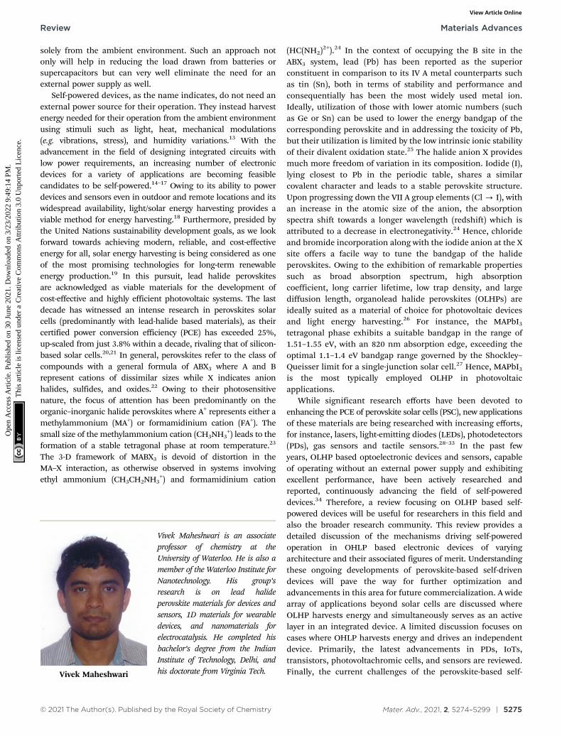
Photovoltaic cells have the limitation of unstable power outputdue to fluctuations in sunlight. Integration of energy storagedevices with solar cells to store energy during sunlight andprovide it under low light conditions can be used to powerwearable electronics.118–126 This provides a stable output powercompared with that of a solar cell alone. Li et al. reported aflexible PSC driven photo-rechargeable lithium-ion capacitor(LIC) for strain sensors.127 It achieved an overall efficiency of8.41% with a high output voltage of 3 V at a discharge currentdensity of 0.1 A g�1. The photovoltaic unit was made by thedeposition of OLHP on an ITO coated PET sheet in Ag/BCP/PCBM/MA1�yFAyPbI3�xClx/NiOx/ITO/PET configuration. A singlecell reached a corresponding PCE of 14.01%, Voc of 1.05 V, short-circuit current density ( Jsc) of 18.71 mA cm�2, and fill factor (FF)of 0.71. Researchers combined four of these PSCs to provide3.95 V with 10.2% efficiency under AM 1.5G solar irradiation.The LIC could be charged to 3 V in 20 min with a charge currentof 1.22 mA. As observed in Fig. 9a–c, the wearable device wasable to monitor finger motion and pulsation continuously andprecisely, without an external power source. In a separate work,Du et al. integrated a flexible graphene-based supercapacitor anda perovskite based solar cell to fabricate a self-powered device.128
The configuration of the perovskite hybrid solar cell (pero-HSC)was ITO/PEDOT:PSS/CH3NH3PbI3�xClx/PC61BM/Al. Under AM1.5G illumination, the pero-HSC exhibited a PCE of 14.13%, aVoc of 0.90 V, a Jsc of 22.59 mA cm�2, and an FF of 0.695. Thesupercapacitor was charged to 0.75 V via the solar cell and
Table 3 Summary of OLHP based flexible self-powered PDs and their associated device characteristics
Device architecture
Self-poweredoperatingprinciple
Operatingwavelength Responsivity
Detectivity(Jones)
Lightswitchingratio
Response speed(rise/fall time) Ref.
Al/MAPbI3/Cu between pair of PET film Triboelectricity 107C/TiO2/MAPbI3-Spiro-OMeTAD/Au Heterojunction 750 nm 16.9 mA W�1 1.10 � 1010 69.1 o200/o200 ms 108C/TiO2/MAPbI3/CuO/Cu2O/Cu Heterojunction 800 nm 562.9 mA W�1 2.15 � 1013 393 o200 ms 109CNY/CH3NH3PbI3/In/Ag Heterojunction 617 nm 10.2 A W�1 1.76 � 1011 45 0.393/0.132 s 110Au/MAPbI3/Au on polyimide Heterojunction 300 nm 2.2 mA W�1 1.76 � 1011 27.2/26.2 ms (2 V) 111PEN/ITO/In2S3/MAPbI3/Spiro-OMeTAD/Ag Heterojunction 720 nm 451 mA W�1 1.1 � 1011 (+0.5 V) o200/o200 ms 112PEN/ITO/SnO2/MAPbI3/Spiro-OMeTAD/Ag Heterojunction 720 nm 473 mA W�1 1.35 � 1013 0.35/0.18 ms 113PET/TETRA-GR/MoS2/MAPbI3/PTAA/Au Heterojunction 720 nm 0.40 A W�1 5.0 � 109 1.63/0.98 ms 114PET/co-GR/MoS2/MAPbI3/PCBM/BCP/Al Heterojunction 700 nm 410 mA W�1 7.99 � 1010 136 110 0.7–0.9/0.4–0.6 s 115Ni/MAPbI3 NWs/Al on polyimide film Schottky Junction 532 nm 0.227 A cm�2 1.36 � 1013 147 61/42 ms 116
Materials Advances Review
Ope
n A
cces
s A
rtic
le. P
ublis
hed
on 3
0 Ju
ne 2
021.
Dow
nloa
ded
on 3
/23/
2022
9:4
9:14
PM
. T
his
artic
le is
lice
nsed
und
er a
Cre
ativ
e C
omm
ons
Attr
ibut
ion
3.0
Unp
orte
d L
icen
ce.
View Article Online
© 2021 The Author(s). Published by the Royal Society of Chemistry Mater. Adv., 2021, 2, 5274–5299 | 5289
discharged from 0.75 to 0 V at 1 A g�1 in about 45 s, showingpromising potential for utilization in self-powered portable andwearable personal devices. Liu et al. designed a photocapacitorwith an overall energy storage efficiency of 70.9% by usingcarbon nanotubes (CNTs) as a bridge between self-poweredorganometal halide PSCs and supercapacitors to improve theoverall performance.129 As observed in Fig. 9d, the CNTs acted asa pathway for holes and electrons resulting in a smaller resistance.Under AM 1.5G simulated sunlight, the PSC of MAPbI3 basedsolar cell achieved a PCE of 2.47%, a Voc of 0.7 V, a Jsc of9.2 mA cm�2, and an FF of 38%. The photocapacitor could becharged to 0.7 V in about 80 s. Following this, it slowly dischargedfrom 0.7 V to 0.3 V, lasting for more than 300 s in dark,representing a more stable output than bare solar cells asillustrated in Fig. 9e.
3. Internet of things (IoT) sensors
Combining photovoltaic cells with the low-power radio frequency(RF) backscatter-based IoT sensors is a new approach toubiquitous sensing for indoor applications.130–134 The perovskitebased photovoltaics can provide the necessary low power for thesesensors enabling their operation for a long time. Kantareddy et al.reported a self-powered perovskite wireless temperature sensorwith a 4 meter communication range.131 Under 1 sun illumina-tion, the PSC with the configuration of FTO/TiO2/(Rb0.01Cs0.05
(FA0.83MA0.17)0.94Pb(I0.83Br0.17)3)/Spiro-OMeTAD/Au exhibited a Voc
of 4.3 V, a Jsc of 3.7 mA cm�2, an FF of 0.6, and a PCE of 10.1%with an active area of 1.06 cm2. This device was able to generateenough power to boot up a radio frequency identification (RFID)device that required 10–45 mW energy. Similarly, Mathews et al.
demonstrated an approach to integrate a wireless temperaturesensor with PSCs acting as an external power source.132 Anintegrated array of three photovoltaic cells, with the configurationof FTO/TiO2/(Rb0.01Cs0.05)(MAxFA1�x)0.94Pb(BrxI1�x)3/Spiro-OMeTAD/Au achieved a Voc, Jsc, and PCE of 2.62 V, 46 mA cm�2 and 13.2%,respectively. The output was 14.5 mW under a light intensity of0.16 mW cm�2 which is enough to power an RFID temperaturesensor. The whole wireless temperature device was operationalfor over 8 h with regular measurements at 1.24 s intervals uponillumination by ambient light.
4. Transistors and photocatalysis
Photovoltaic devices have also been coupled with transistors74,135–139
and electrochemical cells for degradation of organic pollutants,140,141
due to their high Voc (0.9 V to 1.5 V) and power generationcapacity. Jeong et al. reported a MAPbI3 film coupled withPTAA, exhibiting a Jsc and Voc of B21 mA cm�2 and B1.08 V,respectively, with 18.3% PCE.135 The Voc under red-LED couldeffectively gate the MoTe2 field-effect transistors (FET)modulating the drain current (ID), which could turn on/off anOLED pixel (Fig. 10). Chen et al. reported that multi-walledCNTs and a methylamine (CH3NH2) modified perovskiteachieved a PCE of 10.39%.140 It was demonstrated that theCNT-incorporated MAPbI3 perovskite thin film formed asmooth heterojunction structure, which facilitated the separationand transfer of charges. Also, CH3NH2 could self-heal theperovskite surface while maintaining high crystallinity. Thisinhibited the charge recombination and improved the efficiencyof the device. Thus, the CNT/CH3NH2 perovskite exhibited a highJsc value of 22.02 mA cm�2. Combined with the CNT/TiO2
Fig. 9 Schematic of the perovskite photovoltaic cell powered supercapacitor and photocapacitor and their respective responses: (a) scheme of theflexible PSC–LIC–sensor system. (b) Scheme of wearable PSC–LIC–sensor integrated system. (c) The output current response of pulse signal (upperpanel) and finger motion (lower panel) under light illumination. Reprinted from Li et al., flexible perovskite solar cell-driven photo-rechargeable lithium-ion capacitor for self-powered wearable strain sensors, Nano Energy, 60, 247–56.127 Copyright 2019, with permission from Elsevier. (d) Scheme of thephotocapacitor made by organometal halide perovskite and PANI/CNT composites integrated using a CNT bridge. (e) The performance of aphotocapacitor under different illumination conditions. Reproduced from ref. 129 with permission from The Royal Society of Chemistry.
Review Materials Advances
Ope
n A
cces
s A
rtic
le. P
ublis
hed
on 3
0 Ju
ne 2
021.
Dow
nloa
ded
on 3
/23/
2022
9:4
9:14
PM
. T
his
artic
le is
lice
nsed
und
er a
Cre
ativ
e C
omm
ons
Attr
ibut
ion
3.0
Unp
orte
d L
icen
ce.
View Article Online

5290 | Mater. Adv., 2021, 2, 5274–5299 © 2021 The Author(s). Published by the Royal Society of Chemistry
photoanodes and the perovskite PSC (as power source), the systemexhibited an efficient degradation of rhodamine B to almost 100%within 80 min.
5. Photovoltachromic cells
Photovoltachromic cells (PVCCs) can adjust the optical trans-mittance and coloration by their photovoltaic behaviors.142–144
They are of interest for applications in smart windows inbuildings and vehicles to manage daylight admittance. Aphotovoltachromic device integrated with a perovskite basedphotovoltaic cell enables their operation without an externalbias.145–147 Park et al. used a ligand assisted re-precipitationmethod (LARP) to synthesize CH3NH3PbX3 (X = Cl, Br, I, andtheir mixtures) metal halide perovskite nanocrystals (MHPNCs).148 The LARP method used N,N-dimethylformamide(DMF) as a good solvent and toluene as a poor solvent. Whilethe good solvent possessed a slower evaporation rate, thepoor solvent (toluene) induced crystallization leading to theprecipitation of MHP NCs. The authors tuned the energy bandgapand corresponding absorption and emission characteristics of theMAPbX3 MHP NCs by carefully adjusting the ratio of DMF andtoluene. The typical size of the MAPbBr3 MHP NCs was B5 nm.Owing to their reduced size, the MHP NCs exhibited strongluminescence and high quantum yield. The blue, green, and redMHP NCs were utilized to fabricate a panchromatic photodetectorcell that showed a full-colored emission spectrum spanning435–631 nm (Fig. 11a and b). The effective panchromatic photonharvesting was attributed to the individual absorption of blue,green, and red light by the corresponding MHP NCs and the
independent transfer of the photogenerated electrons into themesoporous TiO2 electrode. Cannavale et al. were amongst thefirst to report a self-powered photovoltachromic device integratedusing a perovskite and an electrochromic supercapacitor (ECS).149
Here, the ECS included a layer of WO3 which could store chargesand change the color at the same time owing to the change of thechemical state in W. As reported, WO3 is transparent, and WO3
�
is colored.146 As seen in Fig. 11c–e, once the device was exposed tosolar illumination, the perovskite was capable of generatingenough power to activate the coloring of WO3 without requiringany external bias. Therefore, the device processed a chromictransition from semi-transparent to dark blue when irradiatedby solar light. The perovskite layer presented a Voc of 0.68 V, a Jsc
of 12.5 mA cm�2, an FF of 0.63, and a PCE of 5.5%. As for thePVCC, it showed average visible transmittance (AVT) of 15.9%.Illuminated at AM 1.5 sunlight, the cell’s AVT changed to 5.5%.Similarly, Zhou et al. vertically stacked PSC with MoO3/Au/MoO3
(MAM), all transparent electrode and WO3 ECS to producea photovoltachromic supercapacitor (PVCSs) which can storethe electrochemical energy accompanied by color change.150
This design not only provided a seamless integration of energyharvesting and storage device but also improved photostability.The photocharging process changed the color of the PVCSs fromtransparent to dark blue. During the fully charged state, thecolored PVCSs blocked off most of the light automatically turningthe PSC into the low power operating state and preventing the cellfrom long-time exposure, thereby prolonging the device lifetime.The transparent electrodes facilitated the possibility of PSC to beilluminated from both sides. In the co-cathode structure, the FTOglass served as the co-cathode for both PSC and ECS. While for theco-anode structure, the MAM electrode served as a co-anode for
Fig. 10 Perovskite solar cell powered FET and the corresponding photosensitive response: (a) photo image and optical microscope image (inset) ofn-MoTe2 FET. (b) Scheme of the MAPbI3-based perovskite PV cells. (c) Current density–voltage curve of the PV cell measured under 1 sun illumination.(d) Cross-section scheme of the packaged device. Light intensity-dependent (e) Vout and (f) Iout of the packaged device under periodic red LEDillumination, respectively. Reprinted from Jeong et al., Integrated advantages from perovskite photovoltaic cell and 2D MoTe2 transistor towards self-power energy harvesting and photosensing, Nano Energy, 63, 103833.135 Copyright 2019, with permission from Elsevier.
Materials Advances Review
Ope
n A
cces
s A
rtic
le. P
ublis
hed
on 3
0 Ju
ne 2
021.
Dow
nloa
ded
on 3
/23/
2022
9:4
9:14
PM
. T
his
artic
le is
lice
nsed
und
er a
Cre
ativ
e C
omm
ons
Attr
ibut
ion
3.0
Unp
orte
d L
icen
ce.
View Article Online

© 2021 The Author(s). Published by the Royal Society of Chemistry Mater. Adv., 2021, 2, 5274–5299 | 5291
both PSC and ECS. When PSC was in the co-anode mode (or theco-cathode), PVCS with the light illumination demonstrated a Voc
of 0.983 V (or 1.000 V), a Jsc of 12.46 mA cm�2 (or 18.17 mA cm�2),an FF of 0.654% (or 0.654%), and a PCE of 8.25% (or 11.89%).With the color change, the PCEs of the co-anode and co-cathodePVCSs decreased to 3.73% and 2.26%, respectively.
6. Pressure sensors
Flexible pressure sensors have numerous applications in areassuch as artificial electronic skins,145,151,152 health monitoringdevices,153–156 soft robotics,157–159 and wearable technology.160–165
It also improves the seamless interfacing of such devices with theenvironment to act as a medium for information collection todrive robotics and human–artificial intelligence interactions.166
The OLHP based self-powered pressure sensors and the corres-ponding device characteristics are listed in Table 4.
6.1 Mechanoluminescent device
Shohag et al. reported a flexible pressure sensor by integrating amechanoluminescent device with a B500 nm thick organometalhalide perovskite.162 In this work, the authors attempted atreducing the defect density of the perovskite by incorporatingbromine which led to reduced trapping of charge carriers at thegrain boundaries and hence, enhanced the efficiency. An appliedmechanical force led the ZnS:Cu crystals to emit mechano-luminescence at B543 nm, which could be then absorbed bythe ultrathin layer of perovskite (MAPb(Br0.1I0.9)3) to generate aphotocurrent. The photocurrent generated in the perovskitelayer increased with the increase in the intensity of light emittedfrom the ZnS:Cu layer, in direct proportion to the appliedpressure. The sensor was able to detect pressure from 11 kPa
to 460 kPa with a sensitivity of 0.095 kPa�1. The sensor alsoexhibited a steady response over 1000 bending cycles, which ispromising for monitoring health signals.
6.2 Piezoelectric effect assisted sensing
MAPbI3 is a semi-conductor and poly(vinylidene fluoride)(PVDF) is a piezoelectric material. Researchers have combinedthese two materials to develop self-powered pressure sensorsbased on their combined properties. For example, Jella et al.constructed a flexible and wearable piezoelectric generator(PEG) by using the MAPbI3 perovskite and PVDF as a piezo-electric flexible polymer matrix.167 The strong dipolar inter-actions between MA+ and the fluorine groups of the PVDF (–CF2–)result in a high dielectric constant, low leakage current, and highstability. As observed in Fig. 12, under an applied force, macro-dipoles are formed resulting in charge accumulation at theMAPbI3–PVDF interface with opposite polarity, so the chargedensity of the electrode decreases generating a positive signalwhile the releasing process produced a negative signal. Thedevice showed a Voc of 45.6 V and a Jsc of 4.6 mA cm�2 withhigh mechanical stability. The generated output can powercommercial LEDs under a 50 N applied force by finger tapping.Sultana et al. produced a flexible self-powered perovskite basedpiezoelectric nanogenerator (P-PNG) by electrospinning PVDFnanofibers and MAPbI3.158 The mechanical vibration led to achange of output power density with a piezoelectric coefficient ofB19.7 pC N�1 which shows appreciable potential for a pressuresensor. The Voc increased with the frequency of applied stress asmore charges are generated. As illustrated in Fig. 13a–d, at 4 Hz,the Voc reached a maximum of 220 mV while gradually decreasingto 100 mV at 15 Hz. The authors also measured the stability of thedevice, which showed a stable response for 60 000 cycles at 4 Hz
Fig. 11 Perovskite based panchromatic photodetectors and photovoltachromic devices: (a) scheme of the good–poor solvent enriched preparationprocess of MMH NC films by spin-coating. (b) Normalized PL spectra of blue, green, and red MHP NC-films. Reprinted from Park et al., Synthesis of post-processable metal halide perovskite nanocrystals via the modified ligand-assisted re-precipitation method and their applications in self-poweredpanchromatic photodetectors, J. Ind. Eng. Chem., 92, 167–173.148 Copyright 2020, with permission from Elsevier. (c) Scheme of axonometric view of thephotovoltachromic device. The optical image of the device under (d) bleached and (e) colored conditions. Reproduced from ref. 149 with permissionfrom The Royal Society of Chemistry.
Review Materials Advances
Ope
n A
cces
s A
rtic
le. P
ublis
hed
on 3
0 Ju
ne 2
021.
Dow
nloa
ded
on 3
/23/
2022
9:4
9:14
PM
. T
his
artic
le is
lice
nsed
und
er a
Cre
ativ
e C
omm
ons
Attr
ibut
ion
3.0
Unp
orte
d L
icen
ce.
View Article Online

5292 | Mater. Adv., 2021, 2, 5274–5299 © 2021 The Author(s). Published by the Royal Society of Chemistry
with a 7.5 N applied force. Sultana et al. also developed acantilever structured self-powered vibration sensor (SPVS) forlow-frequency vibration detection by combining MAPbBr3 andPVDF.168 Based on the intrinsic properties of the PEG, the largerdisplacement of the tip increased the strain applied on the filmresulting in an output voltage. Thus, the output voltage of theSPVS was able to sense the frequency and amplitude of vibration
with a sensitivity of 0.02 V mm�1. This device showed thepossibility of detecting the vibrations from railway or constructionequipment without an external bias. Recently, Khan et al.presented a flexible and highly porous FAPbBr2I–PVDF P-PNGassembly.159 The high strain of the self-assembled highly orderedpolymer scaffold and enhanced relative permittivity of theperovskite led to a 5 fold improvement in the strain-induced
Table 4 Summary of OLHP based pressure-sensitive devices and their associated parameters
Device type Device architecturePeak outputvoltage/Voc
Peak outputcurrent/Jsc
Sensitivity/minimumpressure Application and features Ref.
Mechanoluminescent ZnS:Cu-PDMS/PET/ITO/SnO2/CH3NH3Pb(Br0.1I0.9)3/Spiro-OMeTAD/Au
0.095 kPa�1 Self-powered luminescent device,sensitivity range: 11 kPa to460 kPa
162
Piezoelectric effectassisted sensor
PI-Ti/Au/PDMS/MAPbI3–PVDF/ITO-PET
45.6 V 4.7 mA cm�2 PEG could power commercialLEDs under an applied force of50 N, a high dielectric constant ofB56 at 1 kHz, and remanentpolarization of 0.83 mC cm�2
167
Ni/PVDF–MAPbI3 nanofibermat/Cu
B220 mV 18.2 pA Self-powered pyroelectrictemperature sensor, pyroelectriccoefficient of B44 pC m�2 K�1
with a response and reset times ofB1.14 and B1.25 s, respectively
158
Ag/MAPbBr3–PVDF/Ag B0.25 V 0.02 V mm�1 Self-powered vibration sensor 168Polyester/Cu/FAPbBr2I–PVDF/Cu/polyester
85 V B30 mA Self-powered integrated wirelesselectronic node, peak outputpower density of 10 mW cm�2
159
Glass/3 at% Al doped ZnO(AZO)/Au/AZO/MAPbI3/SiO2/AZO/Au/AZO
125.6 � 2.4 mVand �30.2 � 8.2 mV
0.8 nA 8.34 mV kPa�1
and0.02 nA kPa�1
Self-powered light and pressuresensor, sensitivity range: 5 to40 kPa
169
Response speed: 0.066/0.320 sZnO nanosheets on Au/MAPbI3/Au
0.57 kPa�1 Self-powered tactile sensor, sensi-tivity range: 0.5 kPa to 76 kPa;
166
ITO/ZnO nanosheets on Au/PS–MAPbI3/Au
B325 mV B0.12 mA cm�2 19.77 kPa�1 Self-powered tactile sensor,sensitivity range: 4 Pa to 450 kPa
170
Fig. 12 Schematic of piezoelectric based origin of self-powered operation in perovskite–polymer composite and the generated response: (a) scheme ofthe MAPbI3–PVDF composite-based PEG working mechanism. (b) The Voc and Jsc response of MAPbI3–PVDF PEG under an applied force of 50 N.(c) Photo images of an instant turn on 10 green LEDs by rectified electric power from the harvesting device. Insets present the scheme of the circuit andlighting of LEDs in dark. Reprinted from Jella et al., Enhanced output performance of a flexible piezoelectric energy harvester based on stable MAPbI3–PVDF composite films, Nano Energy, 53, 46–56.167 Copyright 2018, with permission from Elsevier.
Materials Advances Review
Ope
n A
cces
s A
rtic
le. P
ublis
hed
on 3
0 Ju
ne 2
021.
Dow
nloa
ded
on 3
/23/
2022
9:4
9:14
PM
. T
his
artic
le is
lice
nsed
und
er a
Cre
ativ
e C
omm
ons
Attr
ibut
ion
3.0
Unp
orte
d L
icen
ce.
View Article Online

© 2021 The Author(s). Published by the Royal Society of Chemistry Mater. Adv., 2021, 2, 5274–5299 | 5293
piezo potential (B85 V) and 15 times higher current (B30 mA) inthe perovskite-polymer composite P-PNG relative to those of thepristine PVDF PNG, at an applied load of 138 g. Utilizing theP-PNG, the authors further demonstrated a self-powered universalwireless electronics node (SIWEN) capable of communicatingremotely with personal electronics. Energy harvesting from areal-life scenario such as automobile vibrations and biomechanicalmotion was also demonstrated. Eom et al. used the CVD method tofabricate a 500 nm thin film of MAPbI3.169 The film was stable for amonth under ambient conditions. Owning to an intrinsic piezo-electric property of MAPbI3, the device showed sensitivity to bothpressure and light. The MAPbI3 film had a linear sensitivity to apressure of 8.34 mV kPa�1 and 0.02 nA kPa�1 within a pressurerange of 40 kPa, generated by finger touch. There was a time delayof 0.072 and 0.087 s in detection on applying and removing thepressure. The delay was attributed to the domain switching due toapplied pressure on the film. In an interesting work, Saraf et al.combined a layer of ZnO nanosheets as a pressure-sensitiveelectron extraction layer on the MAPbI3 film (Fig. 13e and f).166
A small external bias was applied for few minutes to the MAPbI3
film to induce polarization effects capable of generatingspontaneous voltage and current response upon light illuminationonce the external bias was removed. The pressure applied on thetop ZnO layer increased the interfacing area between the MAPbI3
film and the ZnO layer, leading to a higher collection of electrons.This action increased the value of Jsc (or Voc) in proportion to the
applied pressure, as shown in Fig. 13f. The sensor exhibited a linearresponse from 0.5 kPa to 76 kPa with a sensitivity of 0.57 kPa�1.After 100 load cycles, the device had a stable current generationdensity of 0.2 mA cm�2. This tactile sensor demonstrated a lowenergy cost as it could operate over 72 h after poling for 5 min at1.5 V mm�1. To further improve the stability of the sensor, Sarafet al. used hydrophobic PS with MAPbI3. The resultant polymer–perovskite hybrid device displayed stability under ambientconditions for over 1000 h.170 Also, the inclusion of the polymerled to a softer film with a lower modulus which dissipated the forcestimuli leading to a wide operating range. Once poled, the film wasfunctional as a self-driven light-powered tactile sensor for 120 hand could be re-poled for continued operational performance.The light-powered tactile sensor fabricated by the assembly of1 wt% PS–MAPbI3 film and ZnO exhibited a wide operating rangefrom 4 Pa up to 333 kPa with linear response and a sensitivity of19.77 kPa�1.
7. Gas sensors
Today, there is an increasing need for portable self-powered gassensing devices to monitor personal health, toxic gas release,and safety in public space.141,154,171–176 Chen et al. synthesizeda self-powered nitrogen dioxide (NO2) sensing device based onFA0.80MA0.15Cs0.05PbI2.55Br0.45 (FMCPIB) perovskites.141 The authors
Fig. 13 Device schematic, images, and the electro-optical response of P-PNG and perovskite based self-powered tactile sensor: (a) PVDF–MAPInanofiber mat sandwiched between two electrodes. (b) Optical image of the flexible P-PNG wrapped on a pen. (c) Optical image of bent P-PNG. (d)Output voltage response of P-PNG of applied force under different frequencies. Reprinted with permission from Sultana et al., ACS Appl. Mater.Interfaces, 11, 27279–27287.158 Copyright r 2019 American Chemical Society. (e) Schematic of the solar-powered tactile sensor. Inset shows SEM imageof ZnO sheets on the perovskite layer. (f) The response of Jsc under the stepped applied pressure under 1 sun illumination. Reproduced with permissionfrom Saraf et al., Adv. Mater., 30, 1705778.166 r 2018 WILEY-VCH Verlag GmbH & Co. KGaA, Weinheim.
Review Materials Advances
Ope
n A
cces
s A
rtic
le. P
ublis
hed
on 3
0 Ju
ne 2
021.
Dow
nloa
ded
on 3
/23/
2022
9:4
9:14
PM
. T
his
artic
le is
lice
nsed
und
er a
Cre
ativ
e C
omm
ons
Attr
ibut
ion
3.0
Unp
orte
d L
icen
ce.
View Article Online

5294 | Mater. Adv., 2021, 2, 5274–5299 © 2021 The Author(s). Published by the Royal Society of Chemistry
fabricated a photovoltaic cell with the vertical configuration of FTO/TiO2/FMCPIB/carbon. The authors believed that NO2 can undergointeraction with the amine cation of FMCPIB. This interaction wasattributed to reducing the defects in the perovskite film whichdecreases the charge recombination and hence increasing thedensity of free charge carriers. Fig. 14 represents the deviceperformance of NO2 detection at room temperature under O2 richconditions. A linear relationship up to 8 ppm with a 0.2 ppmdetection limit under ambient conditions was observed. A higherNO2 concentration led to a higher output current due to theinteraction between NO2 and FMCPIB. Owing to the functionalityof the FMCPIB to act as a gas sensor, light harvester, and capacitiveenergy storage material (due to mobile ions), the self-powereddevice stayed in operation for 1.7 h in dark without requiring anexternal power supply. The measured response and recovery timeswere 17 s and 126 s, respectively. Such gas sensing ability bankingon the inherent material properties of OLHP may pave new ways tomonitor environmental safety using self-powered sensors.
Challenges and future prospects
Continuous research has led to significant advances in theOLHP based self-powered devices both in terms of theirperformance and expanding their applications. Various devicesbesides solar cells, such as PDs, supercapacitors, and TENGs,
are being fabricated primarily using OLHP as a photosensitivelayer. The development of self-powered electroluminescentdevices using OLHP can also benefit from an increasedresearch focus. The challenge lies in the typical high voltagerequirement for generating appreciable luminescence. The useof polarization effects in OLHP is a potential route for suchdevices, with the research required to understand and enhancethese characteristics for the generation of greater energy andelectric potential. The inherent stability issue of the perovskitematerial is a major challenge that persists due to the inherentstructure of the material (high ion mobilities) and its sensitivityto multiple external factors (such as humidity, oxygen,illumination, and temperature). Strategies such as interfacialengineering, additive integration, doping, and encapsulationare being widely adopted to reduce perovskite degradation.A significant scope also exists for the improvement of theinherent perovskite structure and composition. These combinedefforts result in improving the lifetime of the OLHP baseddevices and should continue to progress them towardscommercial viability. With the concerns of toxicity surroundinglead, there are ongoing efforts of substituting it with otherdivalent ions such as Sn, Ge, Bi, and Sb, but the resultingreduction in performance needs to be addressed in order todevelop lead-free perovskites.177,178
At a macroscale, as it stands, the majority of OLHP basedself-powered devices and sensors are rigid. Although, in the last
Fig. 14 Design and self-powered chemical response of the FMCPIB-based gas sensor at room temperature: (a) scheme of the FMCPIB-based gassensor. (b) The current response of the FMCPIB devices with the injection of 8 ppm NO2. (c) The sensor response for six different gases. (d) The sensorresponse as a function of the NO2 concentration in the self-powered mode. Reproduced with permission from Chen et al., Adv. Opt. Mater., 8,1901863.141 r 2020 WILEY-VCH Verlag GmbH & Co. KGaA, Weinheim.
Materials Advances Review
Ope
n A
cces
s A
rtic
le. P
ublis
hed
on 3
0 Ju
ne 2
021.
Dow
nloa
ded
on 3
/23/
2022
9:4
9:14
PM
. T
his
artic
le is
lice
nsed
und
er a
Cre
ativ
e C
omm
ons
Attr
ibut
ion
3.0
Unp
orte
d L
icen
ce.
View Article Online
© 2021 The Author(s). Published by the Royal Society of Chemistry Mater. Adv., 2021, 2, 5274–5299 | 5295
few years flexible transducers are being researched and reportedwith greater intensity, they experience performance degradationduring long-term operations. Most wearable and portable electronicdevices and sensors mandate the ability to be stretched andbent over a couple of thousand cycles without incurringsignificant decay in output over time. Alternatives for 3D OLHPsuch as 2D, 1D, and 0D OLHP may offer enhanced flexibility andmight provide viable options.179–182 Equally critical is the need fordeveloping appropriate substrates and electrodes for long-termdevice operation while ensuring wearability comfort. Furthermore,it is worth considering that almost all OLHP self-powered portableand wearable devices are tested at 1 sun. However, the indoorperformance of these devices with limited illumination is rarelyreported. Therefore, developing standard protocols for testingdevices under such limited light conditions need to be developedas this will allow a more accurate comparison of devices.
Although low levels of the output signals and non-continuous operation seem to impede the overall capability ofthe OLHP based self-driven devices and sensors, several othermajor factors contribute to hinder the commercial viability ofsuch perovskite-based transducers. Currently, there is a lack ofa standardized large-scale manufacturing process that couldensure performance consistency amongst batches of thesame device. Besides, there is limited research available overperformance–cost analysis specific to the OLHP self-powereddevices that could drive them from a lab prototype to acommercial finished product. OLHP is considered a low-costmaterial compared to other semiconductors (such as Si andorganic compounds); however, a more detailed cost analysisis required for the quantification of its cost advantage (includ-ing Pb recycling needs). Techniques such as printing need to bepromoted to drive up large scale cost-effective production of theOLHP based self-powered devices. The use of advanced micro-fabrication and nanofabrication techniques can further expandthe integration of other flexible electronic, photonic, andoptoelectronic devices with OLHP as an energy harvester.
In summary, significant advancements have been made inOLHP based self-powered applications, but still there are criticalchallenges that need to be addressed before they can be consideredcommercially viable products. The rapid development of materialsscience, processing, and manufacturing technology can enable theprogress of the OLHP based self-powered system in our day-to-daylife at a rapid pace and the commercialization of OLHP basedphotovoltaic cells provides important lessons for this road map.
Author contributions
Avi Mathur: conceptualization, investigation, and writing –original draft. Hua Fan: investigation and writing – originaldraft. Vivek Maheshwari: conceptualization, funding acquisi-tion, resources, writing – review & editing, and supervision.
Conflicts of interest
There are no conflicts to declare.
Acknowledgements
This work was supported by the University of Waterloo, GeraldSchwartz and Heather Reisman Foundation, Canada Founda-tion for Innovation, Early Researcher Award from the Ministryof Research and Innovation and Science, Ontario, and NSERCCanada.
References
1 L. Atzori, A. Iera and G. Morabito, Comput. Networks, 2010,54, 2787–2805.
2 F. Xia, L. T. Yang, L. Wang and A. Vinel, Int. J. Commun.Syst., 2012, 25, 1101.
3 Y. Yuehong, Y. Zeng, X. Chen and Y. Fan, J. Ind. Inf. Integr.,2016, 1, 3–13.
4 C. Xu, Y. Song, M. Han and H. Zhang, Microsyst. Nanoeng.,2021, 7, 1–14.
5 M. J. Cima, Nat. Biotechnol., 2014, 32, 642–643.6 N. Xu, S. Rangwala, K. K. Chintalapudi, D. Ganesan,
A. Broad, R. Govindan and D. Estrin, A wireless sensornetwork for structural monitoring, 2004.
7 J. Kim, R. A. Swartz, J. P. Lynch, J.-J. Lee and C.-G. Lee,Smart Struct. Syst., 2010, 6, 505–524.
8 F. Zhang, X. Liu, S. A. Hackworth, R. J. Sclabassi andM. Sun, In vitro and in vivo studies on wireless poweringof medical sensors and implantable devices, IEEE, 2009.
9 D. Fitzpatrick, Implantable electronic medical devices, Else-vier, 2014.
10 F. Larsson, P. Andersson, P. Blomqvist and B.-E.Mellander, Sci. Rep., 2017, 7, 1–13.
11 J. Sun, J. Li, T. Zhou, K. Yang, S. Wei, N. Tang, N. Dang,H. Li, X. Qiu and L. Chen, Nano Energy, 2016, 27, 313–319.
12 R. W. Keyes, IBM J. Res. Dev., 1988, 32, 84–88.13 P. Glynne-Jones and N. White, Sens. Rev., 2001, 21,
91–98.14 Q. Zheng, Q. Tang, Z. L. Wang and Z. Li, Nat. Rev. Cardiol.,
2020, 1–15.15 K. M. Reilly, M. T. Birner and N. G. Johnson, Measuring air
quality using wireless self-powered devices, IEEE, 2015.16 Z. Liu, B. Cho, T. Ouyang and B. Feldman, Anal. Chem.,
2012, 84, 3403–3409.17 F.-R. Fan, L. Lin, G. Zhu, W. Wu, R. Zhang and Z. L. Wang,
Nano Lett., 2012, 12, 3109–3114.18 J. Zhao, R. Ghannam, K. O. Htet, Y. Liu, M. K. Law,
V. A. Roy, B. Michel, M. A. Imran and H. Heidari, Adv.Healthcare Mater., 2020, 9, 2000779.
19 J. Twidell and T. Weir, Renewable energy resources, Routle-dge, 2015.
20 A. Kojima, K. Teshima, Y. Shirai and T. Miyasaka, J. Am.Chem. Soc., 2009, 131, 6050–6051.
21 National Renewable Energy Laboratory – Best research-cellefficiencies chart, https://www.nrel.gov/pv/cell-efficiency.html, accessed April, 2021.
22 K. P. Ong, T. W. Goh, Q. Xu and A. Huan, J. Phys. Chem. A,2015, 119, 11033–11038.
Review Materials Advances
Ope
n A
cces
s A
rtic
le. P
ublis
hed
on 3
0 Ju
ne 2
021.
Dow
nloa
ded
on 3
/23/
2022
9:4
9:14
PM
. T
his
artic
le is
lice
nsed
und
er a
Cre
ativ
e C
omm
ons
Attr
ibut
ion
3.0
Unp
orte
d L
icen
ce.
View Article Online

5296 | Mater. Adv., 2021, 2, 5274–5299 © 2021 The Author(s). Published by the Royal Society of Chemistry
23 C. Quarti, E. Mosconi, J. M. Ball, V. D’Innocenzo, C. Tao,S. Pathak, H. J. Snaith, A. Petrozza and F. De Angelis,Energy Environ. Sci., 2016, 9, 155–163.
24 Q. Chen, N. De Marco, Y. M. Yang, T.-B. Song, C.-C. Chen,H. Zhao, Z. Hong, H. Zhou and Y. Yang, Nano Today, 2015,10, 355–396.
25 F. Hao, C. C. Stoumpos, D. H. Cao, R. P. Chang andM. G. Kanatzidis, Nat. Photonics, 2014, 8, 489.
26 L. Chouhan, S. Ghimire, C. Subrahmanyam, T. Miyasakaand V. Biju, Chem. Soc. Rev., 2020, 49, 2869–2885.
27 S. Pang, H. Hu, J. Zhang, S. Lv, Y. Yu, F. Wei, T. Qin, H. Xu,Z. Liu and G. Cui, Chem. Mater., 2014, 26, 1485–1491.
28 J. Song, J. Li, X. Li, L. Xu, Y. Dong and H. Zeng, Adv. Mater.,2015, 27, 7162–7167.
29 Q. Shan, J. Song, Y. Zou, J. Li, L. Xu, J. Xue, Y. Dong,B. Han, J. Chen and H. Zeng, Small, 2017, 13, 1701770.
30 L. Xu, J. Li, B. Cai, J. Song, F. Zhang, T. Fang and H. Zeng,Nat. Commun., 2020, 11, 1–12.
31 J. Chen, J. Wang, X. Xu, J. Li, J. Song, S. Lan, S. Liu, B. Cai,B. Han and J. T. Precht, Nat. Photonics, 2021, 15, 238–244.
32 J. Sun, J. Wu, X. Tong, F. Lin, Y. Wang and Z. M. Wang, Adv.Sci., 2018, 5, 1700780.
33 R. Saraf and V. Maheshwari, Functional Tactile Sensors,Elsevier, 2021, pp. 141–158.
34 X. Zhang, X. Dong, S. Wang, H. Liu, W. Hu and X. Li, Chem.Eng. J., 2021, 404, 125957.
35 F. P. G. de Arquer, A. Armin, P. Meredith and E. H. Sargent,Nat. Rev. Mater., 2017, 2, 1–17.
36 Y. Xie, B. Zhang, S. Wang, D. Wang, A. Wang, Z. Wang,H. Yu, H. Zhang, Y. Chen and M. Zhao, Adv. Mater., 2017,29, 1605972.
37 E. Dupont, M. Byloos, M. Gao, M. Buchanan, C.-Y. Song,Z. Wasilewski and H. Liu, IEEE Photonics Technol. Lett.,2002, 14, 182–184.
38 C. Chen, K. Choi, W. Chang and D. Tsui, Appl. Phys. Lett.,1998, 72, 7–9.
39 S. Donati, Photodetectors: devices, circuits and applications,John Wiley & Sons, 2021.
40 G. Konstantatos, Nat. Commun., 2018, 9, 5266.41 X. Feng, M. Tan, M. Li, H. Wei and B. Yang, Nano Lett.,
2021, 21, 1500–1507.42 Y. Liu, Y. Zhang, X. Zhu, Z. Yang, W. Ke, J. Feng, X. Ren, K. Zhao,
M. Liu and M. G. Kanatzidis, Sci. Adv., 2021, 7, eabc8844.43 T. M. H. Nguyen, S. Kim and C. W. Bark, J. Mater. Chem. A,
2021, 9, 1269–1276.44 C. Perumal Veeramalai, S. Feng, X. Zhang, S. V. N. Pammi,
V. Pecunia and C. Li, Photonics Res., 2021, 9, 968–991.45 L. Dou, Y. M. Yang, J. You, Z. Hong, W.-H. Chang, G. Li and
Y. Yang, Nat. Commun., 2014, 5, 1–6.46 M. Zhang, M. Ye, W. Wang, C. Ma, S. Wang, Q. Liu, T. Lian,
J. Huang and Z. Lin, Adv. Mater., 2020, 32, 2000999.47 B. Wang, M. Zhang, X. Cui, Z. Wang, M. Rager, Y. Yang,
Z. Zou, Z. L. Wang and Z. Lin, Angew. Chem., 2020, 132,1628–1635.
48 M. Zhang, X. Cui, Y. Wang, B. Wang, M. Ye, W. Wang,C. Ma and Z. Lin, Nano Energy, 2020, 71, 104620.
49 Z. Wang, R. Yu, C. Pan, Z. Li, J. Yang, F. Yi and Z. L. Wang,Nat. Commun., 2015, 6, 1–7.
50 J. Yu, X. Chen, Y. Wang, H. Zhou, M. Xue, Y. Xu, Z. Li,C. Ye, J. Zhang and P. A. Van Aken, J. Mater. Chem. C, 2016,4, 7302–7308.
51 Y. Zhu, Z. Song, H. Zhou, D. Wu, R. Lu, R. Wang andH. Wang, Appl. Surf. Sci., 2018, 448, 23–29.
52 H. Zhou, L. Yang, P. Gui, C. R. Grice, Z. Song, H. Wang andG. Fang, Sol. Energy Mater. Sol. Cells, 2019, 193, 246–252.
53 X. Yang, Y. Zhu, H. Zhou, Z. Song, R. Liu, L. Shen andH. Wang, Appl. Surf. Sci., 2020, 504, 144468.
54 Z. Liu, X. Liu, B. Sun, X. Tan, H. Ye, J. Zhou, Z. Tang, T. Shiand G. Liao, Adv. Mater. Technol., 2020, 5, 2000260.
55 H. Zhou, J. Mei, M. Xue, Z. Song and H. Wang, J. Phys.Chem. C, 2017, 121, 21541–21545.
56 J. Ghosh, G. Natu and P. Giri, Org. Electron., 2019, 71,175–184.
57 D. H. Shin, S. H. Shin, S. G. Lee, S. Kim and S.-H. Choi, ACSSustainable Chem. Eng., 2019, 7, 19961–19968.
58 Y. Cheng, Z. Shi, S. Yin, Y. Li, S. Li, W. Liang, D. Wu,Y. Tian and X. Li, Sol. Energy Mater. Sol. Cells, 2020,204, 110230.
59 L. Shen, Y. Fang, D. Wang, Y. Bai, Y. Deng, M. Wang, Y. Luand J. Huang, Adv. Mater., 2016, 28, 10794–10800.
60 Q. Shan, C. Wei, Y. Jiang, J. Song, Y. Zou, L. Xu, T. Fang,T. Wang, Y. Dong and J. Liu, Light: Sci. Appl., 2020, 9, 1–9.
61 C. Lan, H. Zou, L. Wang, M. Zhang, S. Pan, Y. Ma, Y. Qiu,Z. L. Wang and Z. Lin, Adv. Mater., 2020, 32, 2005481.
62 Z. Li, H. Li, K. Jiang, D. Ding, J. Li, C. Ma, S. Jiang, Y. Wang,T. D. Anthopoulos and Y. Shi, ACS Appl. Mater. Interfaces,2019, 11, 40204–40213.
63 T. Pang, R. Jia, Y. Wang, K. Sun, Z. Hu, Y. Zhu, S. Luan andY. Zhang, J. Mater. Chem. C, 2019, 7, 609–616.
64 L. Ren, M. Wang, M. Li, S. Wang, S. Wang, Y. Zhao,M. A. Iqbal and K. Jin, Opt. Mater., 2020, 100, 109687.
65 K. Pandey, M. Chauhan, V. Bhatt, B. Tripathi, P. Yadav andM. Kumar, RSC Adv., 2016, 6, 105076–105080.
66 J. Li, S. Yuan, G. Tang, G. Li, D. Liu, J. Li, X. Hu, Y. Liu, J. Liand Z. Yang, ACS Appl. Mater. Interfaces, 2017, 9,42779–42787.
67 Q. Zeng and Z. Liu, Adv. Electron. Mater., 2018, 4, 1700335.68 M. Pandey, R. Soni, A. Mathur, A. Singh, A. K. Singh,
S. Raghavan and U. Chandni, Phys. Rev. Appl., 2019,12, 064032.
69 D. Sarkar, W. Liu, X. Xie, A. C. Anselmo, S. Mitragotri andK. Banerjee, ACS Nano, 2014, 8, 3992–4003.
70 N. Rohaizad, C. C. Mayorga-Martinez, Z. K. Sofer andM. Pumera, ACS Appl. Mater. Interfaces, 2017, 9, 40697–40706.
71 S. Barua, H. S. Dutta, S. Gogoi, R. Devi and R. Khan, ACSAppl. Nano Mater., 2017, 1, 2–25.
72 J. H. Lee, J. Y. Park, E. B. Cho, T. Y. Kim, S. A. Han,T. H. Kim, Y. Liu, S. K. Kim, C. J. Roh and H. J. Yoon, Adv.Mater., 2017, 29, 1606667.
73 A. Di Bartolomeo, A. Grillo, F. Urban, L. Iemmo,F. Giubileo, G. Luongo, G. Amato, L. Croin, L. Sun andS. J. Liang, Adv. Funct. Mater., 2018, 28, 1800657.
Materials Advances Review
Ope
n A
cces
s A
rtic
le. P
ublis
hed
on 3
0 Ju
ne 2
021.
Dow
nloa
ded
on 3
/23/
2022
9:4
9:14
PM
. T
his
artic
le is
lice
nsed
und
er a
Cre
ativ
e C
omm
ons
Attr
ibut
ion
3.0
Unp
orte
d L
icen
ce.
View Article Online

© 2021 The Author(s). Published by the Royal Society of Chemistry Mater. Adv., 2021, 2, 5274–5299 | 5297
74 F. Bai, J. Qi, F. Li, Y. Fang, W. Han, H. Wu and Y. Zhang,Adv. Mater. Interfaces, 2018, 5, 1701275.
75 L. H. Zeng, Q. M. Chen, Z. X. Zhang, D. Wu, H. Yuan,Y. Y. Li, W. Qarony, S. P. Lau, L. B. Luo and Y. H. Tsang,Adv. Sci., 2019, 6, 1901134.
76 Y. Kutes, L. Ye, Y. Zhou, S. Pang, B. D. Huey andN. P. Padture, J. Phys. Chem. Lett., 2014, 5, 3335–3339.
77 J. M. Frost, K. T. Butler, F. Brivio, C. H. Hendon, M. VanSchilfgaarde and A. Walsh, Nano Lett., 2014, 14, 2584–2590.
78 L. M. Garten, D. T. Moore, S. U. Nanayakkara, S. Dwaraknath,P. Schulz, J. Wands, A. Rockett, B. Newell, K. A. Persson andS. Trolier-McKinstry, Sci. Adv., 2019, 5, eaas9311.
79 A. Gomez, Q. Wang, A. R. Goni, M. Campoy-Quiles andA. Abate, Energy Environ. Sci., 2019, 12, 2537–2547.
80 Z. Fan, J. Xiao, K. Sun, L. Chen, Y. Hu, J. Ouyang, K. P. Ong,K. Zeng and J. Wang, J. Phys. Chem. Lett., 2015, 6, 1155–1161.
81 M. N. F. Hoque, M. Yang, Z. Li, N. Islam, X. Pan, K. Zhuand Z. Fan, ACS Energy Lett., 2016, 1, 142–149.
82 R. Saraf and V. Maheshwari, ACS Appl. Mater. Interfaces,2018, 10, 21066–21072.
83 A. Mathur, A. Li and V. Maheshwari, J. Phys. Chem. Lett.,2021, 12, 1481–1489.
84 F. Cao, W. Tian, M. Wang and L. Li, ACS Photonics, 2018, 5,3731–3738.
85 F. Cao, W. Tian, L. Meng, M. Wang and L. Li, Adv. Funct.Mater., 2019, 29, 1808415.
86 F. Cao, W. Tian, M. Wang, H. Cao and L. Li, Adv. Funct.Mater., 2019, 29, 1901280.
87 L. Su, Z. X. Zhao, H. Y. Li, J. Yuan, Z. L. Wang, G. Z. Caoand G. Zhu, ACS Nano, 2015, 9, 11310–11316.
88 V. K. Hsiao, S.-F. Leung, Y.-C. Hsiao, P.-K. Kung, Y.-C. Lai,Z.-H. Lin, K. N. Salama, H. N. Alshareef, Z. L. Wang andJ.-H. He, Nano Energy, 2019, 65, 103958.
89 H. Guo, J. Zhao, Q. Dong, L. Wang, X. Ren, S. Liu, C. Zhangand G. Dong, Nano Energy, 2019, 56, 391–399.
90 S. F. Leung, K. T. Ho, P. K. Kung, V. K. Hsiao,H. N. Alshareef, Z. L. Wang and J. H. He, Adv. Mater.,2018, 30, 1704611.
91 R. Saraf, A. Mathur and V. Maheshwari, ACS Appl. Mater.Interfaces, 2020, 12, 25011–25019.
92 H. Fang, Q. Li, J. Ding, N. Li, H. Tian, L. Zhang, T. Ren,J. Dai, L. Wang and Q. Yan, J. Mater. Chem. C, 2016, 4,630–636.
93 J. Ding, H. Fang, Z. Lian, J. Li, Q. Lv, L. Wang, J.-L. Sun andQ. Yan, CrystEngComm, 2016, 18, 4405–4411.
94 M. Cao, J. Tian, Z. Cai, L. Peng, L. Yang and D. Wei, Appl.Phys. Lett., 2016, 109, 233303.
95 X. Pan, H. Zhou, R. Liu, D. Wu, Z. Song, X. Tang, X. Yangand H. Wang, J. Mater. Chem. C, 2020, 8, 2028–2035.
96 C. Perumal Veeramalai, S. Yang, R. Zhi, M. Sulaman,M. I. Saleem, Y. Cui, Y. Tang, Y. Jiang, L. Tang andB. Zou, Adv. Opt. Mater., 2020, 8, 2000215.
97 G. Tong, X. Geng, Y. Yu, L. Yu, J. Xu, Y. Jiang, Y. Sheng,Y. Shi and K. Chen, RSC Adv., 2017, 7, 18224–18230.
98 G. R. Adams, V. O. Eze, L. B. Carani, A. Pino, C. Jolowskyand O. I. Okoli, RSC Adv., 2020, 10, 18139–18146.
99 S. Pammi, R. Maddaka, V.-D. Tran, J.-H. Eom, V. Pecunia,S. Majumder, M.-D. Kim and S. G. Yoon, Nano Energy,2020, 74, 104872.
100 S. V. N. Pammi, V. D. Tran, R. Maddaka, J. H. Eom,J. S. Jung, H. M. Jeong, M. D. Kim, V. Pecunia andS. G. Yoon, Adv. Opt. Mater., 2020, 8, 2000845.
101 S. Sadhasivam, A. Gunasekaran, N. Anbarasan, M. Mukilanand K. Jeganathan, Mater. Lett., 2020, 276, 128155.
102 J. Wang, S. Xiao, W. Qian, K. Zhang, J. Yu, X. Xu, G. Wang,S. Zheng and S. Yang, Adv. Mater., 2021, 33, 2005557.
103 W. Wang, D. Zhao, F. Zhang, L. Li, M. Du, C. Wang, Y. Yu,Q. Huang, M. Zhang and L. Li, Adv. Funct. Mater., 2017,27, 1703953.
104 H. L. Zhu, H. Lin, Z. Song, Z. Wang, F. Ye, H. Zhang, W.-J. Yin,Y. Yan and W. C. Choy, ACS Nano, 2019, 13, 11800–11808.
105 H. Sun, W. Tian, X. Wang, K. Deng, J. Xiong and L. Li, Adv.Mater., 2020, 32, 1908108.
106 F. Cao, Q. Liao, K. Deng, L. Chen, L. Li and Y. Zhang, NanoRes., 2018, 11, 1722–1730.
107 C. Bao, W. Zhu, J. Yang, F. Li, S. Gu, Y. Wang, T. Yu, J. Zhu,Y. Zhou and Z. Zou, ACS Appl. Mater. Interfaces, 2016, 8,23868–23875.
108 H. Sun, T. Lei, W. Tian, F. Cao, J. Xiong and L. Li, Small,2017, 13, 1701042.
109 H. Sun, W. Tian, F. Cao, J. Xiong and L. Li, Adv. Mater.,2018, 30, 1706986.
110 G. R. Adams, N. Adhikari, H. Parker and O. Okoli, Adv.Mater. Interfaces, 2018, 5, 1800082.
111 S. Lim, M. Ha, Y. Lee and H. Ko, Adv. Opt. Mater., 2018,6, 1800615.
112 M. Wang, F. Cao, L. Meng, W. Tian and L. Li, Adv. Mater.Interfaces, 2019, 6, 1801526.
113 W. Tian, L. Min, F. Cao and L. Li, Adv. Mater., 2020,32, 1906974.
114 D. H. Shin, J. S. Ko, S. K. Kang and S.-H. Choi, ACS Appl.Mater. Interfaces, 2020, 12, 4586–4593.
115 D. H. Shin, S. H. Shin and S.-H. Choi, Appl. Surf. Sci., 2020,514, 145880.
116 J. Tao, Z. Xiao, J. Wang, C. Li, X. Sun, F. Li, X. Zou, G. Liaoand Z. Zou, J. Alloys Compd., 2020, 845, 155311.
117 R. Saraf, H. Fan and V. Maheshwari, npj Flexible Electron.,2020, 4, 1–8.
118 A. Gurung, K. M. Reza, S. Mabrouk, B. Bahrami, R. Pathak,B. S. Lamsal, S. I. Rahman, N. Ghimire, R. S. Bobba,K. Chen, J. Pokharel, A. Baniya, M. A. R. Laskar,M. Liang, W. Zhang, W.-H. Zhang, S. Yang, K. Xu andQ. Qiao, Adv. Funct. Mater., 2020, 30, 2001865.
119 A. Das, S. Deshagani, R. Kumar and M. Deepa, ACS Appl.Mater. Interfaces, 2018, 10, 35932–35945.
120 S. Yun, Y. Zhang, Q. Xu, J. Liu and Y. Qin, Nano Energy,2019, 60, 600–619.
121 J. Xu, Y. Chen and L. Dai, Nat. Commun., 2015, 6, 8103.122 S. J. Varma, K. S. Kumar, S. Seal, S. Rajaraman and
J. Thomas, Adv. Sci., 2018, 5, 1800340.123 S. Yun, Y. Qin, A. R. Uhl, N. Vlachopoulos, M. Yin, D. Li,
X. Han and A. Hagfeldt, Energy Environ. Sci., 2018, 11, 476–526.
Review Materials Advances
Ope
n A
cces
s A
rtic
le. P
ublis
hed
on 3
0 Ju
ne 2
021.
Dow
nloa
ded
on 3
/23/
2022
9:4
9:14
PM
. T
his
artic
le is
lice
nsed
und
er a
Cre
ativ
e C
omm
ons
Attr
ibut
ion
3.0
Unp
orte
d L
icen
ce.
View Article Online

5298 | Mater. Adv., 2021, 2, 5274–5299 © 2021 The Author(s). Published by the Royal Society of Chemistry
124 P. Dong, M.-T. F. Rodrigues, J. Zhang, R. S. Borges,K. Kalaga, A. L. M. Reddy, G. G. Silva, P. M. Ajayan andJ. Lou, Nano Energy, 2017, 42, 181–186.
125 B. Luo, D. Ye and L. Wang, Adv. Sci., 2017, 4, 1700104.126 H. Meng, S. Pang and G. Cui, ChemSusChem, 2019, 12,
3431–3447.127 C. Li, S. Cong, Z. Tian, Y. Song, L. Yu, C. Lu, Y. Shao, J. Li,
G. Zou, M. H. Rummeli, S. Dou, J. Sun and Z. Liu, NanoEnergy, 2019, 60, 247–256.
128 P. Du, X. Hu, C. Yi, H. C. Liu, P. Liu, H.-L. Zhang andX. Gong, Adv. Funct. Mater., 2015, 25, 2420–2427.
129 R. Liu, C. Liu and S. Fan, J. Mater. Chem. A, 2017, 5,23078–23084.
130 C. Boyer and S. Roy, IEEE Trans. Commun., 2014, 62, 770–785.131 S. N. R. Kantareddy, I. Mathews, S. Sun, M. Layurova,
J. Thapa, J. Correa-Baena, R. Bhattacharyya, T. Buonassisi,S. E. Sarma and I. M. Peters, IEEE Sens. J., 2020, 20, 471–478.
132 I. Mathews, S. N. R. Kantareddy, S. Sun, M. Layurova,J. Thapa, J.-P. Correa-Baena, R. Bhattacharyya,T. Buonassisi, S. Sarma and I. M. Peters, Adv. Funct. Mater.,2019, 29, 1904072.
133 M. Li, F. Igbari, Z.-K. Wang and L.-S. Liao, Adv. EnergyMater., 2020, 10, 2000641.
134 K. Wojciechowski, D. Forgacs and T. Rivera, Sol. RRL, 2019,3, 1900144.
135 Y. Jeong, D. Shin, J. H. Park, J. Park, Y. Yi and S. Im, NanoEnergy, 2019, 63, 103833.
136 W. Yu, F. Li, L. Yu, M. R. Niazi, Y. Zou, D. Corzo, A. Basu,C. Ma, S. Dey, M. L. Tietze, U. Buttner, X. Wang, Z. Wang,M. N. Hedhili, C. Guo, T. Wu and A. Amassian, Nat.Commun., 2018, 9, 5354.
137 V. Q. Dang, G.-S. Han, T. Q. Trung, L. T. Duy, Y.-U. Jin,B.-U. Hwang, H.-S. Jung and N.-E. Lee, Carbon, 2016, 105,353–361.
138 S.-h. Lee, J. Y. Kim, S. Choi, Y. Lee, K.-S. Lee, J. Kim andJ. Joo, ACS Appl. Mater. Interfaces, 2020, 12, 25159–25167.
139 Y. Chen, X. Wu, Y. Chu, J. Zhou, B. Zhou and J. Huang,Nano-Micro Lett., 2018, 10, 57.
140 D. Chen, Y. Lu, J. Wu, N. Li, Y.-Z. Zheng and X. Tao, J. Phys.Chem. Solids, 2019, 132, 204–212.
141 H. Chen, M. Zhang, B. Xing, X. Fu, R. Bo, H. K. Mulmudi,S. Huang, A. W. Y. Ho-Baillie, K. R. Catchpole andA. Tricoli, Adv. Opt. Mater., 2020, 8, 1901863.
142 M. Pugliese, F. Bisconti, A. Rizzo, S. Colella, C. T. Prontera,G. Gigli, V. Maiorano and P. Cossari, ACS Appl. EnergyMater., 2020, 3, 10453–10462.
143 F. Favoino, F. Fiorito, A. Cannavale, G. Ranzi andM. Overend, Appl. Energy, 2016, 178, 943–961.
144 F. Malara, A. Cannavale, S. Carallo and G. Gigli, ACS Appl.Mater. Interfaces, 2014, 6, 9290–9297.
145 Z. Xu, C. Wu, Y. Zhu, S. Ju, F. Ma, T. Guo, F. Li and T. WhanKim, Nanoscale, 2021, 13, 253–260.
146 C. Bechinger, S. Ferrere, A. Zaban, J. Sprague andB. A. Gregg, Nature, 1996, 383, 608–610.
147 N. C. Davy, M. Sezen-Edmonds, J. Gao, X. Lin, A. Liu,N. Yao, A. Kahn and Y.-L. Loo, Nat. Energy, 2017, 2, 1–11.
148 J. K. Park, J. H. Heo, B. W. Kim and S. H. Im, J. Ind. Eng.Chem., 2020, 92, 167–173.
149 A. Cannavale, G. E. Eperon, P. Cossari, A. Abate, H. J. Snaithand G. Gigli, Energy Environ. Sci., 2015, 8, 1578–1584.
150 F. Zhou, Z. Ren, Y. Zhao, X. Shen, A. Wang, Y. Y. Li,C. Surya and Y. Chai, ACS Nano, 2016, 10, 5900–5908.
151 Y. Ai, Z. Lou, S. Chen, D. Chen, Z. M. Wang, K. Jiang andG. Shen, Nano Energy, 2017, 35, 121–127.
152 L. Gu, M. M. Tavakoli, D. Zhang, Q. Zhang, A. Waleed,Y. Xiao, K.-H. Tsui, Y. Lin, L. Liao, J. Wang and Z. Fan, Adv.Mater., 2016, 28, 9713–9721.
153 D. Y. Park, D. J. Joe, D. H. Kim, H. Park, J. H. Han,C. K. Jeong, H. Park, J. G. Park, B. Joung and K. J. Lee,Adv. Mater., 2017, 29, 1702308.
154 D. B. Kim, K. H. Park and Y. S. Cho, Energy Environ. Sci.,2020, 13, 2077–2086.
155 F. Mokhtari, Z. Cheng, R. Raad, J. Xi and J. Foroughi,J. Mater. Chem. A, 2020, 8, 9496–9522.
156 Z. Wu, J. Yang, X. Sun, Y. Wu, L. Wang, G. Meng, D. Kuang,X. Guo, W. Qu, B. Du, C. Liang, X. Fang, X. Tang and Y. He,Sens. Actuators, B, 2021, 337, 129772.
157 S. Ippili, V. Jella, S. Eom, S. Hong and S.-G. Yoon, ACS Appl.Mater. Interfaces, 2020, 12, 50472–50483.
158 A. Sultana, S. K. Ghosh, M. M. Alam, P. Sadhukhan, K. Roy,M. Xie, C. R. Bowen, S. Sarkar, S. Das, T. R. Middya andD. Mandal, ACS Appl. Mater. Interfaces, 2019, 11,27279–27287.
159 A. A. Khan, M. M. Rana, G. Huang, N. Mei, R. Saritas,B. Wen, S. Zhang, P. Voss, E.-A. Rahman, Z. Leonenko,S. Islam and D. Ban, J. Mater. Chem. A, 2020, 8,13619–13629.
160 S. Ippili, V. Jella, J. Kim, S. Hong and S.-G. Yoon, NanoEnergy, 2018, 49, 247–256.
161 Z. Zhao, Y. Dai, S. X. Dou and J. Liang, Mater. Today Energy,2021, 20, 100690.
162 M. A. S. Shohag, V. O. Eze, L. Braga Carani and O. I. Okoli,ACS Appl. Nano Mater., 2020, 3, 6749–6756.
163 Z. Gu, Z. Huang, X. Hu, Y. Wang, L. Li, M. Li and Y. Song,ACS Appl. Mater. Interfaces, 2020, 12, 22157–22162.
164 J. Choi, D. Kwon, B. Kim, K. Kang, J. Gu, J. Jo, K. Na, J. Ahn,D. Del Orbe and K. Kim, Nano Energy, 2020, 74, 104749.
165 F. He, X. You, H. Gong, Y. Yang, T. Bai, W. Wang, W. Guo,X. Liu and M. Ye, ACS Appl. Mater. Interfaces, 2020, 12,6442–6450.
166 R. Saraf, L. Pu and V. Maheshwari, Adv. Mater., 2018,30, 1705778.
167 V. Jella, S. Ippili, J.-H. Eom, J. Choi and S.-G. Yoon, NanoEnergy, 2018, 53, 46–56.
168 A. Sultana, M. M. Alam, K. Roy, P. Sadhukhan, S. Das,S. Sarkar, T. R. Middya and D. Mandal, Mater. Res. Express,2019, 6, 115709.
169 J.-H. Eom, H.-J. Choi, S. V. N. Pammi, V.-D. Tran, Y.-J. Kim,H.-J. Kim and S.-G. Yoon, J. Mater. Chem. C, 2018, 6,2786–2792.
170 R. Saraf, T. Tsui and V. Maheshwari, J. Mater. Chem. A,2019, 7, 14192–14198.
Materials Advances Review
Ope
n A
cces
s A
rtic
le. P
ublis
hed
on 3
0 Ju
ne 2
021.
Dow
nloa
ded
on 3
/23/
2022
9:4
9:14
PM
. T
his
artic
le is
lice
nsed
und
er a
Cre
ativ
e C
omm
ons
Attr
ibut
ion
3.0
Unp
orte
d L
icen
ce.
View Article Online
© 2021 The Author(s). Published by the Royal Society of Chemistry Mater. Adv., 2021, 2, 5274–5299 | 5299
171 J. W. Fergus, Sens. Actuators, B, 2007, 123, 1169–1179.172 Y. Shimizu and N. Yamashita, Sens. Actuators, B, 2000, 64,
102–106.173 A. Maity, A. K. Raychaudhuri and B. Ghosh, Sci. Rep., 2019,
9, 7777.174 Y. Wang, J. Chen and X. Wu, Mater. Lett., 2001, 49,
361–364.175 K. Abisegapriyan, N. P. M. J. Raj, N. R. Alluri, A. Chandrasekhar
and S.-J. Kim, Sens. Actuators, B, 2020, 320, 128417.176 Y. Zhao and K. Zhu, Chem. Commun., 2014, 50, 1605–1607.177 R. Kour, S. Arya, S. Verma, J. Gupta, P. Bandhoria,
V. Bharti, R. Datt and V. Gupta, Global Challenges, 2019,3, 1900050.
178 C. Liu, W. Li, J. Fan and Y. Mai, J. Energy Chem., 2018, 27,1054–1066.
179 B. Wang, J. Iocozzia, M. Zhang, M. Ye, S. Yan, H. Jin,S. Wang, Z. Zou and Z. Lin, Chem. Soc. Rev., 2019, 48,4854–4891.
180 S. Wang, L. Li, W. Weng, C. Ji, X. Liu, Z. Sun, W. Lin,M. Hong and J. Luo, J. Am. Chem. Soc., 2019, 142, 55–59.
181 X. Liu, S. Wang, P. Long, L. Li, Y. Peng, Z. Xu, S. Han,Z. Sun, M. Hong and J. Luo, Angew. Chem., Int. Ed., 2019,58, 14504–14508.
182 Y. J. Yoon, Y. Chang, S. Zhang, M. Zhang, S. Pan, Y. He,C. H. Lin, S. Yu, Y. Chen and Z. Wang, Adv. Mater., 2019,31, 1901602.
Review Materials Advances
Ope
n A
cces
s A
rtic
le. P
ublis
hed
on 3
0 Ju
ne 2
021.
Dow
nloa
ded
on 3
/23/
2022
9:4
9:14
PM
. T
his
artic
le is
lice
nsed
und
er a
Cre
ativ
e C
omm
ons
Attr
ibut
ion
3.0
Unp
orte
d L
icen
ce.
View Article Online


![Electro‐Optic Modulation in Hybrid Metal Halide Perovskites · nonlinear crystals relies on costly and complicated bonding or deposition processes (heterogeneous integration).[4,5]](https://img.pdfslide.net/doc/110x75/5f3860b78cb5b531b06e28f0/electroaoptic-modulation-in-hybrid-metal-halide-perovskites-nonlinear-crystals.jpg)


![Modelingof Lead Halide Perovskites for Photovoltaic ... · arXiv:1405.1706v2 [cond-mat.mtrl-sci] 21 May 2014 Modelingof Lead Halide Perovskites for Photovoltaic Applications Radi](https://img.pdfslide.net/doc/110x75/5eabaa512754357de30f537e/modelingof-lead-halide-perovskites-for-photovoltaic-arxiv14051706v2-cond-matmtrl-sci.jpg)