Embed Size (px)
Citation preview

Lecture 01 – (8/9/18) Page 1-1
CMOS Phase Locked Loops © P.E. Allen - 2018
LECTURE 1 – CMOS PHASE LOCKED LOOPS
OVERVIEW
Objective
Understand the principles and applications of phase locked loops using integrated circuit
technology with emphasis on CMOS technology.
Topics
• Background
• Fundamentals
Organization
PLL
Applications and Examples
Systems
Perspective
Circuits
Perspective
140418-02
PLL
Components
Types of PLLs
and PLL Measurements
Technology
PerspectiveCMOS
Technology
Lecture 01 – (8/9/18) Page 1-2
CMOS Phase Locked Loops © P.E. Allen - 2018
Suggested References
Phase Locked Loops:
1. F.M Gardner, Phaselock Techniques, 2nd ed., John-Wiley & Sons, Inc., NY, 1979.
2. B. Razavi (ed.), Monolithic Phase-Locked Loops and Clock Recovery Circuits, IEEE
Press, 1997.
3. R.E. Best, Phase-Locked Loops: Design, Simulation, and Applications, 4th edition,
McGraw-Hill, 1999
4. A. Hajimiri and T.H. Lee, The Design of Low Noise Oscillators, Kluwer Academic
Publishers, 1999.
5. B. Razavi, Design of ICs for Optical Communications, McGraw-Hill, 2003.
6. T.H. Lee, The Design of CMOS Radio-Frequency Integrated Circuits, 2nd edition,
Cambridge University Press, NY, 2004.
7. C. Quemada, et al, Design Methodology for RF CMOS Phase Locked Loops, Artech
House, Norwood, MA, 2009.
Lecture 01 – (8/9/18) Page 1-3
CMOS Phase Locked Loops © P.E. Allen - 2018
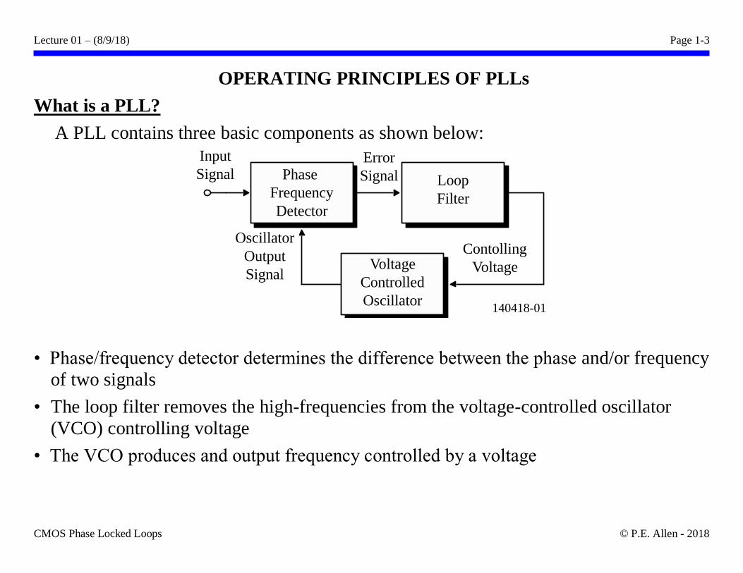
OPERATING PRINCIPLES OF PLLs
What is a PLL?
A PLL contains three basic components as shown below:
• Phase/frequency detector determines the difference between the phase and/or frequency
of two signals
• The loop filter removes the high-frequencies from the voltage-controlled oscillator
(VCO) controlling voltage
• The VCO produces and output frequency controlled by a voltage
Phase
Frequency
Detector
Loop
Filter
Voltage
Controlled
Oscillator
Input
SignalError
Signal
Contolling
Voltage
Oscillator
Output
Signal
140418-01
Lecture 01 – (8/9/18) Page 1-4
CMOS Phase Locked Loops © P.E. Allen - 2018
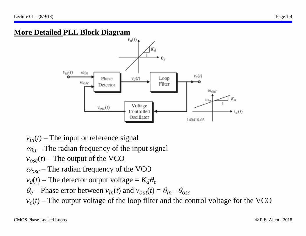
More Detailed PLL Block Diagram
vin(t) – The input or reference signal
in – The radian frequency of the input signal
vosc(t) – The output of the VCO
osc – The radian frequency of the VCO
vd(t) – The detector output voltage = Kde
e – Phase error between vin(t) and vout(t) = in - osc
vc(t) – The output voltage of the loop filter and the control voltage for the VCO
Lecture 01 – (8/9/18) Page 1-5
CMOS Phase Locked Loops © P.E. Allen - 2018
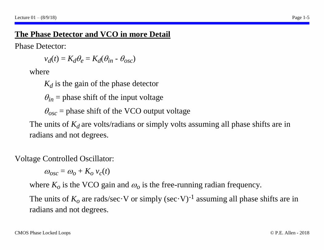
The Phase Detector and VCO in more Detail
Phase Detector:
vd(t) = Kde = Kd(in - osc)
where
Kd is the gain of the phase detector
in = phase shift of the input voltage
osc = phase shift of the VCO output voltage
The units of Kd are volts/radians or simply volts assuming all phase shifts are in
radians and not degrees.
Voltage Controlled Oscillator:
osc = o + Ko vc(t)
where Ko is the VCO gain and o is the free-running radian frequency.
The units of Ko are rads/sec·V or simply (sec·V)-1 assuming all phase shifts are in
radians and not degrees.
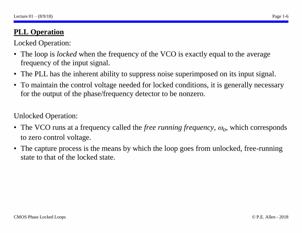
Lecture 01 – (8/9/18) Page 1-6
CMOS Phase Locked Loops © P.E. Allen - 2018
PLL Operation
Locked Operation:
• The loop is locked when the frequency of the VCO is exactly equal to the average
frequency of the input signal.
• The PLL has the inherent ability to suppress noise superimposed on its input signal.
• To maintain the control voltage needed for locked conditions, it is generally necessary
for the output of the phase/frequency detector to be nonzero.
Unlocked Operation:
• The VCO runs at a frequency called the free running frequency, o, which corresponds
to zero control voltage.
• The capture process is the means by which the loop goes from unlocked, free-running
state to that of the locked state.
Lecture 01 – (8/9/18) Page 1-7
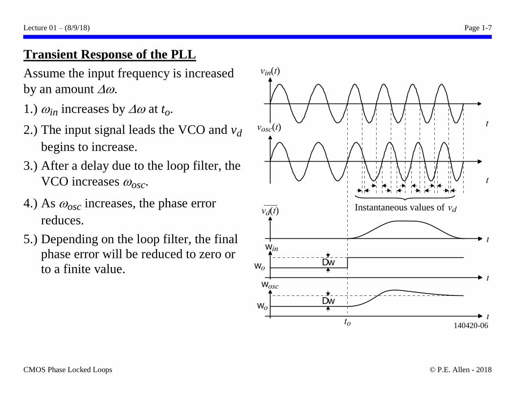
CMOS Phase Locked Loops © P.E. Allen - 2018
Transient Response of the PLL
Assume the input frequency is increased
by an amount .
1.) in increases by at to.
2.) The input signal leads the VCO and vd
begins to increase.
3.) After a delay due to the loop filter, the
VCO increases osc.
4.) As osc increases, the phase error
reduces.
5.) Depending on the loop filter, the final
phase error will be reduced to zero or
to a finite value.
vin(t)
vosc(t)
vd(t)
t
t
t
twosc
win
t
wo
wo
Dw
Dw
to
Instantaneous values of vd
140420-06

Lecture 01 – (8/9/18) Page 1-8
CMOS Phase Locked Loops © P.E. Allen - 2018
CLASSIFICATION OF PLL TYPES
Types of PLLs
PLL Type Phase Detector Loop Filter Controlled Oscillator
Linear PLL (LPLL) Analog multiplier RC passive or active Voltage
Digital PLL (DPLL) Digital detector RC passive or active Voltage
All digital PLL
(ADPLL)
Digital detector Digital filter Digitally controlled
Software PLL
(SPLL)
Software multiplier Software filter Software oscillator
The digital PLL (DPLL) has been the mainstay of most PLLs and is called the “classical”
digital PLL.

Lecture 01 – (8/9/18) Page 1-9
CMOS Phase Locked Loops © P.E. Allen - 2018
The Linear PLL (LPLL)
• Uses a analog multiplier for the PDF
• Loop filter is active or passive analog
• VCO is analog
Analog
Multiplier
Analog
Loop
Filter
Voltage
Controlled
Oscillator
Input
SignalError
Signal
Controlling
Voltage
Oscillator
Output
Signal
140418-04

Lecture 01 – (8/9/18) Page 1-10
CMOS Phase Locked Loops © P.E. Allen - 2018
The Digital PLL (DPLL)
• Phase detector is digital
• Loop filter is passive of active analog
• VCO is analog
• Called the “Classical Digital PLL”
Digital
Detector
Analog
Loop
Filter
Voltage
Controlled
Oscillator
Input
Signal Error
SignalControlling
Voltage
Oscillator
Output
Signal
140418-05
¸N
Counter
(optional)
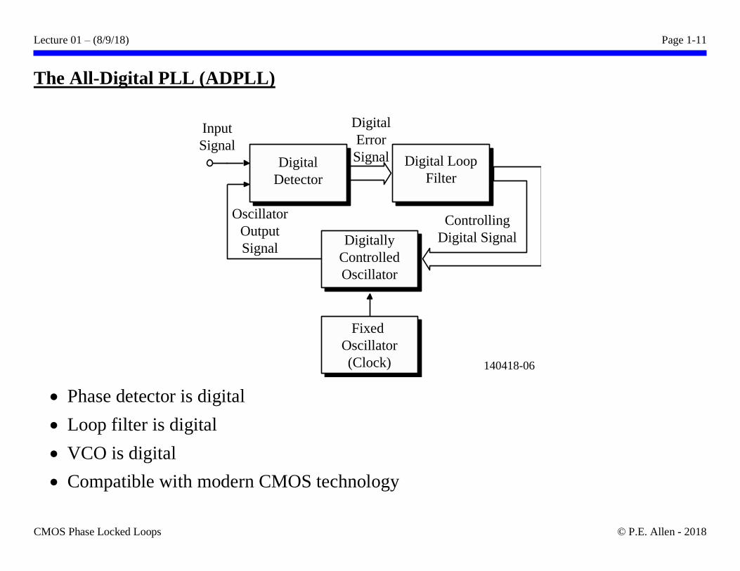
Lecture 01 – (8/9/18) Page 1-11
CMOS Phase Locked Loops © P.E. Allen - 2018
The All-Digital PLL (ADPLL)
• Phase detector is digital
• Loop filter is digital
• VCO is digital
• Compatible with modern CMOS technology
Digital
Detector
Digital Loop
Filter
Digitally
Controlled
Oscillator
Input
Signal
Digital
Error
Signal
Controlling
Digital Signal
Oscillator
Output
Signal
140418-06
Fixed
Oscillator
(Clock)

Lecture 01 – (8/9/18) Page 1-12
CMOS Phase Locked Loops © P.E. Allen - 2018
The Software PLL (SPLL)
• Phase detector is implemented in software
• Loop filter is implemented in software
• Oscillator is implemented in software driven by an external clock
• Requires analog to digital conversion at the input and digital to analog conversion at
the output
• Software permits reconfiguring of the PLL
Software
PLL
Analog-
Digital
Converter
Input
Signal
Clock
Digital-
Analog
Converter
Output
Signal
140418-07
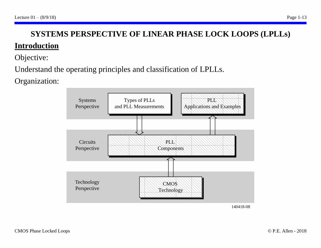
Lecture 01 – (8/9/18) Page 1-13
CMOS Phase Locked Loops © P.E. Allen - 2018
SYSTEMS PERSPECTIVE OF LINEAR PHASE LOCK LOOPS (LPLLs)
Introduction
Objective:
Understand the operating principles and classification of LPLLs.
Organization:
PLL
Applications and Examples
Systems
Perspective
Circuits
Perspective
140418-08
PLL
Components
Types of PLLs
and PLL Measurements
Technology
PerspectiveCMOS
Technology

Lecture 01 – (8/9/18) Page 1-14
CMOS Phase Locked Loops © P.E. Allen - 2018
Outline
• LPLL Blocks
• Locked State
• Order of the LPLL System
• The Acquisition Process - Unlocked State
• Noise in the LPLL
• LPLL System Design
• Simulation of LPLLs
Lecture 01 – (8/9/18) Page 1-15
CMOS Phase Locked Loops © P.E. Allen - 2018
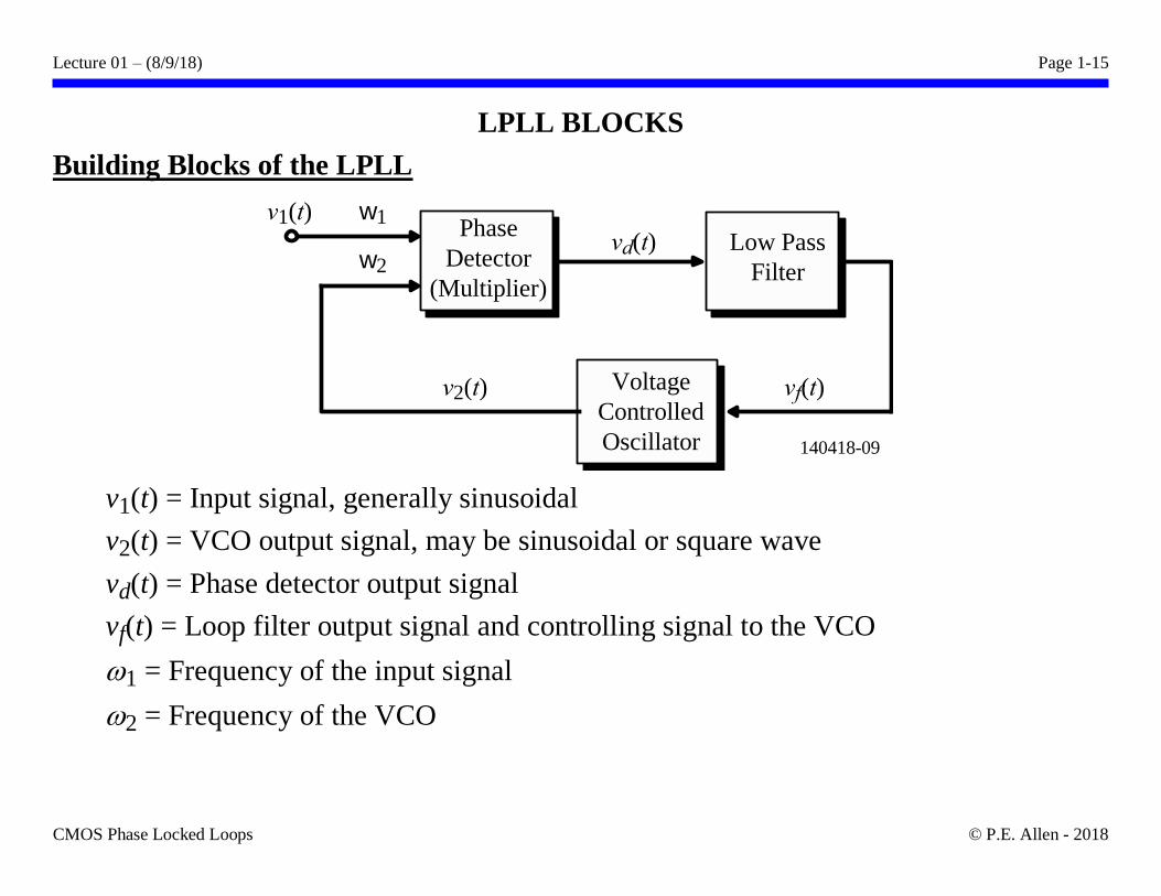
LPLL BLOCKS
Building Blocks of the LPLL
v1(t) = Input signal, generally sinusoidal
v2(t) = VCO output signal, may be sinusoidal or square wave
vd(t) = Phase detector output signal
vf(t) = Loop filter output signal and controlling signal to the VCO
1 = Frequency of the input signal
2 = Frequency of the VCO
Low Pass
Filter
Voltage
Controlled
Oscillator
v1(t) w1
w2vd(t)
140418-09
Phase
Detector
(Multiplier)
v2(t) vf(t)
Lecture 01 – (8/9/18) Page 1-16
CMOS Phase Locked Loops © P.E. Allen - 2018
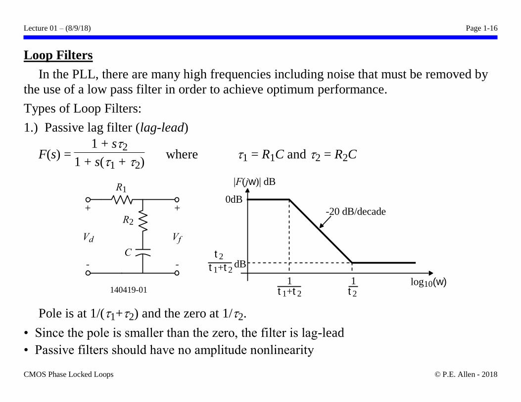
Loop Filters
In the PLL, there are many high frequencies including noise that must be removed by
the use of a low pass filter in order to achieve optimum performance.
Types of Loop Filters:
1.) Passive lag filter (lag-lead)
F(s) = 1 + s2
1 + s(1 + 2) where 1 = R1C and 2 = R2C
Pole is at 1/(1+2) and the zero at 1/2.
• Since the pole is smaller than the zero, the filter is lag-lead
• Passive filters should have no amplitude nonlinearity
Vf
R1
R2
C
+
-
Vd
+
-
|F(jw)| dB
0dB
1t1+t2
1t2
t1+t2
t2dB
log10(w)140419-01
-20 dB/decade
Lecture 01 – (8/9/18) Page 1-17
CMOS Phase Locked Loops © P.E. Allen - 2018
Loop Filters - Continued
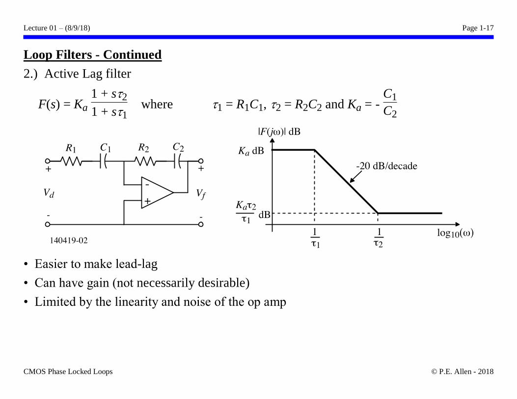
2.) Active Lag filter
F(s) = Ka 1 + s2
1 + s1 where 1 = R1C1, 2 = R2C2 and Ka = -
C1
C2
• Easier to make lead-lag
• Can have gain (not necessarily desirable)
• Limited by the linearity and noise of the op amp
Lecture 01 – (8/9/18) Page 1-18
CMOS Phase Locked Loops © P.E. Allen - 2018
Loop Filters - Continued
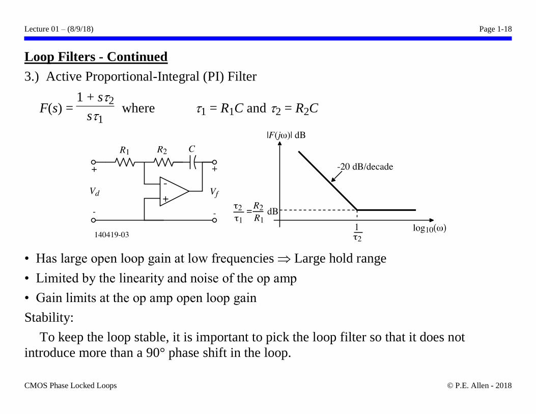
3.) Active Proportional-Integral (PI) Filter
F(s) = 1 + s2
s1 where 1 = R1C and 2 = R2C
• Has large open loop gain at low frequencies Large hold range
• Limited by the linearity and noise of the op amp
• Gain limits at the op amp open loop gain
Stability:
To keep the loop stable, it is important to pick the loop filter so that it does not
introduce more than a 90° phase shift in the loop.

Lecture 01 – (8/9/18) Page 1-19
CMOS Phase Locked Loops © P.E. Allen - 2018
Phase Signals
It is important to remember that frequency and phase are related as
ddt
= → = ·dt
Transfer functions:
H(s) = V2(s)
V1(s)
where V2(s) and V1(s) are the Laplace transforms of v2(t) and v1(t).
To examine phase signals, let us assume that,
v1(t) = V10 sin[1t + 1(t)] and v2(t) = V20 sin[2t + 2(t)]
For phase signals, the information is carried only in (t).
Next, we consider some simple phase signals that are used to excite a PLL.

Lecture 01 – (8/9/18) Page 1-20
CMOS Phase Locked Loops © P.E. Allen - 2018
Phase Signals – Continued
1.) A step phase shift which is an example of phase
modulation.
1(t) = u(t)
2.) A step frequency change assuming that 1(t) = o
for t < 0. We may express v1(t) as,
v1(t) = V10 sin[ot + ·t]
= V10 sin[ot + 1(t)]
1(t) = ·t
(the phase becomes a ramp signal)
v1(t)
t
q1(t)
tDF
140419-04
v1(t)
t
w1(t)
tDw
140419-05
q1(t)
tDw
Lecture 01 – (8/9/18) Page 1-21
CMOS Phase Locked Loops © P.E. Allen - 2018
Phase Signals – Continued
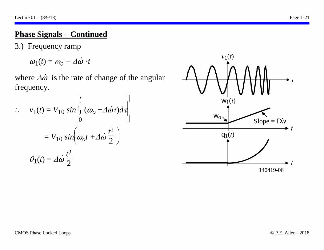
3.) Frequency ramp
1(t) = o + · ·t
where · is the rate of change of the angular
frequency.
v1(t) = V10 sin
0
t
(o + ·)d
= V10 sin
ot + · t2
2
1(t) = · t2
2
v1(t)
t
w1(t)
t
wo
140419-06
q1(t)
t
Slope = Dw.
Lecture 01 – (8/9/18) Page 1-22
CMOS Phase Locked Loops © P.E. Allen - 2018
SUMMARY
• LPLL blocks are:
1.) Multiplying phase detector
2.) Low pass filter
3.) Voltage controlled oscillator
• Locked state: Input frequency = VCO frequency
The phase response is low pass
The phase error response is high pass


![(Reference [2]) LINEAR PHASE LOCKED LOOPS - CONTINUED …pallen.ece.gatech.edu/Academic/ECE_6440/Summer_2003/L060-LPLL-II(2UP).pdf(Reference [2]) LINEAR PHASE LOCKED LOOPS - CONTINUED](https://img.pdfslide.net/doc/110x75/6016ce84e4e4bb557426a4e4/reference-2-linear-phase-locked-loops-continued-2uppdf-reference-2-linear.jpg)


![RF Module Design - [Chapter 8] Phase-Locked Loops](https://img.pdfslide.net/doc/110x75/55cebb77bb61eba32f8b45bd/rf-module-design-chapter-8-phase-locked-loops.jpg)


