Embed Size (px)
Citation preview
Lecture 18 –Optical Lithography 3 - Resist
EECS 598-002 Winter 2006Nanophotonics and Nano-scale Fabrication
P.C.Ku
2EECS 598-002 Nanophotonics and Nanoscale Fabrication by P.C.Ku
Photoresist
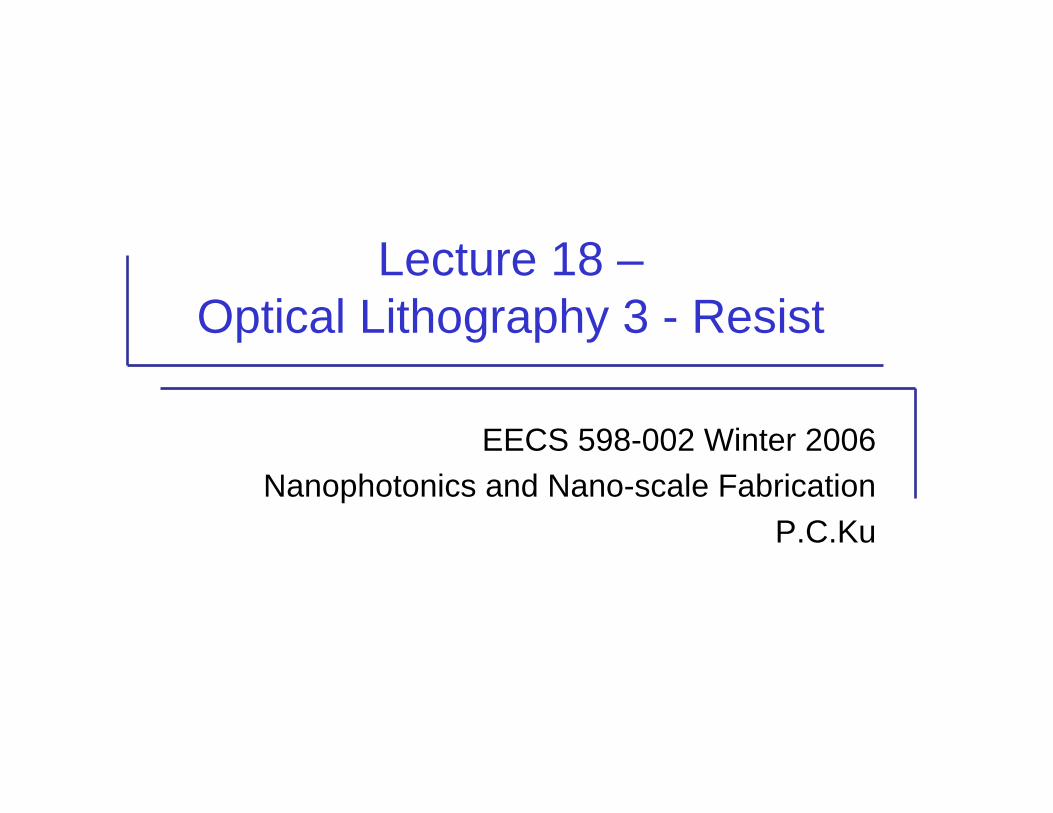
The most commonly used photoresist nowadays is a two-component system which consists of the novolac resin and the diazonaphthoquinone photoactive compound (PAC; a dissolution inhibitor).
novalac PAC
1. Inert to photochemistry2. For film-forming3. For adhesion4. For chemical resistance5. For thermal resistance
1. Responsible for photochemistry2. Quantum efficiency:
# of molecules transformed# of photons absorbed
φ =
Not the total intensity!
3EECS 598-002 Nanophotonics and Nanoscale Fabrication by P.C.Ku
Chemically amplified DUV resist
Since the quantum efficiency of a regular resist is ~ 100 fold smaller at the DUV wavelength, chemical amplification is used.Instead of optically destroying the dissolution inhibitors, chemically amplified DUV resist creates acid by photochemical reactions. Acid then destroys the inhibitor at an elevated temperature (PEB). Each acid molecule can trigger the catalysis event to destroy several inhibitors
amplification.
Ref: H. Ito, “Chemical amplification resists,” IBM J. R&D, 41 (1997)

4EECS 598-002 Nanophotonics and Nanoscale Fabrication by P.C.Ku
Resist process overviewAdhesion promotionor BARC coating
Resist coating
Softbake (SB)
Exposure
Post-exposure bake (PEB)
Resist development
Rinse and dry
Metrology (CD & REG)
bad good
EtchResist/BARC removal
TEBR
OEBR
5EECS 598-002 Nanophotonics and Nanoscale Fabrication by P.C.Ku
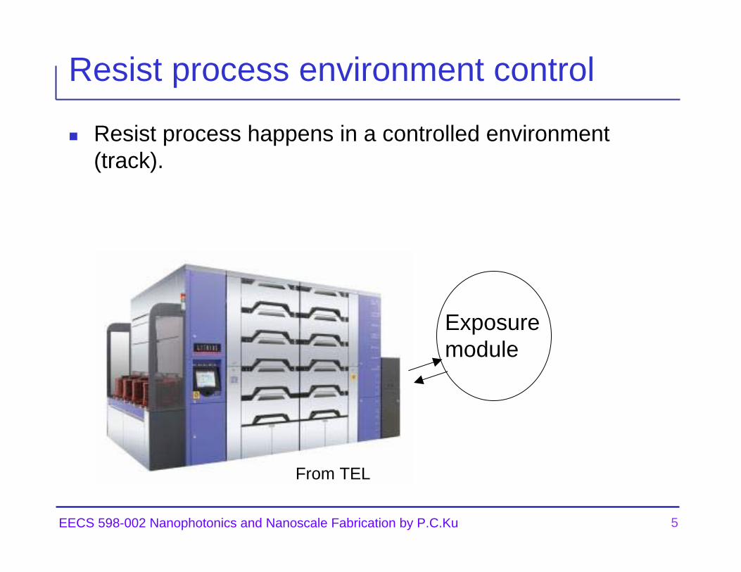
Resist process environment control
Resist process happens in a controlled environment (track).
From TEL
Exposuremodule
6EECS 598-002 Nanophotonics and Nanoscale Fabrication by P.C.Ku
Adhesion promotion
The most common adhesion promoter is HMDS (hexamethylenedisiloxane). Applied in vapor phase (100-160。C.
7EECS 598-002 Nanophotonics and Nanoscale Fabrication by P.C.Ku
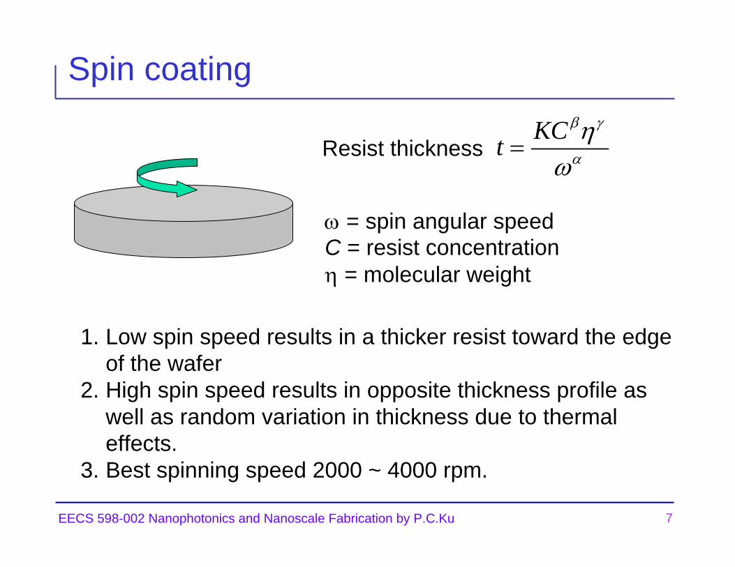
Spin coating
KCtβ γ
α
ηω
=Resist thickness
ω = spin angular speedC = resist concentrationη = molecular weight
1. Low spin speed results in a thicker resist toward the edgeof the wafer
2. High spin speed results in opposite thickness profile as well as random variation in thickness due to thermal effects.
3. Best spinning speed 2000 ~ 4000 rpm.
8EECS 598-002 Nanophotonics and Nanoscale Fabrication by P.C.Ku
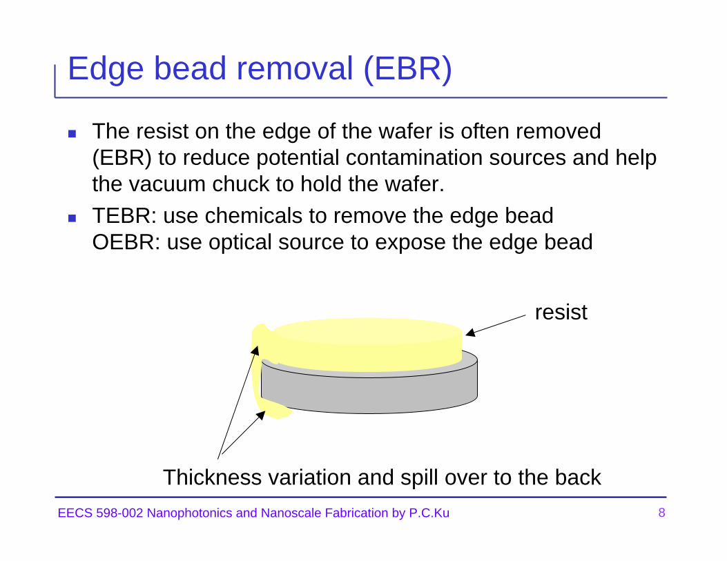
Edge bead removal (EBR)
The resist on the edge of the wafer is often removed (EBR) to reduce potential contamination sources and help the vacuum chuck to hold the wafer.TEBR: use chemicals to remove the edge beadOEBR: use optical source to expose the edge bead
resist
Thickness variation and spill over to the back
9EECS 598-002 Nanophotonics and Nanoscale Fabrication by P.C.Ku
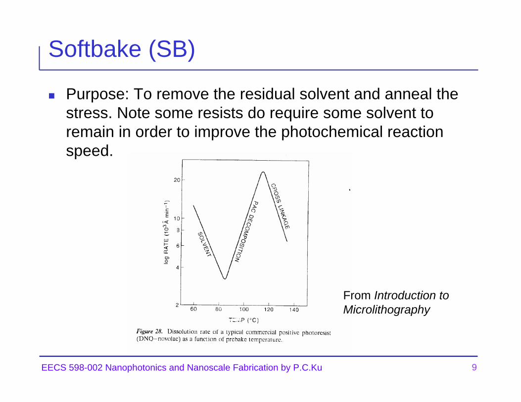
Softbake (SB)
Purpose: To remove the residual solvent and anneal the stress. Note some resists do require some solvent to remain in order to improve the photochemical reaction speed.
From Introduction toMicrolithography
10EECS 598-002 Nanophotonics and Nanoscale Fabrication by P.C.Ku
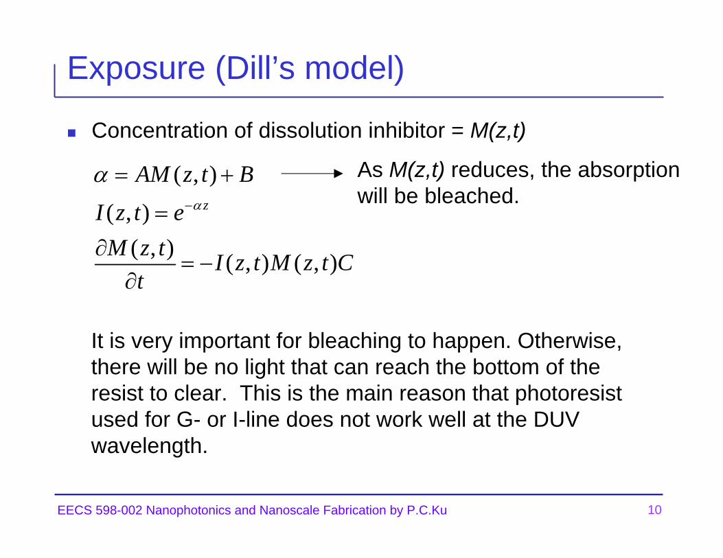
Exposure (Dill’s model)
Concentration of dissolution inhibitor = M(z,t)
( , )( , )
( , ) ( , ) ( , )
z
AM z t BI z t eM z t I z t M z t C
t
α
α−
= +
=∂
= −∂
As M(z,t) reduces, the absorptionwill be bleached.
It is very important for bleaching to happen. Otherwise,there will be no light that can reach the bottom of the resist to clear. This is the main reason that photoresistused for G- or I-line does not work well at the DUVwavelength.
11EECS 598-002 Nanophotonics and Nanoscale Fabrication by P.C.Ku
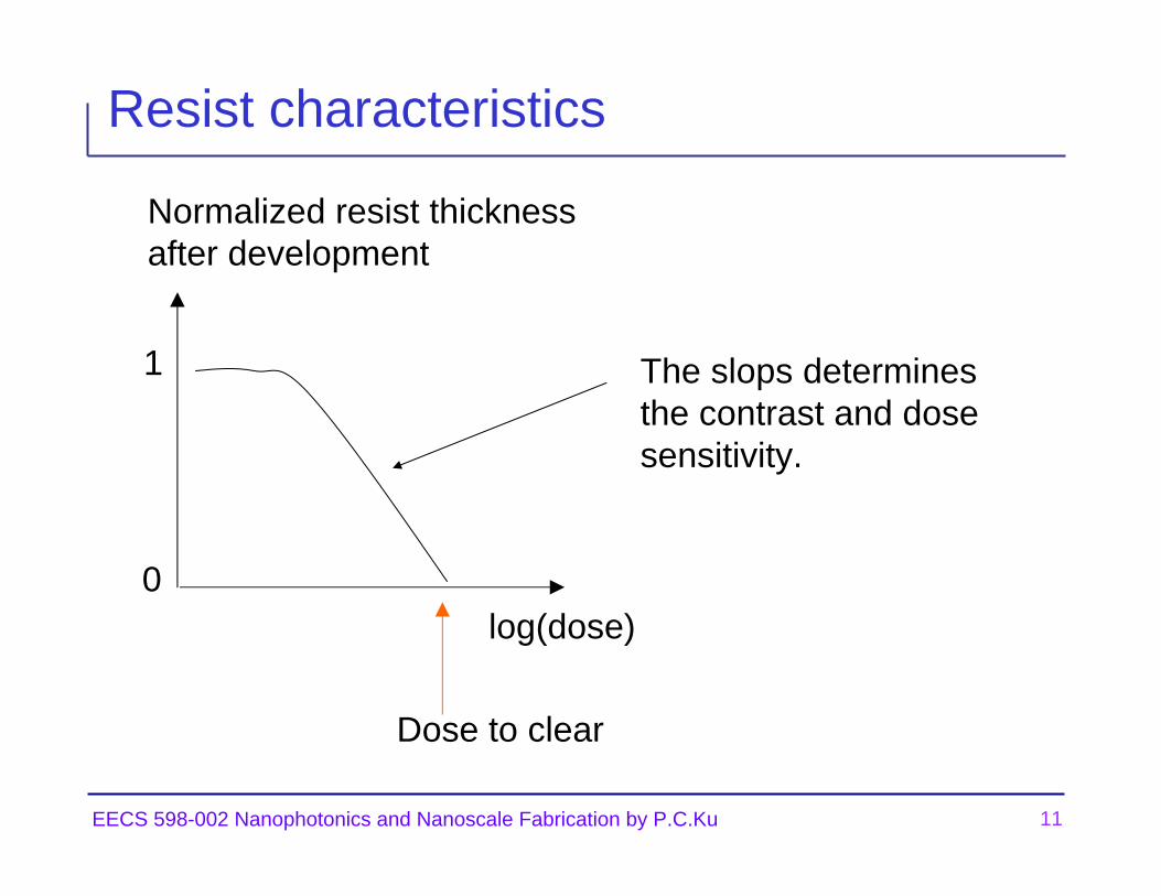
Resist characteristics
log(dose)
Normalized resist thicknessafter development
1
0
Dose to clear
The slops determinesthe contrast and dosesensitivity.
12EECS 598-002 Nanophotonics and Nanoscale Fabrication by P.C.Ku
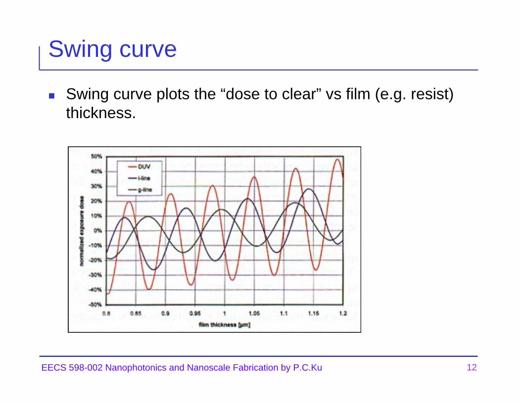
Swing curve
Swing curve plots the “dose to clear” vs film (e.g. resist) thickness.
13EECS 598-002 Nanophotonics and Nanoscale Fabrication by P.C.Ku
Post exposure bake (PEB)
PEB is different from the “hardbake” before an etching process.PEB is used to induce the diffusion of photogeneratedcompound in order to smooth out the interference effect on the resist profile.
14EECS 598-002 Nanophotonics and Nanoscale Fabrication by P.C.Ku
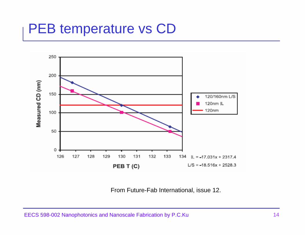
PEB temperature vs CD
From Future-Fab International, issue 12.
15EECS 598-002 Nanophotonics and Nanoscale Fabrication by P.C.Ku
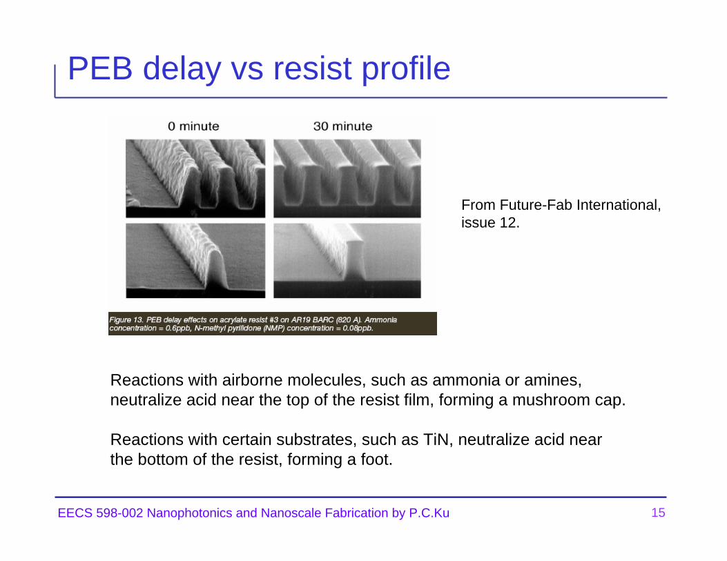
PEB delay vs resist profile
Reactions with airborne molecules, such as ammonia or amines,neutralize acid near the top of the resist film, forming a mushroom cap.
Reactions with certain substrates, such as TiN, neutralize acid nearthe bottom of the resist, forming a foot.
From Future-Fab International,issue 12.
16EECS 598-002 Nanophotonics and Nanoscale Fabrication by P.C.Ku
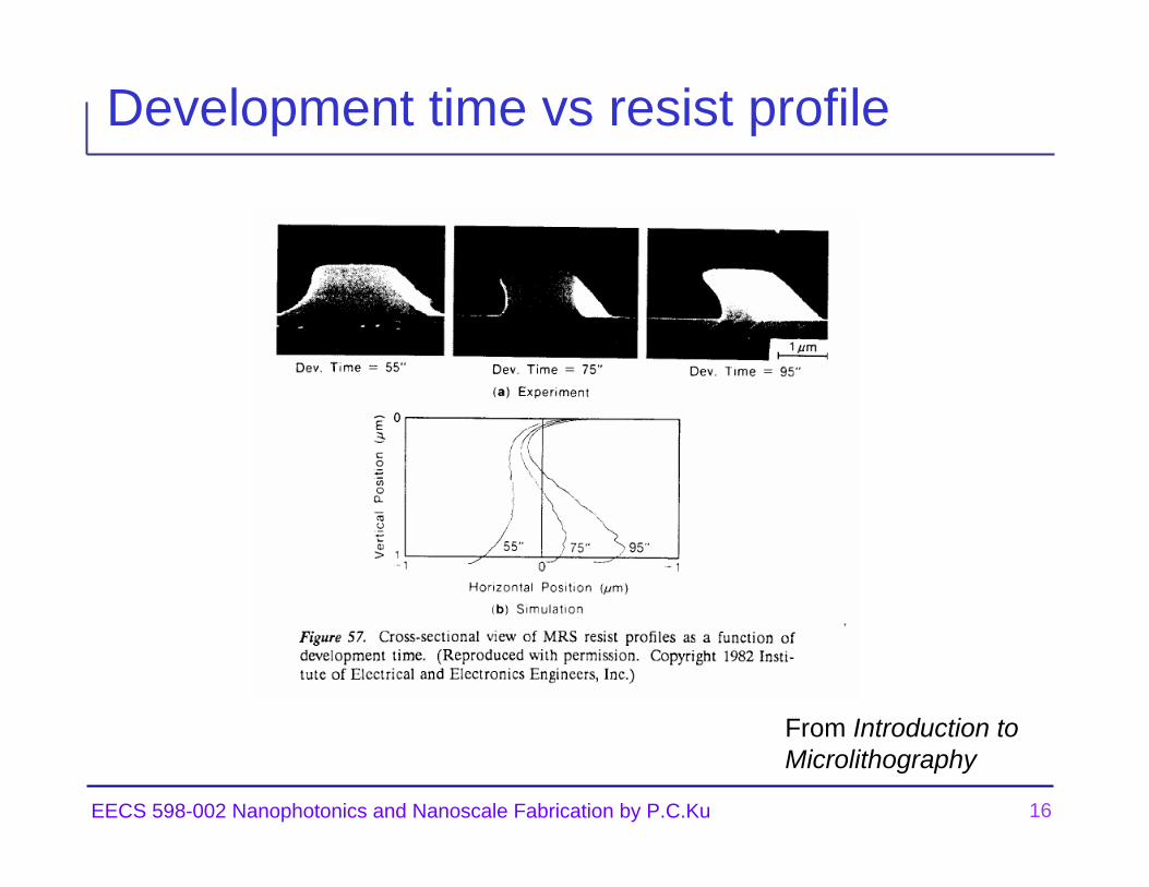
Development time vs resist profile
From Introduction toMicrolithography
17EECS 598-002 Nanophotonics and Nanoscale Fabrication by P.C.Ku
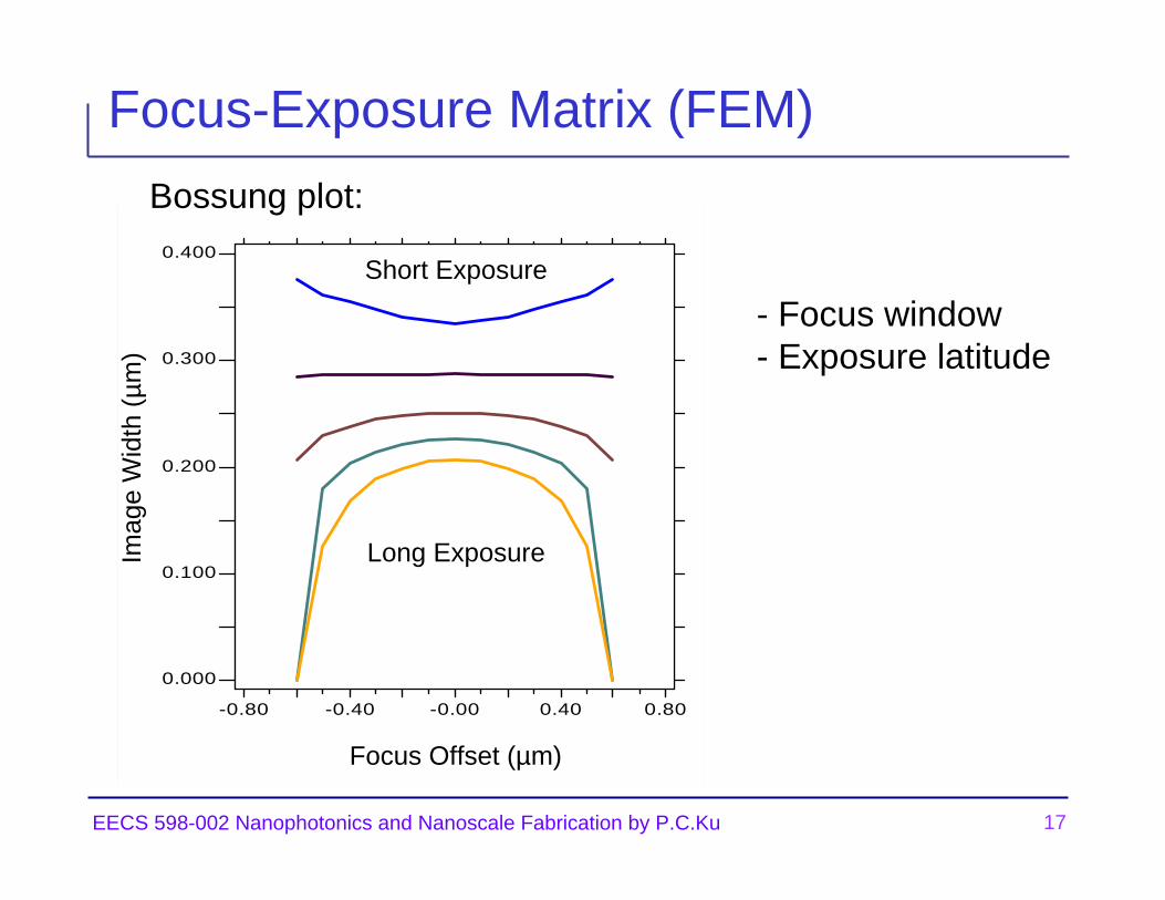
-0.80 -0.40 -0.00 0.40 0.80
0.000
0.100
0.200
0.300
0.400
Focus Offset (µm)
Imag
e W
idth
(µm
)
Long Exposure
Short Exposure
Focus-Exposure Matrix (FEM)
- Focus window- Exposure latitude
Bossung plot:
18EECS 598-002 Nanophotonics and Nanoscale Fabrication by P.C.Ku
Metrology
Registration: overlay measurementCD
19EECS 598-002 Nanophotonics and Nanoscale Fabrication by P.C.Ku
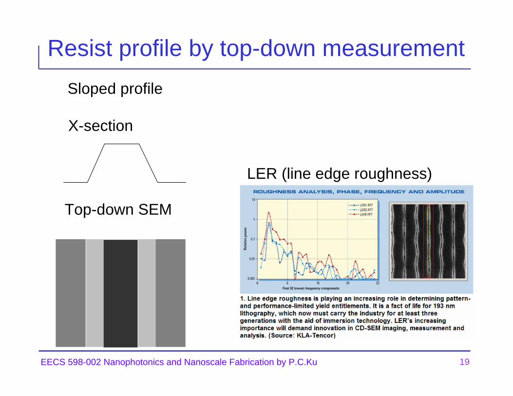
Resist profile by top-down measurement
LER (line edge roughness)
Sloped profile
X-section
Top-down SEM

![Evidence for photogenerated intermediate hole polarons in ZnOth.fhi-berlin.mpg.de/site/uploads/Publications/51428_2_merged_1426091264.pdfdoping) [16]. Since spectra recorded after](https://img.pdfslide.net/doc/110x75/5f2338fd8255547b303deaeb/evidence-for-photogenerated-intermediate-hole-polarons-in-znothfhi-doping-16.jpg)