Embed Size (px)
Citation preview

Lecture 2 – Analog circuits
Seeing the light…..
I
t
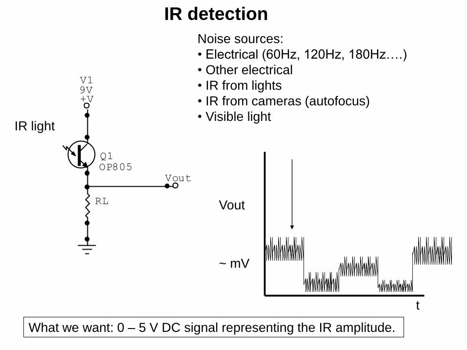
IR detection
IR light
Vout
t
Noise sources:
• Electrical (60Hz, 120Hz, 180Hz….)
• Other electrical
• IR from lights
• IR from cameras (autofocus)
• Visible light
~ mV
Q1
OP805Vout
+V
V19V
RL
What we want: 0 – 5 V DC signal representing the IR amplitude.

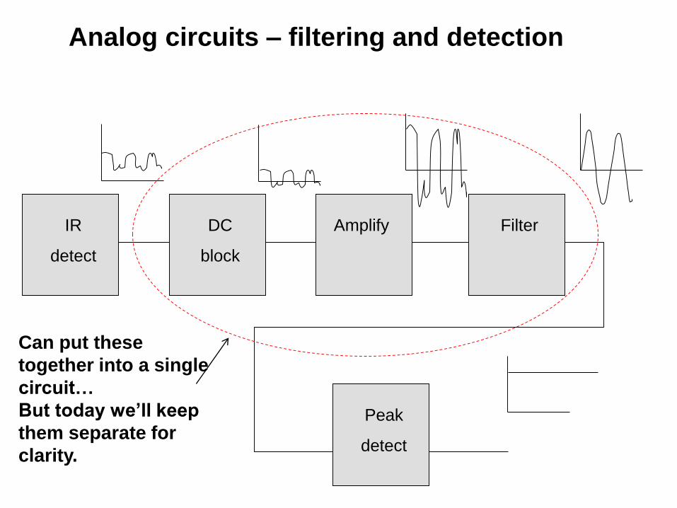
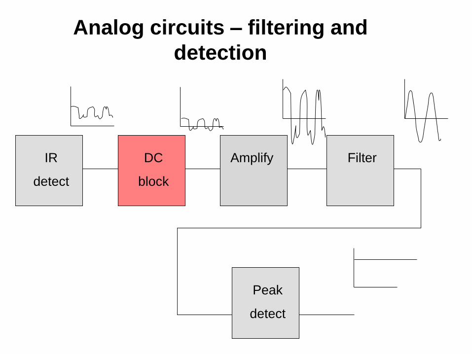
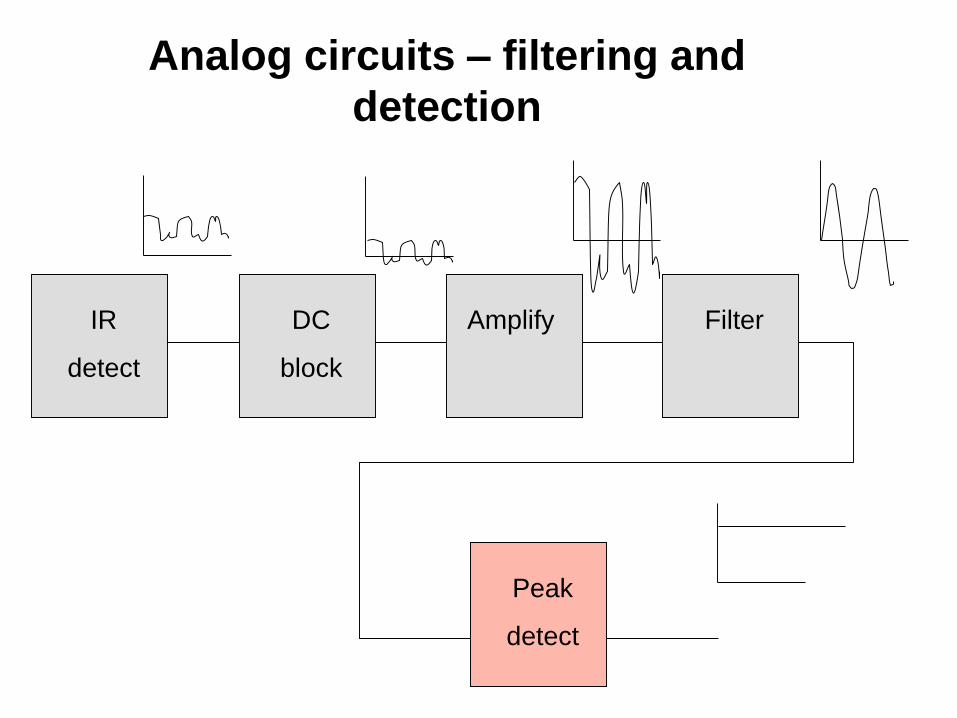
Analog circuits – filtering and detection
IR
detect
DC
block
Amplify Filter
Peak
detect
Analog circuits – filtering and detection
IR
detect
DC
block
Amplify Filter
Peak
detect
Can put these
together into a single
circuit…
But today we’ll keep
them separate for
clarity.

DEMO TIME
IR
detect
DC
block
Amplify Filter
Peak
detect
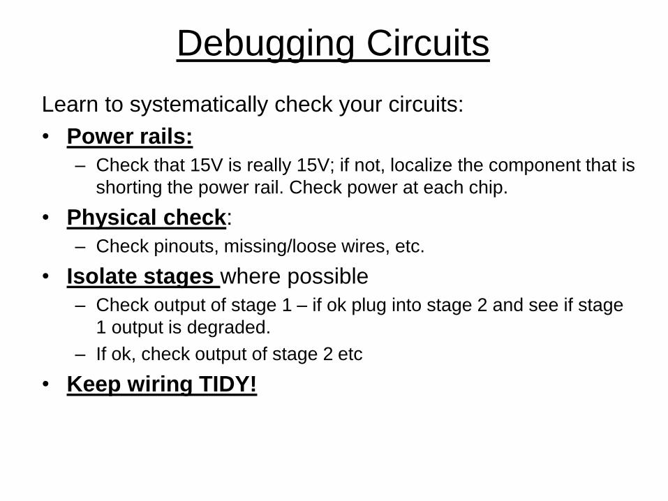
Debugging Circuits
Learn to systematically check your circuits:
• Power rails:
– Check that 15V is really 15V; if not, localize the component that is
shorting the power rail. Check power at each chip.
• Physical check:
– Check pinouts, missing/loose wires, etc.
• Isolate stages where possible
– Check output of stage 1 – if ok plug into stage 2 and see if stage
1 output is degraded.
– If ok, check output of stage 2 etc
• Keep wiring TIDY!
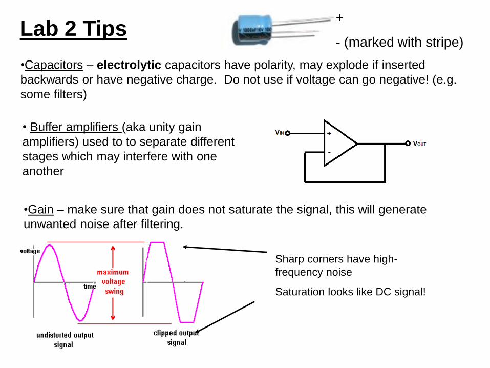
•Capacitors – electrolytic capacitors have polarity, may explode if inserted
backwards or have negative charge. Do not use if voltage can go negative! (e.g.
some filters)
Lab 2 Tips
Sharp corners have high-
frequency noise
Saturation looks like DC signal!
+
- (marked with stripe)
•Gain – make sure that gain does not saturate the signal, this will generate
unwanted noise after filtering.
• Buffer amplifiers (aka unity gain
amplifiers) used to to separate different
stages which may interfere with one
another
Analog circuits – filtering and
detection
IR
detect
DC
block
Amplify Filter
Peak
detect

Q1
OP805Vout
+V
V19V
RL
Analog circuits – discrete devices: BJT
Application: light detection
Phototransistor:
Acts like BJT except charge carriers
generated by incident light add to the
base current.
In other words, Ic Incident light
Ic

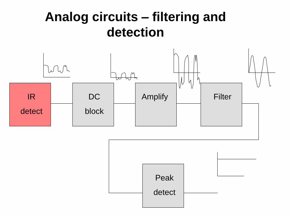
IR detection
Build a circuit that:
• Uses an OP805 and a resistor to detect
variations in light with a voltmeter.
• Determine whether increasing or decreasing the
load resistance makes it more sensitive
Note: OP805 will see some room light – use
your hand to block it, and use the voltmeter to
detect the change in signal.
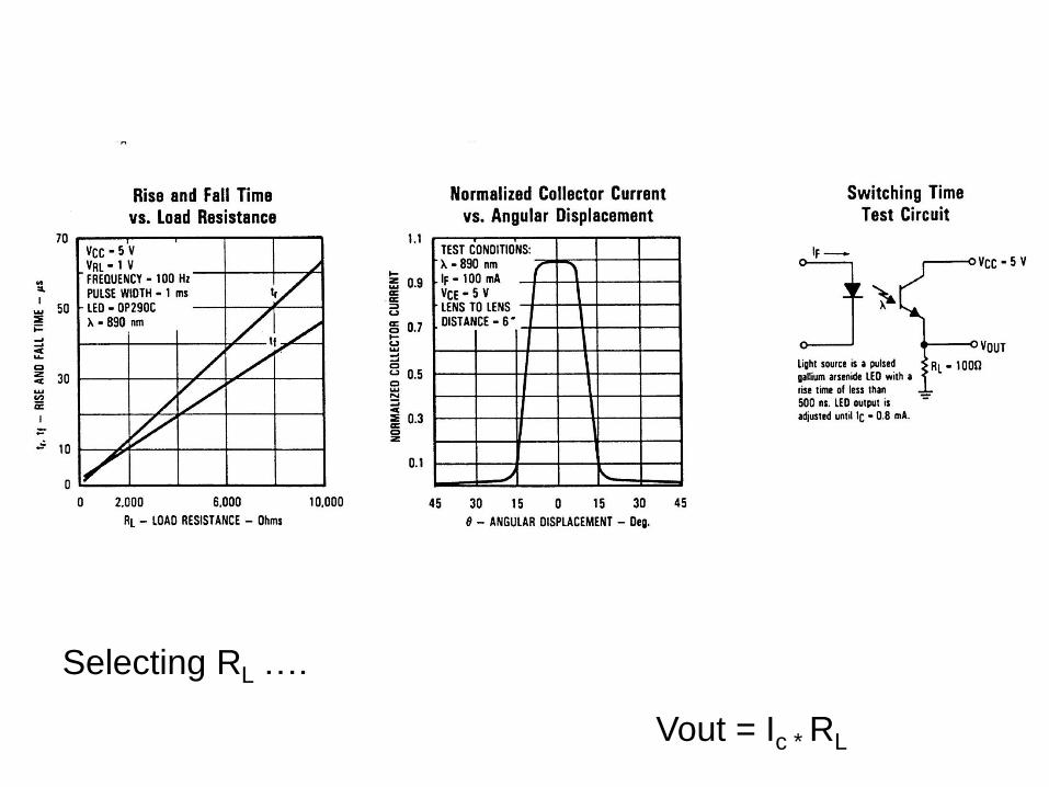
Vout = Ic * RL
+
Selecting RL ….
Analog circuits – filtering and
detection
IR
detect
DC
block
Amplify Filter
Peak
detect
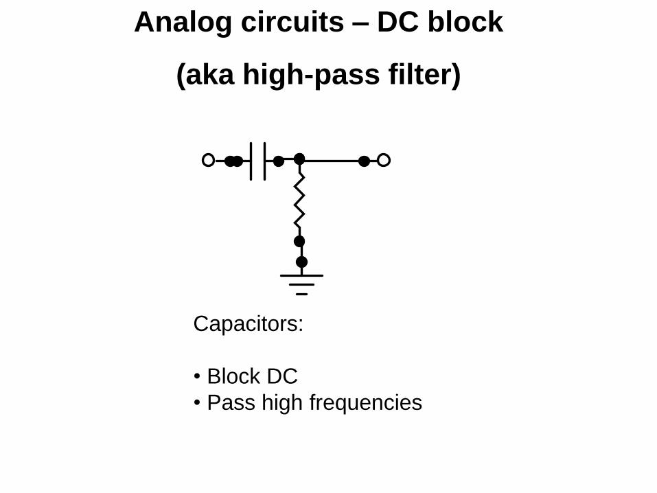
Analog circuits – DC block
(aka high-pass filter)
Capacitors:
• Block DC
• Pass high frequencies
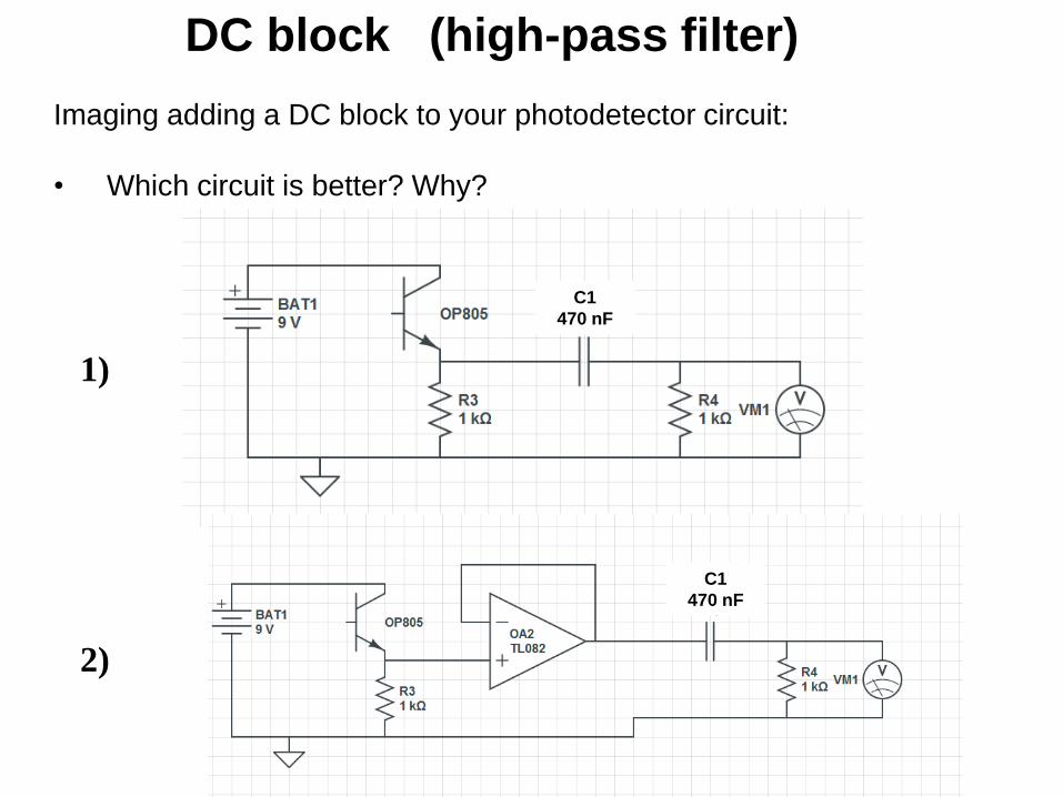
DC block (high-pass filter)
Imaging adding a DC block to your photodetector circuit:
• Which circuit is better? Why?
1)
2)
C1
470 nF
C1
470 nF
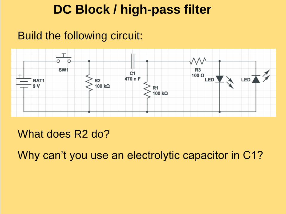
DC Block / high-pass filter
Build the following circuit:
What does R2 do?
Why can’t you use an electrolytic capacitor in C1?

Analog circuits – filtering and
detection
IR
detect
DC
block
Amplify Filter
Peak
detect

Analog circuits – filtering and
detection
What is the result of the following:
+
-Z1
Z2
Z2/Z1=
3
Vout
Vout = 1)
2)
3)
4)

Analog circuits: Op-ampsEg: Inverting
amplifier.+
-V-
VoutV- = 0
I1 = Vin/Z1
Vout = 0 – Z2I1
Vout= - (Z2/Z1) Vin
Z1
Z2
Vin
I1
Eg 1: Z2 = 100kW
Z1 = 10kW Vout= - 10 Vin
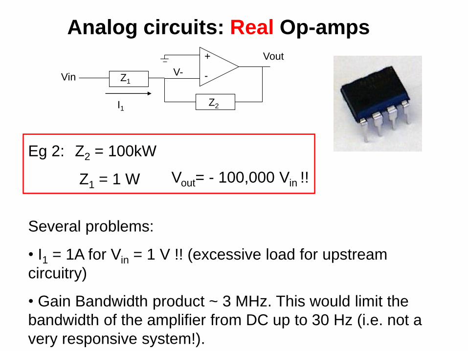
Eg 2: Z2 = 100kW
Z1 = 1 W Vout= - 100,000 Vin !!
Not likely….
10x gain is a
“reasonable” value
Analog circuits: Real Op-amps
+
-V-
Vout
Z1
Z2
Vin
I1
Eg 2: Z2 = 100kW
Z1 = 1 W Vout= - 100,000 Vin !!
Several problems:
• I1 = 1A for Vin = 1 V !! (excessive load for upstream
circuitry)
• Gain Bandwidth product ~ 3 MHz. This would limit the
bandwidth of the amplifier from DC up to 30 Hz (i.e. not a
very responsive system!).
Analog circuits: Real Op-amps
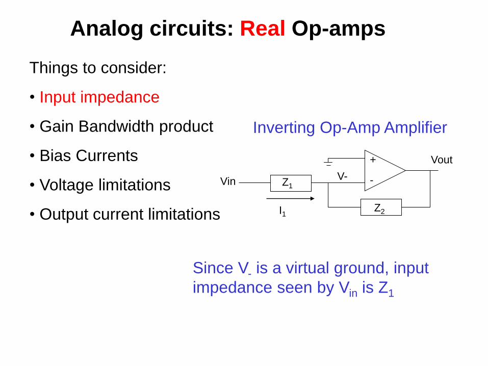
Things to consider:
• Input impedance
• Gain Bandwidth product
• Bias Currents
• Voltage limitations
• Output current limitations
+
-V-
Vout
Z1
Z2
Vin
I1
Since V- is a virtual ground, input
impedance seen by Vin is Z1
Inverting Op-Amp Amplifier

Things to consider:
• Input impedance
• Gain Bandwidth product
• Bias Currents
• Voltage limitations
• Output current limitations
Analog circuits: Real Op-amps
+
-V-
VoutVin
Since Op-amp inputs source or sink very little current
(depends on type) , input impedance in this case is very
high. This is a commonly used buffer to separate your low
impedance circuit from a sensitive source that you need
to measure without drawing current.
Buffer Amplifier aka unity
gain amplifier

Things to consider:
• Input impedance
• Gain Bandwidth product
• Bias Currents
• Voltage limitations
• Output current limitations
Analog circuits: Real Op-amps
+
-V-
Vout
Z1
Z2
Vin
I1
Open loop gain (K)
Frequency 20
100
kHz
Gain-Bandwidth limit (Hz) = Gain * Max. Frequency = CONSTANT
Slew-rate is a similar
limit: it is a limit on the
rate of change of output
voltage
log K
log w
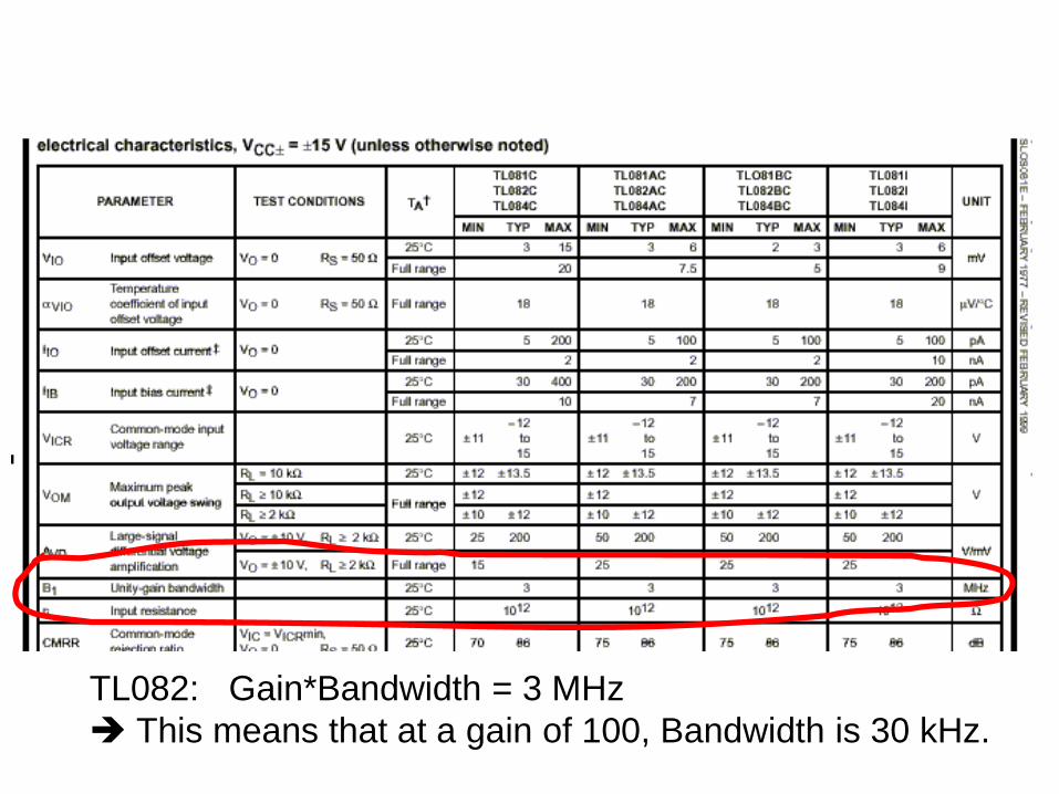
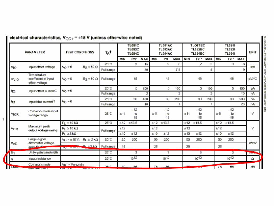
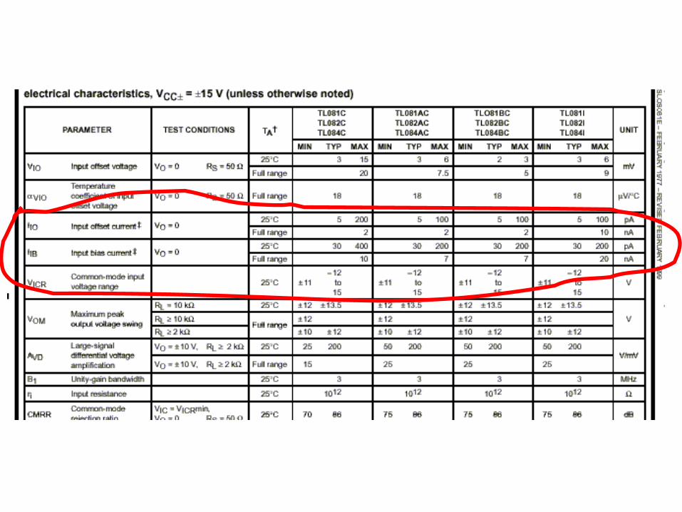
TL082: Gain*Bandwidth = 3 MHz
This means that at a gain of 100, Bandwidth is 30 kHz.
Analog circuits: Real Op-amps
Things to consider:
• Input impedance
• Gain Bandwidth product
• Bias Currents
• Voltage limitations
• Output current limitations
+
-V-
Vout
Z1
Z2
Vin
I1
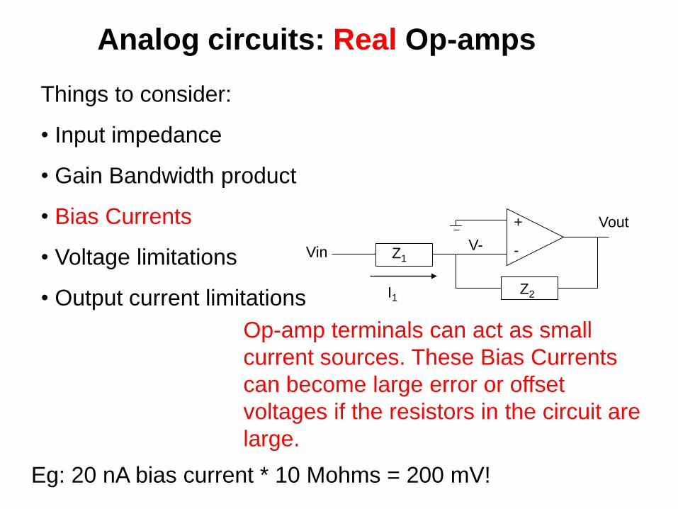
Op-amp terminals can act as small
current sources. These Bias Currents
can become large error or offset
voltages if the resistors in the circuit are
large.
Eg: 20 nA bias current * 10 Mohms = 200 mV!
Analog circuits: Real Op-amps
Things to consider:
• Input impedance
• Gain Bandwidth product
• Bias Currents
• Voltage limitations
• Output current limitations
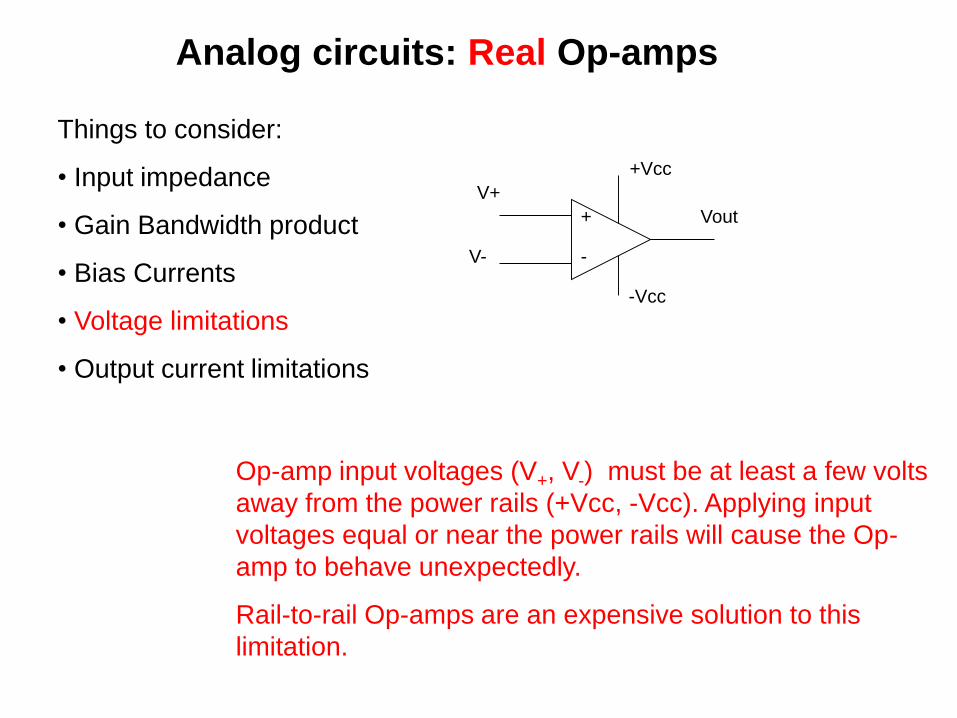
Op-amp input voltages (V+, V-) must be at least a few volts
away from the power rails (+Vcc, -Vcc). Applying input
voltages equal or near the power rails will cause the Op-
amp to behave unexpectedly.
Rail-to-rail Op-amps are an expensive solution to this
limitation.
+
-
-Vcc
Vout
V+
V-
+Vcc
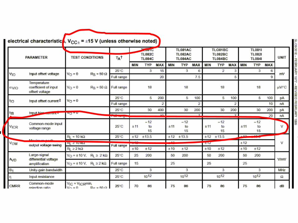
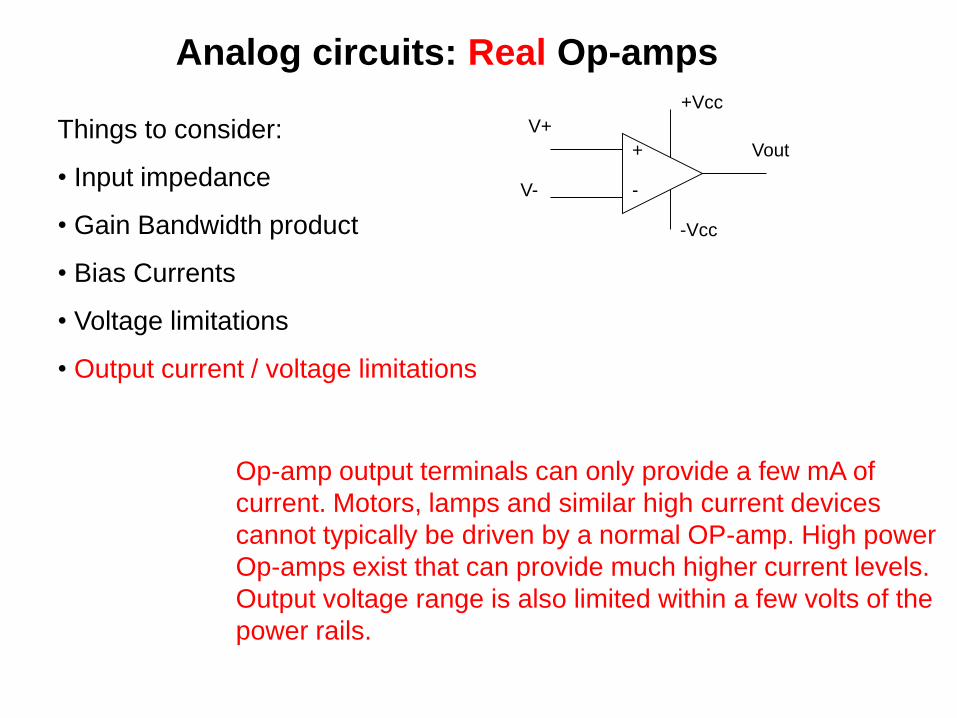
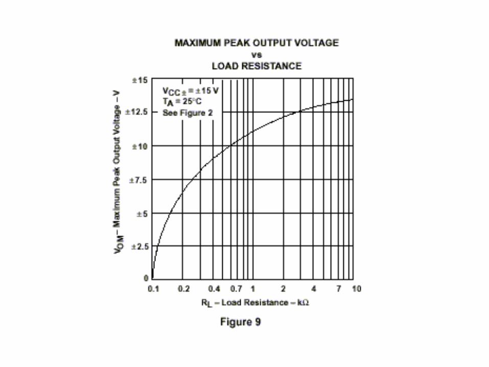
Analog circuits: Real Op-amps
Things to consider:
• Input impedance
• Gain Bandwidth product
• Bias Currents
• Voltage limitations
• Output current / voltage limitations
Op-amp output terminals can only provide a few mA of
current. Motors, lamps and similar high current devices
cannot typically be driven by a normal OP-amp. High power
Op-amps exist that can provide much higher current levels.
Output voltage range is also limited within a few volts of the
power rails.
+
-
-Vcc
Vout
V+
V-
+Vcc
Analog circuits: Real Op-amps
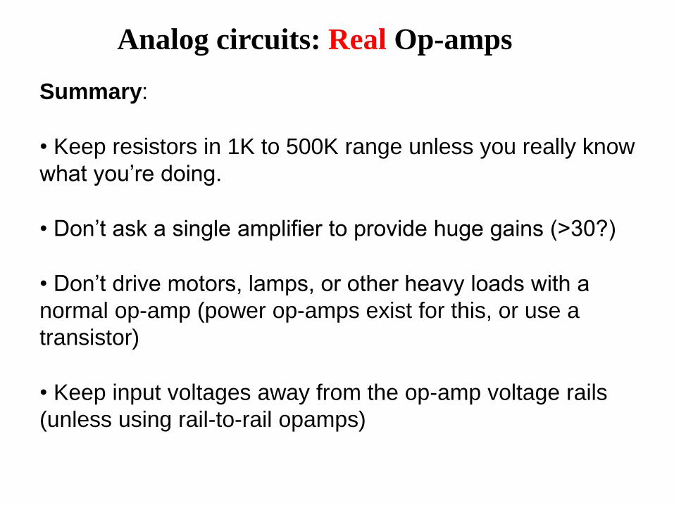
Summary:
• Keep resistors in 1K to 500K range unless you really know
what you’re doing.
• Don’t ask a single amplifier to provide huge gains (>30?)
• Don’t drive motors, lamps, or other heavy loads with a
normal op-amp (power op-amps exist for this, or use a
transistor)
• Keep input voltages away from the op-amp voltage rails
(unless using rail-to-rail opamps)
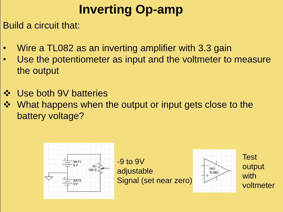
Inverting Op-amp
Build a circuit that:
• Wire a TL082 as an inverting amplifier with 3.3 gain
• Use the potentiometer as input and the voltmeter to measure
the output
Use both 9V batteries
What happens when the output or input gets close to the
battery voltage?
-9 to 9V
adjustable
Signal (set near zero)
Test
output
with
voltmeter

Analog circuits – filtering and
detection
IR
detect
DC
block
Amplify Filter
Peak
detect
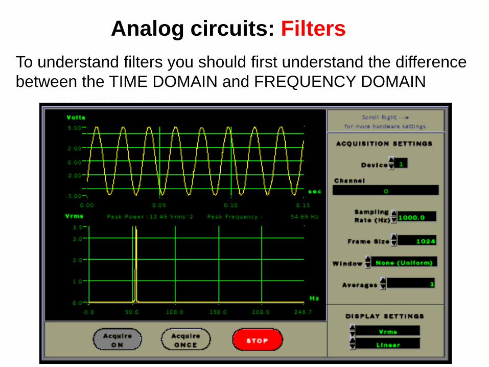
Analog circuits: Filters
To understand filters you should first understand the difference
between the TIME DOMAIN and FREQUENCY DOMAIN
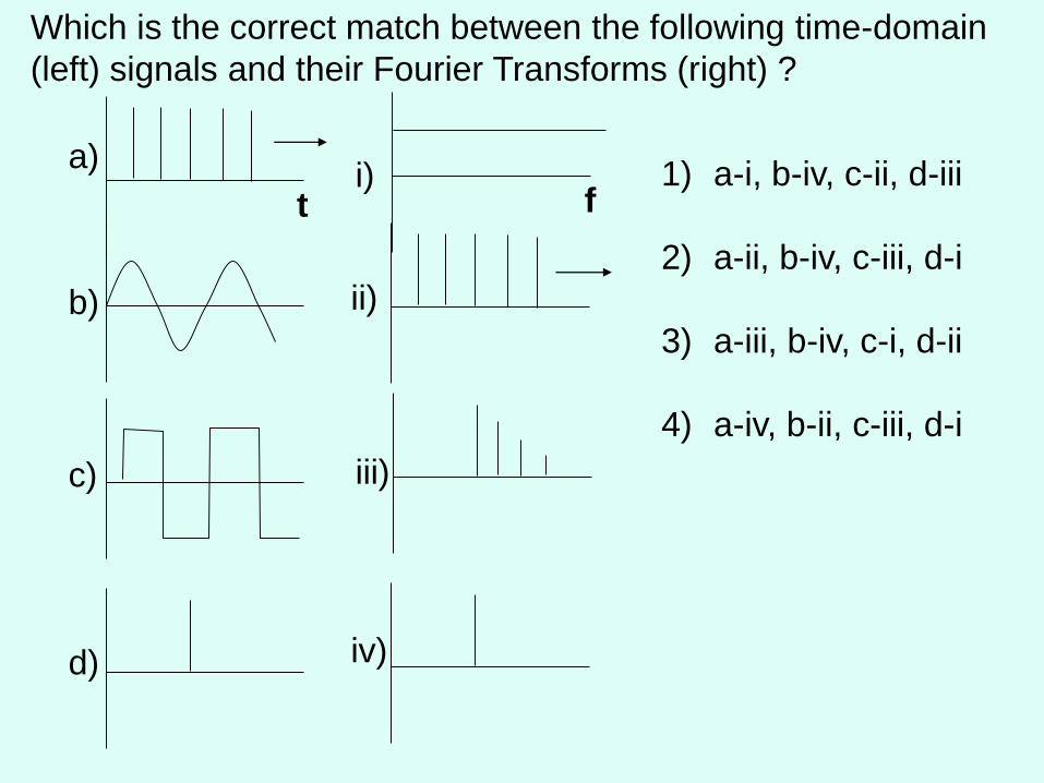
Which is the correct match between the following time-domain
(left) signals and their Fourier Transforms (right) ?
a)
b)
c)
d)
i)
ii)
iii)
iv)
1) a-i, b-iv, c-ii, d-iii
2) a-ii, b-iv, c-iii, d-i
3) a-iii, b-iv, c-i, d-ii
4) a-iv, b-ii, c-iii, d-i
t f

Analog circuits: Filters
Demo: Frequency generator and Spectrum analyzer
Frequency
Generator
Spectrum
Analyzer
ground
signal
Frequency
Generator
Spectrum
Analyzer
ground
Z1
Z2
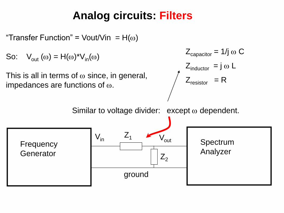
Analog circuits: Filters
Vin Vout
“Transfer Function” = Vout/Vin = H(w)
So: Vout (w) = H(w)*Vin(w)
This is all in terms of w since, in general,
impedances are functions of w.
Similar to voltage divider: except w dependent.
Zcapacitor = 1/j w C
Zinductor = j w L
Zresistor = R
Frequency
Generator
Spectrum
Analyzer
ground
Z1
Z2
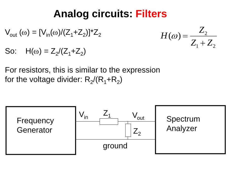
Analog circuits: Filters
Vin Vout
Vout (w) = [Vin(w)/(Z1+Z2)]*Z2
So: H(w) = Z2/(Z1+Z2)
For resistors, this is similar to the expression
for the voltage divider: R2/(R1+R2)
21
2)(ZZ
ZH
w
Frequency
Generator
Spectrum
Analyzer
Z1
Z2
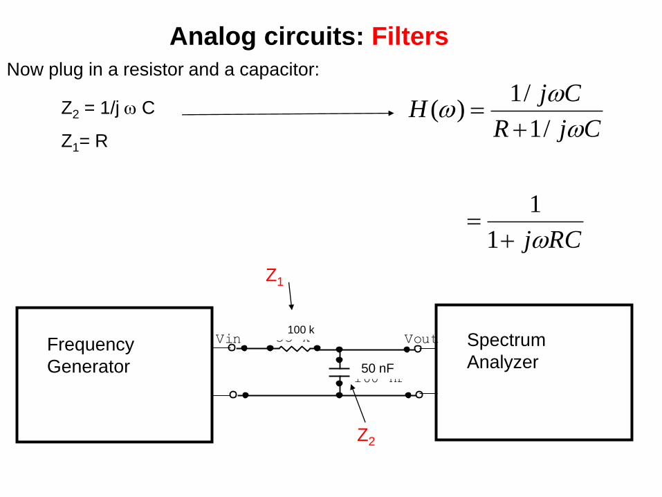
Analog circuits: Filters
Now plug in a resistor and a capacitor:
VoutVinR1
33 k
C1100 nF
100 k
50 nF
Z2 = 1/j w C
Z1= R
RCj
CjR
CjH
w
w
ww
1
1
/1
/1)(
Frequency
Generator
Spectrum
Analyzer
Z1
Z2
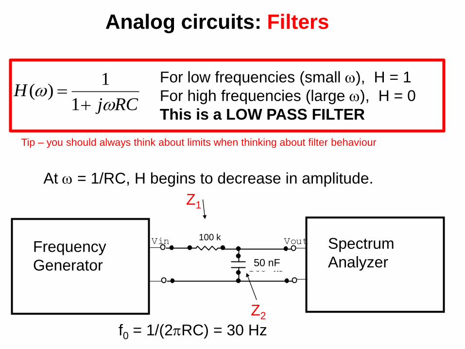
Analog circuits: Filters
For low frequencies (small w), H = 1
For high frequencies (large w), H = 0
This is a LOW PASS FILTERRCj
Hw
w
1
1)(
VoutVinR1
33 k
C1100 nF
f0 = 1/(2pRC) = 30 Hz
100 k
50 nF
At w = 1/RC, H begins to decrease in amplitude.
Tip – you should always think about limits when thinking about filter behaviour
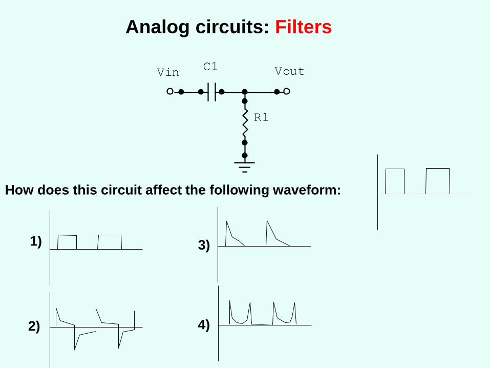
Analog circuits: Filters
VoutVin
R1
C1
How does this circuit affect the following waveform:
1)
2)
3)
4)
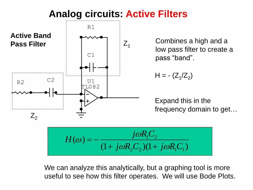
Analog circuits: Active Filters
C2R2
R1
C1
U1TL082
Z2
Z1
)1)(1()(
1122
21
CRjCRj
CRjH
ww
ww
Active Band
Pass Filter Combines a high and a
low pass filter to create a
pass “band”.
H = - (Z1/Z2)
Expand this in the
frequency domain to get…
We can analyze this analytically, but a graphing tool is more
useful to see how this filter operates. We will use Bode Plots.

Analog circuits: Transfer Functions
Bode plots: a graphical representation of frequency response on
logarithmic axes.
20log10(H)
(20 is used instead of 10 so the result will
represent power ~ V2)
-3 dB = ½ as much power as 0 dB
Vout is 1/√2 of Vin at -3dB
Vertical axis:
log10(f)Log of frequency is used to ensure linear
plots from 1/f or 1/fn functions
Horizontal axis:
Pole: 1/(1+j w / w 0)
Zero: (1+j w / w 0)
-20 db/decade in amplitude after w0, -90 phase
+20 db/decade in amplitude after w0, +90 phase

Analog circuits: Transfer Functions
Bode plots: a graphical representation of frequency response on
logarithmic axes.
Pole: 1/(1+j w / w 0)
Zero: (1+j w / w 0)
-20 db/decade in amplitude after w 0, -90 phase
+20 db/decade in amplitude after w0, +90 phase
)1)(1()(
1122
21
CRjCRj
CRjH
ww
ww
Zero at w =0
Pole at w =1/(R2C2) Pole at w =1/(R1C1)

Analog circuits: Simple Pole
RCjH
ww
1
1)(
-3dB, 1/RC - 45 deg, 1/RC
Bode Plot:
-20db/decade
-90 deg
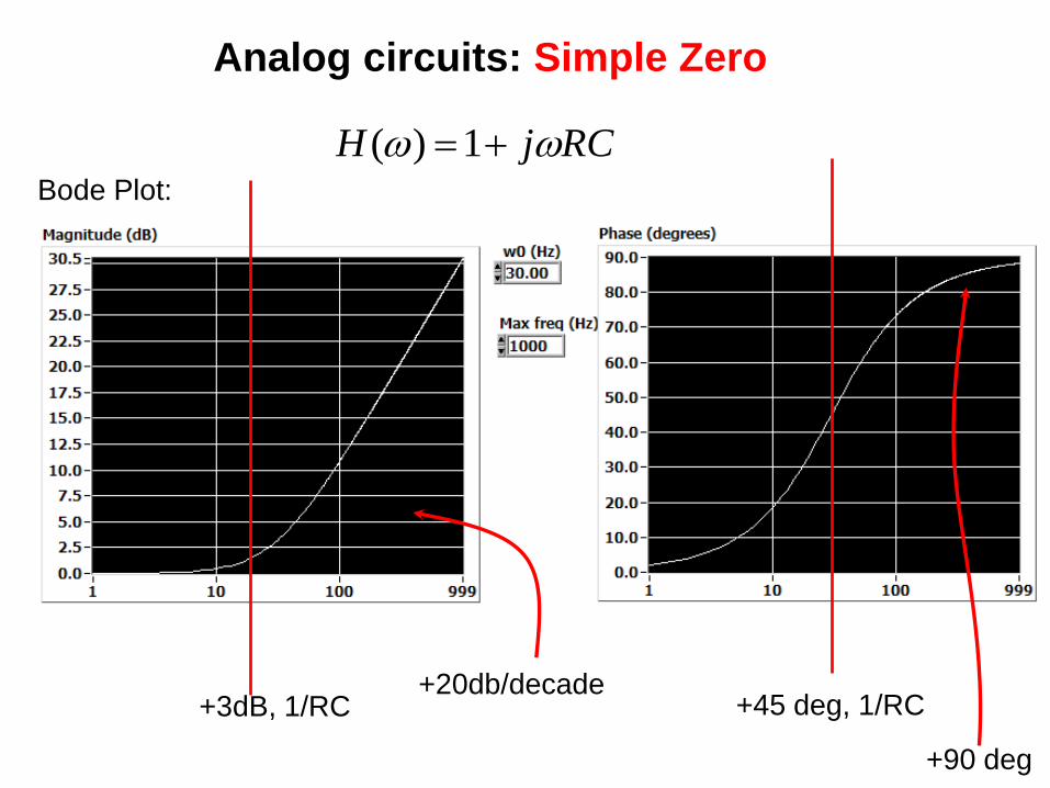
Analog circuits: Simple Zero
RCjH ww 1)(
+3dB, 1/RC +45 deg, 1/RC
Bode Plot:
+20db/decade
+90 deg
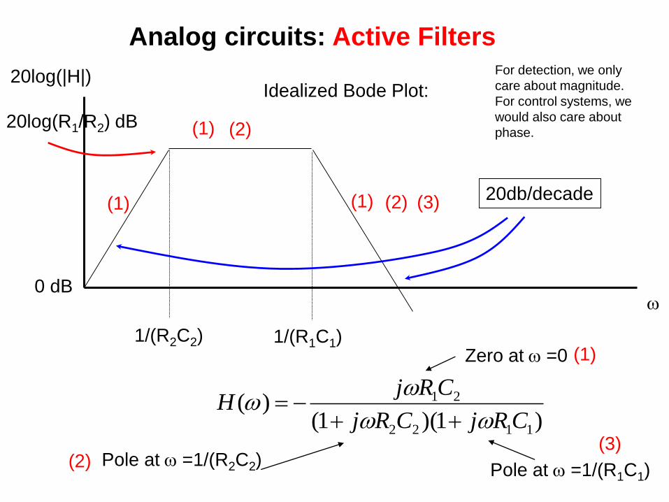
Analog circuits: Active Filters
)1)(1()(
1122
21
CRjCRj
CRjH
ww
ww
Idealized Bode Plot:
Zero at w =0
Pole at w =1/(R2C2) Pole at w =1/(R1C1)
w
20log(|H|)
0 dB
20log(R1/R2) dB
1/(R2C2) 1/(R1C1)(1)
(2)(3)
(1)
(1)
(1)
(2)
(2) (3) 20db/decade
For detection, we only
care about magnitude.
For control systems, we
would also care about
phase.
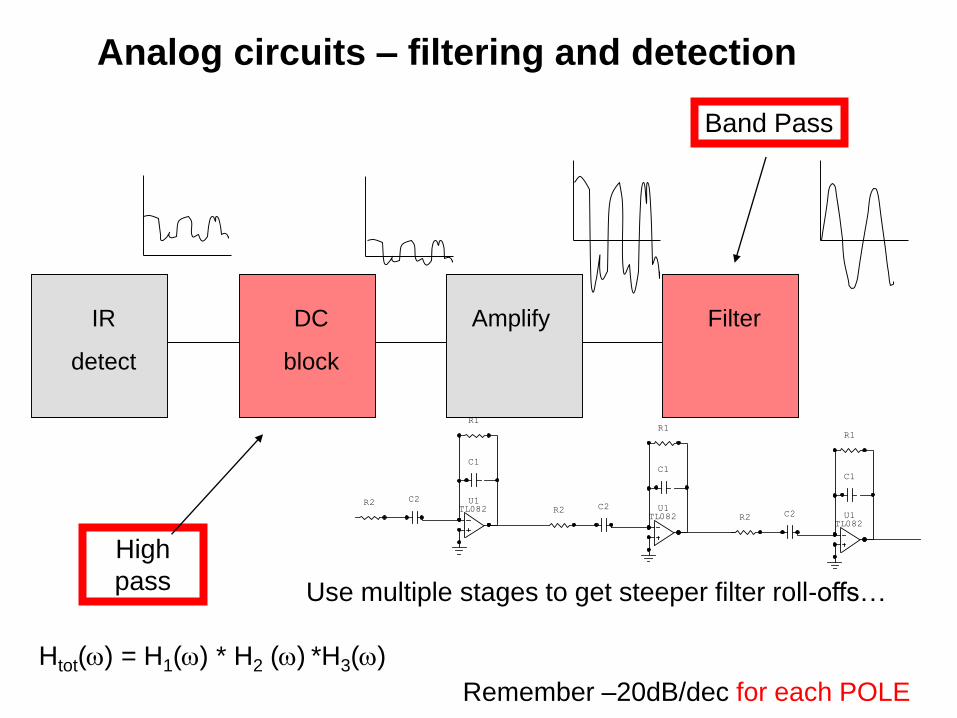
Analog circuits – filtering and detection
IR
detect
DC
block
Amplify Filter
High
pass
Band Pass
C2R2
R1
C1
U1TL082 C2R2
R1
C1
U1TL082 C2R2
R1
C1
U1TL082
Use multiple stages to get steeper filter roll-offs…
Htot(w) = H1(w) * H2 (w) *H3(w)
Remember –20dB/dec for each POLE
49
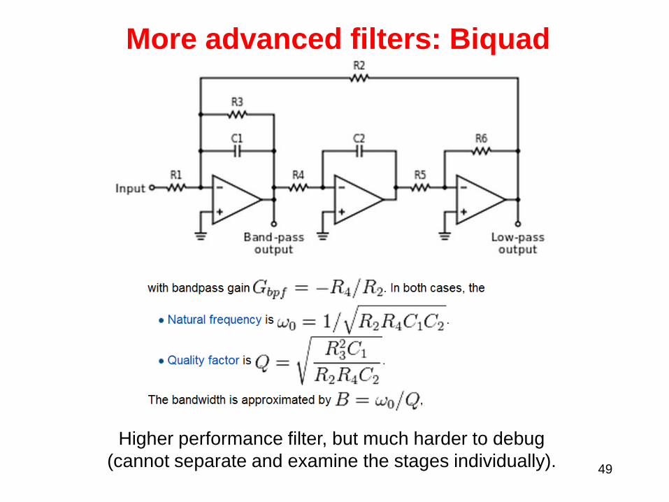
More advanced filters: Biquad
Higher performance filter, but much harder to debug
(cannot separate and examine the stages individually).
Analog circuits – filtering and
detection
IR
detect
DC
block
Amplify Filter
Peak
detect
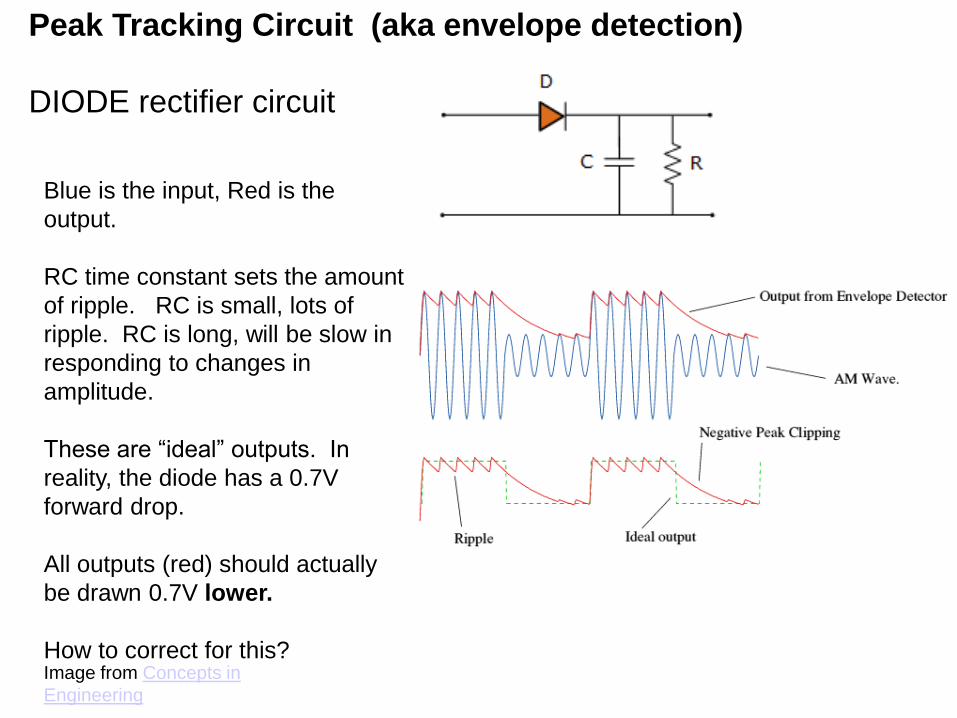
Peak Tracking Circuit (aka envelope detection)
DIODE rectifier circuit
Image from Concepts in
Engineering
Blue is the input, Red is the
output.
RC time constant sets the amount
of ripple. RC is small, lots of
ripple. RC is long, will be slow in
responding to changes in
amplitude.
These are “ideal” outputs. In
reality, the diode has a 0.7V
forward drop.
All outputs (red) should actually
be drawn 0.7V lower.
How to correct for this?
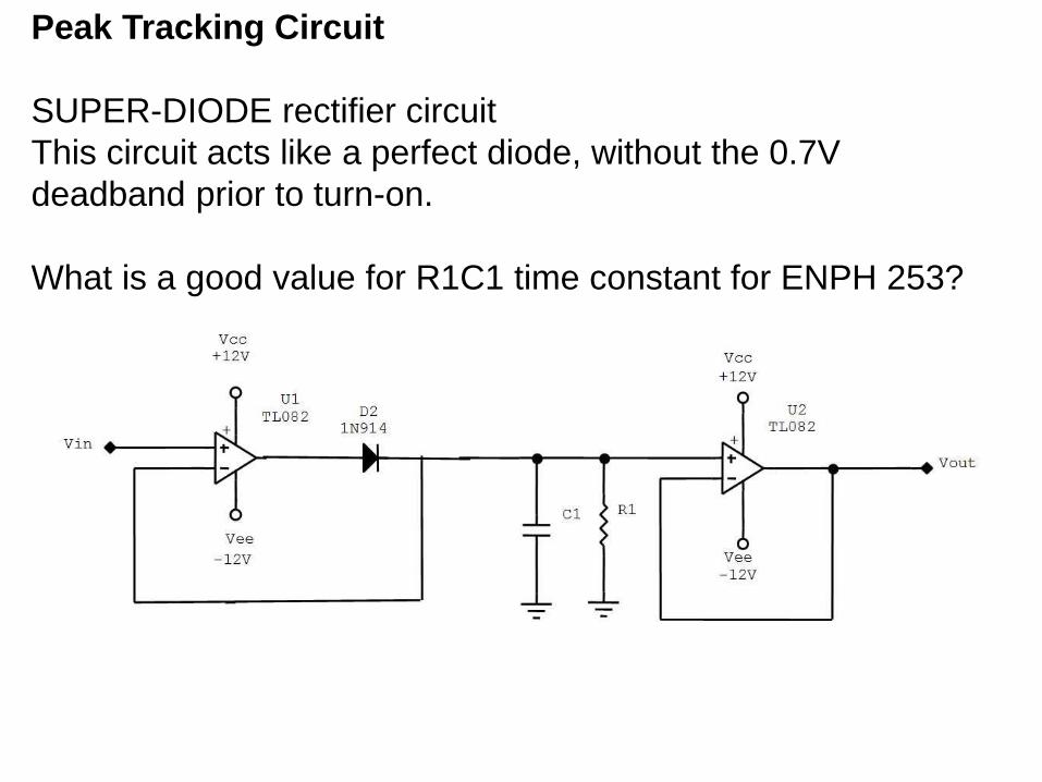
Peak Tracking Circuit
SUPER-DIODE rectifier circuit
This circuit acts like a perfect diode, without the 0.7V
deadband prior to turn-on.
What is a good value for R1C1 time constant for ENPH 253?


![JOURNAL OF IEEE TRANSACTIONS ON CIRCUITS AND SYSTEMS … Zhang's Homepage_files/T… · [1]–[5], which aims to detect object instances of the predefined categories. Accurate object](https://img.pdfslide.net/doc/110x75/5ec881a437185c26cf048ba0/journal-of-ieee-transactions-on-circuits-and-systems-zhangs-homepagefilest.jpg)